EP3316448B1 - Appareil de réception de puissance sans fil - Google Patents
Appareil de réception de puissance sans fil Download PDFInfo
- Publication number
- EP3316448B1 EP3316448B1 EP16814764.3A EP16814764A EP3316448B1 EP 3316448 B1 EP3316448 B1 EP 3316448B1 EP 16814764 A EP16814764 A EP 16814764A EP 3316448 B1 EP3316448 B1 EP 3316448B1
- Authority
- EP
- European Patent Office
- Prior art keywords
- unit
- wireless power
- pattern
- soft magnetic
- transmission side
- Prior art date
- Legal status (The legal status is an assumption and is not a legal conclusion. Google has not performed a legal analysis and makes no representation as to the accuracy of the status listed.)
- Active
Links
Images






Classifications
-
- H—ELECTRICITY
- H01—ELECTRIC ELEMENTS
- H01F—MAGNETS; INDUCTANCES; TRANSFORMERS; SELECTION OF MATERIALS FOR THEIR MAGNETIC PROPERTIES
- H01F27/00—Details of transformers or inductances, in general
- H01F27/24—Magnetic cores
- H01F27/25—Magnetic cores made from strips or ribbons
-
- H—ELECTRICITY
- H02—GENERATION; CONVERSION OR DISTRIBUTION OF ELECTRIC POWER
- H02J—ELECTRIC POWER NETWORKS; CIRCUIT ARRANGEMENTS OR SYSTEMS FOR SUPPLYING OR DISTRIBUTING ELECTRIC POWER; SYSTEMS FOR STORING ELECTRIC ENERGY
- H02J50/00—Circuit arrangements or systems for wireless supply or distribution of electric power
- H02J50/10—Circuit arrangements or systems for wireless supply or distribution of electric power using inductive coupling
- H02J50/12—Circuit arrangements or systems for wireless supply or distribution of electric power using inductive coupling of the resonant type
-
- H—ELECTRICITY
- H01—ELECTRIC ELEMENTS
- H01F—MAGNETS; INDUCTANCES; TRANSFORMERS; SELECTION OF MATERIALS FOR THEIR MAGNETIC PROPERTIES
- H01F1/00—Magnets or magnetic bodies characterised by the magnetic materials therefor; Selection of materials for their magnetic properties
- H01F1/01—Magnets or magnetic bodies characterised by the magnetic materials therefor; Selection of materials for their magnetic properties of inorganic materials
- H01F1/03—Magnets or magnetic bodies characterised by the magnetic materials therefor; Selection of materials for their magnetic properties of inorganic materials characterised by their coercivity
- H01F1/12—Magnets or magnetic bodies characterised by the magnetic materials therefor; Selection of materials for their magnetic properties of inorganic materials characterised by their coercivity of soft-magnetic materials
-
- H—ELECTRICITY
- H01—ELECTRIC ELEMENTS
- H01F—MAGNETS; INDUCTANCES; TRANSFORMERS; SELECTION OF MATERIALS FOR THEIR MAGNETIC PROPERTIES
- H01F1/00—Magnets or magnetic bodies characterised by the magnetic materials therefor; Selection of materials for their magnetic properties
- H01F1/01—Magnets or magnetic bodies characterised by the magnetic materials therefor; Selection of materials for their magnetic properties of inorganic materials
- H01F1/03—Magnets or magnetic bodies characterised by the magnetic materials therefor; Selection of materials for their magnetic properties of inorganic materials characterised by their coercivity
- H01F1/12—Magnets or magnetic bodies characterised by the magnetic materials therefor; Selection of materials for their magnetic properties of inorganic materials characterised by their coercivity of soft-magnetic materials
- H01F1/14—Magnets or magnetic bodies characterised by the magnetic materials therefor; Selection of materials for their magnetic properties of inorganic materials characterised by their coercivity of soft-magnetic materials metals or alloys
-
- H—ELECTRICITY
- H01—ELECTRIC ELEMENTS
- H01F—MAGNETS; INDUCTANCES; TRANSFORMERS; SELECTION OF MATERIALS FOR THEIR MAGNETIC PROPERTIES
- H01F1/00—Magnets or magnetic bodies characterised by the magnetic materials therefor; Selection of materials for their magnetic properties
- H01F1/01—Magnets or magnetic bodies characterised by the magnetic materials therefor; Selection of materials for their magnetic properties of inorganic materials
- H01F1/03—Magnets or magnetic bodies characterised by the magnetic materials therefor; Selection of materials for their magnetic properties of inorganic materials characterised by their coercivity
- H01F1/12—Magnets or magnetic bodies characterised by the magnetic materials therefor; Selection of materials for their magnetic properties of inorganic materials characterised by their coercivity of soft-magnetic materials
- H01F1/14—Magnets or magnetic bodies characterised by the magnetic materials therefor; Selection of materials for their magnetic properties of inorganic materials characterised by their coercivity of soft-magnetic materials metals or alloys
- H01F1/16—Magnets or magnetic bodies characterised by the magnetic materials therefor; Selection of materials for their magnetic properties of inorganic materials characterised by their coercivity of soft-magnetic materials metals or alloys in the form of sheets
-
- H—ELECTRICITY
- H01—ELECTRIC ELEMENTS
- H01F—MAGNETS; INDUCTANCES; TRANSFORMERS; SELECTION OF MATERIALS FOR THEIR MAGNETIC PROPERTIES
- H01F27/00—Details of transformers or inductances, in general
- H01F27/34—Special means for preventing or reducing unwanted electric or magnetic effects, e.g. no-load losses, reactive currents, harmonics, oscillations, leakage fields
- H01F27/36—Electric or magnetic shields or screens
-
- H—ELECTRICITY
- H01—ELECTRIC ELEMENTS
- H01F—MAGNETS; INDUCTANCES; TRANSFORMERS; SELECTION OF MATERIALS FOR THEIR MAGNETIC PROPERTIES
- H01F27/00—Details of transformers or inductances, in general
- H01F27/34—Special means for preventing or reducing unwanted electric or magnetic effects, e.g. no-load losses, reactive currents, harmonics, oscillations, leakage fields
- H01F27/36—Electric or magnetic shields or screens
- H01F27/366—Electric or magnetic shields or screens made of ferromagnetic material
-
- H—ELECTRICITY
- H01—ELECTRIC ELEMENTS
- H01F—MAGNETS; INDUCTANCES; TRANSFORMERS; SELECTION OF MATERIALS FOR THEIR MAGNETIC PROPERTIES
- H01F38/00—Adaptations of transformers or inductances for specific applications or functions
- H01F38/14—Inductive couplings
-
- H—ELECTRICITY
- H02—GENERATION; CONVERSION OR DISTRIBUTION OF ELECTRIC POWER
- H02J—ELECTRIC POWER NETWORKS; CIRCUIT ARRANGEMENTS OR SYSTEMS FOR SUPPLYING OR DISTRIBUTING ELECTRIC POWER; SYSTEMS FOR STORING ELECTRIC ENERGY
- H02J50/00—Circuit arrangements or systems for wireless supply or distribution of electric power
- H02J50/70—Circuit arrangements or systems for wireless supply or distribution of electric power involving the reduction of electric, magnetic or electromagnetic leakage fields
-
- H02J7/025—
-
- H—ELECTRICITY
- H04—ELECTRIC COMMUNICATION TECHNIQUE
- H04B—TRANSMISSION
- H04B5/00—Near-field transmission systems, e.g. inductive or capacitive transmission systems
- H04B5/70—Near-field transmission systems, e.g. inductive or capacitive transmission systems specially adapted for specific purposes
- H04B5/79—Near-field transmission systems, e.g. inductive or capacitive transmission systems specially adapted for specific purposes for data transfer in combination with power transfer
Definitions
- the present invention relates to a wireless power receiving apparatus
- Wireless power transmitting/receiving technology is a technology which wirelessly supplies power to electronic devices.
- a soft magnetic material may be disposed around a transmitting antenna and a receiving antenna so that electromagnetic energy radiated by the transmitting antenna can be focused in a direction of the receiving antenna.
- a soft magnetic layer is a sheet containing a ferrite material
- magnetic permeability is good, however, there is a limitation related to a thickness of the soft magnetic layer due to the limitation related to the high-temperature firing and magnetic flux density.
- a soft magnetic layer is a sheet which has a composite form containing a metal powder and a polymer resin, there is a problem in terms of lower magnetic permeability.
- a soft magnetic layer is a metal ribbon
- US 2014/239892 A1 discloses providing incisions in thin magnetic plates.
- Embodiments of the present invention provide a wireless power receiving apparatus and a wireless power transfer system including the wireless power receiving apparatus.
- the present invention relates to a wireless power receiving apparatus for charging power wirelessly as set out in claim 1.
- Embodiments of the invention are defined in dependent claims 2-6.
- a metal ribbon with high actual permeability within a frequency range which is used in wireless charging. Accordingly, it may be possible to obtain a wireless power transfer system not only having a slim shape but also having high efficiency in power transferring.
- Embodiments selectively use a variety type of frequency bands ranging from low frequency (50 kHz) to high frequency (15MHz) for wireless power transfer, and require support of a communication system capable of exchanging data and controlling signals for controlling system.
- Embodiments may be applied to various industrial fields such as a mobile terminal industry, a smart watch industry, a computer and laptop industry, a household appliances industry, an electric vehicle industry, a medical device industry and a robot industry, which use or require a battery.
- Embodiments may take into consideration a system capable of transferring power to at least one device using one or a plurality of transfer coils provided in the device.
- wireless power transfer technology is applied to household electrical appliances such as vacuum cleaners, fans, etc.
- household electrical appliances such as vacuum cleaners, fans, etc.
- complex wires can be eliminated in the home, which can reduce the amount of wiring in buildings and increase efficiency of the utility of space.
- it takes a lot of time to charge an electric car with a current household power source; however, when transferring high power through wireless power transfer technology, it is possible to reduce the charge time.
- a wireless charging facility on a floor of a parking lot, it is possible to eliminate inconvenience related to preparing a power cable near an electric car.
- one of the principles of wireless power transfer is related to a magnetic induction method.
- the magnetic induction method is a non-contact energy transfer technology in which an electromotive force is generated in a load inductor Ll via magnetic flux generated when a source inductor Ls and the load inductor Ll are brought to be close to each other and current is supplied to one of the source inductors Ls.
- Fig. 1 illustrates a diagram of a magnetic induction method equivalent circuit.
- the transmitting unit in a magnetic induction method equivalent circuit may be embodied by a source voltage Vs depending on an apparatus supplying power source, a source resistance Rs, a source capacitor Cs to match impedance and a source coil Ls to magnetically couple with a receiving unit, and the receiving unit may be shown by a load resistance R1 which is an equivalent resistance of the receiving unit, a load capacitor Cl to match impedance and a load coil Ll to magnetically couple with the transmitting unit, wherein a degree of magnetic coupling of the source coil Ls and the load coil Ll may be shown by mutual inductance Msl.
- equation 1 when a ratio of the inductance of the transmitting coil Ls to the source resistance Rs and a ratio of the load coil Ll to the load resistance Rl are the same, maximum power transfer becomes possible. Because there is no capacitors to compensate for reactance in a system in which only inductance is present, the self reflection value S11 of the input/output port at a point at which the maximum power delivery is created cannot be 0, and efficiency of power delivery may vary greatly based on the value of the mutual inductance Msl. Accordingly, the source capacitor Cs may be added to the transmitting unit as a compensation capacitor, and the load capacitor Cl may be added to the receiving unit.
- the compensation capacitors Cs and Cl may be connected in series or in parallel to, for example, the receiving coil Ls and the load coil Ll respectively.
- passive elements such as additional capacitors and inductors as well as the compensation capacitor may be added to each of the transmitting unit and the receiving unit.
- Fig. 2 is a block diagram showing a transmitting unit as one of the subsystems which constitute a wireless power transfer system.
- the wireless power transfer system may include a transmitting unit 1000 and a receiving unit 2000 to which power is wirelessly transferred from the transmitting unit 1000, wherein the transmitting unit 1000 may include an AC/DC conversion unit 1100 at the transmission side, a DC/AC conversion unit 1200 at the transmission side, an impedance matching unit 1300 at the transmission side, a transmitting coil unit 1400, and a communication and control unit 1500 at the transmission side.
- the transmitting unit 1000 may be alternatively used with a wireless power transmitting apparatus.
- the AC/DC conversion unit 1100 at the transmission side is a power conversion unit that converts an AC signal provided from the outside under the control of the communication and control unit 1500 at the transmission side into a DC signal
- the AC/DC conversion unit 1100 at the transmission side may include a rectifier 1110 and a DC/DC conversion unit 1120 at the transmission side as a subsystem.
- the rectifier 1110 is a system that converts an AC signal that has been provided into a DC signal and, as in the embodied examples, the rectifier 1110 may be a diode rectifier which has relatively high efficiency when operated at a high frequency, a synchronous rectifier which is capable of being a one-chip type or a hybrid rectifier which is able to save cost and space and have a high degree of freedom in Dead time.
- the AC/AC conversion unit 1120 at the transmission side regulates a level of an AC signal provided from the rectifier 1110 under the control of the communication and control unit 1500 at the transmission side, and as in the embodied examples, the AC/AC conversion unit 1120 may be a Buck converter which lowers a level of an input signal, a Boost converter which raises a level of an input signal, a Buck Boost converter which is able to lower or raise a level of an input signal, or a Cuk converter.
- the AC/AC conversion unit 1120 at the transmission side may include switch elements which serve as a power conversion control function, inductors and capacitors which serve a power conversion parameter role or serve as an output voltage smoothing function, trances which serve to regulate voltage gains or serve as an electrical separation function (an insulation function), etc., and the AC/AC conversion unit 1120 at the transmission side may serve to eliminate ripple components included in the input AC signal or to pulsate components (alternative components included in a AC signal). Furthermore, a difference between a command value of the output signal of the AC/AC conversion unit 1120 at the transmission side and an actual output value may be regulated via a feedback method, which can be performed through the communication and control unit 1500 at the transmission side.
- the DC/AC conversion unit 1200 at the transmission side is a system that converts an DC signal output from the AC/DC conversion unit 1100 at the transmission side under the control of the communication and control unit 1500 at the transmission side into a AC signal, and regulates a frequency of the converted AC signal, and as in the embodied examples, there is a Half bridge inverter or a Full bridge inverter.
- the DC/AC conversion unit 1200 at the transmission side may include oscillators which generate a frequency of the output signal and power amplifiers which amplify the output signal.
- the impedance matching unit 1300 at the transmission side improves a flow of a signal by minimizing a reflection wave at points having different impedance. Since the two coils of the transmitting unit 1000 and the receiving unit 2000 are spatially separated and thus leakage of the magnetic field is large, it is possible to improve the efficiency of the power delivery by correcting differences of the impedance between two connecting ends of the transmitting unit 1000 and the receiving unit 2000.
- the impedance matching unit 1300 at the transmission side may be composed of an inductor, a capacitor and a resistance element, and may regulate an impedance value to match the impedance by varying inductance of the inductor, capacitance of the capacitor and a value of resistance of the resistance element under the control of the communication and control unit 1500.
- the impedance matching unit 1300 at the transmission side may have a serial resonance structure or a parallel resonance structure, and it is possible to minimize energy loss by increasing an inductance coupling coefficient between the transmitting unit 1000 and the receiving unit 2000.
- the coil 1400 at the transmitting side may be embodied by a number of coils or a single coil.
- the coils may be arranged to be apart from each other, or arranged to be overlapped with each other.
- the overlapped area can be determined by taking into consideration of a deviation of a magnetic flux density.
- the coil 1400 may be manufactured by taking into consideration of internal resistance and radiation resistance. At that time, when the resistance component is small, the Quality factor can be increased and the transfer efficiency can be improved.
- the communication and control unit 1500 is a subsystem and may include a control unit 1510 at the transmission side and a communication unit 1520 at the transmission side.
- the control unit 1510 at the transmission side may serve to regulate the output voltage of the AC/DC conversion unit 1100 at the transmission side by taking into consideration of a required amount of power, a current amount of charge and the wireless power method of the receiving unit 2000.
- it is possible to control overall operation of the receiving unit 2000 by using an algorithm, a program, or an application required to control what is read from a storage unit (not shown) of the receiving unit 2000.
- control unit 1510 at the transmission side may be referred to as a microprocessor, a Micro Controller Unit or a Micom.
- the communication unit 1520 at the transmission side may communicate with a communication unit 2620 at a reception side, and a bluetooth method may be used as one example of a communication method.
- the communication unit 1520 at the transmission side and the communication unit 2620 at the reception side can transmit and receive charge status information and charge control commands and the like between each other.
- charge status information the number of the receiving units 2000, a remaining battery level, the number of charging, an amount of usage, a capacity of a battery, a ratio of a battery and a transfer amount of power of the transmitting unit 1000 may be included.
- the communication unit 1520 at the transmission side may transmit a charge function control signal which controls a charge function of the receiving unit 2000, and the charge function control signal may be a control signal that controls the receiving unit 2000 so as to enable or disable the charge function.
- the transmitting unit 1000 may composed of hardware which is different from that of the communication unit 1520 at the transmission side, therefore the transmitting unit 1000 may communicate with an out-band method.
- the transmitting unit 1000 and the communication unit 1520 at the transmission side may be embodied as one hardware unit, and therefore, the transmitting unit 1000 may communicate with an in-band method.
- the communication unit 1520 at the transmission side and the control unit 1510 at the transmitting side may be composed separately, and also in the receiving unit 2000, the communication unit 2620 at the reception side may be included in a control unit of the receiving apparatus or composed separately from the control unit thereof.
- Fig. 3 is a block diagram showing a receiving unit as one of the subsystems which constitutes a wireless power transfer system.
- the wireless power transfer system may include the transmitting unit 1000 and the receiving unit 2000 to which power is wirelessly transferred from the transmitting unit 1000, wherein the receiving unit 2000 may include a coil unit 2100 at the reception side, a matching unit 2200 at the reception side, an AC/DC conversion unit 2300 at the reception side, a DC/DC conversion unit 2400 at the reception unit, a load unit 2500 at the reception side and a communication and control unit 2600 at the reception side.
- the receiving unit 2000 may be alternatively used with a wireless power receiving apparatus.
- the coil unit 2100 at the reception side may receive power through a magnetic induction method, and a single induction coil or a plurality of induction coils may be provided.
- the coil unit 2100 at the reception side may be provided with an antenna for near field communication.
- the coil unit 2100 at the reception side may be the same as the coil unit 1400 at the transmission side.
- the size of the receiving antenna may depend on electrical characteristics of the receiving unit 2000.
- the matching unit 2200 at the reception side performs impedance matching between the transmitting unit 1000 and the receiving unit 2000.
- the AC/DC conversion unit 2300 at the reception side generates a DC signal by rectifying the AC signal, which is output from the coil unit 2100 at the reception side.
- the DC/DC conversion unit 2400 at the reception side can regulate a level of the DC signal, which is output from the AC/DC conversion unit 2300 at the reception unit, to be adapted to a capacity of the load unit 2500.
- the load unit 2500 may include a battery, a display, a sound output circuit, a main processor, and various sensors.
- the communication and control unit 2600 at the reception unit may be activated by wake-up power from the communication and control unit 1500 at the transmission side, perform communication with the communication and control unit 1500 at the transmission side, and control an operation of the subsystem of the receiving unit 2000.
- the receiving unit 2000 may be embodied in a single receiving unit or a plurality of receiving units, and energy can be wirelessly delivered from the transmitting unit 1000 simultaneously.
- a plurality of target receiving units 2000 may be supplied with power from one transmitting unit 1000 as a result of having a plurality of coil units at the reception side, which are independent of each other.
- the matching unit 1300 at the transmission side of the transmitting unit 1000 may adaptively perform impedance matching among the plurality of the receiving units 2000.
- the system of the receiving units 2000 may be of the same type or a different type.
- an AC signal of 60 Hz having 110V to 220V may be applied to the AC/DC conversion unit 1100 at the transmission side, and the AC/DC conversion unit 1100 may convert the AC signal into a DC signal having 10V to 20V and output the signal, and the DC signal may be applied to the DC/AC conversion unit 1200 at the transmission side, and the DC/AC conversion unit 1200 may output a AC signal of 125 KHZ.
- the AC signal of 125 KHz may be input to the AC/DC conversion unit 2300 at the reception side of the receiving unit 2000, and the AC/DC conversion unit 2300 may convert the AC signal into a DC signal having 10V to 20V, and the DC/DC conversion unit 2400 at the reception side may output a DC signal which is appropriate for the load unit 2500, for example, a DC signal having 5V, and deliver it to the load unit 2500.
- Fig. 4 is a drawing showing a part of a wireless power transmitting apparatus according to one embodiment of the present invention
- Fig. 5 is a drawing showing a part of a wireless power receiving apparatus according to one embodiment of the present invention.
- the wireless power transmitting apparatus may be a part of a component of the transmitting unit 1000
- the wireless power transmitting apparatus may be a part of a component of the receiving unit 2000.
- a wireless power transmitting apparatus 100 includes a transmitting circuit (not shown), a soft magnetic core 110, a transmitting coil 120 and a permanent magnet 130.
- the soft magnetic core 110 may be made of a soft magnetic material having a thickness of several mm.
- the permanent magnet 130 may be surrounded by the transmitting coil 120.
- the permanent magnet 130 is not an essential component, and may be omitted according to specifications.
- the wireless power receiving apparatus 200 includes a receiving circuit (not shown), a soft magnetic layer 210, and a receiving coil 220.
- the soft magnetic layer 210 may be laminated on a substrate (not shown).
- the substrate may be made of multiple layers of fixed sheets, may be bonded to the soft magnetic layer 210, and then make the soft magnetic layer 210 to be fixed.
- the soft magnetic layer 210 focuses electromagnetic energy which is radiated from the transmitting coil 120 of the wireless power transmitting apparatus 100.
- the receiving coil 220 is laminated on the soft magnetic layer 210.
- the receiving coil 220 may be wound in a parallel direction with the soft magnetic layer 210 on the soft magnetic layer 210.
- the receiving coil may be in a form of a spiral coil having an outer diameter of 50 mm or less and an inner diameter of 20 mm or more.
- the receiving circuit converts the received electromagnetic energy into electric energy via the receiving coil 220 and charges a battery (not shown) with the converted electric energy.
- a heat-radiating layer may be further included between the soft magnetic layer 210 and the receiving coil 220.
- a substrate, the soft magnetic layer 210 and the receiving coil 220 may be referred to as a receiving antenna.
- a NFC coil 230 may be further laminated on the soft magnetic layer 210.
- the NFC coil 230 may be configured to surround an outer circumference of the receiving coil 220.
- both of the receiving coil 220 and the NFC coil 230 may be electrically connected via terminals 240.
- the soft magnetic layer 210 is a sheet containing a ferrite, there is good magnetic permeability, however, there is a limitation related to a thickness of the soft magnetic layer due to the limitation with respect o high-temperature firing and magnetic flux density.
- the soft magnetic layer 210 is a sheet which has a composite form containing a metal powder and a polymer resin, there is a problem in terms of a lower magnetic permeability due to the polymer resin.
- the soft magnetic layer 210 is a metal ribbon, it is possible to attain high magnetic permeability and magnetic flux density with a thin thickness.
- the metal ribbon has a severe problem in terms of magnetic loss in a frequency area used for wireless charging.
- the soft magnetic layer 210 While a metal ribbon is used as the soft magnetic layer 210, it is intended to reduce eddy current loss caused by cracks being formed on the metal ribbon.
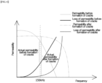
- Fig. 6 is a graph comparing actual permeability per frequency before and after a crack is formed on a metal ribbon.
- a difference between magnetic permeability and a loss of magnetic permeability may mean the actual permeability.
- the actual permeability after cracks are formed in the metal ribbon is significantly higher than the actual permeability before the cracks are formed.
- a metal ribbon means a noncrystalline or a nanocrystalline metal or an alloy made of very thin foil via techniques such as Atomizer.
- a thickness of the metal ribbon may be, for example, 0.01 mm to 0.04 mm.
- the metal ribbon may be a metal ribbon containing Fe.
- the metal ribbon As the soft magnetic layer 210 of the wireless power receiving apparatus 200, it is possible to reduce an eddy current loss and improve the efficiency of transfer by forming cracks on the metal ribbon.
- the effect of improving the transfer efficiency can be decreased, and the performance of the soft magnetic layer becomes ununiform so that a problem arises in that reliable results cannot be obtained.
- forming a uniform pattern of cracks on the metal ribbon is intended to improve the transfer efficiency of the soft magnetic layer, and to make the performance of the soft magnetic layer uniform.
- Fig. 7 to Fig. 9 show top views of a soft magnetic substrate.
- a pattern including at least 3 lines 720 which are radiated from a predetermined point 710 is formed on the soft magnetic layer 210.
- the pattern may be formed as cracks.
- a plurality of patterns 700 may be formed repeatedly, and one pattern 700 may be arranged to be surrounded by a plurality of patterns, for example, by 3 to 8 patterns 700.
- a non-pattern area may be formed between the patterns.
- an average diameter of each pattern 700 may be 50 ⁇ m to 600 ⁇ m, preferably 75 ⁇ m to 500 ⁇ m, and more preferably 100 ⁇ m to 300 ⁇ m.
- the diameter of the pattern 700 is less than 50 ⁇ m, there may be a problem in terms of creating excess metal particles on a surface of the metal ribbon when forming cracks. In the case metal particles are present on the surface of the soft magnetic layer 210, there is a risk of circuit shorting because the metal particles may penetrate into the circuit.
- the diameter of the pattern 700 exceeds 600 ⁇ m, the effect of crack formation, that is, the effect of increasing the actual permeability may be decreased because the distance between the patterns 700 is great.
- Fig. 10 and Fig. 11 show top views of soft magnetic substrates.
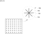
- a pattern 700 including at least 3 lines 720 which are radiated from predetermined points 710, and an edge 730 which is surrounding the lines 720 is formed on the soft magnetic layer 210.
- the pattern may be formed as cracks.
- the edge 730 is not a crack which is completely cut off, but a part of the crack continues and another part of the crack discontinues.
- a plurality of patterns 700 may be formed repeatedly, and one pattern 700 may be arranged to be surrounded by a plurality of patterns, for the present invention, by 3 to 8 patterns 700.
- an average diameter of each pattern 700 may be 50 ⁇ m to 600 ⁇ m, preferably 75 ⁇ m to 500 ⁇ m, and more preferably 100 ⁇ m to 300 ⁇ m.
- the diameter of pattern 700 is less than 50 ⁇ m, there may be a problem in terms of metal particles being created on a surface of the metal ribbon when forming cracks. In the case metal particles are present excessively on the surface of the soft magnetic layer 210, there is a risk of circuit shorting because the metal particles may penetrate into the circuit.
- the diameter of the pattern 700 exceeds 600 ⁇ m, the effect of crack formation, that is, the effect of increasing the actual permeability may be decreased because the distance between the patterns 700 is great.
- the pattern 700 includes the edge 730, the effect of crack formation is further increased, boundaries between the patterns 700 are clearly distinguished, and an aspect of the repetitive pattern becomes clear, so that the uniformity of the quality can be further increased.
- the pattern 700 includes at least 6 lines 720 which are radiated from predetermined points 710, and an edge which surrounds the lines 720. If at least 6 lines 720 which are radiated are formed within the edge 730, the effect of crack formation may be maximized.
- Fig. 12 shows a top view of a soft magnetic substrate.
- a pattern 700 including at least 3 lines 720 which are radiated from predetermined points 710, and an edge 730 which surrounds at least 2 of the lines is formed on the soft magnetic layer 210.
- the pattern may be formed as cracks.
- a plurality of patterns 700 may be formed repeatedly, and one pattern 700 may be arranged to be surrounded by a plurality of patterns, for example, by 3 to 8 patterns 700.
- an average diameter of each pattern 700 may be 50 ⁇ m to 600 ⁇ m, preferably 75 ⁇ m to 500 ⁇ m, and more preferably 100 ⁇ m to 300 ⁇ m.
- the diameter of pattern 700 is less than 50 ⁇ m, there may be a problem in terms of metal particles being created on a surface of the metal ribbon when forming cracks. In the case metal particles are present on the surface of the soft magnetic layer 210, there is a risk of circuit shorting because the metal particles may penetrate into the circuit.
- the diameter of the pattern 700 exceeds 600 ⁇ m, the effect of crack formation, that is, the effect of increasing the actual permeability may be decreased because the distance between the patterns 700 is great.
- the roller may be made of urethane material.
- the roller made of urethane material may form a pattern of cracks more uniformly as compared with a roller made of metal material, and minimize the phenomenon in which metal particles remain on the surface of the metal ribbon.
- a pressing process may be performed under a period of 10 minutes or less at 25 to 200 Pa or 10 to 3000 Pa.
- the metal ribbon on which a repetitive pattern of cracks is formed as a soft magnetic layer of the wireless power receiving apparatus, it is possible to increase magnetic permeability and saturation magnetism, and to reduce the eddy current loss.
- the uniform pattern of cracks on the metal ribbon it is possible to increase the transfer efficiency and to obtain a uniform and predictable performance.
- Table 1 is a table comparing the performance of the transfer efficiency of the wireless power transfer system in the case of using a metal ribbon on which cracks are randomly formed as a soft magnetic layer and a metal ribbon on which a repetitive pattern of cracks is formed as a soft magnetic layer.
- the metal ribbon is a nanocrystalline metal ribbon containing Fe.
- Fig. 13 shows a metal ribbon having random cracks which is used in comparative embodiment 1
- Fig. 14 shows a metal ribbon having repetitive cross-shaped cracks which is used in embodiment 1
- Fig. 15 shows a metal ribbon having repetitive cross-shaped cracks surrounded within an edge which is used in embodiment 2
- the metal ribbon on which a regularly repeated pattern of cracks is formed has higher transfer efficiency than the metal ribbon on which cracks are formed in a random shape.
- a pattern has the highest transfer efficiency when it includes at least 6 lines radiated from predetermined points and an edge surrounding the lines, that is, the pattern has a star-shape which is surrounded by an edge.
- the effects of a repetitive pattern of crack formation may be more advantageous at high power. This is because the intensity of the magnetic field increases with the increase of the amount of current, and the metal ribbon of the receiving unit is affected more by the magnetic field as the intensity of the magnetic field increases.
Landscapes
- Engineering & Computer Science (AREA)
- Power Engineering (AREA)
- Computer Networks & Wireless Communication (AREA)
- Chemical & Material Sciences (AREA)
- Dispersion Chemistry (AREA)
- Physics & Mathematics (AREA)
- Electromagnetism (AREA)
- Signal Processing (AREA)
- Charge And Discharge Circuits For Batteries Or The Like (AREA)
Claims (6)
- Appareil de réception d'énergie sans fil (200) destiné à charger de l'énergie sans fil, comprenant :un substrat ;une couche magnétique douce (210) qui est stratifiée sur le substrat ; etune bobine stratifiée sur un côté de la couche magnétique douce,dans lequel la couche magnétique douce (210) comporte un ruban métallique à base de Fe qui est formé comme des motifs de fissures,dans lequel les motifs de fissures comprennent :un premier motif (700) et une pluralité de deuxièmes motifs (700) disposés pour être adjacents au premier motif (700),dans lequel le nombre de la pluralité de deuxièmes motifs est de 3 à 8,caractérisé en ce quechacun (700) du premier motif et de la pluralité de deuxièmes motifs (700) comporte au moins 6 lignes rayonnées (720) qui sont rayonnées depuis un point prédéterminé (710), etun bord (730) qui entoure les au moins 6 lignes rayonnées (720),dans lequel une partie du bord (730) est découpée, etdans lequel le bord (730) du premier motif (700) et le bord (730) de chacun de la pluralité de deuxièmes motifs (700) sont espacés l'un de l'autre.
- Appareil de réception d'énergie sans fil de la revendication 1, dans lequel le bord (730) du premier motif (700) est formé dans une région qui est plus proche de chaque ligne rayonnée (720) du premier motif (700) que du deuxième motif (700).
- Appareil de réception d'énergie sans fil de la revendication 2, dans lequel une zone sans motif est formée entre le bord du premier motif (700) et le bord (730) de chacun de la pluralité de deuxièmes motifs (700).
- Appareil de réception d'énergie sans fil de la revendication 1, dans lequel un diamètre moyen du premier motif (700) est de 50 pm à 600 pm.
- Appareil de réception d'énergie sans fil de la revendication 1, dans lequel une épaisseur du substrat magnétique doux est de 0,01 mm à 0,04 mm.
- Appareil de réception d'énergie sans fil de la revendication 2, dans lequel un diamètre moyen du premier motif (700) est de 50 µm à 600 µm.
Applications Claiming Priority (2)
| Application Number | Priority Date | Filing Date | Title |
|---|---|---|---|
| KR1020150090740A KR101950369B1 (ko) | 2015-06-25 | 2015-06-25 | 무선 전력 수신 장치 및 이를 포함하는 무선 전력 전송 시스템 |
| PCT/KR2016/006815 WO2016209051A1 (fr) | 2015-06-25 | 2016-06-27 | Appareil de réception de puissance sans fil et système de transfert de puissance sans fil le comprenant |
Publications (3)
| Publication Number | Publication Date |
|---|---|
| EP3316448A1 EP3316448A1 (fr) | 2018-05-02 |
| EP3316448A4 EP3316448A4 (fr) | 2019-01-23 |
| EP3316448B1 true EP3316448B1 (fr) | 2023-08-30 |
Family
ID=57585766
Family Applications (1)
| Application Number | Title | Priority Date | Filing Date |
|---|---|---|---|
| EP16814764.3A Active EP3316448B1 (fr) | 2015-06-25 | 2016-06-27 | Appareil de réception de puissance sans fil |
Country Status (5)
| Country | Link |
|---|---|
| US (3) | US10297380B2 (fr) |
| EP (1) | EP3316448B1 (fr) |
| KR (1) | KR101950369B1 (fr) |
| CN (1) | CN107431387A (fr) |
| WO (1) | WO2016209051A1 (fr) |
Families Citing this family (11)
| Publication number | Priority date | Publication date | Assignee | Title |
|---|---|---|---|---|
| KR101950369B1 (ko) * | 2015-06-25 | 2019-02-20 | 엘지이노텍 주식회사 | 무선 전력 수신 장치 및 이를 포함하는 무선 전력 전송 시스템 |
| EP3346581B1 (fr) * | 2017-01-04 | 2023-06-14 | LG Electronics Inc. | Chargeur sans fil destiné à un terminal mobile dans un véhicule |
| KR102582071B1 (ko) * | 2017-01-11 | 2023-09-22 | 엘지이노텍 주식회사 | 자성 시트 및 이 시트를 포함하는 무선 전력 수신 장치 |
| KR102671965B1 (ko) * | 2017-02-21 | 2024-06-05 | 삼성전기주식회사 | 자성체 시트 및 전자기기 |
| US11990271B2 (en) | 2017-03-28 | 2024-05-21 | Tdk Corporation | Soft magnetic ribbon for magnetic core, magnetic core, coil unit, and wireless power transmission unit |
| CN109818426B (zh) * | 2017-11-20 | 2022-08-16 | 鹏鼎控股(深圳)股份有限公司 | 无线充电装置及其制作方法 |
| US11264778B2 (en) | 2018-11-01 | 2022-03-01 | Excelitas Canada, Inc. | Quad flat no-leads package for side emitting laser diode |
| US11328850B2 (en) * | 2019-07-02 | 2022-05-10 | 3M Innovative Properties Company | Magnetic film including regular pattern of through-cracks |
| CN112712957B (zh) * | 2020-12-24 | 2021-08-17 | 深圳市驭能科技有限公司 | 一种无线充电及近场通讯用纳米晶导磁薄片及其制备方法 |
| CN112952947B (zh) * | 2021-03-04 | 2022-05-20 | 吉成无线(深圳)有限公司 | 远距离自适应无线充电系统的自学习控制方法及无线充电器 |
| KR102789847B1 (ko) * | 2022-10-27 | 2025-04-03 | 세메스 주식회사 | 기판 처리 장치용 무선 전력 장치 및 기판 처리 장치용 무선 전력 장치 제조 방법 |
Family Cites Families (28)
| Publication number | Priority date | Publication date | Assignee | Title |
|---|---|---|---|---|
| JP2004335999A (ja) * | 2003-04-17 | 2004-11-25 | Miyagawa Kasei Ind Co Ltd | 電磁波吸収複合体およびその製造方法 |
| JP4608474B2 (ja) | 2006-11-10 | 2011-01-12 | 北川工業株式会社 | 複合磁性部材 |
| JP2008282832A (ja) * | 2007-05-08 | 2008-11-20 | Hitachi Ltd | 希土類磁石 |
| JP4868461B2 (ja) * | 2007-11-12 | 2012-02-01 | 北川工業株式会社 | 雑音吸収具 |
| JP2010041906A (ja) | 2008-07-10 | 2010-02-18 | Nec Tokin Corp | 非接触電力伝送装置、軟磁性体シート及びそれを用いたモジュール |
| EP2476179B1 (fr) * | 2009-09-09 | 2017-07-05 | Philips Lighting Holding B.V. | Dispositif électronique et partie base, et élément électronique pouvant servir dans ce dispositif |
| JP5685827B2 (ja) | 2010-03-29 | 2015-03-18 | ソニー株式会社 | 磁性シート、アンテナモジュール及び電子機器 |
| JP2012204440A (ja) * | 2011-03-24 | 2012-10-22 | Nitto Denko Corp | 無線電力伝送用磁気素子及びその製造方法 |
| KR101559223B1 (ko) * | 2011-04-25 | 2015-10-13 | 가부시끼가이샤 도시바 | 자성 시트와 그것을 사용한 비접촉 수전 장치, 전자 기기 및 비접촉 충전 장치 |
| KR101874641B1 (ko) * | 2011-08-08 | 2018-07-05 | 삼성전자주식회사 | 동일 평면에 무선충전 코일과 안테나 소자를 구비하는 휴대용 단말기 |
| CN103918048B (zh) * | 2011-11-08 | 2016-09-28 | 株式会社东芝 | 非接触受电装置用磁性片材和使用该磁性片材的非接触受电装置、电子设备、以及非接触充电装置 |
| JP6008237B2 (ja) * | 2012-06-28 | 2016-10-19 | パナソニックIpマネジメント株式会社 | 携帯端末 |
| US9640304B2 (en) * | 2012-07-12 | 2017-05-02 | Skc Co., Ltd. | Ceramic laminate sheet with flexibility and preparation method thereof |
| KR101577741B1 (ko) * | 2012-07-12 | 2015-12-17 | 에스케이씨 주식회사 | 굴곡성을 갖는 세라믹 적층 시트 및 이의 제조방법 |
| KR101474479B1 (ko) * | 2012-11-20 | 2014-12-23 | 주식회사 씨에이디 | 자기장 차폐재 |
| CN105074838B (zh) * | 2013-03-28 | 2018-05-11 | 日立金属株式会社 | 磁性片、使用该磁性片的电子设备及磁性片的制造方法 |
| US9496746B2 (en) * | 2013-05-15 | 2016-11-15 | The Regents Of The University Of Michigan | Wireless power transmission for battery charging |
| JP6092017B2 (ja) * | 2013-06-25 | 2017-03-08 | ルネサスエレクトロニクス株式会社 | 送電装置、非接触給電システム、及び制御方法 |
| KR101971090B1 (ko) * | 2013-06-27 | 2019-04-22 | 엘지이노텍 주식회사 | 수신 안테나 및 이를 포함하는 무선 전력 수신 장치 |
| KR101813301B1 (ko) * | 2013-10-14 | 2017-12-28 | 삼성전기주식회사 | 자성시트, 무선충전 모듈 및 자성시트 제조방법 |
| KR102302150B1 (ko) * | 2015-02-16 | 2021-09-16 | 한국전자통신연구원 | 자기장 차폐 시트 및 그 제조 방법 |
| KR101643924B1 (ko) * | 2015-05-22 | 2016-07-29 | 삼성전기주식회사 | 자성체 시트, 자성체 시트 제조방법 및 무선통신 장치 |
| US10595450B2 (en) * | 2015-05-22 | 2020-03-17 | Wits Co., Ltd. | Magnetic sheet for communications module |
| KR101950369B1 (ko) * | 2015-06-25 | 2019-02-20 | 엘지이노텍 주식회사 | 무선 전력 수신 장치 및 이를 포함하는 무선 전력 전송 시스템 |
| KR20180029541A (ko) * | 2016-09-12 | 2018-03-21 | 엘지이노텍 주식회사 | 자성시트 및 이를 포함하는 무선 전력 수신 장치 |
| KR102742227B1 (ko) * | 2017-02-10 | 2024-12-13 | 엘지이노텍 주식회사 | 자성시트 및 이를 포함하는 무선 전력 수신 장치 |
| KR102671965B1 (ko) * | 2017-02-21 | 2024-06-05 | 삼성전기주식회사 | 자성체 시트 및 전자기기 |
| CN108045063A (zh) * | 2017-11-02 | 2018-05-18 | 上海量子绘景电子股份有限公司 | 一种无线充电用电磁屏蔽片的制备方法 |
-
2015
- 2015-06-25 KR KR1020150090740A patent/KR101950369B1/ko not_active Expired - Fee Related
-
2016
- 2016-06-27 US US15/547,777 patent/US10297380B2/en active Active
- 2016-06-27 CN CN201680018923.7A patent/CN107431387A/zh active Pending
- 2016-06-27 WO PCT/KR2016/006815 patent/WO2016209051A1/fr not_active Ceased
- 2016-06-27 EP EP16814764.3A patent/EP3316448B1/fr active Active
-
2019
- 2019-04-04 US US16/375,070 patent/US11127522B2/en not_active Expired - Fee Related
-
2021
- 2021-09-07 US US17/467,761 patent/US11749440B2/en active Active
Also Published As
| Publication number | Publication date |
|---|---|
| CN107431387A (zh) | 2017-12-01 |
| US11749440B2 (en) | 2023-09-05 |
| US10297380B2 (en) | 2019-05-21 |
| WO2016209051A1 (fr) | 2016-12-29 |
| KR20170001158A (ko) | 2017-01-04 |
| EP3316448A1 (fr) | 2018-05-02 |
| KR101950369B1 (ko) | 2019-02-20 |
| US20170365393A1 (en) | 2017-12-21 |
| US20190237235A1 (en) | 2019-08-01 |
| EP3316448A4 (fr) | 2019-01-23 |
| US11127522B2 (en) | 2021-09-21 |
| US20220068543A1 (en) | 2022-03-03 |
Similar Documents
| Publication | Publication Date | Title |
|---|---|---|
| US11749440B2 (en) | Magnetic sheet and wireless power reception apparatus | |
| JP6835802B2 (ja) | 車両用無線電力送信機及び受信機 | |
| EP3525219B1 (fr) | Structure de bobine de transmetteur d'énergie sans fil | |
| US10529484B2 (en) | Coil device of wireless power transfer system | |
| US9979233B2 (en) | Apparatus and method for changing magnetic flux density and receiving wireless power | |
| US10868445B2 (en) | Magnetic sheet and wireless power reception device comprising same | |
| US20180205268A1 (en) | Method for operating wireless power transmission device | |
| US20190222060A1 (en) | Wireless power transmitter and receiver | |
| KR20160105079A (ko) | 무선 전력 수신 장치 및 이를 포함하는 무선전력전송 시스템 | |
| US20190027968A1 (en) | Wireless power transmitter and receiver | |
| KR102124901B1 (ko) | 무선 전력 수신 장치 및 이를 포함하는 무선 전력 전송 시스템 | |
| KR101984794B1 (ko) | 무선 전력 수신 장치 및 이를 포함하는 무선 전력 전송 시스템 | |
| US12562593B2 (en) | Wireless power transfer device | |
| KR20170005589A (ko) | 무선 전력 송신 장치 및 무선 전력 송신 시스템 | |
| KR20170139319A (ko) | 무선 전력 송신기 및 수신기 | |
| KR20160148239A (ko) | 무선 전력 수신 장치 및 무선 전력 전송 시스템 | |
| KR20170142769A (ko) | 차폐재 일체형 코일 및 그의 제조 방법 | |
| KR20180020796A (ko) | 무선 전력 송신기 및 그의 동작 방법 | |
| KR20170086978A (ko) | 무선전력 수신장치 및 제조 방법 | |
| KR20170082309A (ko) | 무선 전력 전송 시스템에서 무선 전력 송신기 및 수신기 | |
| KR102582071B1 (ko) | 자성 시트 및 이 시트를 포함하는 무선 전력 수신 장치 | |
| KR20170082281A (ko) | 무선 전력 전송 시스템에서 무선 전력 송신기 및 수신기 | |
| KR20170141548A (ko) | 무선 전력 송신기 및 수신기 | |
| KR20170141549A (ko) | 무선 전력 송신기 및 수신기 |
Legal Events
| Date | Code | Title | Description |
|---|---|---|---|
| STAA | Information on the status of an ep patent application or granted ep patent |
Free format text: STATUS: THE INTERNATIONAL PUBLICATION HAS BEEN MADE |
|
| PUAI | Public reference made under article 153(3) epc to a published international application that has entered the european phase |
Free format text: ORIGINAL CODE: 0009012 |
|
| STAA | Information on the status of an ep patent application or granted ep patent |
Free format text: STATUS: REQUEST FOR EXAMINATION WAS MADE |
|
| 17P | Request for examination filed |
Effective date: 20170829 |
|
| AK | Designated contracting states |
Kind code of ref document: A1 Designated state(s): AL AT BE BG CH CY CZ DE DK EE ES FI FR GB GR HR HU IE IS IT LI LT LU LV MC MK MT NL NO PL PT RO RS SE SI SK SM TR |
|
| AX | Request for extension of the european patent |
Extension state: BA ME |
|
| DAV | Request for validation of the european patent (deleted) | ||
| DAX | Request for extension of the european patent (deleted) | ||
| A4 | Supplementary search report drawn up and despatched |
Effective date: 20190103 |
|
| RIC1 | Information provided on ipc code assigned before grant |
Ipc: H02J 50/00 20160101AFI20181219BHEP Ipc: H02J 7/02 20160101ALI20181219BHEP Ipc: H01F 38/14 20060101ALI20181219BHEP |
|
| STAA | Information on the status of an ep patent application or granted ep patent |
Free format text: STATUS: EXAMINATION IS IN PROGRESS |
|
| 17Q | First examination report despatched |
Effective date: 20201105 |
|
| RAP1 | Party data changed (applicant data changed or rights of an application transferred) |
Owner name: SCRAMOGE TECHNOLOGY LIMITED |
|
| GRAP | Despatch of communication of intention to grant a patent |
Free format text: ORIGINAL CODE: EPIDOSNIGR1 |
|
| STAA | Information on the status of an ep patent application or granted ep patent |
Free format text: STATUS: GRANT OF PATENT IS INTENDED |
|
| INTG | Intention to grant announced |
Effective date: 20230328 |
|
| GRAS | Grant fee paid |
Free format text: ORIGINAL CODE: EPIDOSNIGR3 |
|
| GRAA | (expected) grant |
Free format text: ORIGINAL CODE: 0009210 |
|
| STAA | Information on the status of an ep patent application or granted ep patent |
Free format text: STATUS: THE PATENT HAS BEEN GRANTED |
|
| AK | Designated contracting states |
Kind code of ref document: B1 Designated state(s): AL AT BE BG CH CY CZ DE DK EE ES FI FR GB GR HR HU IE IS IT LI LT LU LV MC MK MT NL NO PL PT RO RS SE SI SK SM TR |
|
| REG | Reference to a national code |
Ref country code: GB Ref legal event code: FG4D |
|
| REG | Reference to a national code |
Ref country code: CH Ref legal event code: EP |
|
| REG | Reference to a national code |
Ref country code: DE Ref legal event code: R096 Ref document number: 602016082355 Country of ref document: DE |
|
| REG | Reference to a national code |
Ref country code: IE Ref legal event code: FG4D |
|
| REG | Reference to a national code |
Ref country code: NL Ref legal event code: FP |
|
| REG | Reference to a national code |
Ref country code: LT Ref legal event code: MG9D |
|
| REG | Reference to a national code |
Ref country code: AT Ref legal event code: MK05 Ref document number: 1606689 Country of ref document: AT Kind code of ref document: T Effective date: 20230830 |
|
| PG25 | Lapsed in a contracting state [announced via postgrant information from national office to epo] |
Ref country code: GR Free format text: LAPSE BECAUSE OF FAILURE TO SUBMIT A TRANSLATION OF THE DESCRIPTION OR TO PAY THE FEE WITHIN THE PRESCRIBED TIME-LIMIT Effective date: 20231201 |
|
| PG25 | Lapsed in a contracting state [announced via postgrant information from national office to epo] |
Ref country code: IS Free format text: LAPSE BECAUSE OF FAILURE TO SUBMIT A TRANSLATION OF THE DESCRIPTION OR TO PAY THE FEE WITHIN THE PRESCRIBED TIME-LIMIT Effective date: 20231230 |
|
| PG25 | Lapsed in a contracting state [announced via postgrant information from national office to epo] |
Ref country code: SE Free format text: LAPSE BECAUSE OF FAILURE TO SUBMIT A TRANSLATION OF THE DESCRIPTION OR TO PAY THE FEE WITHIN THE PRESCRIBED TIME-LIMIT Effective date: 20230830 Ref country code: RS Free format text: LAPSE BECAUSE OF FAILURE TO SUBMIT A TRANSLATION OF THE DESCRIPTION OR TO PAY THE FEE WITHIN THE PRESCRIBED TIME-LIMIT Effective date: 20230830 Ref country code: NO Free format text: LAPSE BECAUSE OF FAILURE TO SUBMIT A TRANSLATION OF THE DESCRIPTION OR TO PAY THE FEE WITHIN THE PRESCRIBED TIME-LIMIT Effective date: 20231130 Ref country code: LV Free format text: LAPSE BECAUSE OF FAILURE TO SUBMIT A TRANSLATION OF THE DESCRIPTION OR TO PAY THE FEE WITHIN THE PRESCRIBED TIME-LIMIT Effective date: 20230830 Ref country code: LT Free format text: LAPSE BECAUSE OF FAILURE TO SUBMIT A TRANSLATION OF THE DESCRIPTION OR TO PAY THE FEE WITHIN THE PRESCRIBED TIME-LIMIT Effective date: 20230830 Ref country code: IS Free format text: LAPSE BECAUSE OF FAILURE TO SUBMIT A TRANSLATION OF THE DESCRIPTION OR TO PAY THE FEE WITHIN THE PRESCRIBED TIME-LIMIT Effective date: 20231230 Ref country code: HR Free format text: LAPSE BECAUSE OF FAILURE TO SUBMIT A TRANSLATION OF THE DESCRIPTION OR TO PAY THE FEE WITHIN THE PRESCRIBED TIME-LIMIT Effective date: 20230830 Ref country code: GR Free format text: LAPSE BECAUSE OF FAILURE TO SUBMIT A TRANSLATION OF THE DESCRIPTION OR TO PAY THE FEE WITHIN THE PRESCRIBED TIME-LIMIT Effective date: 20231201 Ref country code: FI Free format text: LAPSE BECAUSE OF FAILURE TO SUBMIT A TRANSLATION OF THE DESCRIPTION OR TO PAY THE FEE WITHIN THE PRESCRIBED TIME-LIMIT Effective date: 20230830 Ref country code: AT Free format text: LAPSE BECAUSE OF FAILURE TO SUBMIT A TRANSLATION OF THE DESCRIPTION OR TO PAY THE FEE WITHIN THE PRESCRIBED TIME-LIMIT Effective date: 20230830 |
|
| PG25 | Lapsed in a contracting state [announced via postgrant information from national office to epo] |
Ref country code: PL Free format text: LAPSE BECAUSE OF FAILURE TO SUBMIT A TRANSLATION OF THE DESCRIPTION OR TO PAY THE FEE WITHIN THE PRESCRIBED TIME-LIMIT Effective date: 20230830 |
|
| REG | Reference to a national code |
Ref country code: DE Ref legal event code: R081 Ref document number: 602016082355 Country of ref document: DE Owner name: NERA INNOVATIONS LTD., IE Free format text: FORMER OWNER: SCRAMOGE TECHNOLOGY LIMITED, DUBLIN, IE |
|
| PG25 | Lapsed in a contracting state [announced via postgrant information from national office to epo] |
Ref country code: ES Free format text: LAPSE BECAUSE OF FAILURE TO SUBMIT A TRANSLATION OF THE DESCRIPTION OR TO PAY THE FEE WITHIN THE PRESCRIBED TIME-LIMIT Effective date: 20230830 |
|
| PG25 | Lapsed in a contracting state [announced via postgrant information from national office to epo] |
Ref country code: SM Free format text: LAPSE BECAUSE OF FAILURE TO SUBMIT A TRANSLATION OF THE DESCRIPTION OR TO PAY THE FEE WITHIN THE PRESCRIBED TIME-LIMIT Effective date: 20230830 Ref country code: RO Free format text: LAPSE BECAUSE OF FAILURE TO SUBMIT A TRANSLATION OF THE DESCRIPTION OR TO PAY THE FEE WITHIN THE PRESCRIBED TIME-LIMIT Effective date: 20230830 Ref country code: ES Free format text: LAPSE BECAUSE OF FAILURE TO SUBMIT A TRANSLATION OF THE DESCRIPTION OR TO PAY THE FEE WITHIN THE PRESCRIBED TIME-LIMIT Effective date: 20230830 Ref country code: EE Free format text: LAPSE BECAUSE OF FAILURE TO SUBMIT A TRANSLATION OF THE DESCRIPTION OR TO PAY THE FEE WITHIN THE PRESCRIBED TIME-LIMIT Effective date: 20230830 Ref country code: DK Free format text: LAPSE BECAUSE OF FAILURE TO SUBMIT A TRANSLATION OF THE DESCRIPTION OR TO PAY THE FEE WITHIN THE PRESCRIBED TIME-LIMIT Effective date: 20230830 Ref country code: CZ Free format text: LAPSE BECAUSE OF FAILURE TO SUBMIT A TRANSLATION OF THE DESCRIPTION OR TO PAY THE FEE WITHIN THE PRESCRIBED TIME-LIMIT Effective date: 20230830 Ref country code: PT Free format text: LAPSE BECAUSE OF FAILURE TO SUBMIT A TRANSLATION OF THE DESCRIPTION OR TO PAY THE FEE WITHIN THE PRESCRIBED TIME-LIMIT Effective date: 20240102 Ref country code: SK Free format text: LAPSE BECAUSE OF FAILURE TO SUBMIT A TRANSLATION OF THE DESCRIPTION OR TO PAY THE FEE WITHIN THE PRESCRIBED TIME-LIMIT Effective date: 20230830 |
|
| REG | Reference to a national code |
Ref country code: NL Ref legal event code: PD Owner name: NERA INNOVATIONS LTD.; IE Free format text: DETAILS ASSIGNMENT: CHANGE OF OWNER(S), ASSIGNMENT; FORMER OWNER NAME: SCRAMOGE TECHNOLOGY LIMITED Effective date: 20240506 |
|
| PG25 | Lapsed in a contracting state [announced via postgrant information from national office to epo] |
Ref country code: IT Free format text: LAPSE BECAUSE OF FAILURE TO SUBMIT A TRANSLATION OF THE DESCRIPTION OR TO PAY THE FEE WITHIN THE PRESCRIBED TIME-LIMIT Effective date: 20230830 |
|
| REG | Reference to a national code |
Ref country code: DE Ref legal event code: R097 Ref document number: 602016082355 Country of ref document: DE |
|
| PLBE | No opposition filed within time limit |
Free format text: ORIGINAL CODE: 0009261 |
|
| STAA | Information on the status of an ep patent application or granted ep patent |
Free format text: STATUS: NO OPPOSITION FILED WITHIN TIME LIMIT |
|
| PGFP | Annual fee paid to national office [announced via postgrant information from national office to epo] |
Ref country code: DE Payment date: 20240618 Year of fee payment: 9 |
|
| PGFP | Annual fee paid to national office [announced via postgrant information from national office to epo] |
Ref country code: NL Payment date: 20240618 Year of fee payment: 9 |
|
| PG25 | Lapsed in a contracting state [announced via postgrant information from national office to epo] |
Ref country code: SI Free format text: LAPSE BECAUSE OF FAILURE TO SUBMIT A TRANSLATION OF THE DESCRIPTION OR TO PAY THE FEE WITHIN THE PRESCRIBED TIME-LIMIT Effective date: 20230830 |
|
| 26N | No opposition filed |
Effective date: 20240603 |
|
| PG25 | Lapsed in a contracting state [announced via postgrant information from national office to epo] |
Ref country code: BG Free format text: LAPSE BECAUSE OF FAILURE TO SUBMIT A TRANSLATION OF THE DESCRIPTION OR TO PAY THE FEE WITHIN THE PRESCRIBED TIME-LIMIT Effective date: 20230830 |
|
| PG25 | Lapsed in a contracting state [announced via postgrant information from national office to epo] |
Ref country code: BG Free format text: LAPSE BECAUSE OF FAILURE TO SUBMIT A TRANSLATION OF THE DESCRIPTION OR TO PAY THE FEE WITHIN THE PRESCRIBED TIME-LIMIT Effective date: 20230830 |
|
| PG25 | Lapsed in a contracting state [announced via postgrant information from national office to epo] |
Ref country code: MC Free format text: LAPSE BECAUSE OF FAILURE TO SUBMIT A TRANSLATION OF THE DESCRIPTION OR TO PAY THE FEE WITHIN THE PRESCRIBED TIME-LIMIT Effective date: 20230830 |
|
| REG | Reference to a national code |
Ref country code: CH Ref legal event code: PL |
|
| PG25 | Lapsed in a contracting state [announced via postgrant information from national office to epo] |
Ref country code: LU Free format text: LAPSE BECAUSE OF NON-PAYMENT OF DUE FEES Effective date: 20240627 |
|
| GBPC | Gb: european patent ceased through non-payment of renewal fee |
Effective date: 20240627 |
|
| PG25 | Lapsed in a contracting state [announced via postgrant information from national office to epo] |
Ref country code: IE Free format text: LAPSE BECAUSE OF NON-PAYMENT OF DUE FEES Effective date: 20240627 |
|
| PG25 | Lapsed in a contracting state [announced via postgrant information from national office to epo] |
Ref country code: CH Free format text: LAPSE BECAUSE OF NON-PAYMENT OF DUE FEES Effective date: 20240630 Ref country code: BE Free format text: LAPSE BECAUSE OF NON-PAYMENT OF DUE FEES Effective date: 20240630 |
|
| PG25 | Lapsed in a contracting state [announced via postgrant information from national office to epo] |
Ref country code: FR Free format text: LAPSE BECAUSE OF NON-PAYMENT OF DUE FEES Effective date: 20240630 |
|
| PG25 | Lapsed in a contracting state [announced via postgrant information from national office to epo] |
Ref country code: GB Free format text: LAPSE BECAUSE OF NON-PAYMENT OF DUE FEES Effective date: 20240627 |
|
| REG | Reference to a national code |
Ref country code: BE Ref legal event code: MM Effective date: 20240630 |
|
| PG25 | Lapsed in a contracting state [announced via postgrant information from national office to epo] |
Ref country code: CY Free format text: LAPSE BECAUSE OF FAILURE TO SUBMIT A TRANSLATION OF THE DESCRIPTION OR TO PAY THE FEE WITHIN THE PRESCRIBED TIME-LIMIT; INVALID AB INITIO Effective date: 20160627 |
|
| REG | Reference to a national code |
Ref country code: DE Ref legal event code: R119 Ref document number: 602016082355 Country of ref document: DE |
|
| REG | Reference to a national code |
Ref country code: NL Ref legal event code: MM Effective date: 20250701 |
|
| PG25 | Lapsed in a contracting state [announced via postgrant information from national office to epo] |
Ref country code: HU Free format text: LAPSE BECAUSE OF FAILURE TO SUBMIT A TRANSLATION OF THE DESCRIPTION OR TO PAY THE FEE WITHIN THE PRESCRIBED TIME-LIMIT; INVALID AB INITIO Effective date: 20160627 |
|
| PG25 | Lapsed in a contracting state [announced via postgrant information from national office to epo] |
Ref country code: NL Free format text: LAPSE BECAUSE OF NON-PAYMENT OF DUE FEES Effective date: 20250701 |
|
| PG25 | Lapsed in a contracting state [announced via postgrant information from national office to epo] |
Ref country code: DE Free format text: LAPSE BECAUSE OF NON-PAYMENT OF DUE FEES Effective date: 20260101 |