EP3316464A1 - Alimentation à découpage avec correction du facteur de puissance - Google Patents
Alimentation à découpage avec correction du facteur de puissance Download PDFInfo
- Publication number
- EP3316464A1 EP3316464A1 EP16195755.0A EP16195755A EP3316464A1 EP 3316464 A1 EP3316464 A1 EP 3316464A1 EP 16195755 A EP16195755 A EP 16195755A EP 3316464 A1 EP3316464 A1 EP 3316464A1
- Authority
- EP
- European Patent Office
- Prior art keywords
- switched
- power supply
- mode power
- mosfet
- input voltage
- Prior art date
- Legal status (The legal status is an assumption and is not a legal conclusion. Google has not performed a legal analysis and makes no representation as to the accuracy of the status listed.)
- Granted
Links
Images



Classifications
-
- H—ELECTRICITY
- H02—GENERATION; CONVERSION OR DISTRIBUTION OF ELECTRIC POWER
- H02M—APPARATUS FOR CONVERSION BETWEEN AC AND AC, BETWEEN AC AND DC, OR BETWEEN DC AND DC, AND FOR USE WITH MAINS OR SIMILAR POWER SUPPLY SYSTEMS; CONVERSION OF DC OR AC INPUT POWER INTO SURGE OUTPUT POWER; CONTROL OR REGULATION THEREOF
- H02M3/00—Conversion of DC power input into DC power output
- H02M3/22—Conversion of DC power input into DC power output with intermediate conversion into AC
- H02M3/24—Conversion of DC power input into DC power output with intermediate conversion into AC by static converters
- H02M3/28—Conversion of DC power input into DC power output with intermediate conversion into AC by static converters using discharge tubes with control electrode or semiconductor devices with control electrode to produce the intermediate AC
- H02M3/325—Conversion of DC power input into DC power output with intermediate conversion into AC by static converters using discharge tubes with control electrode or semiconductor devices with control electrode to produce the intermediate AC using devices of a triode or a transistor type requiring continuous application of a control signal
- H02M3/335—Conversion of DC power input into DC power output with intermediate conversion into AC by static converters using discharge tubes with control electrode or semiconductor devices with control electrode to produce the intermediate AC using devices of a triode or a transistor type requiring continuous application of a control signal using semiconductor devices only
- H02M3/33569—Conversion of DC power input into DC power output with intermediate conversion into AC by static converters using discharge tubes with control electrode or semiconductor devices with control electrode to produce the intermediate AC using devices of a triode or a transistor type requiring continuous application of a control signal using semiconductor devices only having several active switching elements
-
- H—ELECTRICITY
- H02—GENERATION; CONVERSION OR DISTRIBUTION OF ELECTRIC POWER
- H02M—APPARATUS FOR CONVERSION BETWEEN AC AND AC, BETWEEN AC AND DC, OR BETWEEN DC AND DC, AND FOR USE WITH MAINS OR SIMILAR POWER SUPPLY SYSTEMS; CONVERSION OF DC OR AC INPUT POWER INTO SURGE OUTPUT POWER; CONTROL OR REGULATION THEREOF
- H02M1/00—Details of apparatus for conversion
- H02M1/42—Circuits or arrangements for compensating for or adjusting power factor in converters or inverters
- H02M1/4208—Arrangements for improving power factor of AC input
- H02M1/4258—Arrangements for improving power factor of AC input using a single converter stage both for correction of AC input power factor and generation of a regulated and galvanically isolated DC output voltage
-
- Y—GENERAL TAGGING OF NEW TECHNOLOGICAL DEVELOPMENTS; GENERAL TAGGING OF CROSS-SECTIONAL TECHNOLOGIES SPANNING OVER SEVERAL SECTIONS OF THE IPC; TECHNICAL SUBJECTS COVERED BY FORMER USPC CROSS-REFERENCE ART COLLECTIONS [XRACs] AND DIGESTS
- Y02—TECHNOLOGIES OR APPLICATIONS FOR MITIGATION OR ADAPTATION AGAINST CLIMATE CHANGE
- Y02B—CLIMATE CHANGE MITIGATION TECHNOLOGIES RELATED TO BUILDINGS, e.g. HOUSING, HOUSE APPLIANCES OR RELATED END-USER APPLICATIONS
- Y02B70/00—Technologies for an efficient end-user side electric power management and consumption
- Y02B70/10—Technologies improving the efficiency by using switched-mode power supplies [SMPS], i.e. efficient power electronics conversion e.g. power factor correction or reduction of losses in power supplies or efficient standby modes
Definitions
- the present invention relates to the field of providing electrical power, particularly to the field of providing DC power generated from mains AC power input, and more particularly to a switched-mode power supply with power factor correction.
- a switched-mode power supply is an electronic power supply that has a switching regulator to convert electrical power efficiently. Switched-mode power supplies are nowadays used for many modern day applications.
- a switched-mode power supply typically transfers power from a mains AC input source to DC loads, such as e.g. automation devices, servers or personal computers, while converting voltage and current characteristics.
- Switched-mode power supplies are typically substantially smaller and lighter than a linear regulator due to the smaller transformer size and weight.
- a power system operating from the AC mains has an associated power factor defined as the way it draws current from the AC mains source.
- the power factor of an electric power system is defined as the ratio of the real power flowing to the load to the apparent power.
- Real power is the capacity of the circuit for performing work in a particular time.
- Apparent power is the product of the current and voltage of the circuit. Due to a non-linear load that distorts the wave shape of the current drawn from the source, the apparent power will be greater than the real power.
- a power supply's power factor affects the harmonics that an AC-DC supply generates on the AC mains, and so electric utilities have major difficulties distributing power for loads that include AC-DC power supplies without power factor correction (PFC) i.e. harmonics reduction.
- PFC power factor correction
- a filter This being referred to as passive PFC.
- This type of filter is normally used for low power requirements and reduces the harmonic current, which means that the power factor can be brought to an optimal value, using capacitors or inductors as needed.
- this type of filter requires large-value high-current inductors, which are both expensive and bulky.
- Active PFC is a power electronic system that controls the amount of imaginary power drawn by a load in order to obtain a power factor as close to unity as possible.
- active PFC controls the input current of the load so that the current waveform is proportional to the mains voltage waveform. Active PFC puts the voltage and current nearly in phase and the reactive power consumption approaches zero. This enables the most efficient delivery of electrical power from the power company to the user.
- PFC power factor correction
- FIG. 1 presents a simplified block diagram of a switched-mode power supply with power factor correction according to the prior art.
- the switched-mode power supply with power factor correction according to the prior art has a mains AC input block 1, an input rectifier block 2, an SMPS+PFC controller block 3, a MOSFET 4 (MOSFET, metal-oxide semiconductor field-effect transistor), a transformer block 5 and an output rectifier block 6.
- MOSFET 4 MOSFET, metal-oxide semiconductor field-effect transistor
- a switched-mode power supply with power factor correction In a switched-mode power supply with power factor correction according to the prior art mains AC input voltage generated from the mains AC input block 1 is rectified in the input rectifier block 2.
- the SMPS+PFC controller block 3 of the switched-mode power supply with power factor correction samples the rectified input voltage from the input rectifier block 2 and controls the switching of the MOSFET 4 connected to the transformer block 5. The voltage is transformed in the transformer block 5 and supplied to an output rectifier block 6 supplying a load.
- the SMPS+PFC controller block 3 of the switched-mode power supply with power factor correction controls the input current supplied to an output rectifier block 6 so that the current waveform is proportional to the mains AC input voltage waveform.
- FIG. 2 presents a circuit diagram of a switched-mode power supply with power factor correction according to the prior art.
- the presented switched-mode power supply with power factor correction according to the prior art has a mains AC input block 1 and a diode bridge rectifier 7.
- the mains AC input voltage generated from the mains AC input block 1 is rectified in the diode bridge rectifier 7.
- the presented switched-mode power supply with power factor correction according to the prior art also has an SMPS+PFC controller block 9, a MOSFET 10 and a primary capacitor 11.
- the SMPS+PFC controller block 9 of the prior art switched-mode power supply with power factor correction samples the rectified input voltage 8 (V fm ) from the diode bridge rectifier 7 and controls the switching of the MOSFET 10.
- a primary capacitor 11 is needed as switching period power storage.
- the output of the SMPS+PFC controller block 9 is connected to the gate of the MOSFET 10.
- the SMPS+PFC controller block 9 samples the rectified input voltage 8 (V fm ) and tries to create a similar waveform for the input current, so that the load introduced by the presented switched-mode power supply with power factor correction looks resistive.
- the SMPS+PFC controller block 9 has a current sense input 12 connected to the source of the MOSFET 10. There is also a first sense resistor 13 connected to the source of the MOSFET 10 of the presented switched-mode power supply with power factor correction according to the prior art.
- the presented switched-mode power supply with power factor correction also has an isolated transformer 15 and a capacitor 16 and a resistor 17 connected at primary input of the transformer 15.
- the capacitor 16 and the resistor 17 form a primary side snubber for reducing electromagnetic interference.
- the SMPS+PFC controller block 9 of the prior art switched-mode power supply with power factor correction controls the switching of the MOSFET 10 and provides the input current 14 from the drain of the MOSFET 10 to the primary input of the transformer 15.
- the secondary output of the transformer 15 of the presented switched-mode power supply with power factor correction according to the prior art is connected to an output rectifier diode 18 and an output storage capacitor 19.
- a load of the presented switched-mode power supply with power factor correction according to the prior art is marked with a reference number 20.
- the switched-mode power supplies with power factor correction according to the prior art are designed for universal voltage range that has input voltage dynamic range of approximately 1:3.
- Switched-mode power supplies with power factor correction are promising solutions enabling the most efficient delivery of electrical power from the power company to the user.
- its input voltage dynamic range of range is not adequate for providing electrical power for both low-end and high-end input voltage ranges.
- the problem therefore is to find a simple and straight-forward switched-mode power supply structure with power factor correction that has a broader input voltage dynamic range than the prior art switched-mode power supplies with power factor correction.
- An object of the present invention is thus to provide an apparatus for overcoming the above problems and to alleviate the above disadvantages.
- a switched-mode power supply with power factor correction which switched-mode power supply comprises an isolated transformer and an controller block, said controller block controlling the switching of a first MOSFET connected to a primary side endpoint of said isolated transformer and the switching of a second MOSFET connected to a primary side midpoint of said isolated transformer.
- said switched-mode power supply comprises a low-pass filter for finding out the peak value of input voltage. More preferably, said peak value of the input voltage is used for the selection of an input voltage range.
- said switched-mode power supply comprises a voltage comparator block, said voltage comparator block used for selecting an input voltage range, and said voltage comparator block having a reference voltage. More preferably, when selecting a low input voltage range said voltage comparator block activates a first control signal 'A' at low voltages in a low input voltage range said first control signal 'A' switching the connection of the output of the controller block to the gate of the second MOSFET, and when selecting high input voltage range said the voltage comparator block activates a second control signal 'B' at high voltages in a high input voltage range said second control signal 'B' switching the connection of the output of the controller block to the gate of the first MOSFET. More preferably, when selecting the low input voltage range and activating the first control signal 'A', said first control signal 'A' is used for switching on a second primary capacitor connected in parallel with a first primary capacitor used in the high input voltage range.
- said controller block controls the switching of the first MOSFET and provides an input current from the drain of the first MOSFET to the primary side endpoint of said isolated transformer
- said controller block controls the switching of the second MOSFET and provides an input current from the drain of the second MOSFET to the primary side midpoint of said isolated transformer
- said switched-mode power supply comprises a series diode coupled between the primary side endpoint of said isolated transformer and the drain of the first MOSFET.
- said switched-mode power supply has a current sense input of said controller block and a first sense resistor connected to the source of the first MOSFET and to the source of the second MOSFET. More preferably, said switched-mode power supply has a second sense resistor and a sense resistor switch for switching said second sense resistor on in a low input voltage range, where higher peak primary currents occur.
- said isolated transformer is a flyback transformer.
- said isolated transformer is a boost inductor with a center tap as a primary side midpoint.
- the present invention relates to a switched-mode power supply with power factor correction.
- the switched-mode power supply with power factor correction according to the present invention has an isolated transformer and an controller block, said controller block controlling the switching of a first MOSFET (MOSFET, metal-oxide semiconductor field-effect transistor) connected to a primary side endpoint of said isolated transformer and the switching of a second MOSFET connected to a primary side midpoint of said isolated transformer.
- MOSFET MOSFET, metal-oxide semiconductor field-effect transistor
- FIG. 3 presents one embodiment of a circuit diagram of a switched-mode power supply with power factor correction according to the present invention.
- the presented switched-mode power supply with power factor correction has a mains AC input block 1 and a diode bridge rectifier 7.
- the mains AC input voltage generated from the mains AC input block 1 is rectified in the diode bridge rectifier 7 to generate full-wave rectified input voltage 8.
- the presented switched-mode power supply with power factor correction has an SMPS+PFC controller block 21 (SMPS, switched-mode power supply; PFC, power factor correction), a first MOSFET 22, a second MOSFET 23, an isolated transformer 24 and a primary capacitor 25.
- the said isolated transformer 24 may be a flyback transformer 24.
- the first MOSFET 22 is connected from its drain to a primary side endpoint 26 of said isolated transformer 24 and the second MOSFET 23 is connected from its drain to a primary side midpoint 27 of said isolated transformer 24.
- the term "primary side endpoint” specifies that all of the primary side winding of said isolated transformer 24 is utilized in the coupling.
- the term "primary side midpoint” specifies that a specific portion of the primary side winding of said isolated transformer 24 is utilized in the coupling, said specific portion of the primary side winding being 10 %- 75 %, preferably 30 %- 60 %, more preferably 50 % of the total primary side winding.
- the SMPS+PFC controller block 21 of the switched-mode power supply with power factor correction samples the rectified input voltage 8 (V fm ) from the diode bridge rectifier 7 and controls the switching of the first MOSFET 22 and the second MOSFET 23.
- a first primary capacitor 25 is needed as switching period power storage.
- the input voltage range is divided into two ranges.
- the switched-mode power supply with power factor correction according to the present embodiment has a low-pass filter 28 and a voltage comparator block 29.
- the full-wave rectified input voltage 8 is filtered using the low-pass filter 28 to find out the peak value of the input voltage 8.
- the peak value of the input voltage 8 is used for the selection of the input voltage range.
- the selection of the input voltage range is done by the voltage comparator block 29, said voltage comparator block 29 having a reference voltage.
- the voltage comparator block 29 is selected so that it has enough hysteresis as the selection signal must not oscillate with line frequency at any input voltage 8 or load current.
- the voltage comparator block 29 activates a first control signal 'A' at low voltages in a low input voltage range said first control signal 'A' switching the connection of the output of the SMPS+PFC controller block 21 to the gate of the second MOSFET 23. Respectively, the voltage comparator block 29 activates a second control signal 'B' at high voltages in a high input voltage range said second control signal 'B' switching the connection of the output of the SMPS+PFC controller block 21 to the gate of the first MOSFET 22.
- the first primary capacitor 25 in the input filter of the PFC supply represents the capacitance value used in the high voltage range.
- the first control signal 'A' activated by the voltage comparator block 29 may be used switch on a second primary capacitor 30 connected in parallel with the said first primary capacitor 25. Both the first primary capacitor 25 and the second primary capacitor 30 together represent the capacitance value used in the low voltage range.
- the output of the SMPS+PFC controller block 21 is connected to the gate of the first MOSFET 22 or to the gate of the second MOSFET 23 as switched by the first control signal 'A' and the second control signal 'B' activated by the voltage comparator block 29.
- the SMPS+PFC controller block 21 samples the rectified input voltage 8 (V fm ) and tries to create a similar waveform for the input current, so that the load introduced by the presented switched-mode power supply with power factor correction looks resistive.
- the SMPS+PFC controller block 21 has a current sense input 12 connected to the source of the first MOSFET 22 and to the source of the second MOSFET 23. There is also a first sense resistor 13 connected to the source of the first MOSFET 22 and to the source of the second MOSFET 23 of the presented embodiment of a switched-mode power supply with power factor correction according to the present invention.
- the input voltage range is divided into two ranges, a low input voltage range and a high input voltage range.
- a larger capacitance of the primary filter and smaller primary inductance of the switching transformer are used for the low-end of the input voltage range.
- Respectively, smaller capacitance and higher inductance are utilized at the high-end of the input voltage range.
- the first MOSFET 22 is connected from its drain to a primary side endpoint 26 of said isolated transformer 24.
- Said first input capacitor 31 and said first input resistor 32 form a first primary side snubber for reducing EMI (EMI, electromagnetic interference).
- the second MOSFET 23 is connected from its drain to a primary side midpoint 27 of said isolated transformer 24.
- EMI electromagnetic interference
- the second MOSFET 23 is connected from its drain to a primary side midpoint 27 of said isolated transformer 24.
- Said second input capacitor 33 and said second input resistor 34 form a second primary side snubber for reducing EMI.
- the SMPS+PFC controller block 21 controls the switching of the first MOSFET 22 and the second MOSFET 23.
- the SMPS+PFC controller block 21 controls the switching of the first MOSFET 22 and provides the input current 35 from the drain of the first MOSFET 22 to the primary side endpoint 26 of said isolated transformer 24.
- the SMPS+PFC controller block 21 controls the switching of the second MOSFET 23 and provides the input current 36 from the drain of the second MOSFET 23 to the primary side midpoint 27 of said isolated transformer 24.
- a series diode 37 coupled between the primary side endpoint 26 of said isolated transformer 24 and the drain of the first MOSFET 22.
- the first MOSFET 22 utilizes the series diode 37 for preventing the current from flowing opposite way via the body diode when the second MOSFET 23 is operating.
- the secondary output of the transformer 24 of the presented switched-mode power supply with power factor correction according to the present embodiment is connected to an output rectifier diode 18 and an output storage capacitor 19.
- a load of the presented switched-mode power supply with power factor correction according to the present embodiment is marked with a reference number 20.
- the primary winding of said isolated transformer 24 may be divided into two equal sections, for example in order to minimize leakage inductance. Since the inductance of a coil is proportional to the second power of the number of turns, one half of the primary winding of said isolated transformer 24 has one fourth of the inductance of total primary winding of said isolated transformer 24.
- the first MOSFET 22 used at high voltage range is connected from its drain to a primary side endpoint 26 of said isolated transformer 24.
- the second MOSFET 23 is connected from its drain to a primary side midpoint 27 of said isolated transformer 24.
- the voltage comparator block 29 controls the selection of the first MOSFET 22 and the second MOSFET 23.
- the selected MOSFET 22, 23 is controlled by the SMPS+PFC controller block 21.
- the SMPS+PFC controller block 21 sees a primary inductance of one fourth of the inductance of total of said isolated transformer 24 at low voltage, compared to the inductance of total of said isolated transformer 24 at high input voltage. This helps to optimize operation and voltage regulation over wide input voltage range. With help of the solution according to the present invention, the input voltage ranges of 1:9 can be reliably used.
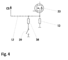
- Figure 4 presents one embodiment of a current sensing arrangement of a switched-mode power supply with power factor correction according to the present invention.
- a current sense input 12 connected from the source of the MOSFET 23 to the SMPS+PFC controller block 21.
- a first sense resistor 13 connected to the source of the MOSFET 23 of the current sensing arrangement of the presented embodiment.
- different current sense resistor values can be used for different voltage ranges by using sense resistor switch 39 to switch the second sense resistor 38 on to decrease the shunt resistance value for low input voltage range, where higher peak primary currents occur.
- the MOSFET 23 may e.g. be a low-Rds MOSFET 23.
- Figure 5 presents another embodiment of a circuit diagram of a switched-mode power supply with power factor correction according to the present invention.
- the presented another embodiment shows a boost stage of a two-stage PFC switched-mode power supply.
- the presented switched-mode power supply with power factor correction has a mains AC input block 1 and a diode bridge rectifier 7.
- the mains AC input voltage generated from the mains AC input block 1 is rectified in the diode bridge rectifier 7 to generate full-wave rectified input voltage 8.
- the presented switched-mode power supply with power factor correction has an SMPS+PFC controller block 21, a first MOSFET 22, a second MOSFET 23, an isolated transformer 40 and a primary capacitor 25.
- the said isolated transformer 40 may be a boost inductor 40 with a center tap 42 as a primary side midpoint 42.
- the first MOSFET 22 is connected from its drain to a primary side endpoint 41 of said boost inductor 40 and the second MOSFET 23 is connected from its drain to a primary side center tap 42 of said boost inductor 40.
- the term "primary side endpoint” specifies that all of the primary side winding of said boost inductor 40 is utilized in the coupling.
- the term "primary side midpoint” specifies that a specific portion of the primary side winding of said boost inductor 40 is utilized in the coupling, said specific portion of the primary side winding being 10 %- 75 %, preferably 30 %- 60 %, more preferably 50 % of the total primary side winding.
- the SMPS+PFC controller block 21 of the switched-mode power supply with power factor correction samples the rectified input voltage 8 (V fm ) from the diode bridge rectifier 7 and controls the switching of the first MOSFET 22 and the second MOSFET 23.
- a first primary capacitor 25 is needed as switching period power storage.
- the input voltage range is divided into two ranges.
- the switched-mode power supply with power factor correction according to the present another embodiment has a low-pass filter 28 and a voltage comparator block 29.
- the full-wave rectified input voltage 8 is filtered using the low-pass filter 28 to find out the peak value of the input voltage 8.
- the peak value of the input voltage 8 is used for the selection of the input voltage range.
- the selection of the input voltage range is done by the voltage comparator block 29, said voltage comparator block 29 having a reference voltage.
- the voltage comparator block 29 activates a first control signal 'A' at low voltages in a low input voltage range said first control signal 'A' switching the connection of the output of the SMPS+PFC controller block 21 to the gate of the second MOSFET 23. Respectively, the voltage comparator block 29 activates a second control signal 'B' at high voltages in a high input voltage range said second control signal 'B' switching the connection of the output of the SMPS+PFC controller block 21 to the gate of the first MOSFET 22.
- the first primary capacitor 25 in the input filter of the PFC supply represents the capacitance value used in the high voltage range.
- the first control signal 'A' activated by the voltage comparator block 29 may be used switch on a second primary capacitor 30 connected in parallel with the said first primary capacitor 25. Both the first primary capacitor 25 and the second primary capacitor 30 together represent the capacitance value used in the low voltage range.
- the output of the SMPS+PFC controller block 21 is connected to the gate of the first MOSFET 22 or to the gate of the second MOSFET 23 as switched by the first control signal 'A' and the second control signal 'B' activated by the voltage comparator block 29.
- the SMPS+PFC controller block 21 samples the rectified input voltage 8 (V fm ) and tries to create a similar waveform for the input current, so that the load introduced by the presented switched-mode power supply with power factor correction looks resistive.
- the SMPS+PFC controller block 21 has a current sense input 12 connected to the source of the first MOSFET 22 and to the source of the second MOSFET 23.
- the input voltage range is divided into two ranges, a low input voltage range and a high input voltage range.
- a larger capacitance of the primary filter and smaller primary inductance of the switching transformer are used for the low-end of the input voltage range.
- smaller capacitance and higher inductance are utilized at the high-end of the input voltage range.
- the first MOSFET 22 is connected from its drain to a primary side endpoint 41 of said boost inductor 40.
- Said first input capacitor 31 and said first input resistor 32 form a first primary side snubber for reducing EMI (EMI, electromagnetic interference).
- the second MOSFET 23 is connected from its drain to a primary side center tap 42 of said boost inductor 40.
- EMI electromagnetic interference
- the second MOSFET 23 is connected from its drain to a primary side center tap 42 of said boost inductor 40.
- Said second input capacitor 33 and said second input resistor 34 form a second primary side snubber for reducing EMI.
- the SMPS+PFC controller block 21 controls the switching of the first MOSFET 22 and the second MOSFET 23.
- the SMPS+PFC controller block 21 controls the switching of the first MOSFET 22 and provides the input current 35 from the drain of the first MOSFET 22 to the primary side endpoint 41 of said boost inductor 40.
- the SMPS+PFC controller block 21 controls the switching of the second MOSFET 23 and provides the input current 36 from the drain of the second MOSFET 23 to the primary side center tap 42 of said boost inductor 40.
- a switched-mode power supply with power factor correction there may be a series diode 37 coupled between the primary side endpoint 41 of said boost inductor 40 and the drain of the first MOSFET 22.
- the first MOSFET 22 utilizes the series diode 37 for preventing the current from flowing opposite way via the body diode when the second MOSFET 23 is operating.
- the secondary output of the boost inductor 40 of the presented switched-mode power supply with power factor correction according to the present another embodiment is connected to an output rectifier diode 43 and an output storage capacitor 44.
- the primary winding of said boost inductor 40 may be divided into two equal sections. Since the inductance of a coil is proportional to the second power of the number of turns, one half of the primary winding of said boost inductor 40 has one fourth of the inductance of total primary winding of said boost inductor 40.
- the inductance winding turn ratio between the two halves of the primary winding of said boost inductor 40 is freely selectable.
- the first MOSFET 22 used at high voltage range is connected from its drain to a primary side endpoint 41 of said boost inductor 40.
- the second MOSFET 23 is connected from its drain to a primary side center tap 42 of said boost inductor 40.
- the voltage comparator block 29 controls the selection of the first MOSFET 22 and the second MOSFET 23.
- the selected MOSFET 22, 23 is controlled by the SMPS+PFC controller block 21.
- the principle according to the present invention can also be used in DC-input power supplies, where very large input voltage range is desirable.
- the series diode 37 coupled between the primary side endpoint 41 of said boost inductor 40 and the drain of the first MOSFET 22 prevents the two MOSFETs 22, 23 connected to the primary side of said boost inductor 40 from creating a short circuit or other harmful situation even when conducting at the same time. Therefore, the switch between the MOSFETs 22, 23 can for example be a normal two-channel low-side driver with separate enable inputs and there are no timing requirements for the primary change.
- the SMPS+PFC controller block 21 sees a primary inductance of one fourth of the inductance of total of said boost inductor 40 at low voltage, compared to the inductance of total of said boost inductor 40 at high input voltage.
- the solution according to the present invention helps to optimize operation and voltage regulation over wide input voltage range. With help of the solution according to the present invention, the input voltage ranges of 1:9 can be reliably used.
- Switched-mode power supplies with power factor correction are promising solutions enabling the most efficient delivery of electrical power from the power company to the user.
- the input voltage dynamic range of a switched-mode power supply structure with power factor correction is sufficient for providing electrical power for both low-end and high-end input voltage ranges.
- the switched-mode power supply structure with power factor correction according to the present invention provides a reliable operation for the low-end input voltage range and also for the high-end input voltage range.
- the solution according to the present invention provides a simple and straight-forward switched-mode power supply structure with power factor correction that has a broader input voltage dynamic range than the prior art switched-mode power supplies with power factor correction.
Landscapes
- Engineering & Computer Science (AREA)
- Power Engineering (AREA)
- Dc-Dc Converters (AREA)
- Rectifiers (AREA)
Priority Applications (2)
| Application Number | Priority Date | Filing Date | Title |
|---|---|---|---|
| EP16195755.0A EP3316464B1 (fr) | 2016-10-26 | 2016-10-26 | Alimentation à découpage avec correction du facteur de puissance |
| PCT/EP2017/077217 WO2018077910A1 (fr) | 2016-10-26 | 2017-10-25 | Alimentation électrique à découpage dotée de correction de facteur de puissance |
Applications Claiming Priority (1)
| Application Number | Priority Date | Filing Date | Title |
|---|---|---|---|
| EP16195755.0A EP3316464B1 (fr) | 2016-10-26 | 2016-10-26 | Alimentation à découpage avec correction du facteur de puissance |
Publications (2)
| Publication Number | Publication Date |
|---|---|
| EP3316464A1 true EP3316464A1 (fr) | 2018-05-02 |
| EP3316464B1 EP3316464B1 (fr) | 2020-04-08 |
Family
ID=57206150
Family Applications (1)
| Application Number | Title | Priority Date | Filing Date |
|---|---|---|---|
| EP16195755.0A Active EP3316464B1 (fr) | 2016-10-26 | 2016-10-26 | Alimentation à découpage avec correction du facteur de puissance |
Country Status (2)
| Country | Link |
|---|---|
| EP (1) | EP3316464B1 (fr) |
| WO (1) | WO2018077910A1 (fr) |
Citations (5)
| Publication number | Priority date | Publication date | Assignee | Title |
|---|---|---|---|---|
| EP0726640A2 (fr) * | 1995-02-10 | 1996-08-14 | Kabushiki Kaisha Toshiba | Circuit convertiseur alternatif-continu pour alimentation de puissance |
| WO2009105734A2 (fr) * | 2008-02-22 | 2009-08-27 | Murata Power Solutions | Procédé et appareil pour conversion d’alimentation avec plage de tension d’entrée large |
| US7729135B1 (en) * | 2007-05-10 | 2010-06-01 | Fairchild Semiconductor Corporation | Power converter using a single tapped transformer for multiple ranges of input voltage |
| WO2011116942A2 (fr) * | 2010-03-23 | 2011-09-29 | Sagem Defense Securite | Convertisseur alternatif/continu a isolement galvanique |
| US20130250625A1 (en) * | 2012-03-26 | 2013-09-26 | Murata Manufacturing Co., Ltd. | Switching power supply apparatus |
Family Cites Families (3)
| Publication number | Priority date | Publication date | Assignee | Title |
|---|---|---|---|---|
| CN201127004Y (zh) * | 2007-12-07 | 2008-10-01 | 深圳市同洲电子股份有限公司 | 一种开关电源电路及线性变压电路 |
| US20130235623A1 (en) * | 2012-03-12 | 2013-09-12 | System General Corp. | Two-switch flyback power converters |
| DE202013102618U1 (de) * | 2013-06-18 | 2014-09-19 | Weidmüller Interface GmbH & Co. KG | Netzteil, insbesondere Weitbereichsnetzteil |
-
2016
- 2016-10-26 EP EP16195755.0A patent/EP3316464B1/fr active Active
-
2017
- 2017-10-25 WO PCT/EP2017/077217 patent/WO2018077910A1/fr not_active Ceased
Patent Citations (5)
| Publication number | Priority date | Publication date | Assignee | Title |
|---|---|---|---|---|
| EP0726640A2 (fr) * | 1995-02-10 | 1996-08-14 | Kabushiki Kaisha Toshiba | Circuit convertiseur alternatif-continu pour alimentation de puissance |
| US7729135B1 (en) * | 2007-05-10 | 2010-06-01 | Fairchild Semiconductor Corporation | Power converter using a single tapped transformer for multiple ranges of input voltage |
| WO2009105734A2 (fr) * | 2008-02-22 | 2009-08-27 | Murata Power Solutions | Procédé et appareil pour conversion d’alimentation avec plage de tension d’entrée large |
| WO2011116942A2 (fr) * | 2010-03-23 | 2011-09-29 | Sagem Defense Securite | Convertisseur alternatif/continu a isolement galvanique |
| US20130250625A1 (en) * | 2012-03-26 | 2013-09-26 | Murata Manufacturing Co., Ltd. | Switching power supply apparatus |
Also Published As
| Publication number | Publication date |
|---|---|
| EP3316464B1 (fr) | 2020-04-08 |
| WO2018077910A1 (fr) | 2018-05-03 |
Similar Documents
| Publication | Publication Date | Title |
|---|---|---|
| US8693213B2 (en) | Resonant power factor correction converter | |
| EP1735901B1 (fr) | Convertisseur ca/cc comprenant une pluralite de convertisseurs montes en cascade | |
| US10833594B2 (en) | System and method of controlling a power converter having an LC tank coupled between a switching network and a transformer winding | |
| US5233509A (en) | Switch-mode AC-to-DC converter | |
| US6021052A (en) | DC/AC power converter | |
| US8102678B2 (en) | High power factor isolated buck-type power factor correction converter | |
| US6005780A (en) | Single-stage AC/DC conversion with PFC-tapped transformers | |
| US6344986B1 (en) | Topology and control method for power factor correction | |
| US5894412A (en) | System with open-loop DC-DC converter stage | |
| CA2971883C (fr) | Convertisseur a transfert indirect | |
| US5734562A (en) | Power factor correction circuit | |
| EP2339727A1 (fr) | Circuit de correction du facteur de puissance à étage unique, avec un commutateur unique et sortie isolée et utilisant un inducteur élévateur entre une source CA et un rectificateur de pont | |
| US9401653B2 (en) | Power supply with switching converter | |
| CN102668352B (zh) | 带有功率因数校正的转换器 | |
| Naraharisetti et al. | Design and modeling of CCM average current control PFC AC-DC Boost converter | |
| US8711588B1 (en) | Power supply device | |
| CN102630368B (zh) | 具有功率因数校正的通量转换器 | |
| Das et al. | Design of Flyback converter by using an ideal switch and a MOSFET switch | |
| US6697269B2 (en) | Single-stage converter compensating power factor | |
| EP3316464B1 (fr) | Alimentation à découpage avec correction du facteur de puissance | |
| Zhao et al. | A seven-level switched capacitor ac-dc rectifier for fast wireless charging | |
| US20020101743A1 (en) | Power line separator | |
| JPH0723560A (ja) | スイッチング電源 | |
| Tonolo et al. | An Interleaved Current-Fed PFC Flyback Converter With Voltage Follower Characteristic | |
| Dagur et al. | Single Phase AC-DC Converter employing Power Factor Correction with High Frequency Isolation Using Buck-Boost PWM Converter |
Legal Events
| Date | Code | Title | Description |
|---|---|---|---|
| PUAI | Public reference made under article 153(3) epc to a published international application that has entered the european phase |
Free format text: ORIGINAL CODE: 0009012 |
|
| STAA | Information on the status of an ep patent application or granted ep patent |
Free format text: STATUS: THE APPLICATION HAS BEEN PUBLISHED |
|
| AK | Designated contracting states |
Kind code of ref document: A1 Designated state(s): AL AT BE BG CH CY CZ DE DK EE ES FI FR GB GR HR HU IE IS IT LI LT LU LV MC MK MT NL NO PL PT RO RS SE SI SK SM TR |
|
| AX | Request for extension of the european patent |
Extension state: BA ME |
|
| STAA | Information on the status of an ep patent application or granted ep patent |
Free format text: STATUS: REQUEST FOR EXAMINATION WAS MADE |
|
| 17P | Request for examination filed |
Effective date: 20181029 |
|
| RBV | Designated contracting states (corrected) |
Designated state(s): AL AT BE BG CH CY CZ DE DK EE ES FI FR GB GR HR HU IE IS IT LI LT LU LV MC MK MT NL NO PL PT RO RS SE SI SK SM TR |
|
| GRAP | Despatch of communication of intention to grant a patent |
Free format text: ORIGINAL CODE: EPIDOSNIGR1 |
|
| STAA | Information on the status of an ep patent application or granted ep patent |
Free format text: STATUS: GRANT OF PATENT IS INTENDED |
|
| INTG | Intention to grant announced |
Effective date: 20191115 |
|
| GRAS | Grant fee paid |
Free format text: ORIGINAL CODE: EPIDOSNIGR3 |
|
| GRAA | (expected) grant |
Free format text: ORIGINAL CODE: 0009210 |
|
| STAA | Information on the status of an ep patent application or granted ep patent |
Free format text: STATUS: THE PATENT HAS BEEN GRANTED |
|
| AK | Designated contracting states |
Kind code of ref document: B1 Designated state(s): AL AT BE BG CH CY CZ DE DK EE ES FI FR GB GR HR HU IE IS IT LI LT LU LV MC MK MT NL NO PL PT RO RS SE SI SK SM TR |
|
| RAP1 | Party data changed (applicant data changed or rights of an application transferred) |
Owner name: ABB SCHWEIZ AG |
|
| REG | Reference to a national code |
Ref country code: CH Ref legal event code: EP Ref country code: AT Ref legal event code: REF Ref document number: 1255699 Country of ref document: AT Kind code of ref document: T Effective date: 20200415 |
|
| REG | Reference to a national code |
Ref country code: DE Ref legal event code: R096 Ref document number: 602016033437 Country of ref document: DE |
|
| REG | Reference to a national code |
Ref country code: IE Ref legal event code: FG4D |
|
| REG | Reference to a national code |
Ref country code: FI Ref legal event code: FGE |
|
| REG | Reference to a national code |
Ref country code: NL Ref legal event code: MP Effective date: 20200408 |
|
| REG | Reference to a national code |
Ref country code: LT Ref legal event code: MG4D |
|
| PG25 | Lapsed in a contracting state [announced via postgrant information from national office to epo] |
Ref country code: GR Free format text: LAPSE BECAUSE OF FAILURE TO SUBMIT A TRANSLATION OF THE DESCRIPTION OR TO PAY THE FEE WITHIN THE PRESCRIBED TIME-LIMIT Effective date: 20200709 Ref country code: NO Free format text: LAPSE BECAUSE OF FAILURE TO SUBMIT A TRANSLATION OF THE DESCRIPTION OR TO PAY THE FEE WITHIN THE PRESCRIBED TIME-LIMIT Effective date: 20200708 Ref country code: PT Free format text: LAPSE BECAUSE OF FAILURE TO SUBMIT A TRANSLATION OF THE DESCRIPTION OR TO PAY THE FEE WITHIN THE PRESCRIBED TIME-LIMIT Effective date: 20200817 Ref country code: NL Free format text: LAPSE BECAUSE OF FAILURE TO SUBMIT A TRANSLATION OF THE DESCRIPTION OR TO PAY THE FEE WITHIN THE PRESCRIBED TIME-LIMIT Effective date: 20200408 Ref country code: LT Free format text: LAPSE BECAUSE OF FAILURE TO SUBMIT A TRANSLATION OF THE DESCRIPTION OR TO PAY THE FEE WITHIN THE PRESCRIBED TIME-LIMIT Effective date: 20200408 Ref country code: IS Free format text: LAPSE BECAUSE OF FAILURE TO SUBMIT A TRANSLATION OF THE DESCRIPTION OR TO PAY THE FEE WITHIN THE PRESCRIBED TIME-LIMIT Effective date: 20200808 Ref country code: SE Free format text: LAPSE BECAUSE OF FAILURE TO SUBMIT A TRANSLATION OF THE DESCRIPTION OR TO PAY THE FEE WITHIN THE PRESCRIBED TIME-LIMIT Effective date: 20200408 |
|
| REG | Reference to a national code |
Ref country code: AT Ref legal event code: MK05 Ref document number: 1255699 Country of ref document: AT Kind code of ref document: T Effective date: 20200408 |
|
| PG25 | Lapsed in a contracting state [announced via postgrant information from national office to epo] |
Ref country code: HR Free format text: LAPSE BECAUSE OF FAILURE TO SUBMIT A TRANSLATION OF THE DESCRIPTION OR TO PAY THE FEE WITHIN THE PRESCRIBED TIME-LIMIT Effective date: 20200408 Ref country code: LV Free format text: LAPSE BECAUSE OF FAILURE TO SUBMIT A TRANSLATION OF THE DESCRIPTION OR TO PAY THE FEE WITHIN THE PRESCRIBED TIME-LIMIT Effective date: 20200408 Ref country code: RS Free format text: LAPSE BECAUSE OF FAILURE TO SUBMIT A TRANSLATION OF THE DESCRIPTION OR TO PAY THE FEE WITHIN THE PRESCRIBED TIME-LIMIT Effective date: 20200408 Ref country code: BG Free format text: LAPSE BECAUSE OF FAILURE TO SUBMIT A TRANSLATION OF THE DESCRIPTION OR TO PAY THE FEE WITHIN THE PRESCRIBED TIME-LIMIT Effective date: 20200708 |
|
| PG25 | Lapsed in a contracting state [announced via postgrant information from national office to epo] |
Ref country code: AL Free format text: LAPSE BECAUSE OF FAILURE TO SUBMIT A TRANSLATION OF THE DESCRIPTION OR TO PAY THE FEE WITHIN THE PRESCRIBED TIME-LIMIT Effective date: 20200408 |
|
| REG | Reference to a national code |
Ref country code: DE Ref legal event code: R097 Ref document number: 602016033437 Country of ref document: DE |
|
| PG25 | Lapsed in a contracting state [announced via postgrant information from national office to epo] |
Ref country code: ES Free format text: LAPSE BECAUSE OF FAILURE TO SUBMIT A TRANSLATION OF THE DESCRIPTION OR TO PAY THE FEE WITHIN THE PRESCRIBED TIME-LIMIT Effective date: 20200408 Ref country code: CZ Free format text: LAPSE BECAUSE OF FAILURE TO SUBMIT A TRANSLATION OF THE DESCRIPTION OR TO PAY THE FEE WITHIN THE PRESCRIBED TIME-LIMIT Effective date: 20200408 Ref country code: SM Free format text: LAPSE BECAUSE OF FAILURE TO SUBMIT A TRANSLATION OF THE DESCRIPTION OR TO PAY THE FEE WITHIN THE PRESCRIBED TIME-LIMIT Effective date: 20200408 Ref country code: RO Free format text: LAPSE BECAUSE OF FAILURE TO SUBMIT A TRANSLATION OF THE DESCRIPTION OR TO PAY THE FEE WITHIN THE PRESCRIBED TIME-LIMIT Effective date: 20200408 Ref country code: AT Free format text: LAPSE BECAUSE OF FAILURE TO SUBMIT A TRANSLATION OF THE DESCRIPTION OR TO PAY THE FEE WITHIN THE PRESCRIBED TIME-LIMIT Effective date: 20200408 Ref country code: EE Free format text: LAPSE BECAUSE OF FAILURE TO SUBMIT A TRANSLATION OF THE DESCRIPTION OR TO PAY THE FEE WITHIN THE PRESCRIBED TIME-LIMIT Effective date: 20200408 Ref country code: DK Free format text: LAPSE BECAUSE OF FAILURE TO SUBMIT A TRANSLATION OF THE DESCRIPTION OR TO PAY THE FEE WITHIN THE PRESCRIBED TIME-LIMIT Effective date: 20200408 |
|
| PLBE | No opposition filed within time limit |
Free format text: ORIGINAL CODE: 0009261 |
|
| STAA | Information on the status of an ep patent application or granted ep patent |
Free format text: STATUS: NO OPPOSITION FILED WITHIN TIME LIMIT |
|
| PG25 | Lapsed in a contracting state [announced via postgrant information from national office to epo] |
Ref country code: SK Free format text: LAPSE BECAUSE OF FAILURE TO SUBMIT A TRANSLATION OF THE DESCRIPTION OR TO PAY THE FEE WITHIN THE PRESCRIBED TIME-LIMIT Effective date: 20200408 Ref country code: PL Free format text: LAPSE BECAUSE OF FAILURE TO SUBMIT A TRANSLATION OF THE DESCRIPTION OR TO PAY THE FEE WITHIN THE PRESCRIBED TIME-LIMIT Effective date: 20200408 |
|
| 26N | No opposition filed |
Effective date: 20210112 |
|
| PG25 | Lapsed in a contracting state [announced via postgrant information from national office to epo] |
Ref country code: SI Free format text: LAPSE BECAUSE OF FAILURE TO SUBMIT A TRANSLATION OF THE DESCRIPTION OR TO PAY THE FEE WITHIN THE PRESCRIBED TIME-LIMIT Effective date: 20200408 |
|
| REG | Reference to a national code |
Ref country code: CH Ref legal event code: PL |
|
| GBPC | Gb: european patent ceased through non-payment of renewal fee |
Effective date: 20201026 |
|
| PG25 | Lapsed in a contracting state [announced via postgrant information from national office to epo] |
Ref country code: LU Free format text: LAPSE BECAUSE OF NON-PAYMENT OF DUE FEES Effective date: 20201026 Ref country code: MC Free format text: LAPSE BECAUSE OF FAILURE TO SUBMIT A TRANSLATION OF THE DESCRIPTION OR TO PAY THE FEE WITHIN THE PRESCRIBED TIME-LIMIT Effective date: 20200408 |
|
| REG | Reference to a national code |
Ref country code: BE Ref legal event code: MM Effective date: 20201031 |
|
| PG25 | Lapsed in a contracting state [announced via postgrant information from national office to epo] |
Ref country code: BE Free format text: LAPSE BECAUSE OF NON-PAYMENT OF DUE FEES Effective date: 20201031 Ref country code: CH Free format text: LAPSE BECAUSE OF NON-PAYMENT OF DUE FEES Effective date: 20201031 Ref country code: LI Free format text: LAPSE BECAUSE OF NON-PAYMENT OF DUE FEES Effective date: 20201031 Ref country code: GB Free format text: LAPSE BECAUSE OF NON-PAYMENT OF DUE FEES Effective date: 20201026 |
|
| PG25 | Lapsed in a contracting state [announced via postgrant information from national office to epo] |
Ref country code: IE Free format text: LAPSE BECAUSE OF NON-PAYMENT OF DUE FEES Effective date: 20201026 |
|
| PG25 | Lapsed in a contracting state [announced via postgrant information from national office to epo] |
Ref country code: TR Free format text: LAPSE BECAUSE OF FAILURE TO SUBMIT A TRANSLATION OF THE DESCRIPTION OR TO PAY THE FEE WITHIN THE PRESCRIBED TIME-LIMIT Effective date: 20200408 Ref country code: MT Free format text: LAPSE BECAUSE OF FAILURE TO SUBMIT A TRANSLATION OF THE DESCRIPTION OR TO PAY THE FEE WITHIN THE PRESCRIBED TIME-LIMIT Effective date: 20200408 Ref country code: CY Free format text: LAPSE BECAUSE OF FAILURE TO SUBMIT A TRANSLATION OF THE DESCRIPTION OR TO PAY THE FEE WITHIN THE PRESCRIBED TIME-LIMIT Effective date: 20200408 |
|
| PG25 | Lapsed in a contracting state [announced via postgrant information from national office to epo] |
Ref country code: MK Free format text: LAPSE BECAUSE OF FAILURE TO SUBMIT A TRANSLATION OF THE DESCRIPTION OR TO PAY THE FEE WITHIN THE PRESCRIBED TIME-LIMIT Effective date: 20200408 |
|
| PGFP | Annual fee paid to national office [announced via postgrant information from national office to epo] |
Ref country code: DE Payment date: 20251021 Year of fee payment: 10 |
|
| PGFP | Annual fee paid to national office [announced via postgrant information from national office to epo] |
Ref country code: FI Payment date: 20251028 Year of fee payment: 10 Ref country code: IT Payment date: 20251024 Year of fee payment: 10 |
|
| PGFP | Annual fee paid to national office [announced via postgrant information from national office to epo] |
Ref country code: FR Payment date: 20251030 Year of fee payment: 10 |