EP3316481A1 - Circuit d'amplificateur de bande de base - Google Patents
Circuit d'amplificateur de bande de base Download PDFInfo
- Publication number
- EP3316481A1 EP3316481A1 EP16306434.8A EP16306434A EP3316481A1 EP 3316481 A1 EP3316481 A1 EP 3316481A1 EP 16306434 A EP16306434 A EP 16306434A EP 3316481 A1 EP3316481 A1 EP 3316481A1
- Authority
- EP
- European Patent Office
- Prior art keywords
- component
- differential
- boosted
- node
- baseband
- Prior art date
- Legal status (The legal status is an assumption and is not a legal conclusion. Google has not performed a legal analysis and makes no representation as to the accuracy of the status listed.)
- Withdrawn
Links
- 230000004044 response Effects 0.000 claims abstract description 18
- 238000001914 filtration Methods 0.000 claims description 7
- 230000003321 amplification Effects 0.000 claims description 6
- 238000003199 nucleic acid amplification method Methods 0.000 claims description 6
- 239000004065 semiconductor Substances 0.000 claims description 5
- 238000006243 chemical reaction Methods 0.000 claims description 4
- 230000005669 field effect Effects 0.000 claims description 4
- 229910044991 metal oxide Inorganic materials 0.000 claims description 4
- 150000004706 metal oxides Chemical class 0.000 claims description 4
- 238000010586 diagram Methods 0.000 description 11
- 230000006835 compression Effects 0.000 description 5
- 238000007906 compression Methods 0.000 description 5
- 238000012986 modification Methods 0.000 description 3
- 230000004048 modification Effects 0.000 description 3
- 230000008901 benefit Effects 0.000 description 2
- 230000002457 bidirectional effect Effects 0.000 description 2
- 230000008859 change Effects 0.000 description 2
- 230000009467 reduction Effects 0.000 description 2
- 230000000903 blocking effect Effects 0.000 description 1
- 238000000354 decomposition reaction Methods 0.000 description 1
- 230000001419 dependent effect Effects 0.000 description 1
- 230000006870 function Effects 0.000 description 1
- 238000012913 prioritisation Methods 0.000 description 1
- 230000002123 temporal effect Effects 0.000 description 1
Images


Classifications
-
- H—ELECTRICITY
- H03—ELECTRONIC CIRCUITRY
- H03F—AMPLIFIERS
- H03F1/00—Details of amplifiers with only discharge tubes, only semiconductor devices or only unspecified devices as amplifying elements
- H03F1/02—Modifications of amplifiers to raise the efficiency, e.g. gliding Class A stages, use of an auxiliary oscillation
- H03F1/0205—Modifications of amplifiers to raise the efficiency, e.g. gliding Class A stages, use of an auxiliary oscillation in transistor amplifiers
- H03F1/0261—Modifications of amplifiers to raise the efficiency, e.g. gliding Class A stages, use of an auxiliary oscillation in transistor amplifiers with control of the polarisation voltage or current, e.g. gliding Class A
-
- H—ELECTRICITY
- H03—ELECTRONIC CIRCUITRY
- H03H—IMPEDANCE NETWORKS, e.g. RESONANT CIRCUITS; RESONATORS
- H03H11/00—Networks using active elements
- H03H11/02—Multiple-port networks
- H03H11/32—Networks for transforming balanced signals into unbalanced signals and vice versa, e.g. baluns
-
- H—ELECTRICITY
- H03—ELECTRONIC CIRCUITRY
- H03F—AMPLIFIERS
- H03F3/00—Amplifiers with only discharge tubes or only semiconductor devices as amplifying elements
- H03F3/45—Differential amplifiers
- H03F3/45071—Differential amplifiers with semiconductor devices only
- H03F3/45076—Differential amplifiers with semiconductor devices only characterised by the way of implementation of the active amplifying circuit in the differential amplifier
- H03F3/4508—Differential amplifiers with semiconductor devices only characterised by the way of implementation of the active amplifying circuit in the differential amplifier using bipolar transistors as the active amplifying circuit
- H03F3/45085—Long tailed pairs
- H03F3/45089—Non-folded cascode stages
-
- G—PHYSICS
- G01—MEASURING; TESTING
- G01S—RADIO DIRECTION-FINDING; RADIO NAVIGATION; DETERMINING DISTANCE OR VELOCITY BY USE OF RADIO WAVES; LOCATING OR PRESENCE-DETECTING BY USE OF THE REFLECTION OR RERADIATION OF RADIO WAVES; ANALOGOUS ARRANGEMENTS USING OTHER WAVES
- G01S7/00—Details of systems according to groups G01S13/00, G01S15/00, G01S17/00
- G01S7/02—Details of systems according to groups G01S13/00, G01S15/00, G01S17/00 of systems according to group G01S13/00
-
- H—ELECTRICITY
- H03—ELECTRONIC CIRCUITRY
- H03F—AMPLIFIERS
- H03F3/00—Amplifiers with only discharge tubes or only semiconductor devices as amplifying elements
- H03F3/189—High-frequency amplifiers, e.g. radio frequency amplifiers
- H03F3/19—High-frequency amplifiers, e.g. radio frequency amplifiers with semiconductor devices only
- H03F3/195—High-frequency amplifiers, e.g. radio frequency amplifiers with semiconductor devices only in integrated circuits
-
- H—ELECTRICITY
- H03—ELECTRONIC CIRCUITRY
- H03F—AMPLIFIERS
- H03F3/00—Amplifiers with only discharge tubes or only semiconductor devices as amplifying elements
- H03F3/26—Push-pull amplifiers; Phase-splitters therefor
-
- H—ELECTRICITY
- H03—ELECTRONIC CIRCUITRY
- H03F—AMPLIFIERS
- H03F3/00—Amplifiers with only discharge tubes or only semiconductor devices as amplifying elements
- H03F3/45—Differential amplifiers
Definitions
- This invention relates to a baseband amplifier circuit, and in particular to a low-noise baseband amplifier circuit.
- a conventional wireless radio frequency (RF) receiver frontend topology comprises a low noise amplifier (LNA) arranged to amplifier signals received by an antenna, an active mixer (e.g. a Gilbert-type mixer) arranged to down-convert the amplified signals to a baseband frequency. Baseband filtering and variable gain amplification is then performed.
- LNA low noise amplifier
- active mixer e.g. a Gilbert-type mixer
- Such a conventional RF receiver topology achieves good noise performance, but may eventually suffer from a poor compression point depending on the input signal level power.
- Radar receivers such as used within automotive advanced driver assistance systems, require both good noise and good compression point performance, and an acceptable trade-off using conventional receiver topologies is difficult to reach.
- radar receivers often use a different topology receiver frontend topology in which an unamplified signal received by the antenna is provided directly to the active mixer. By removing the LNA a better trade-off between noise and compression point can be achieved.
- the achievable receiver noise performance is limited, due mainly to the noise contribution of the active mixer because the mixer noise is not masked by any gain stage preceding it.
- the present invention provides a baseband amplifier circuit and a radio frequency frontend module as described in the accompanying claims.
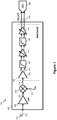
- FIG. 1 there is schematically illustrated a simplified block diagram of an example embodiment of an RF receiver frontend module 100, which in the illustrated example is implemented within an integrated circuit device 105.
- An input of the RF receiver frontend module 100 is arranged to be coupled to an antenna 110.
- the RF receiver frontend module 100 comprises a low noise amplifier (LNA) component 120 to which an RF signal 112 received from the antenna 110 is provided.
- LNA low noise amplifier
- band pass filtering may be applied to the received RF signal 112 before being provided to the LNA component 120.
- the LNA component 120 amplifies the received RF signal 112, and outputs the amplified RF signal 125 to a single-ended passive mixer component 130 which mixes the amplified RF signal 125 with a conversion signal, which in the illustrated example comprises a local oscillator signal 115, to down-convert the amplified RF signal 125 to a baseband frequency signal 135.
- the baseband frequency signal 135 is then provided to a baseband component 140 in which baseband filtering and variable gain amplification is then performed. In the illustrated example such baseband filtering and variable gain amplification is performed by a series of high-pass filter components 160 and variable gain amplifiers 170.
- the baseband component 140 then outputs a baseband signal 145, which may be provided to an analogue to digital converter (ADC) 180 for further (digital) processing.
- ADC analogue to digital converter
- the baseband component 140 of the illustrated example further comprises a baseband (ultra) low-noise amplifier 150 arranged to receive the single-ended baseband frequency signal 135 output by the passive mixer component 130 and output an amplified baseband frequency signal 155 to which the baseband filtering and variable gain amplification is then performed, which in the illustrated example comprises a differential baseband frequency signal 155.
- a baseband (ultra) low-noise amplifier 150 arranged to receive the single-ended baseband frequency signal 135 output by the passive mixer component 130 and output an amplified baseband frequency signal 155 to which the baseband filtering and variable gain amplification is then performed, which in the illustrated example comprises a differential baseband frequency signal 155.
- the baseband low-noise amplifier 150 By providing the baseband low-noise amplifier 150 to amplify the baseband frequency signal, an acceptable gain for the received signal may be achieved. In order to achieve good noise performance of the baseband signal 145 output by the baseband component 140, the performance of the baseband amplifier 150 is of high importance.
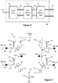
- the baseband amplifier circuit 150 of Figure 2 comprises a single-ended to differential converter 200 arranged to receive at an input thereof a single-ended input signal to be amplified, such as the single-ended baseband frequency signal 135 output by the passive mixer component 130 of the RF receiver frontend module 100 of Figure 1 , and to convert the single-ended input signal 135 into a differential signal 205.
- the baseband amplifier circuit 150 of Figure 2 further comprises a series of n (i.e. one or more) amplifier module(s), coupled one after the other (output to input as illustrated in Figure 2 ) when n > 1.
- each amplifier module comprises a boosted follower amplifier 210 arranged to receive at a differential input thereof a differential signal 205, 215 to be amplified and to output an amplified differential signal 215, 155 based on the received differential input signal 205, 215.
- a first boosted follower amplifier component 210 is arranged to receive the differential signal 205 output by the single-ended to differential converter 200, whilst each subsequent boosted follower amplifier component 210 within the series is arranged to receive the differential signals 215 output by the preceding boosted follower amplifier component 210 within the series.
- the amplified differential signal 155 output by a last boosted follower amplifier component 210 may the form the basis of (or constitute) the amplified baseband frequency signal 155 to which baseband filtering and variable gain amplification is subsequently performed within the baseband component 140 of the RF receiver frontend module 100 of Figure 1 .
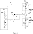
- FIG 3 schematically illustrates a simplified circuit diagram of an example of a boosted follower amplifier component 210 such as may be used to implement the boosted follower amplifier components 210 illustrated in Figure 2 .
- the boosted follower amplifier component 210 illustrated in Figure 3 comprises four transconductance devices 310 - 340, which in the illustrated example are implemented by way of bipolar junction transistors. However, it is contemplated that the transconductance devices 310 - 340 may be implemented using other devices, for example metal oxide semiconductor field effect transistors or the like.
- a first transconductance device 310 is arranged to control a first current 315 between a first supply node 300 and a first output node 350 of the boosted follower amplifier component 210 in response to a voltage at an input terminal 312 thereof.
- the input terminal 312 of the first transconductance device 310 is coupled to a first input node 360 of the boosted follower amplifier component 210.
- a second transconductance device 320 is arranged to control a second current 325 between the first output node 350 of the boosted follower amplifier component 210 and a second supply node 305 in response to a voltage at an input terminal 325 thereof.
- the input terminal 322 of the second transconductance device 320 is coupled to a second input node 362 of the boosted follower amplifier component 210.
- a third transconductance device 330 is arranged to control a third current 335 between the first supply node 300 and a second output node 355 of the boosted follower amplifier component 210 in response to a voltage at an input terminal 332 thereof.
- the input terminal 332 of the third transconductance device 330 is coupled to a third input node 364 of the boosted follower amplifier component 210.
- a fourth transconductance device 340 is arranged to control a fourth current 345 between the second output node 355 of the boosted follower amplifier component 210 and the second supply node 305 in response to a voltage at an input terminal 342 thereof.
- the input terminal 342 of the fourth transconductance device 340 is coupled to a fourth input node 366 of the boosted follower amplifier component 210.
- the first and third input nodes 360, 364 of the boosted follower amplifier component 210 are arranged to receive a first (positive) component Vin_p of the received differential input signal 205, 215 and the second and further input nodes 362, 366 of the boosted follower amplifier component 210 are arranged to receive a second (negative) component Vin_n of the received differential input signal 205, 215.
- the boosted follower amplifier component 210 illustrated in Figure 2 comprises stacked pairs of cross-coupled transconductance devices 310 - 340.
- the stacked first and second transconductance devices 310, 320 operate as a gm2 ⁇ Zload buffer, where Zload represents an impedance of a load of the second transconductance device 320.
- Zload may be defined as 1/gm1, where gm1 is a transductance of the first transconductance device 310 (gm2 being a transductance of the second transconductance device 320, gm3 being a transductance of the third transconductance device 330 and gm4 being a transductance of the fourth transconductance device 340).
- the term 'transductance' may generally be used for designating a ratio of a current change ⁇ Iout at an output of the respective transconductance device to a voltage change ⁇ Vin at an input port of the respective transconductance device.
- 'beta' may be used for designating a common-emitter current gain, which may be approximately the ratio of a DC collector current to a DC base current in forward-active region of a bipolar transistor.
- a gain of the stacked third and fourth transconductance devices 330, 340 may be defined as gm4 ⁇ 1/gm3.
- a 2* gain (corresponding to 6 dB) may be achieved.
- the gain at each output node 350, 355 is defined by the transconductance (gm * 1/gm) of the respective transconductance devices. Accordingly, the gain of the boosted follower amplifier component 210 illustrated in Figure 3 is independent of the magnitude of the bias currents 315 - 345 through the transconductance devices for low to mid frequencies (e.g. up to 10 GHz).
- a 2x gain may be achieved without increasing the current consumption of the amplifier circuit, and whilst enabling good noise performance and broadband behaviour of the amplifier.
- the bias current may be increased for maintaining or achieving a gain G of about 6 dB.
- the boosted follower amplifier component 210 further comprises a current source 370 coupled to the second supply node 305 and arranged to absorb the combined second and fourth currents 325, 345.
- the current sources 370 may be implemented by a simple resistance, or even omitted in very low voltage operation.
- a current source may alternatively be coupled to the first supply node 300 and arranged to supply the combined first and third currents 315, 335.
- the boosted follower amplifier component 210 illustrated in Figure 3 further comprises DC (direct current) decoupling components coupled between the input nodes 360,, 362, 364, 366 and the transconductance devices 310 - 340.
- each DC decoupling component comprises an RC filter comprising a capacitance 380 coupled between the respective input node 360, 365 of the boosted follower amplifier component 210 and the input terminal 312, 322, 332, 342 of the respective transconductance device 310 - 340, and a resistance 385 coupled between the input terminal 312, 322, 332, 342 of the respective transconductance device 310 - 340 and a bias voltage node 387, 389.
- the resistance 385 of the DC decoupling components coupled to the input terminals 312, 332 of the first and third transconductance devices 310, 330 may be coupled to a first (e.g. higher) bias voltage node 387, and the resistance 385 of the DC decoupling components coupled to the input terminals 322, 342 of the second and fourth transconductance devices 320, 340 may be coupled to a second (e.g. lower) bias voltage node 389.
- the single-ended to differential converter 200 illustrated in Figure 4 comprises a transconductance device 400 arranged to control a current 410 between a third supply node 420 and a fourth supply node 425 in response to a voltage at an input terminal 402 thereof coupled to an input node 430 of the single-ended to differential converter.
- the transconductance device 440 comprises a bipolar junction transistor device.
- the transconductance device 400 may be implemented using another type of device, for example a metal oxide semiconductor field effect transistor or the like.
- the single-ended to differential converter 200 further comprises a first resistance component 440 coupled between the transconductance device 400 and the third supply node 420, and a second resistance component 445coupled between the transconductance device 410 and the fourth supply node 425.
- each of the resistance components 440, 445 comprises a base-collector shorted bipolar junction transistor device 442 coupled in series with a resistive element 444.
- the base-collector shorted bipolar junction transistor devices 442 limit the current 410 (and thus the current consumption of the circuit while enabling low value resistance elements 44, and thus low noise.
- the single-ended to differential converter 200 further comprises a DC decoupling component coupled between the input node 43 of the single-ended to differential converter 200 and the transconductance device 400.
- the DC decoupling component comprises an RC filter comprising a capacitance 450 coupled between the input node 430 of the single-ended to differential converter 200 and the input terminal of the transconductance device 400, and a resistance 455 coupled between the input terminal of the transconductance device 400 and a bias voltage node 457.
- a bias circuit 460 may be arranged to generate a bias voltage at the bias node 457 for biasing a DC voltage of the input terminal 342 of the transconductance device 400.
- the RC filter may be arranged to comprise a cut-off frequency less than the high-pass filter components 160 of the receiver frontend baseband component 140 illustrated in Figure 1 .
- a baseband low-noise amplifier 150 comprising a single-ended to differential converter 200 and one or more boosted follower amplifier component 210.
- the gain of the example boosted follower amplifier 210 illustrated in Figure 3 is independent of its bias current, and the combined arrangement of the single-ended to differential converter 200 and boosted follower amplifier component(s) 210 takes advantage of the non-correlation between the gain and current drain of the boosted follower amplifier topology, and of its low noise performance, while providing a single to differential active conversion.
- the current limiting influence of the base-collector shorted bipolar transistors 442 of the single-ended to differential converter 200 illustrated in Figure 4 allows interfacing with the output of the single-ended mixer 130 of the receiver front-end 100 illustrated in Figure 1 , while preserving the low noise and broadband behaviour of the boosted follower amplifier component(s) 210.
- the present invention is not limited to the specific single-ended to differential converter 200 illustrated in Figure 4 .
- any active single ended to differential converter with current limiting devices e.g.
- diodes, resistors, etc. may permit interfacing with the output of the single-ended mixer 130 of the receiver front-end 100 illustrated in Figure 1 , while (at least partially) preserving the low noise and broadband behaviour of the boosted follower amplifier component(s) 210.
- the exemplary embodiment hereinbefore described enables outstanding noise performance to be achieved as compared to state of the art arrangements, while preserving low power consumption and also being capable of being integrated into a single semiconductor device.
- the baseband amplifier circuit herein described enables the range of an RF radar system in which it is implemented to be significantly increased.
- the number n of boosted follower amplifier components implemented within the baseband amplifier circuit may vary depending on the specific application, and in particular may depend on a desired trade-off between noise, compression point, bandwidth and power consumption.
- FIG. 5 schematically illustrates a simplified block diagram of an alternative example of a baseband amplifier circuit 150 such as may be used to implement the baseband amplifier 150 illustrated in Figure 1 .
- the baseband amplifier circuit 150 of Figure 5 comprises a single-ended to differential converter 200 arranged to receive at an input thereof a single-ended input signal to be amplified, such as the single-ended baseband frequency signal 135 output by the passive mixer component 130 of the RF receiver frontend module 100 of Figure 1 , and to convert the single-ended input signal 135 into a differential signal 205.
- the baseband amplifier circuit 150 of Figure 5 further comprises a series of n (i.e. one or more) amplifier module(s) 500, coupled one after the other (output to input as illustrated in Figure 5 ) when n > 1.
- Each amplifier module 500 comprises a DC-adapter component 520 arranged to receive at a differential input thereof a differential signal 205, 515 to be amplified and to output a pair of common-mode differential signals 525.
- each DC-adapter component comprises a pair of single-ended to differential converters 522, 524, each arranged to receive a signal component of the received differential signal 205, 515 and to output one of the pair of common-mode differential signals 525.
- Each amplifier module 500 further comprises a boosted follower amplifier component 510 arranged to receive at differential inputs thereof the pair of common-mode differential signals 525 output by the respective DC-adapter component 520, and to output an amplified differential signal 515, 155 based on the received common-mode differential signals 525.
- Figure 6 schematically illustrates an example of a boosted follower amplifier component 510 such as may be used to implement the boosted follower amplifier components 510 illustrated in Figure 5 .
- the boosted follower amplifier component 510 illustrated in Figure 6 comprises four transconductance devices 310 - 340, which in the illustrated example are implemented by way of bipolar junction transistors.
- the transconductance devices 310 - 340 may be implemented using other devices, for example metal oxide semiconductor field effect transistors or the like.
- a first transconductance device 310 is arranged to control a first current 315 between a first supply node 300 and a first output node 350 of the boosted follower amplifier component 510 in response to a voltage at an input terminal 312 thereof.
- the input terminal 312 of the first transconductance device 310 is coupled to a first input node 610 of the boosted follower amplifier component 510.
- a second transconductance device 320 is arranged to control a second current 325 between the first output node 350 of the boosted follower amplifier component 510 and a second supply node 305 in response to a voltage at an input terminal 325 thereof.
- the input terminal 322 of the second transconductance device 320 is coupled to a second input node 620 of the boosted follower amplifier component 510.
- a third transconductance device 330 is arranged to control a third current 335 between the first supply node 300 and a second output node 355 of the boosted follower amplifier component 510 in response to a voltage at an input terminal 332 thereof.
- the input terminal 332 of the third transconductance device 330 is coupled to a third input node 630 of the boosted follower amplifier component 510.
- a fourth transconductance device 340 is arranged to control a fourth current 345 between the second output node 355 of the boosted follower amplifier component 510 and the second supply node 305 in response to a voltage at an input terminal 342 thereof.
- the input terminal 342 of the fourth transconductance device 340 is coupled to a fourth input node 640 of the boosted follower amplifier component 510.
- the boosted follower amplifier component 510 further comprises a current source 370 coupled to the second supply node 305 and arranged to absorb the combined second and fourth currents 325, 345.
- the current sources 370 may be implemented by a simple resistance, or even omitted in very low voltage operation.
- a first differential signal of the pair of common-mode differential signals 525 output by each DC-adapter component 520 may be provided to the first and second input nodes of the respective boosted follower amplifier component 510
- a second differential signal of the pair of common-mode differential signals 525 output by each DC-adapter component 520 may be provided to the third and further input nodes of the respective boosted follower amplifier component 510.
- a DC adapter component 520 to provide common-mode differential signals 525 to each boosted follower amplifier component 510 allows the DC blocking components to omitted, and in particular the need for the capacitances 380 to be omitted. As a result, a significant reduction in the die size required to implement each boosted follower amplifier component 510 may be achieved.
- connections as discussed herein may be any type of connection suitable to transfer signals from or to the respective nodes, units or devices, for example via intermediate devices. Accordingly, unless implied or stated otherwise, the connections may for example be direct connections or indirect connections.
- the connections may be illustrated or described in reference to being a single connection, a plurality of connections, unidirectional connections, or bidirectional connections. However, different embodiments may vary the implementation of the connections. For example, separate unidirectional connections may be used rather than bidirectional connections and vice versa.
- plurality of connections may be replaced with a single connection that transfers multiple signals serially or in a time multiplexed manner. Likewise, single connections carrying multiple signals may be separated out into various different connections carrying subsets of these signals. Therefore, many options exist for transferring signals.
- logic blocks are merely illustrative and that alternative embodiments may merge logic blocks or circuit elements or impose an alternate decomposition of functionality upon various logic blocks or circuit elements.
- architectures depicted herein are merely exemplary, and that in fact many other architectures can be implemented which achieve the same functionality.
- any arrangement of components to achieve the same functionality is effectively 'associated' such that the desired functionality is achieved.
- any two components herein combined to achieve a particular functionality can be seen as 'associated with' each other such that the desired functionality is achieved, irrespective of architectures or intermediary components.
- any two components so associated can also be viewed as being 'operably connected,' or 'operably coupled,' to each other to achieve the desired functionality.
- the examples, or portions thereof may implemented as soft or code representations of physical circuitry or of logical representations convertible into physical circuitry, such as in a hardware description language of any appropriate type.
- the invention is not limited to physical devices or units implemented in non-programmable hardware but can also be applied in programmable devices or units able to perform the desired device functions by operating in accordance with suitable program code, such as mainframes, minicomputers, servers, workstations, personal computers, notepads, personal digital assistants, electronic games, automotive and other embedded systems, cell phones and various other wireless devices, commonly denoted in this application as 'computer systems'.
- suitable program code such as mainframes, minicomputers, servers, workstations, personal computers, notepads, personal digital assistants, electronic games, automotive and other embedded systems, cell phones and various other wireless devices, commonly denoted in this application as 'computer systems'.
- any reference signs placed between parentheses shall not be construed as limiting the claim.
- the word 'comprising' does not exclude the presence of other elements or steps then those listed in a claim.
- the terms 'a' or 'an,' as used herein, are defined as one or more than one.
Landscapes
- Engineering & Computer Science (AREA)
- Power Engineering (AREA)
- Microelectronics & Electronic Packaging (AREA)
- Computer Networks & Wireless Communication (AREA)
- Physics & Mathematics (AREA)
- General Physics & Mathematics (AREA)
- Radar, Positioning & Navigation (AREA)
- Remote Sensing (AREA)
- Amplifiers (AREA)
Priority Applications (3)
| Application Number | Priority Date | Filing Date | Title |
|---|---|---|---|
| EP16306434.8A EP3316481A1 (fr) | 2016-11-01 | 2016-11-01 | Circuit d'amplificateur de bande de base |
| CN201710991703.9A CN108011613A (zh) | 2016-11-01 | 2017-10-17 | 基带放大器电路 |
| US15/798,961 US10498299B2 (en) | 2016-11-01 | 2017-10-31 | Baseband amplifier circuit |
Applications Claiming Priority (1)
| Application Number | Priority Date | Filing Date | Title |
|---|---|---|---|
| EP16306434.8A EP3316481A1 (fr) | 2016-11-01 | 2016-11-01 | Circuit d'amplificateur de bande de base |
Publications (1)
| Publication Number | Publication Date |
|---|---|
| EP3316481A1 true EP3316481A1 (fr) | 2018-05-02 |
Family
ID=57286424
Family Applications (1)
| Application Number | Title | Priority Date | Filing Date |
|---|---|---|---|
| EP16306434.8A Withdrawn EP3316481A1 (fr) | 2016-11-01 | 2016-11-01 | Circuit d'amplificateur de bande de base |
Country Status (3)
| Country | Link |
|---|---|
| US (1) | US10498299B2 (fr) |
| EP (1) | EP3316481A1 (fr) |
| CN (1) | CN108011613A (fr) |
Families Citing this family (2)
| Publication number | Priority date | Publication date | Assignee | Title |
|---|---|---|---|---|
| DE102017111197A1 (de) * | 2017-05-23 | 2018-11-29 | Sicoya Gmbh | Transimpedanzverstärker-Schaltung |
| CN115664354B (zh) * | 2022-12-28 | 2023-04-21 | 广州慧智微电子股份有限公司 | 一种差分放大电路 |
Citations (12)
| Publication number | Priority date | Publication date | Assignee | Title |
|---|---|---|---|---|
| JPS61285813A (ja) * | 1985-06-12 | 1986-12-16 | Toshiba Corp | 位相分割回路 |
| US6094108A (en) * | 1998-04-10 | 2000-07-25 | Mitsubishi Denki Kabushiki Kaisha | Unbalance-to-balance converter utilizing a transistor |
| US6366171B1 (en) * | 2000-04-06 | 2002-04-02 | Texas Instruments Incorporated | Single-to-differential low noise amplifier |
| US20020105360A1 (en) * | 2001-01-19 | 2002-08-08 | Integrant Technologies Inc. | Single-ended differential circuit using complementary devices |
| US6590422B1 (en) * | 2002-03-27 | 2003-07-08 | Analog Devices, Inc. | Low voltage differential signaling (LVDS) drivers and systems |
| US20030130006A1 (en) * | 2002-01-04 | 2003-07-10 | Ibm Corporation | Two-stage variable-gain mixer employing shunt feedback |
| WO2006030513A1 (fr) * | 2004-09-16 | 2006-03-23 | Fujitsu Limited | Convertisseur d’equilibre-desequilibre |
| US20060103468A1 (en) * | 2004-11-12 | 2006-05-18 | Richwave Technology Corp. | Single-ended input to differential output low noise amplifier with a cascode topology |
| EP2045915A1 (fr) * | 2007-10-03 | 2009-04-08 | Seiko Epson Corporation | Amplificateur à faible bruit et circuit frontal mélangeur et procédé de commande de gain |
| US20100102855A1 (en) * | 2007-08-07 | 2010-04-29 | Fujitsu Limited | Buffer device |
| US20110128036A1 (en) * | 2009-12-01 | 2011-06-02 | Chih-Min Liu | Driving circuit with impedence calibration |
| US20150349729A1 (en) * | 2014-05-20 | 2015-12-03 | Freescale Semiconductor, Inc. | Amplifier circuit, bi-stage amplifier circuit, multi-stage amplifier circuit, rf-amplifier circuit, receiver section, rf-transceiver, and integrated circuit |
Family Cites Families (5)
| Publication number | Priority date | Publication date | Assignee | Title |
|---|---|---|---|---|
| US4881043A (en) * | 1988-09-12 | 1989-11-14 | Motorola, Inc. | Variable gain transconductance amplifier and variable bandwidth filter |
| US7113744B1 (en) * | 1999-10-21 | 2006-09-26 | Broadcom Corporation | Adaptive radio transceiver with a power amplifier |
| US7697915B2 (en) | 2004-09-10 | 2010-04-13 | Qualcomm Incorporated | Gain boosting RF gain stage with cross-coupled capacitors |
| DE102005008372B4 (de) * | 2005-02-23 | 2016-08-18 | Intel Deutschland Gmbh | Steuerbarer Verstärker und dessen Verwendung |
| US7741910B2 (en) | 2008-01-10 | 2010-06-22 | Louis Sze Wong | Capacitor gain-boost circuit |
-
2016
- 2016-11-01 EP EP16306434.8A patent/EP3316481A1/fr not_active Withdrawn
-
2017
- 2017-10-17 CN CN201710991703.9A patent/CN108011613A/zh not_active Withdrawn
- 2017-10-31 US US15/798,961 patent/US10498299B2/en active Active
Patent Citations (12)
| Publication number | Priority date | Publication date | Assignee | Title |
|---|---|---|---|---|
| JPS61285813A (ja) * | 1985-06-12 | 1986-12-16 | Toshiba Corp | 位相分割回路 |
| US6094108A (en) * | 1998-04-10 | 2000-07-25 | Mitsubishi Denki Kabushiki Kaisha | Unbalance-to-balance converter utilizing a transistor |
| US6366171B1 (en) * | 2000-04-06 | 2002-04-02 | Texas Instruments Incorporated | Single-to-differential low noise amplifier |
| US20020105360A1 (en) * | 2001-01-19 | 2002-08-08 | Integrant Technologies Inc. | Single-ended differential circuit using complementary devices |
| US20030130006A1 (en) * | 2002-01-04 | 2003-07-10 | Ibm Corporation | Two-stage variable-gain mixer employing shunt feedback |
| US6590422B1 (en) * | 2002-03-27 | 2003-07-08 | Analog Devices, Inc. | Low voltage differential signaling (LVDS) drivers and systems |
| WO2006030513A1 (fr) * | 2004-09-16 | 2006-03-23 | Fujitsu Limited | Convertisseur d’equilibre-desequilibre |
| US20060103468A1 (en) * | 2004-11-12 | 2006-05-18 | Richwave Technology Corp. | Single-ended input to differential output low noise amplifier with a cascode topology |
| US20100102855A1 (en) * | 2007-08-07 | 2010-04-29 | Fujitsu Limited | Buffer device |
| EP2045915A1 (fr) * | 2007-10-03 | 2009-04-08 | Seiko Epson Corporation | Amplificateur à faible bruit et circuit frontal mélangeur et procédé de commande de gain |
| US20110128036A1 (en) * | 2009-12-01 | 2011-06-02 | Chih-Min Liu | Driving circuit with impedence calibration |
| US20150349729A1 (en) * | 2014-05-20 | 2015-12-03 | Freescale Semiconductor, Inc. | Amplifier circuit, bi-stage amplifier circuit, multi-stage amplifier circuit, rf-amplifier circuit, receiver section, rf-transceiver, and integrated circuit |
Also Published As
| Publication number | Publication date |
|---|---|
| US10498299B2 (en) | 2019-12-03 |
| CN108011613A (zh) | 2018-05-08 |
| US20180123536A1 (en) | 2018-05-03 |
Similar Documents
| Publication | Publication Date | Title |
|---|---|---|
| US8279003B2 (en) | Differential RF amplifier | |
| CN109586742B (zh) | 射频(rf)接收器电路 | |
| US7215201B2 (en) | Integrated circuit having a low power, gain-enhanced, low noise amplifying circuit | |
| US10425050B2 (en) | Amplification circuit, apparatus for amplifying, low noise amplifier, radio receiver, mobile terminal, base station, and method for amplifying | |
| US7633341B2 (en) | Wideband circuits and methods | |
| US7129782B2 (en) | Fully differential amplifier with start up circuit | |
| CN109921747B (zh) | 宽带低噪声放大器 | |
| CN110235378A (zh) | 无线电接收器 | |
| CN104956589B (zh) | 改进的射频低噪声放大器负载电路 | |
| WO2014139409A1 (fr) | Circuit et procédé d'acheminement de courant | |
| EP2110947B1 (fr) | Amplificateur RF à gain variable | |
| CN213783253U (zh) | 基于反相器的低噪声放大器、接收器与电子设备 | |
| US10498299B2 (en) | Baseband amplifier circuit | |
| CN111294012B (zh) | 电容器电路及电容倍增式滤波器 | |
| EP3254374B1 (fr) | Amplificateur à bande passante élevée | |
| CN110120784B (zh) | 混频器、接收机及无线通信设备 | |
| US11063562B2 (en) | Programmable filter in an amplifier | |
| US7546110B2 (en) | Low power highly linear RF downconverter | |
| CN112436810A (zh) | 基于反相器的低噪声放大器、接收器与电子设备 | |
| CN117501146A (zh) | 集成电路、无线接收机和终端 | |
| CN114095046A (zh) | 基于信号接收的信号混频电路装置以及接收机 | |
| CN111293984B (zh) | 混频模组 | |
| JP5880284B2 (ja) | 差動増幅器 | |
| KR101017275B1 (ko) | 광대역 무선통신 시스템의 다운 컨버전 장치 | |
| Palmisano et al. | A 20-dB CMOS IF amplifier with embedded single-to-differential input converter |
Legal Events
| Date | Code | Title | Description |
|---|---|---|---|
| PUAI | Public reference made under article 153(3) epc to a published international application that has entered the european phase |
Free format text: ORIGINAL CODE: 0009012 |
|
| STAA | Information on the status of an ep patent application or granted ep patent |
Free format text: STATUS: THE APPLICATION HAS BEEN PUBLISHED |
|
| AK | Designated contracting states |
Kind code of ref document: A1 Designated state(s): AL AT BE BG CH CY CZ DE DK EE ES FI FR GB GR HR HU IE IS IT LI LT LU LV MC MK MT NL NO PL PT RO RS SE SI SK SM TR |
|
| AX | Request for extension of the european patent |
Extension state: BA ME |
|
| STAA | Information on the status of an ep patent application or granted ep patent |
Free format text: STATUS: REQUEST FOR EXAMINATION WAS MADE |
|
| 17P | Request for examination filed |
Effective date: 20181102 |
|
| RBV | Designated contracting states (corrected) |
Designated state(s): AL AT BE BG CH CY CZ DE DK EE ES FI FR GB GR HR HU IE IS IT LI LT LU LV MC MK MT NL NO PL PT RO RS SE SI SK SM TR |
|
| STAA | Information on the status of an ep patent application or granted ep patent |
Free format text: STATUS: EXAMINATION IS IN PROGRESS |
|
| 17Q | First examination report despatched |
Effective date: 20190314 |
|
| STAA | Information on the status of an ep patent application or granted ep patent |
Free format text: STATUS: THE APPLICATION IS DEEMED TO BE WITHDRAWN |
|
| 18D | Application deemed to be withdrawn |
Effective date: 20190725 |