EP3320607B1 - Systèmes et procédés de réduction de tension de commutation dans des alimentations de puissance à mode commuté - Google Patents
Systèmes et procédés de réduction de tension de commutation dans des alimentations de puissance à mode commuté Download PDFInfo
- Publication number
- EP3320607B1 EP3320607B1 EP16823575.2A EP16823575A EP3320607B1 EP 3320607 B1 EP3320607 B1 EP 3320607B1 EP 16823575 A EP16823575 A EP 16823575A EP 3320607 B1 EP3320607 B1 EP 3320607B1
- Authority
- EP
- European Patent Office
- Prior art keywords
- converter
- duty ratio
- level
- critical
- ratio values
- Prior art date
- Legal status (The legal status is an assumption and is not a legal conclusion. Google has not performed a legal analysis and makes no representation as to the accuracy of the status listed.)
- Active
Links
Images




Classifications
-
- H—ELECTRICITY
- H02—GENERATION; CONVERSION OR DISTRIBUTION OF ELECTRIC POWER
- H02M—APPARATUS FOR CONVERSION BETWEEN AC AND AC, BETWEEN AC AND DC, OR BETWEEN DC AND DC, AND FOR USE WITH MAINS OR SIMILAR POWER SUPPLY SYSTEMS; CONVERSION OF DC OR AC INPUT POWER INTO SURGE OUTPUT POWER; CONTROL OR REGULATION THEREOF
- H02M1/00—Details of apparatus for conversion
- H02M1/08—Circuits specially adapted for the generation of control voltages for semiconductor devices incorporated in static converters
- H02M1/088—Circuits specially adapted for the generation of control voltages for semiconductor devices incorporated in static converters for the simultaneous control of series or parallel connected semiconductor devices
-
- H—ELECTRICITY
- H02—GENERATION; CONVERSION OR DISTRIBUTION OF ELECTRIC POWER
- H02M—APPARATUS FOR CONVERSION BETWEEN AC AND AC, BETWEEN AC AND DC, OR BETWEEN DC AND DC, AND FOR USE WITH MAINS OR SIMILAR POWER SUPPLY SYSTEMS; CONVERSION OF DC OR AC INPUT POWER INTO SURGE OUTPUT POWER; CONTROL OR REGULATION THEREOF
- H02M1/00—Details of apparatus for conversion
- H02M1/14—Arrangements for reducing ripples from DC input or output
-
- H—ELECTRICITY
- H02—GENERATION; CONVERSION OR DISTRIBUTION OF ELECTRIC POWER
- H02M—APPARATUS FOR CONVERSION BETWEEN AC AND AC, BETWEEN AC AND DC, OR BETWEEN DC AND DC, AND FOR USE WITH MAINS OR SIMILAR POWER SUPPLY SYSTEMS; CONVERSION OF DC OR AC INPUT POWER INTO SURGE OUTPUT POWER; CONTROL OR REGULATION THEREOF
- H02M3/00—Conversion of DC power input into DC power output
- H02M3/02—Conversion of DC power input into DC power output without intermediate conversion into AC
- H02M3/04—Conversion of DC power input into DC power output without intermediate conversion into AC by static converters
- H02M3/10—Conversion of DC power input into DC power output without intermediate conversion into AC by static converters using discharge tubes with control electrode or semiconductor devices with control electrode
- H02M3/145—Conversion of DC power input into DC power output without intermediate conversion into AC by static converters using discharge tubes with control electrode or semiconductor devices with control electrode using devices of a triode or transistor type requiring continuous application of a control signal
- H02M3/155—Conversion of DC power input into DC power output without intermediate conversion into AC by static converters using discharge tubes with control electrode or semiconductor devices with control electrode using devices of a triode or transistor type requiring continuous application of a control signal using semiconductor devices only
- H02M3/156—Conversion of DC power input into DC power output without intermediate conversion into AC by static converters using discharge tubes with control electrode or semiconductor devices with control electrode using devices of a triode or transistor type requiring continuous application of a control signal using semiconductor devices only with automatic control of output voltage or current, e.g. switching regulators
- H02M3/158—Conversion of DC power input into DC power output without intermediate conversion into AC by static converters using discharge tubes with control electrode or semiconductor devices with control electrode using devices of a triode or transistor type requiring continuous application of a control signal using semiconductor devices only with automatic control of output voltage or current, e.g. switching regulators including plural semiconductor devices as final control devices for a single load
-
- H—ELECTRICITY
- H02—GENERATION; CONVERSION OR DISTRIBUTION OF ELECTRIC POWER
- H02M—APPARATUS FOR CONVERSION BETWEEN AC AND AC, BETWEEN AC AND DC, OR BETWEEN DC AND DC, AND FOR USE WITH MAINS OR SIMILAR POWER SUPPLY SYSTEMS; CONVERSION OF DC OR AC INPUT POWER INTO SURGE OUTPUT POWER; CONTROL OR REGULATION THEREOF
- H02M7/00—Conversion of AC power input into DC power output; Conversion of DC power input into AC power output
- H02M7/42—Conversion of DC power input into AC power output without possibility of reversal
- H02M7/44—Conversion of DC power input into AC power output without possibility of reversal by static converters
- H02M7/48—Conversion of DC power input into AC power output without possibility of reversal by static converters using discharge tubes with control electrode or semiconductor devices with control electrode
- H02M7/483—Converters with outputs that each can have more than two voltages levels
- H02M7/4837—Flying capacitor converters
-
- H—ELECTRICITY
- H02—GENERATION; CONVERSION OR DISTRIBUTION OF ELECTRIC POWER
- H02M—APPARATUS FOR CONVERSION BETWEEN AC AND AC, BETWEEN AC AND DC, OR BETWEEN DC AND DC, AND FOR USE WITH MAINS OR SIMILAR POWER SUPPLY SYSTEMS; CONVERSION OF DC OR AC INPUT POWER INTO SURGE OUTPUT POWER; CONTROL OR REGULATION THEREOF
- H02M1/00—Details of apparatus for conversion
- H02M1/0048—Circuits or arrangements for reducing losses
- H02M1/0054—Transistor switching losses
- H02M1/0058—Transistor switching losses by employing soft switching techniques, i.e. commutation of transistors when applied voltage is zero or when current flow is zero
-
- Y—GENERAL TAGGING OF NEW TECHNOLOGICAL DEVELOPMENTS; GENERAL TAGGING OF CROSS-SECTIONAL TECHNOLOGIES SPANNING OVER SEVERAL SECTIONS OF THE IPC; TECHNICAL SUBJECTS COVERED BY FORMER USPC CROSS-REFERENCE ART COLLECTIONS [XRACs] AND DIGESTS
- Y02—TECHNOLOGIES OR APPLICATIONS FOR MITIGATION OR ADAPTATION AGAINST CLIMATE CHANGE
- Y02B—CLIMATE CHANGE MITIGATION TECHNOLOGIES RELATED TO BUILDINGS, e.g. HOUSING, HOUSE APPLIANCES OR RELATED END-USER APPLICATIONS
- Y02B70/00—Technologies for an efficient end-user side electric power management and consumption
- Y02B70/10—Technologies improving the efficiency by using switched-mode power supplies [SMPS], i.e. efficient power electronics conversion e.g. power factor correction or reduction of losses in power supplies or efficient standby modes
Definitions
- the present disclosure generally relates to the field of power electronics and more specifically, the operation of switched mode power supplies.
- switched mode power supplies at particular operating points or at various operating characteristics may cause undesirable effects, including, for example, undesirable transient effects.
- US 2012/0146594 A1 discloses systems and methods for providing a buck-boost converter with an improved efficiency.
- the buck-boost converter disclosed operates in 5 different modes, namely in buck mode, half frequency buck mode, half frequency buck-boost mode, half frequency boost mode, and in boost mode.
- half frequency buck mode, buck-boost mode, and in half frequency boost mode the switching frequency is halved compared to the switching frequency of buck or boost mode.
- WO 2012/074967 A1 discloses a fully integrated 3-level DC/DC converter that merges characteristics of both inductor-based buck converters and switched-capacitor converters.
- the 3-level converter uses both a flying capacitor and an output inductor and operates with a four step cycle. During two steps of the four step cycle the capacitor regulates the output voltage and during the remaining two steps, the inductor regulates the output voltage.
- the combination of the capacitor and inductor allows the 3-level converter to efficiently regulate the output voltage across a wide range of levels and load currents.
- US 2012/0126764 A1 discloses a DC/DC power conversion apparatus that can reduce the average power consumption over a wide range of DC voltage ratios.
- the invention relates to a system according to claim 1 configured to reduce voltage spikes across switches in a multi-level DC-DC converter.
- the invention also relates to a respective method according to claim 13.
- a system adapted for reducing voltage spikes across switches in a multi-level converter comprising: a unit configured to control the operation of the multi-level converter to operate the multi-level converter with an averaging sequence, the averaging sequence adapted to, on average, result in, or sufficiently approximate, one or more critical duty ratio values, but not operate at the one or more critical duty ratio values, wherein the averaging sequence is based at least on an error value determined at least in part by the difference between the measured output voltage and the reference output voltage, wherein each of the one or more critical duty ratio values corresponds to a respective value of i/(N-1), where N is a number of levels in the multi-level DC-DC converter and i is an array from 1 to N-2.
- system is configured to conduct an automated circuit analysis to identify the one or more critical duty ratio values.
- the automated circuit analysis includes simulating the multi-level converter and approximating the one or more critical duty ratio values based at least on a number of levels in the multi-level converter.
- the automated circuit analysis includes processing of historical control information stored in a non-transitory machine-readable medium wherein the one or more critical duty ratio values are identified through approximations based at least on one of: circuit response, input characteristics, output characteristics, control parameters, and operating parameters.
- generating the one or more pulse-width modulated signals includes generating control signals provided to four switches within the multi-level converter, the control signals controlling the switches to change states in accordance with the averaging sequence.
- the averaging sequence provides for dead-time adjustment during the operation of the multi-level converter when then the target duty cycle value is equal or approximately equal to one or more critical duty ratio values, thereby reducing a requirement for simultaneous control and reducing a number of shoot-through paths.
- the one or more pulse-width modulated signals are configured to issue simultaneous control signals to up to two switches of the four switches.
- the averaging sequence is configured to, during a first half of a switching cycle, change a switching node voltage from 0 to V IN /2, and during a second half of the switching cycle, change the switching node voltage from V IN /2 and V IN .
- one or more dead-band regions are applied around each of the one or more critical duty ratio values, and wherein when the desired duty ratio falls within one of the one or more dead-band regions, the averaging sequence is applied or used to control the multi-level converter.
- the averaging sequence during operation in the one or more dead-band regions, is adapted for provisioning a transition smoothing mode wherein the switching frequency is gradually reduced from f s to f s /2.
- the size of the one or more dead-band regions is determined based at least on a maximum allowable ripple.
- a method for reducing voltage spikes across switches in a multi-level converter comprising: measuring an output voltage of the multi-level converter; comparing the measured output voltage to a reference output voltage to process an error value associated with a difference between the measured output voltage and the reference output voltage; determining a target duty cycle value based at least on a control feedback loop mechanism adapted to minimize the error value; if the target duty cycle value is equal or approximately equal to one or more critical duty ratio values, controlling the operation of the multi-level converter to operate the multi-level converter with an averaging sequence, the averaging sequence adapted to, on average, result in, or sufficiently approximate, the one or more critical duty ratio values, but not operate at the one or more critical duty ratio values; and generating one or more pulse-width modulated signals to control the operation of the multi-level converter based on at least one of the target duty cycle and the averaging sequence.
- a method for reducing voltage spikes across switches in a multi-level converter comprising: receiving an error value associated with a difference between a measured output voltage and a reference output voltage; determining a target duty cycle value based at least on a control feedback loop adapted to minimize the error value; if the target duty cycle value is equal or approximately equal to one or more critical duty ratio values, controlling the operation of the multi-level converter to operate the multi-level converter with an averaging sequence, the averaging sequence adapted to, on average, result in, or sufficiently approximate, the one or more critical duty ratio values, but not operate at the one or more critical duty ratio values; and generating one or more pulse-width modulated signals to control the operation of the multi-level converter based on at least one of the target duty cycle and the averaging sequence.
- control feedback loop mechanism is a proportional controller.
- control feedback loop mechanism is a proportional-integrative controller.
- control feedback loop mechanism is a proportional-integrative-derivative controller.
- the multi-level converter is a three-level buck converter.
- the one or more critical duty ratio values includes duty ratios where multi-level converters operate with at least one of zero voltage and current ripple.
- the one or more critical duty ratio values includes only 0.5.
- the one or more critical duty ratio values includes, for an N-level converter, any duty ratio having the form i/(N-1), where i is an array from 1 to N-2.
- the one or more critical duty ratio values includes at least one of 0.25, 1/3, 0.5, 2/3, and 0.75.
- a system adapted for reducing voltage spikes across switches in a multi-level converter comprising: a first unit configured to measure an output voltage of the multi-level converter; a second unit configured to compare the measured output voltage to a reference output voltage; a third unit configured to control the operation of the multi-level converter to operate the multi-level converter with an averaging sequence, the averaging sequence adapted to, on average, result in, or sufficiently approximate, one or more critical duty ratio values, but not operate at the one or more critical duty ratio values, wherein the averaging sequence is based at least on an error value determined at least in part by the difference between the measured output voltage and the reference output voltage.
- system is implemented using field programmable gate array (FPGA) technology.
- FPGA field programmable gate array
- a method for providing a duty cycle avoidance switching sequence that, on average, results in one or more desired duty ratios or one or more general input control variables corresponding to one or more critical operating points.
- the method is further adapted to maintain proper output voltage regulation, flying capacitor balance, and symmetry of the inductor current waveform.
- the switching sequence is configured to ensure a symmetric ripple.
- a multiple mode controller that, for operating points substantially different from zero-ripple operating points, operates as a conventional controller, while in the vicinity of the zero-ripple operating points, operates using a duty cycle avoidance mode, and includes one or more modes adapted for smooth frequency/ripple transitions between conventional and avoidance modes of operation.
- the multiple mode controller is adapted to operate in a duty ratio avoidance mode when a desired duty ratio is, between a first duty ratio and a second duty ratio, and is adapted to operate in a different mode when the desired duty ratio is beyond the range provided between the first duty ratio and the second duty ratio.
- a system configured for operating point avoidance, the system comprising: a digital pulse-width modulator; a critical duty cycle avoidance control logic unit for, upon detecting that a desired duty ratio value is near or equivalent to one or more critical duty ratio values, controlling the digital pulse-width modulator to operate an averaging sequence, the averaging sequence adapted to, on average, result in, or sufficiently approximate, the desired duty ratio, but not operate at the one or more critical duty ratio values such that the one or more critical operating points are avoided.
- the converter is further configured to correct for variations in at least one of gate drive delays, level shift delays, and real-world circuit implementation non-idealities to achieve the desired duty ratio with non-overlapping switch operation.
- inventive subject matter is considered to include all possible combinations of the disclosed elements.
- inventive subject matter is also considered to include other remaining combinations of A, B, C, or D, even if not explicitly disclosed.
- various methods, systems, and non-transitory computer-readable media are described for the control of various characteristics of the operation of a switch-mode power supply (SMPS) such that critical operating points are avoided (e.g., a "skip duty" control).
- SMPS switch-mode power supply
- the control of the various characteristics can be performed, for example, using a digital control-based method and/or system, and in some embodiments, performed using various computing devices, or various control feedback systems.
- the control methods and/or systems can be used, for example, to provide control in relation to the operation of existing infrastructure.
- a digital voltage-mode pulse width-modulated (PWM) controller may be configured to provide such control.
- analog implementation may also be provided.
- a possible implementation can be provided through mixed-signal control using current programmed mode control.
- control systems and methods of the present disclosure may be utilized in controlling the operation of multi-level (e.g., multi-stage) converters, such as three-level buck converters, etc.
- multi-level converters such as three-level buck converters, etc.
- various methods and systems are introduced that may reduce and/or eliminate the voltage spikes on the power switches by avoiding operation at zero-ripple duty ratios.
- Some potential benefits may also be provided, for example, output voltage regulation, flying capacitor balance, and symmetry of the inductor current.
- the operation of the system may be extended for converters with lower and/or higher number of levels.
- the effectiveness of the operating point avoidance control approach has been demonstrated with an experimental prototype, showing reduction and/or elimination of the undesirable voltage spikes and allowing utilization of switches with reduced voltage ratings. Accordingly, the methods and systems described may be beneficial in helping obtain some of advantages that multi-level converters have to offer.
- control method is provided in the form of a device or machine that is configured for providing operating point avoidance control.
- a device or machine may be configured to implement and/or drive specific control mechanisms that are timed and/or responsive to events and/or selected values of D.
- the control mechanisms can be provided through the issuance, generation, and/or provisioning of specifically invoked electrical and/or mechanical control signals that may be received by components that change the operating state of the components (e.g., diodes, switches).
- the control method embodied in the device or machine is provided in the form of a special purpose machine (e.g., configured electrical circuits including gates) that utilizes specially configured components as provided, for example, in FIG. 1 .
- the control method is provided as a system or a kit wherein the physical electrical components being controlled and/or the circuit are provided as a package.
- a specific circuit may be provided such that the circuit provides potentially advantageous conversion properties in relation to avoiding conventional issues related to critical duty cycle values, the specific circuit being provided as an electrical component or package that can be utilized in, for example, applications wherein reduced size (e.g., as driven by a reduction in the required inductance), is desirable.
- the critical duty cycle avoidance circuit may provide its advantages with potentially less switching losses than, for example, simply increasing a switching frequency.
- FIG. 1 is a circuit schematic diagram of a three-level buck converter regulated by a critical duty cycle avoidance ratio digital controller, according to some embodiments.
- SMPS space constrained applications
- cost-effective implementation and high power processing efficiency may be relevant factors for consideration.
- these applications including mobile devices, consumer electronics, and other electronics equipment
- a significant portion of the overall device volume may be occupied by the inductors of step down or step up SMPS supplying various functional blocks.
- the characteristics (e.g., size, cost) of the inductors may be a significant obstacle for further miniaturization of numerous devices.
- a potential solution for the reduction of reactive components is increasing the switching frequency.
- a drawback of this potential solution is that the switching losses are often increased, leading to lower efficiency and increased cooling requirements, which can nullify the obtained advantages.
- SC converters switched capacitor (SC) converters, which completely eliminate inductors and, in many of the targeted applications, result in much higher power density.
- SC converters may present deficiencies such as suffering from large drops in power processing efficiency for conversion ratios that are not fixed.
- inapplications where a wide conversion ratio range is required their use may be limited.
- Multi-level converters may present an attractive alternative to the conventional buck or boost based topologies.
- the multi-level converters may allow for a significant reduction of the inductor size, improved power processing efficiency, and operation over a wide range of conversion ratios without significant efficiency variations.
- conventional controllers for multi-level converters may include three components, a block that measures the output voltage and compares it with a reference (desired) value, a block that processes that error and sends a control signal (usually a PI or PID compensator), and a block that takes that control signal and creates a pulse-width modulated signal.
- a control signal usually a PI or PID compensator
- a block that takes that control signal and creates a pulse-width modulated signal usually a PI or PID compensator
- one or more critical duty ratios may be calculated wherein any duty ratio having the form i/(N-1) where [i] is an array from 1 to N-2 may be a critical operating point.
- These values may, for example, be varied by various non-idealities, etc., and the values may be exact, and/or approximate across a range.
- critical duty ratios for a 3-level converter, there may be a critical duty ratio at 1/2, for a 4-level converter, there may be critical duty ratios at 1/3, 2/3, and for a 5-level converter, critical duty ratios at 1/4, 1/2 and 3/4, etc.
- a first block may be provided that, by looking at the information available in the control loop, the block will recognize critical points (for example 50% duty ratio for a 3-level buck), and a second block may be provided to generate and/or otherwise cause an averaging sequence that will, in average, result in the 50%, i.e. critical duty ratio value, but will never actually operate at that value.
- critical points for example 50% duty ratio for a 3-level buck
- a second block may be provided to generate and/or otherwise cause an averaging sequence that will, in average, result in the 50%, i.e. critical duty ratio value, but will never actually operate at that value.
- the recognition of critical operating points may, for example, be based on an analysis of the number of levels of the converter.
- the further components described above may combined to provide a critical duty cycle avoidance ratio digital controller that is configured to address some of the deficiencies (e.g., those related to transient voltage stress across the switches, especially at certain operating point and/or certain conversion ratios), and to provide a control-based mechanism to overcome and/or mitigate the effects of at least some of the deficiencies.
- a critical duty cycle avoidance ratio digital controller that is configured to address some of the deficiencies (e.g., those related to transient voltage stress across the switches, especially at certain operating point and/or certain conversion ratios), and to provide a control-based mechanism to overcome and/or mitigate the effects of at least some of the deficiencies.
- the controller addresses excessive and/or damaging voltage spikes caused by L ESL , the equivalent series inductance (ESL) of the flying capacitor, C FLY, , at zero-ripple operating points, and shows a control-based solution for the same.
- the controller may be configured to avoid one or more critical duty ratios while being configured for various characteristics, such as maintaining tight output voltage regulation.
- controllers may also provide simplified non-overlapping time adjustment, which, at the critical operating points, would otherwise be much more complex than that of the other converters.
- the controller may be configured to operate such that the operating point avoidance does not affect symmetry of the inductor current waveform.
- FIG. 1 illustrates a controller 104 being adapted for use with a three-level buck converter case
- the three-level buck converter 102 is provided only as an illustrative example, and the controller (and/or its control principles) may be applied to other topologies and/or configurations (e.g., step-up configurations), and to converters with a different (e.g., larger. smaller) number of levels.
- the controller 104 may be adapted for use with various types of circuit where a particular operating point or points may yield undesirable operating characteristics.
- the controller 104 in these embodiments, would then be configured to utilize various control methods and/or principles such that the operating points can be avoided and/or "skipped".
- the controller 104 may be comprised of a PID controller 112 (but may also be a PID controller, but may also be a P controller, a PD controller), which receives inputs such as reference voltage 110, and detected output voltage 114.
- the critical duty cycle avoidance logic unit 106 is utilized to provide generate various control signals that are utilized in providing various operating sequences for the various switches of the converter 102, through, for example, dual phase digital pulse width modulator (DPWM) 108.
- DPWM dual phase digital pulse width modulator
- the critical duty cycle avoidance unit 106 may be configured to recognize conditions in the circuit, (e.g., if the converter operates sufficiently close to critical point, for example, in a pre-defined region or within a pre-defined threshold), and, accordingly, adjusts the switching sequence based on one or more determinations. For example, the critical duty cycle avoidance unit 106, upon recognizing an approach to or a desired operation at (or near) one or more critical points of operation, the critical duty cycle avoidance unit 106 may then generate, produce, and/or implement a sequence that, in average, results in the critical point but, does not issue that critical value directly. There may be various types of sequences provided, such as sequences configured to provide other types of operating characteristics, such as a symmetric ripple.
- a determination of critical values may include a computation in relation to the type of converter, monitored circuit information obtained via direct and/or indirect measurements, pre-defined information (e.g., external input via a computing device, hard-coded values, soft-coded values), etc.
- pre-defined information e.g., external input via a computing device, hard-coded values, soft-coded values
- the critical values of duty ratio for operation may vary depending on factors such as type of circuit, the type and characteristics of selected components, and the presence and/or absence of various non-idealities, including parasitics.
- the critical duty cycle avoidance logic unit 106 receives signals from the PID controller 112 but, where desired operation is determined to be near and/or on a critical operating point, the critical duty cycle avoidance logic unit 106 may be configured to implement one or more different operating modes having different operating sequences. The critical duty cycle avoidance logic unit 106 may, for example, issue various control signals to the switches in accordance with various operating sequences as described further in this specification.
- control signals M1-M4 correspond to switches M1-M4 of converter 102, and these signals may be considered input control variables, that may, for example, be provided directly or indirectly to the converter 102.
- the switch sequence may be adapted such that certain critical operating points can be avoided and/or "skipped" in controlling operation of the converter 102, and the sequence may also be adapted such that the duty cycle values, on average, result in a desired duty cycle value, even if the desired duty cycle value falls on a critical operating point.
- a potential advantage of multi-level DC-DC converters, over some other topologies is that the multi-level converters may be configured to provide for a significant reduction of the inductor value without increasing switching losses.
- the inductor voltage swing may, for example, be reduced by N -1 times, where N indicates the number of levels.
- the ripple frequency may be increased by N -1 times.
- FIGS. 2A, 2B and 2C are various waveform diagrams provided in relation to a 3-level buck converter for various values of D: M1 to M4 - states of switching transistors (high indicates on-state), v sw - inductor switching node voltage, iL - inductor current, and i CFLY - current of the flying capacitor, according to some embodiments.
- FIGS. 3A, 3B, 3C, and 3D are circuit schematic diagrams of illustrating equivalent circuits of the 3-level converter for four switching states, according to some embodiments.
- FIGS. 2A-2C Signal waveforms for an ideal three-level converter are shown in FIGS. 2A-2C ; and equivalent circuits that also include L ESL are shown in FIGS. 3A-3D . It can be seen that for D ⁇ 0.5 and D >0.5, the converter passes through states where, during a half of the switching cycle, the flying capacitor C Fly , whose voltage is kept at an approximate constant voltage V IN /2, is charged or discharged by the output filter inductor L, and that this portion of the period is always followed by another, during which no current flows through the flying capacitor.
- L ESL The portions of periods during which there is no current passing through L ESL may allow for adjustment of non-overlapping times in a similar manner as for the conventional buck, since only two switch transitions occur at that time.
- sudden changes of L ESL current may affect voltage ringing at the switching node in the same way that parasitic inductance in series with high-side or low side switch of a conventional buck converter affects its switching nodes, since its currents are also changing from +IL to 0A. Possible ringing at the switching node due to this effect may be a problem.
- This sudden change in the parasitic inductance energy may cause large voltage spikes at the switching node.
- the converter behaves quite differently from other points.
- the operation of the multi-level converter is similar to the regular, i.e. 2-level converter.
- FIG. 2B shows waveforms of the ideal converter for the case when all four switches are turned off during non-overlapping periods, ideally causing the body diodes of low side switches M 1 and M 4 (not shown in the diagrams) to conduct through the output filter inductor and cause a voltage drop of - 2 V F .
- a control method and/or modulation method may be described in various embodiments.
- the control method and/or modulation method may be considered for zero-ripple operating point avoidance control and modulation.
- the control method may be provided to reduce, mitigate, and/or eliminate sudden changes of the flying capacitor current between + I L and - I L by avoiding one or more zero-ripple points.
- the control method may be adapted such that control may be provided without compromising the effective converter conversion ratio or creating a flying capacitor imbalance.
- a potential benefit of this control method may be that the control method provides convenient non-overlapping dead-time adjustment, reducing and/or otherwise eliminating the need for simultaneous control of four switches and reducing the number of shoot-through paths.
- the need to control all four switches comes from the way the 3-level converter operates.
- a critical operating point e.g., 0.5
- a critical operating point e.g., 0.5
- all four switches are controlled but not at the same time.
- a critical operating point e.g., 0.5
- four switching transitions may be occurring at the approximately same time M1 (ON->OFF), M2 (OFF->ON), M3 (ON->OFF), M4 (OFF->ON). Simultaneous control of all four switches is thus required.
- only two switching transitions may be required at a particular timeframe and a potential benefit may be that simultaneous control of all four switches may not be required (rather, only two switches may need to be controlled).
- FIG. 4 may be helpful in illustrating one or more principles relating to a modulation method and/or system, according to some embodiments.
- the converter may be configured to provide controlled operation of the converter.
- the convert is configured to operate in a mode that can be viewed as alternating between two slightly different values of duty cycle which, on average, result in the desired step down ratio value. These two values are marked D 1 and D 2 in FIG. 4 , where D 1 ⁇ 0.5 and D 2 >0.5.
- a simple sequential combination of applying the two duty ratio values over two switching cycles and alternating between them may not be optimal, since as it can be seen from FIG. 2A and FIG. 2C that this approach may potentially result in a non-symmetric inductor current ripple.
- FIG. 2C D >0.5 - D2 for instance equal 55%).
- FIG. 2D an example plot is provided to illustrate the shape of the inductor current if the system applies D1 over first switching cycle and D2 over second switching cycle.
- the controller may be configured to provide a sequence that may address some of these deficiencies.
- D1 may be applied in the first half of the first switching cycle
- D2 in the second half of the switching cycle and to repeat that sequence in the second switching cycle. See for example, the plot of FIG. 5 (or 500), where the system may be configured to repeat that sequence in the second switching cycle in order to balance the flying capacitor, such that average current is equal to 0).
- FIG. 5 is a waveform diagram illustrating a modulation method, according to some embodiments.
- the modulation method of FIG. 5 may be defining a switching sequence such that the non-symmetric ripple is reduced and/or eliminated, but still, all 4 states characteristic for successive application of the D 1 ⁇ 0.5 and D 2 >0.5 switching sequences are applied over two switching periods.
- the switching sequence may be modified such that the symmetric inductor current and ripple at effectively a two times higher frequency are obtained.
- the switching node voltage v sw changes its value from 0 to V IN /2 and, during the second half of the switching cycle, the switching node voltage changes values from V IN /2 to V IN .
- modulation of D 1 relative to D 2 can be used for providing conversion ratios in the vicinity of the zero-ripple operating point, and by having independent control of values of D 1 and D 2 , charge balancing and output voltage regulation can be achieved independently.
- the controller may be configured for the control of one or both of D 1 and D 2 , such that skip modulation is applied having various characteristics.
- the values can be modulated against one another, and controlled independently or in conjunction.
- the values may be selected such that there is charge balancing and/or output voltage regulation.
- a general switching sequence for a conventional convertor may be provided where the converter needs to produce a 50% duty ratio, the converter is configured to keeps two transistors on for a 50% of a switching period and during the remaining portion of the switching period keeps the same two transistors off.
- An alternate control sequence may include, for example, keeping those two transistors on for 45% of the time and keep them off for the 55% of the time, then during the next switching period keeping the transistors on for 55% of the time and keep them off for 45% of the time, such that an average of 50% is provided over two switching cycles.
- a sequence is provided such that a symmetric ripple is generated, for example, through keeping transistors off first for 55% of the time, then after that, applying a 45% duty ratio, keeping the transistors on for 45% of the time, then, instead of turning off the transistors, keeping them on for 55% of the time, and after that, keeping them off for 45% of the time.
- the then sequence repeats, starting from 55% of the off time. In average over two cycles, the converter then provides a 50% average, but this time with symmetric ripple.
- the equation of the output inductor current ripple may be determined to evaluate and describe the performance of a proposed modulation method, according to some embodiments.
- the maximum inductor current ripple may determine a size of an inductor.
- Some real-world applications can tolerate an increase in the inductor current ripple near the zero-ripple operating point, as long as the resultant ripple amplitude does not exceed the much larger maximum-ripple operation.
- the expected ripple is a function of two variables and that this function for any D1 ⁇ 0.5 and D2 > 0.5, the ripple of the duty-avoidance modulation is larger than that for the conventional case, i.e. ⁇ i Lp-p(DA) > ⁇ i Lp-p(conv.) ⁇ 0.
- a dead-band region around the critical operating point where modulation may be applied is defined and an implementation method may be provided.
- the size of a dead-band region may depends on various regulation requirements and/or a maximum allowable ripple.
- the dead-band region may be pre-defined and/or selected based on an analysis of various specifications.
- FIG. 6 is an example block schematic illustrating a digital implementation of the critical duty cycle avoidance controller, according to some embodiments.
- the controller may, in some embodiments, be provided as a modification of a standard digital voltage-mode pulse width-modulated (PWM) controller, where a conventional digital pulse-width modulator (DPWM) is replaced with a two-phase DPWM, to accommodate 4-switch operation.
- PWM digital voltage-mode pulse width-modulated
- DPWM digital pulse-width modulator
- a controller may be provided as a specially configured pulse width-modulated (PWM) controller.
- PWM pulse width-modulated
- a module (e.g., a module configured for critical duty cycle avoidance) may be provided and/or added to a modulator. This module may provide for suppression of the switching spikes and implementation of the operating point avoidance modulation.
- the module may be configured for various modes of operation, and also the avoidance of one or more operating points and/or other operating characteristics through the application of various control methods and/or principles.
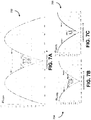
- FIG. 7 A principle of operation may be illustrated in FIG. 7 , where the inductor current ripple for a potential system and a conventional 3-level buck are shown, according to some embodiments.
- the example is illustrative and not meant to be limiting.
- FIGS. 7A, 7B and 7C provide three different plots illustrating the dependence of the normalized inductor current on the conversion ratio value for critical duty cycle avoidance modulation, as provided across various modes of operation, according to some embodiments.
- the controller is configured to operate having multiple modes (e.g., two or three modes). Three different modes are described below, but there may be more, less, and/or different modes.
- the first two modes are necessary but the third mode is optional. In another embodiment, only the first two modes are provided. In yet another embodiment, all three modes are provided.
- the critical duty cycle avoidance arbiter block may be configured for determining an operating region and may be configured to sets various values, such as d DPWM [n] and T ADPWM [n] values.
- Mode 3 may be provided not only to smooth transitions between two switching frequencies but the operation of mode 3 may also reduce a difference in the ripple amplitude between regular and skip-modulation modes. For example, an operator of the system may select a dead-band region and operate it using Mode 3.
- FIG. 7B Effect of that difference reduction can be seen in FIG. 7B , where all three modes are utilized, compared to FIG. 7C , where only Mode 1 and Mode 2 are utilized.
- Mode 3 is optional, and for applications where variable frequency is not preferable, Mode 3 can be omitted.
- Mode 2 the region where zero-ripple operating point avoidance modulation is applied, is the region where d 1 [n] and d 2 [n] values are obtained.
- d 1 [n] and d 2 [n] values are obtained.
- d 2 [n] is kept constant and d 1 [ n ] is calculated using equation (1), since, ideally, digital representation of conversion ratio is the value d PID [n].
- various hysteretic approaches may be utilized. For example, when the controller is issuing duty ratio values around 50%, it may require, in one cycle 51% and in the next cycle 50%. To avoid switching between duty ratio avoidance and conventional modes, a hysteretic controller may be utilized. The controller can switch into the duty ratio avoidance mode when the duty ratio is, for example between 49.5% and 50.5% but then use another mode when the duty ratio is between 47% and 53%. Accordingly, possible oscillations between the modes may be avoided.
- the controller may also be adapted to corrects for various variations, such as, and including, gate drive delays, level shift delays, and other real-world circuit implementation non-idealities to achieve desired duty ratios with non-overlapping switch operation.
- various variations such as, and including, gate drive delays, level shift delays, and other real-world circuit implementation non-idealities to achieve desired duty ratios with non-overlapping switch operation.
- the actual duty ratio issued by the controller where there may be problems may not be at 50% but, rather at 51% or 52%.
- a realistic converter may need to be configured to recognize that even though 52% should not be a theoretical operating point with problems, there is a problem there (but not at the point where controller is issuing a 50% control variable).
- the controller may be, in some embodiments, configured to recognize those conditions in the case where there are imperfections in the circuit.
- Such a determination may be possible with addition of various types of other circuits, for example, a switching node monitoring circuit, or by identifying a sudden increase of duty ratio control, indicating various spikes (e.g., beyond a particular threshold) and losses (e.g., beyond a particular threshold).
- a switching node monitoring circuit or by identifying a sudden increase of duty ratio control, indicating various spikes (e.g., beyond a particular threshold) and losses (e.g., beyond a particular threshold).
- FIG. 11 is an example schematic diagram of conventional digital PWM 1102 being controlled by a critical duty cycle avoidance control unit 1104, according to some embodiments.
- the digital PWM 1102 may be utilized to control the operation of converter 1106.
- FIG. 12 is an example workflow diagram illustrating various steps that may be taken in performing a method, according to some embodiments.
- the controller may be configured to perform various steps of a method, and the example steps shown are provided for illustration and are not meant to be limiting. For example, various other steps may be included and steps may be added, removed, modified, etc.
- the controller may be configured for measuring an output voltage of the multi-level converter; at 1204, comparing the measured output voltage to a reference output voltage to process an error value associated with a difference between the measured output voltage and the reference output voltage; and at 1206, determining a target duty cycle value based at least on a control feedback loop mechanism adapted to minimize the error value.
- the controller at 1210 may be configured for determining the operation of the multi-level converter to operate the multi-level converter with an averaging sequence, the averaging sequence adapted to, on average, result in, or sufficiently approximate, the one or more critical duty ratio values, but not operate at the one or more critical duty ratio values; and at 1212, controlling the operation of the multi-level converter based at least on the averaging sequence, (e.g., generating one or more pulse-width modulated signals to control the operation of the multi-level converter based on at least one of the target duty cycle and the averaging sequence).
- the controller, at 1214 may be configured for operating the converter at the target duty cycle value.
- a low-power three-level buck converter has been built, based on the schematics of FIG. 1 and FIG. 6 .
- the digital controller may be implemented with an FPGA based system, and the power stage has parameters given in Table I.
- Other Table I Summary of Design Parameters Parameter Value V IN 10 [V] Conversion Ratio 10% - 90% I OUT 10 [mA] - 3 [A] f S (nominal) 1 [MHz] L 470 [nH] C OUT 22 [ ⁇ F] C FLY 4.7 [ ⁇ F] types of technologies may also be utilized in its implementation. Performance was compared with a conventional voltage mode controller implemented with the same FPGA system. Table I is provided below: To allow comparison with the conventional prototype without damage due to voltage transients, all transistors were overrated in terms of the blocking voltage.
- the waveforms shown in FIG. 8A and FIG. 8B include: Ch1 806, 812. 5[V]/div: VDS4, Drain-source voltage of the low side M4 switch ( Fig 1 .); Ch2 808, 814. 5[V]/div: VSW, switching node voltage, Ch3 810, 816. - AC coupled 50[mV]/div: VOUT, output voltage of the converter; and Digital Probes 1-4: M1-M4 control signals (labelled as M1, M2, M3, and M4).
- FIG. 8A showing operation of the conventional controller for D ⁇ 0.5
- significant voltage spikes may be present at the switching node resulting in large voltage stress.
- FIG. 8B showing operation of the converter controlled with operating point avoidance control method, indicate that the introduced method reduced and/or effectively eliminated the voltage spikes, enabling use of lower voltage rating transistors, and thereby realizing a benefit of multi-level converter topologies.
- a possible drawback of the operating point avoidance controller may be the introduction of a larger ripple at the output voltage, as indicated at FIG. 8B .
- FIGS. 9A and 9B provide plots of sample output values related to of experimental three-level converter for gradual change of conversion ratio M from 0.25 to 0.75, according to some embodiments.
- Conventional modulation of the multi-level converters is shown in FIG. 9A and critical duty cycle avoidance modulation is applied in FIG. 9B .
- the embodiments of the devices, systems and methods described herein may be implemented in a combination of both hardware and software. These embodiments may be implemented on programmable computers, each computer including at least one processor, a data storage system (including volatile memory or non-volatile memory or other data storage elements or a combination thereof), and at least one communication interface. These embodiments may be implemented on various types of computing devices and/or technologies, such as field programmable gate arrays (FPGAs).
- FPGAs field programmable gate arrays
- Program code may be applied to input data to perform the functions described herein and to generate output information.
- the output information may be applied to one or more output devices.
- the communication interface may be a network communication interface.
- the communication interface may be a software communication interface, such as those for inter-process communication.
- there may be a combination of communication interfaces implemented as hardware, software, and combination thereof.
- connection or “coupled to” may include both direct coupling (in which two elements that are coupled to each other contact each other) and indirect coupling (in which at least one additional element is located between the two elements).
- the technical solution of embodiments may be in the form of a software and/or firmware product configured for various control steps and/or methods.
- the software and/or firmware product may be stored in a non-volatile or non-transitory storage medium, which can be a compact disk read-only memory (CD-ROM), a USB flash disk, or a removable hard disk.
- the software and/or firmware product includes a number of instructions that enable an electronic device (personal computer, server, or network device) to execute the methods provided by the embodiments.
- the embodiments described herein provide useful physical machines and particularly configured electronic hardware arrangements.
- the embodiments described herein are directed to electronic machines and methods implemented by electronic machines adapted for processing and transforming electromagnetic signals which represent various types of information.
Landscapes
- Engineering & Computer Science (AREA)
- Power Engineering (AREA)
- Dc-Dc Converters (AREA)
Claims (15)
- Système configuré pour réduire les pointes transitoires de tension entre les commutateurs dans un convertisseur CC-CC multiniveau (102), le système comprenant et étant caractérisé par :une unité configurée pour commander le fonctionnement du convertisseur CC-CC multiniveau (102) pour faire fonctionner le convertisseur CC-CC multiniveau (102) avec une séquence de moyennage, la séquence de moyennage étant adaptée pour, en moyenne, aboutir à une ou plusieurs valeurs de facteur de marche critiques, mais ne pas fonctionner à la une ou aux plusieurs valeurs de facteur de marche critiques, dans lequel la séquence de moyennage est basée au moins sur une valeur d'erreur déterminée au moins en partie par la différence entre la tension de sortie mesurée (114) et la tension de sortie de référence (110),chacune de la une ou des plusieurs valeurs de facteur de marche critiques correspondant à une valeur respective de i/(N-1), où N est un nombre de niveaux dans le convertisseur CC-CC multiniveau (102) et i est un tableau de 1 à N-2.
- Système selon la revendication 1, dans lequel le système est configuré pour effectuer une analyse de circuit automatisée afin d'identifier la une ou les plusieurs valeurs de facteur de marche critiques.
- Système selon la revendication 2, dans lequel l'analyse de circuit automatisée comprend la simulation du convertisseur CC-CC multiniveau (102) et l'approximation de la une ou des plusieurs valeurs de facteur de marche critiques sur la base d'au moins le nombre de niveaux N dans le convertisseur CC-CC multiniveau (102).
- Système selon la revendication 2, dans lequel l'analyse de circuit automatisée comprend le traitement d'informations de commande historiques stockées sur un support non transitoire lisible par machine, dans lequel la une ou les plusieurs valeurs de facteur de marche critiques est/sont identifiée(s) par des approximations basées sur au moins un des éléments suivants : réponse du circuit, caractéristiques d'entrée, caractéristiques de sortie, paramètres de commande et paramètres de fonctionnement.
- Système selon l'une quelconque des revendications 1 à 4, dans lequel l'unité est en outre configurée pour générer un ou plusieurs signaux modulés en largeur d'impulsion, et dans lequel le un ou les plusieurs signaux modulés en largeur d'impulsion comprennent la génération de signaux de commande fournis à quatre commutateurs au sein du convertisseur CC-CC multiniveau (102), les signaux de commande commandant les commutateurs pour changer d'états conformément à la séquence de moyennage.
- Système selon la revendication 5, dans lequel la séquence de moyennage assure le réglage du temps mort durant le fonctionnement du convertisseur CC-CC multiniveau (102) lorsque la valeur de cycle de service cible est égale ou approximativement égale à une ou plusieurs valeurs de facteur de marche critiques, réduisant ainsi une exigence de commande simultanée et réduisant un nombre de chemins de court-circuit.
- Système selon la revendication 5 ou 6, dans lequel le un ou les plusieurs signaux modulés en largeur d'impulsion sont configurés pour émettre des signaux de commande simultanés vers un maximum de deux commutateurs parmi les quatre commutateurs.
- Système selon l'une quelconque des revendications 1 à 7, dans lequel la séquence de moyennage est configurée pour, pendant une première moitié d'un cycle de commutation, changer une tension de nœud de commutation de 0 à VIN/2, et, pendant une seconde moitié du cycle de commutation, changer la tension de nœud de commutation de VIN/2 et VIN.
- Système selon l'une quelconque des revendications 1 à 8, dans lequel une ou plusieurs régions de bande morte sont appliquées autour de chacune de la une ou des plusieurs valeurs de facteur de marche critiques, et dans lequel lorsqu'un facteur de marche souhaité baisse dans l'une de la une ou des plusieurs régions de bande morte, la séquence de moyennage est appliquée ou utilisée pour commander le convertisseur CC-CC multiniveau (102).
- Système selon la revendication 9, dans lequel la séquence de moyennage, pendant le fonctionnement dans la une ou les plusieurs régions de bande morte, est configurée pour assurer un mode de lissage de transition, dans lequel la fréquence de commutation est progressivement réduite de fs à fs/2.
- Système selon la revendication 10, dans lequel la taille de la une ou des plusieurs régions de bande morte est déterminée sur la base d'au moins une ondulation maximale admissible.
- Système selon l'une quelconque des revendications 1 à 11, dans lequel le convertisseur CC-CC multiniveau (102) est configuré pour générer des signaux d'encadrement, où D est un rapport de cycle de service souhaité, et la une ou les plusieurs valeurs de facteur de marche critiques comprennent D = 0,5, les signaux d'encadrement commandant le fonctionnement de commutateurs correspondants du convertisseur CC-CC multiniveau (102) pour fournir la séquence de moyennage sur la base d'au moins la différence entre la tension de sortie mesurée (114) et la tension de sortie de référence (110).
- Procédé pour fournir une séquence de commutation évitant le cycle de service, qui, en moyenne, résulte en un ou plusieurs facteurs de marche souhaités ou une ou plusieurs variables de commande d'entrée générales correspondant à une ou plusieurs valeurs de facteur de marche critiques, le procédé comprenant :lorsque le ou les facteurs de marche souhaités sont égaux ou approximativement égaux à une quelconque valeur de facteur de marche critique de la une ou des plusieurs valeurs de facteur de marche critiques, contrôler le fonctionnement d'un convertisseur CC-CC multiniveau (102) pour faire fonctionner le convertisseur CC-CC multiniveau (102) conformément à une séquence de moyennage, la séquence de moyennage étant configurée pour, en moyenne, aboutir à la une ou aux plusieurs valeurs de facteur de marche critiques, mais ne pas fonctionner à la une ou aux plusieurs valeurs de facteurs de marche critiques,chacune de la une ou des plusieurs valeurs de facteurs de marche critiques correspondant à une valeur respective de i/(N-1), où N est un nombre de niveaux dans le convertisseur CC-CC multiniveau (102) et i est un tableau de 1 à N-2.
- Procédé selon la revendication 13, dans lequel le procédé est en outre configuré pour maintenir une régulation correcte de la tension de sortie, un équilibre du condensateur flottant et la symétrie de la forme d'onde du courant d'inducteur.
- Procédé selon la revendication 13 ou 14, dans lequel la séquence de commutation est configurée pour assurer une ondulation symétrique.
Applications Claiming Priority (2)
| Application Number | Priority Date | Filing Date | Title |
|---|---|---|---|
| US201562191118P | 2015-07-10 | 2015-07-10 | |
| PCT/CA2016/000191 WO2017008140A1 (fr) | 2015-07-10 | 2016-07-11 | Systèmes et procédés de réduction de tension de commutation dans des alimentations de puissance à mode commuté |
Publications (3)
| Publication Number | Publication Date |
|---|---|
| EP3320607A1 EP3320607A1 (fr) | 2018-05-16 |
| EP3320607A4 EP3320607A4 (fr) | 2019-03-06 |
| EP3320607B1 true EP3320607B1 (fr) | 2020-03-11 |
Family
ID=57756593
Family Applications (1)
| Application Number | Title | Priority Date | Filing Date |
|---|---|---|---|
| EP16823575.2A Active EP3320607B1 (fr) | 2015-07-10 | 2016-07-11 | Systèmes et procédés de réduction de tension de commutation dans des alimentations de puissance à mode commuté |
Country Status (3)
| Country | Link |
|---|---|
| US (1) | US10141832B2 (fr) |
| EP (1) | EP3320607B1 (fr) |
| WO (1) | WO2017008140A1 (fr) |
Cited By (2)
| Publication number | Priority date | Publication date | Assignee | Title |
|---|---|---|---|---|
| EP4203283A1 (fr) * | 2021-12-27 | 2023-06-28 | Infineon Technologies Austria AG | Architecture de convertisseur abaisseur-élévateur à inversion multiniveau |
| WO2024248888A1 (fr) * | 2023-05-30 | 2024-12-05 | Intel Corporation | Convertisseurs de tension utilisant un convertisseur de tension de condensateur de commutation |
Families Citing this family (13)
| Publication number | Priority date | Publication date | Assignee | Title |
|---|---|---|---|---|
| TWI742358B (zh) * | 2018-05-04 | 2021-10-11 | 德商伍爾特電子eiSos有限公司 | 功率變換器及形成其一部分的電路 |
| US10770974B2 (en) | 2019-01-16 | 2020-09-08 | Psemi Corporation | Multi-level DC-DC converter with lossless voltage balancing |
| US10720843B1 (en) | 2019-01-16 | 2020-07-21 | Psemi Corporation | Multi-level DC-DC converter with lossy voltage balancing |
| US10720842B1 (en) | 2019-01-16 | 2020-07-21 | Psemi Corporation | Multi-level DC-DC converter with boundary transition control |
| WO2020150175A1 (fr) * | 2019-01-16 | 2020-07-23 | Psemi Corporation | Convertisseur c.c.-c.c. multiniveau |
| US11303208B2 (en) | 2019-03-01 | 2022-04-12 | Apple Inc. | Cycle transitions for buck converter circuits |
| US11264896B2 (en) * | 2019-06-18 | 2022-03-01 | Kinetic Technologies | Two-phase boost converter with reduced voltage stress, and inherent current balancing |
| US11228256B2 (en) * | 2019-11-19 | 2022-01-18 | Infineon Technologies Ag | Multilevel power converter and control method |
| KR102526702B1 (ko) * | 2020-12-04 | 2023-04-28 | 한국과학기술원 | 과도 응답 향상 기술 및 플라잉 커패시터 밸런싱 기술을 포함하는 3레벨 벅 컨버터 |
| CN114175477B (zh) * | 2021-04-12 | 2025-04-08 | 深圳欣锐科技股份有限公司 | 一种基于开关电源的抖频优化方法以及装置 |
| CN113315376A (zh) * | 2021-06-21 | 2021-08-27 | 哈尔滨工业大学 | 基于电流纹波优化的可变重数dcdc变换器 |
| US20230060984A1 (en) * | 2021-09-01 | 2023-03-02 | Cirrus Logic International Semiconductor Ltd. | Adjustable power interface for maximizing converter efficiency |
| CN114785103B (zh) * | 2022-06-21 | 2022-09-02 | 绍兴圆方半导体有限公司 | 三电平电路电压纹波的控制方法、装置、电子设备 |
Family Cites Families (10)
| Publication number | Priority date | Publication date | Assignee | Title |
|---|---|---|---|---|
| US7388444B2 (en) * | 2005-10-03 | 2008-06-17 | Linear Technology Corporation | Switching regulator duty cycle control in a fixed frequency operation |
| WO2008032362A1 (fr) * | 2006-09-12 | 2008-03-20 | Mitsubishi Electric Corporation | Convertisseur cc-cc |
| WO2011016199A1 (fr) * | 2009-08-05 | 2011-02-10 | 三菱電機株式会社 | Convertisseur électrique cc/cc |
| WO2012074967A1 (fr) * | 2010-11-29 | 2012-06-07 | President And Fellows Of Harvard College | Convertisseur cc/cc à 3 niveaux entièrement intégrés, pour une mise à l'échelle de tension dynamique à l'échelle de la nanoseconde, à régulation de shunt rapide |
| EP2466740B1 (fr) * | 2010-12-14 | 2020-02-05 | Dialog Semiconductor GmbH | Circuit de régulateur à commutation hautement efficace de survolteur/dévolteur et son procédé de contrôle |
| US8441770B2 (en) * | 2011-02-18 | 2013-05-14 | ETA Semiconductor Inc | Voltage spikes control for power converters |
| US8587283B2 (en) * | 2011-04-20 | 2013-11-19 | Analog Devices, Inc. | DC-DC voltage converter system with a high-efficiency pulse-skip operational mode |
| US9906122B2 (en) * | 2012-04-03 | 2018-02-27 | Synaptics Incorporated | Methods to reduce current spikes in capacitive DC-DC converters employing gain-hopping |
| WO2014011706A1 (fr) * | 2012-07-09 | 2014-01-16 | Inertech Ip Llc | Systèmes et procédés d'alimentation sans coupure (ups) à moyenne tension multiniveaux sans transformateur |
| DE102015106773A1 (de) * | 2015-04-30 | 2016-11-03 | Dr. Ing. H.C. F. Porsche Aktiengesellschaft | Batteriesystem mit Batteriesteuerung |
-
2016
- 2016-07-11 WO PCT/CA2016/000191 patent/WO2017008140A1/fr not_active Ceased
- 2016-07-11 US US15/743,482 patent/US10141832B2/en active Active
- 2016-07-11 EP EP16823575.2A patent/EP3320607B1/fr active Active
Non-Patent Citations (1)
| Title |
|---|
| None * |
Cited By (3)
| Publication number | Priority date | Publication date | Assignee | Title |
|---|---|---|---|---|
| EP4203283A1 (fr) * | 2021-12-27 | 2023-06-28 | Infineon Technologies Austria AG | Architecture de convertisseur abaisseur-élévateur à inversion multiniveau |
| US12101030B2 (en) | 2021-12-27 | 2024-09-24 | Infineon Technologies Austria Ag | Multi-level inverting buck-boost converter architecture |
| WO2024248888A1 (fr) * | 2023-05-30 | 2024-12-05 | Intel Corporation | Convertisseurs de tension utilisant un convertisseur de tension de condensateur de commutation |
Also Published As
| Publication number | Publication date |
|---|---|
| EP3320607A1 (fr) | 2018-05-16 |
| US20180205307A1 (en) | 2018-07-19 |
| EP3320607A4 (fr) | 2019-03-06 |
| WO2017008140A1 (fr) | 2017-01-19 |
| US10141832B2 (en) | 2018-11-27 |
Similar Documents
| Publication | Publication Date | Title |
|---|---|---|
| EP3320607B1 (fr) | Systèmes et procédés de réduction de tension de commutation dans des alimentations de puissance à mode commuté | |
| US10892686B2 (en) | Hysteretic control for transformer based power converters | |
| Jang et al. | Multiphase buck converters with extended duty cycle | |
| US9086708B2 (en) | High slew rate switching regulator circuits and methods | |
| US9312772B2 (en) | Current limiting scheme for a converter | |
| US9768688B2 (en) | Asymmetric inductors in multi-phase DCDC converters | |
| JP5967871B2 (ja) | 電源装置 | |
| US11005365B2 (en) | Power converter using hysteretic boost architecture and method therefor | |
| US20120286750A1 (en) | Switching regulators with adaptive clock generators and associated methods of control | |
| US9735574B2 (en) | Switching regulator circuits and methods | |
| US20150357914A1 (en) | Method for a Current Mode Buck-Boost Converter | |
| US20160294277A1 (en) | Power converter with hysteretic buck-boost architecture and method therefor | |
| CN109997301A (zh) | 用于dc-dc电力转换器的控制方案 | |
| WO2017032269A1 (fr) | Circuit et procédé de conversion de tension, et système d'alimentation parallèle polyphasée | |
| Vukadinović et al. | Skip-duty control method for minimizing switching stress in low-power multi-level dc-dc converters | |
| JP2012253953A (ja) | 昇圧型dc−dcコンバータ | |
| Tattiwong et al. | Analysis design and experimental verification of a quadratic boost converter | |
| CN109936277A (zh) | 转换器及其驱动及控制方法 | |
| Yerra et al. | Single stage three-level interleaved buck converter with current self-balancing for improved point-of-load performance | |
| US10243460B2 (en) | Method and apparatus for dynamic voltage transition control in semi-resonant and resonant converters | |
| CN103339842B (zh) | 使用脉宽调制信号的对电子设备的滞环控制 | |
| CN114731111B (zh) | Dc/dc转换器 | |
| Zhou et al. | Voltage-mode variable frequency control for single-inductor dual-output buck converter with fast transient response | |
| Mishra | Power converter systems for consumer electronics devices | |
| Hao et al. | A wide load range high-efficiency DC-DC based on fast multi-frequency switch |
Legal Events
| Date | Code | Title | Description |
|---|---|---|---|
| STAA | Information on the status of an ep patent application or granted ep patent |
Free format text: STATUS: THE INTERNATIONAL PUBLICATION HAS BEEN MADE |
|
| PUAI | Public reference made under article 153(3) epc to a published international application that has entered the european phase |
Free format text: ORIGINAL CODE: 0009012 |
|
| STAA | Information on the status of an ep patent application or granted ep patent |
Free format text: STATUS: REQUEST FOR EXAMINATION WAS MADE |
|
| 17P | Request for examination filed |
Effective date: 20180205 |
|
| AK | Designated contracting states |
Kind code of ref document: A1 Designated state(s): AL AT BE BG CH CY CZ DE DK EE ES FI FR GB GR HR HU IE IS IT LI LT LU LV MC MK MT NL NO PL PT RO RS SE SI SK SM TR |
|
| AX | Request for extension of the european patent |
Extension state: BA ME |
|
| DAV | Request for validation of the european patent (deleted) | ||
| DAX | Request for extension of the european patent (deleted) | ||
| RAP1 | Party data changed (applicant data changed or rights of an application transferred) |
Owner name: MAXIM INTEGRATED PRODUCTS, INC. |
|
| A4 | Supplementary search report drawn up and despatched |
Effective date: 20190131 |
|
| RIC1 | Information provided on ipc code assigned before grant |
Ipc: H02M 1/00 20060101AFI20190125BHEP |
|
| GRAP | Despatch of communication of intention to grant a patent |
Free format text: ORIGINAL CODE: EPIDOSNIGR1 |
|
| STAA | Information on the status of an ep patent application or granted ep patent |
Free format text: STATUS: GRANT OF PATENT IS INTENDED |
|
| INTG | Intention to grant announced |
Effective date: 20190925 |
|
| GRAS | Grant fee paid |
Free format text: ORIGINAL CODE: EPIDOSNIGR3 |
|
| GRAA | (expected) grant |
Free format text: ORIGINAL CODE: 0009210 |
|
| STAA | Information on the status of an ep patent application or granted ep patent |
Free format text: STATUS: THE PATENT HAS BEEN GRANTED |
|
| AK | Designated contracting states |
Kind code of ref document: B1 Designated state(s): AL AT BE BG CH CY CZ DE DK EE ES FI FR GB GR HR HU IE IS IT LI LT LU LV MC MK MT NL NO PL PT RO RS SE SI SK SM TR |
|
| REG | Reference to a national code |
Ref country code: GB Ref legal event code: FG4D |
|
| REG | Reference to a national code |
Ref country code: CH Ref legal event code: EP |
|
| REG | Reference to a national code |
Ref country code: AT Ref legal event code: REF Ref document number: 1244397 Country of ref document: AT Kind code of ref document: T Effective date: 20200315 |
|
| REG | Reference to a national code |
Ref country code: IE Ref legal event code: FG4D |
|
| REG | Reference to a national code |
Ref country code: DE Ref legal event code: R096 Ref document number: 602016031723 Country of ref document: DE |
|
| PG25 | Lapsed in a contracting state [announced via postgrant information from national office to epo] |
Ref country code: FI Free format text: LAPSE BECAUSE OF FAILURE TO SUBMIT A TRANSLATION OF THE DESCRIPTION OR TO PAY THE FEE WITHIN THE PRESCRIBED TIME-LIMIT Effective date: 20200311 Ref country code: NO Free format text: LAPSE BECAUSE OF FAILURE TO SUBMIT A TRANSLATION OF THE DESCRIPTION OR TO PAY THE FEE WITHIN THE PRESCRIBED TIME-LIMIT Effective date: 20200611 Ref country code: RS Free format text: LAPSE BECAUSE OF FAILURE TO SUBMIT A TRANSLATION OF THE DESCRIPTION OR TO PAY THE FEE WITHIN THE PRESCRIBED TIME-LIMIT Effective date: 20200311 |
|
| REG | Reference to a national code |
Ref country code: NL Ref legal event code: MP Effective date: 20200311 |
|
| PG25 | Lapsed in a contracting state [announced via postgrant information from national office to epo] |
Ref country code: BG Free format text: LAPSE BECAUSE OF FAILURE TO SUBMIT A TRANSLATION OF THE DESCRIPTION OR TO PAY THE FEE WITHIN THE PRESCRIBED TIME-LIMIT Effective date: 20200611 Ref country code: LV Free format text: LAPSE BECAUSE OF FAILURE TO SUBMIT A TRANSLATION OF THE DESCRIPTION OR TO PAY THE FEE WITHIN THE PRESCRIBED TIME-LIMIT Effective date: 20200311 Ref country code: SE Free format text: LAPSE BECAUSE OF FAILURE TO SUBMIT A TRANSLATION OF THE DESCRIPTION OR TO PAY THE FEE WITHIN THE PRESCRIBED TIME-LIMIT Effective date: 20200311 Ref country code: HR Free format text: LAPSE BECAUSE OF FAILURE TO SUBMIT A TRANSLATION OF THE DESCRIPTION OR TO PAY THE FEE WITHIN THE PRESCRIBED TIME-LIMIT Effective date: 20200311 Ref country code: GR Free format text: LAPSE BECAUSE OF FAILURE TO SUBMIT A TRANSLATION OF THE DESCRIPTION OR TO PAY THE FEE WITHIN THE PRESCRIBED TIME-LIMIT Effective date: 20200612 |
|
| REG | Reference to a national code |
Ref country code: LT Ref legal event code: MG4D |
|
| PG25 | Lapsed in a contracting state [announced via postgrant information from national office to epo] |
Ref country code: NL Free format text: LAPSE BECAUSE OF FAILURE TO SUBMIT A TRANSLATION OF THE DESCRIPTION OR TO PAY THE FEE WITHIN THE PRESCRIBED TIME-LIMIT Effective date: 20200311 |
|
| PG25 | Lapsed in a contracting state [announced via postgrant information from national office to epo] |
Ref country code: PT Free format text: LAPSE BECAUSE OF FAILURE TO SUBMIT A TRANSLATION OF THE DESCRIPTION OR TO PAY THE FEE WITHIN THE PRESCRIBED TIME-LIMIT Effective date: 20200805 Ref country code: RO Free format text: LAPSE BECAUSE OF FAILURE TO SUBMIT A TRANSLATION OF THE DESCRIPTION OR TO PAY THE FEE WITHIN THE PRESCRIBED TIME-LIMIT Effective date: 20200311 Ref country code: CZ Free format text: LAPSE BECAUSE OF FAILURE TO SUBMIT A TRANSLATION OF THE DESCRIPTION OR TO PAY THE FEE WITHIN THE PRESCRIBED TIME-LIMIT Effective date: 20200311 Ref country code: LT Free format text: LAPSE BECAUSE OF FAILURE TO SUBMIT A TRANSLATION OF THE DESCRIPTION OR TO PAY THE FEE WITHIN THE PRESCRIBED TIME-LIMIT Effective date: 20200311 Ref country code: SM Free format text: LAPSE BECAUSE OF FAILURE TO SUBMIT A TRANSLATION OF THE DESCRIPTION OR TO PAY THE FEE WITHIN THE PRESCRIBED TIME-LIMIT Effective date: 20200311 Ref country code: EE Free format text: LAPSE BECAUSE OF FAILURE TO SUBMIT A TRANSLATION OF THE DESCRIPTION OR TO PAY THE FEE WITHIN THE PRESCRIBED TIME-LIMIT Effective date: 20200311 Ref country code: SK Free format text: LAPSE BECAUSE OF FAILURE TO SUBMIT A TRANSLATION OF THE DESCRIPTION OR TO PAY THE FEE WITHIN THE PRESCRIBED TIME-LIMIT Effective date: 20200311 Ref country code: IS Free format text: LAPSE BECAUSE OF FAILURE TO SUBMIT A TRANSLATION OF THE DESCRIPTION OR TO PAY THE FEE WITHIN THE PRESCRIBED TIME-LIMIT Effective date: 20200711 |
|
| REG | Reference to a national code |
Ref country code: AT Ref legal event code: MK05 Ref document number: 1244397 Country of ref document: AT Kind code of ref document: T Effective date: 20200311 |
|
| REG | Reference to a national code |
Ref country code: DE Ref legal event code: R097 Ref document number: 602016031723 Country of ref document: DE |
|
| PLBE | No opposition filed within time limit |
Free format text: ORIGINAL CODE: 0009261 |
|
| STAA | Information on the status of an ep patent application or granted ep patent |
Free format text: STATUS: NO OPPOSITION FILED WITHIN TIME LIMIT |
|
| PG25 | Lapsed in a contracting state [announced via postgrant information from national office to epo] |
Ref country code: ES Free format text: LAPSE BECAUSE OF FAILURE TO SUBMIT A TRANSLATION OF THE DESCRIPTION OR TO PAY THE FEE WITHIN THE PRESCRIBED TIME-LIMIT Effective date: 20200311 Ref country code: IT Free format text: LAPSE BECAUSE OF FAILURE TO SUBMIT A TRANSLATION OF THE DESCRIPTION OR TO PAY THE FEE WITHIN THE PRESCRIBED TIME-LIMIT Effective date: 20200311 Ref country code: AT Free format text: LAPSE BECAUSE OF FAILURE TO SUBMIT A TRANSLATION OF THE DESCRIPTION OR TO PAY THE FEE WITHIN THE PRESCRIBED TIME-LIMIT Effective date: 20200311 Ref country code: DK Free format text: LAPSE BECAUSE OF FAILURE TO SUBMIT A TRANSLATION OF THE DESCRIPTION OR TO PAY THE FEE WITHIN THE PRESCRIBED TIME-LIMIT Effective date: 20200311 |
|
| 26N | No opposition filed |
Effective date: 20201214 |
|
| PG25 | Lapsed in a contracting state [announced via postgrant information from national office to epo] |
Ref country code: PL Free format text: LAPSE BECAUSE OF FAILURE TO SUBMIT A TRANSLATION OF THE DESCRIPTION OR TO PAY THE FEE WITHIN THE PRESCRIBED TIME-LIMIT Effective date: 20200311 Ref country code: SI Free format text: LAPSE BECAUSE OF FAILURE TO SUBMIT A TRANSLATION OF THE DESCRIPTION OR TO PAY THE FEE WITHIN THE PRESCRIBED TIME-LIMIT Effective date: 20200311 Ref country code: MC Free format text: LAPSE BECAUSE OF FAILURE TO SUBMIT A TRANSLATION OF THE DESCRIPTION OR TO PAY THE FEE WITHIN THE PRESCRIBED TIME-LIMIT Effective date: 20200311 |
|
| REG | Reference to a national code |
Ref country code: CH Ref legal event code: PL |
|
| GBPC | Gb: european patent ceased through non-payment of renewal fee |
Effective date: 20200711 |
|
| REG | Reference to a national code |
Ref country code: BE Ref legal event code: MM Effective date: 20200731 |
|
| PG25 | Lapsed in a contracting state [announced via postgrant information from national office to epo] |
Ref country code: FR Free format text: LAPSE BECAUSE OF NON-PAYMENT OF DUE FEES Effective date: 20200731 Ref country code: GB Free format text: LAPSE BECAUSE OF NON-PAYMENT OF DUE FEES Effective date: 20200711 Ref country code: CH Free format text: LAPSE BECAUSE OF NON-PAYMENT OF DUE FEES Effective date: 20200731 Ref country code: LI Free format text: LAPSE BECAUSE OF NON-PAYMENT OF DUE FEES Effective date: 20200731 Ref country code: LU Free format text: LAPSE BECAUSE OF NON-PAYMENT OF DUE FEES Effective date: 20200711 |
|
| PG25 | Lapsed in a contracting state [announced via postgrant information from national office to epo] |
Ref country code: BE Free format text: LAPSE BECAUSE OF NON-PAYMENT OF DUE FEES Effective date: 20200731 |
|
| PG25 | Lapsed in a contracting state [announced via postgrant information from national office to epo] |
Ref country code: IE Free format text: LAPSE BECAUSE OF NON-PAYMENT OF DUE FEES Effective date: 20200711 |
|
| PG25 | Lapsed in a contracting state [announced via postgrant information from national office to epo] |
Ref country code: TR Free format text: LAPSE BECAUSE OF FAILURE TO SUBMIT A TRANSLATION OF THE DESCRIPTION OR TO PAY THE FEE WITHIN THE PRESCRIBED TIME-LIMIT Effective date: 20200311 Ref country code: MT Free format text: LAPSE BECAUSE OF FAILURE TO SUBMIT A TRANSLATION OF THE DESCRIPTION OR TO PAY THE FEE WITHIN THE PRESCRIBED TIME-LIMIT Effective date: 20200311 Ref country code: CY Free format text: LAPSE BECAUSE OF FAILURE TO SUBMIT A TRANSLATION OF THE DESCRIPTION OR TO PAY THE FEE WITHIN THE PRESCRIBED TIME-LIMIT Effective date: 20200311 |
|
| PG25 | Lapsed in a contracting state [announced via postgrant information from national office to epo] |
Ref country code: MK Free format text: LAPSE BECAUSE OF FAILURE TO SUBMIT A TRANSLATION OF THE DESCRIPTION OR TO PAY THE FEE WITHIN THE PRESCRIBED TIME-LIMIT Effective date: 20200311 Ref country code: AL Free format text: LAPSE BECAUSE OF FAILURE TO SUBMIT A TRANSLATION OF THE DESCRIPTION OR TO PAY THE FEE WITHIN THE PRESCRIBED TIME-LIMIT Effective date: 20200311 |
|
| PGFP | Annual fee paid to national office [announced via postgrant information from national office to epo] |
Ref country code: DE Payment date: 20250620 Year of fee payment: 10 |