EP3321957B1 - Keramik-metall-leiterplatte und halbleiterbauelement damit - Google Patents
Keramik-metall-leiterplatte und halbleiterbauelement damit Download PDFInfo
- Publication number
- EP3321957B1 EP3321957B1 EP16821132.4A EP16821132A EP3321957B1 EP 3321957 B1 EP3321957 B1 EP 3321957B1 EP 16821132 A EP16821132 A EP 16821132A EP 3321957 B1 EP3321957 B1 EP 3321957B1
- Authority
- EP
- European Patent Office
- Prior art keywords
- metal
- ceramic
- circuit board
- metal plate
- metal film
- Prior art date
- Legal status (The legal status is an assumption and is not a legal conclusion. Google has not performed a legal analysis and makes no representation as to the accuracy of the status listed.)
- Active
Links
Images


Classifications
-
- H—ELECTRICITY
- H10—SEMICONDUCTOR DEVICES; ELECTRIC SOLID-STATE DEVICES NOT OTHERWISE PROVIDED FOR
- H10W—GENERIC PACKAGES, INTERCONNECTIONS, CONNECTORS OR OTHER CONSTRUCTIONAL DETAILS OF DEVICES COVERED BY CLASS H10
- H10W40/00—Arrangements for thermal protection or thermal control
- H10W40/20—Arrangements for cooling
- H10W40/25—Arrangements for cooling characterised by their materials
- H10W40/255—Arrangements for cooling characterised by their materials having a laminate or multilayered structure, e.g. direct bond copper [DBC] ceramic substrates
-
- C—CHEMISTRY; METALLURGY
- C04—CEMENTS; CONCRETE; ARTIFICIAL STONE; CERAMICS; REFRACTORIES
- C04B—LIME, MAGNESIA; SLAG; CEMENTS; COMPOSITIONS THEREOF, e.g. MORTARS, CONCRETE OR LIKE BUILDING MATERIALS; ARTIFICIAL STONE; CERAMICS; REFRACTORIES; TREATMENT OF NATURAL STONE
- C04B37/00—Joining burned ceramic articles with other burned ceramic articles or other articles by heating
- C04B37/02—Joining burned ceramic articles with other burned ceramic articles or other articles by heating with metallic articles
- C04B37/023—Joining burned ceramic articles with other burned ceramic articles or other articles by heating with metallic articles characterised by the interlayer used
- C04B37/026—Joining burned ceramic articles with other burned ceramic articles or other articles by heating with metallic articles characterised by the interlayer used consisting of metals or metal salts
-
- H—ELECTRICITY
- H10—SEMICONDUCTOR DEVICES; ELECTRIC SOLID-STATE DEVICES NOT OTHERWISE PROVIDED FOR
- H10W—GENERIC PACKAGES, INTERCONNECTIONS, CONNECTORS OR OTHER CONSTRUCTIONAL DETAILS OF DEVICES COVERED BY CLASS H10
- H10W70/00—Package substrates; Interposers; Redistribution layers [RDL]
- H10W70/20—Conductive package substrates serving as an interconnection, e.g. metal plates
-
- H—ELECTRICITY
- H10—SEMICONDUCTOR DEVICES; ELECTRIC SOLID-STATE DEVICES NOT OTHERWISE PROVIDED FOR
- H10W—GENERIC PACKAGES, INTERCONNECTIONS, CONNECTORS OR OTHER CONSTRUCTIONAL DETAILS OF DEVICES COVERED BY CLASS H10
- H10W70/00—Package substrates; Interposers; Redistribution layers [RDL]
- H10W70/60—Insulating or insulated package substrates; Interposers; Redistribution layers
- H10W70/62—Insulating or insulated package substrates; Interposers; Redistribution layers characterised by their interconnections
- H10W70/65—Shapes or dispositions of interconnections
-
- H—ELECTRICITY
- H10—SEMICONDUCTOR DEVICES; ELECTRIC SOLID-STATE DEVICES NOT OTHERWISE PROVIDED FOR
- H10W—GENERIC PACKAGES, INTERCONNECTIONS, CONNECTORS OR OTHER CONSTRUCTIONAL DETAILS OF DEVICES COVERED BY CLASS H10
- H10W70/00—Package substrates; Interposers; Redistribution layers [RDL]
- H10W70/60—Insulating or insulated package substrates; Interposers; Redistribution layers
- H10W70/62—Insulating or insulated package substrates; Interposers; Redistribution layers characterised by their interconnections
- H10W70/66—Conductive materials thereof
-
- H—ELECTRICITY
- H10—SEMICONDUCTOR DEVICES; ELECTRIC SOLID-STATE DEVICES NOT OTHERWISE PROVIDED FOR
- H10W—GENERIC PACKAGES, INTERCONNECTIONS, CONNECTORS OR OTHER CONSTRUCTIONAL DETAILS OF DEVICES COVERED BY CLASS H10
- H10W90/00—Package configurations
-
- H—ELECTRICITY
- H10—SEMICONDUCTOR DEVICES; ELECTRIC SOLID-STATE DEVICES NOT OTHERWISE PROVIDED FOR
- H10W—GENERIC PACKAGES, INTERCONNECTIONS, CONNECTORS OR OTHER CONSTRUCTIONAL DETAILS OF DEVICES COVERED BY CLASS H10
- H10W90/00—Package configurations
- H10W90/701—Package configurations characterised by the relative positions of pads or connectors relative to package parts
-
- C—CHEMISTRY; METALLURGY
- C04—CEMENTS; CONCRETE; ARTIFICIAL STONE; CERAMICS; REFRACTORIES
- C04B—LIME, MAGNESIA; SLAG; CEMENTS; COMPOSITIONS THEREOF, e.g. MORTARS, CONCRETE OR LIKE BUILDING MATERIALS; ARTIFICIAL STONE; CERAMICS; REFRACTORIES; TREATMENT OF NATURAL STONE
- C04B2237/00—Aspects relating to ceramic laminates or to joining of ceramic articles with other articles by heating
- C04B2237/02—Aspects relating to interlayers, e.g. used to join ceramic articles with other articles by heating
- C04B2237/12—Metallic interlayers
- C04B2237/121—Metallic interlayers based on aluminium
-
- C—CHEMISTRY; METALLURGY
- C04—CEMENTS; CONCRETE; ARTIFICIAL STONE; CERAMICS; REFRACTORIES
- C04B—LIME, MAGNESIA; SLAG; CEMENTS; COMPOSITIONS THEREOF, e.g. MORTARS, CONCRETE OR LIKE BUILDING MATERIALS; ARTIFICIAL STONE; CERAMICS; REFRACTORIES; TREATMENT OF NATURAL STONE
- C04B2237/00—Aspects relating to ceramic laminates or to joining of ceramic articles with other articles by heating
- C04B2237/02—Aspects relating to interlayers, e.g. used to join ceramic articles with other articles by heating
- C04B2237/12—Metallic interlayers
- C04B2237/124—Metallic interlayers based on copper
-
- C—CHEMISTRY; METALLURGY
- C04—CEMENTS; CONCRETE; ARTIFICIAL STONE; CERAMICS; REFRACTORIES
- C04B—LIME, MAGNESIA; SLAG; CEMENTS; COMPOSITIONS THEREOF, e.g. MORTARS, CONCRETE OR LIKE BUILDING MATERIALS; ARTIFICIAL STONE; CERAMICS; REFRACTORIES; TREATMENT OF NATURAL STONE
- C04B2237/00—Aspects relating to ceramic laminates or to joining of ceramic articles with other articles by heating
- C04B2237/02—Aspects relating to interlayers, e.g. used to join ceramic articles with other articles by heating
- C04B2237/12—Metallic interlayers
- C04B2237/125—Metallic interlayers based on noble metals, e.g. silver
-
- C—CHEMISTRY; METALLURGY
- C04—CEMENTS; CONCRETE; ARTIFICIAL STONE; CERAMICS; REFRACTORIES
- C04B—LIME, MAGNESIA; SLAG; CEMENTS; COMPOSITIONS THEREOF, e.g. MORTARS, CONCRETE OR LIKE BUILDING MATERIALS; ARTIFICIAL STONE; CERAMICS; REFRACTORIES; TREATMENT OF NATURAL STONE
- C04B2237/00—Aspects relating to ceramic laminates or to joining of ceramic articles with other articles by heating
- C04B2237/30—Composition of layers of ceramic laminates or of ceramic or metallic articles to be joined by heating, e.g. Si substrates
- C04B2237/32—Ceramic
- C04B2237/34—Oxidic
- C04B2237/343—Alumina or aluminates
-
- C—CHEMISTRY; METALLURGY
- C04—CEMENTS; CONCRETE; ARTIFICIAL STONE; CERAMICS; REFRACTORIES
- C04B—LIME, MAGNESIA; SLAG; CEMENTS; COMPOSITIONS THEREOF, e.g. MORTARS, CONCRETE OR LIKE BUILDING MATERIALS; ARTIFICIAL STONE; CERAMICS; REFRACTORIES; TREATMENT OF NATURAL STONE
- C04B2237/00—Aspects relating to ceramic laminates or to joining of ceramic articles with other articles by heating
- C04B2237/30—Composition of layers of ceramic laminates or of ceramic or metallic articles to be joined by heating, e.g. Si substrates
- C04B2237/32—Ceramic
- C04B2237/36—Non-oxidic
- C04B2237/366—Aluminium nitride
-
- C—CHEMISTRY; METALLURGY
- C04—CEMENTS; CONCRETE; ARTIFICIAL STONE; CERAMICS; REFRACTORIES
- C04B—LIME, MAGNESIA; SLAG; CEMENTS; COMPOSITIONS THEREOF, e.g. MORTARS, CONCRETE OR LIKE BUILDING MATERIALS; ARTIFICIAL STONE; CERAMICS; REFRACTORIES; TREATMENT OF NATURAL STONE
- C04B2237/00—Aspects relating to ceramic laminates or to joining of ceramic articles with other articles by heating
- C04B2237/30—Composition of layers of ceramic laminates or of ceramic or metallic articles to be joined by heating, e.g. Si substrates
- C04B2237/32—Ceramic
- C04B2237/36—Non-oxidic
- C04B2237/368—Silicon nitride
-
- C—CHEMISTRY; METALLURGY
- C04—CEMENTS; CONCRETE; ARTIFICIAL STONE; CERAMICS; REFRACTORIES
- C04B—LIME, MAGNESIA; SLAG; CEMENTS; COMPOSITIONS THEREOF, e.g. MORTARS, CONCRETE OR LIKE BUILDING MATERIALS; ARTIFICIAL STONE; CERAMICS; REFRACTORIES; TREATMENT OF NATURAL STONE
- C04B2237/00—Aspects relating to ceramic laminates or to joining of ceramic articles with other articles by heating
- C04B2237/30—Composition of layers of ceramic laminates or of ceramic or metallic articles to be joined by heating, e.g. Si substrates
- C04B2237/40—Metallic
- C04B2237/402—Aluminium
-
- C—CHEMISTRY; METALLURGY
- C04—CEMENTS; CONCRETE; ARTIFICIAL STONE; CERAMICS; REFRACTORIES
- C04B—LIME, MAGNESIA; SLAG; CEMENTS; COMPOSITIONS THEREOF, e.g. MORTARS, CONCRETE OR LIKE BUILDING MATERIALS; ARTIFICIAL STONE; CERAMICS; REFRACTORIES; TREATMENT OF NATURAL STONE
- C04B2237/00—Aspects relating to ceramic laminates or to joining of ceramic articles with other articles by heating
- C04B2237/30—Composition of layers of ceramic laminates or of ceramic or metallic articles to be joined by heating, e.g. Si substrates
- C04B2237/40—Metallic
- C04B2237/407—Copper
-
- C—CHEMISTRY; METALLURGY
- C04—CEMENTS; CONCRETE; ARTIFICIAL STONE; CERAMICS; REFRACTORIES
- C04B—LIME, MAGNESIA; SLAG; CEMENTS; COMPOSITIONS THEREOF, e.g. MORTARS, CONCRETE OR LIKE BUILDING MATERIALS; ARTIFICIAL STONE; CERAMICS; REFRACTORIES; TREATMENT OF NATURAL STONE
- C04B2237/00—Aspects relating to ceramic laminates or to joining of ceramic articles with other articles by heating
- C04B2237/50—Processing aspects relating to ceramic laminates or to the joining of ceramic articles with other articles by heating
- C04B2237/70—Forming laminates or joined articles comprising layers of a specific, unusual thickness
- C04B2237/704—Forming laminates or joined articles comprising layers of a specific, unusual thickness of one or more of the ceramic layers or articles
-
- C—CHEMISTRY; METALLURGY
- C04—CEMENTS; CONCRETE; ARTIFICIAL STONE; CERAMICS; REFRACTORIES
- C04B—LIME, MAGNESIA; SLAG; CEMENTS; COMPOSITIONS THEREOF, e.g. MORTARS, CONCRETE OR LIKE BUILDING MATERIALS; ARTIFICIAL STONE; CERAMICS; REFRACTORIES; TREATMENT OF NATURAL STONE
- C04B2237/00—Aspects relating to ceramic laminates or to joining of ceramic articles with other articles by heating
- C04B2237/50—Processing aspects relating to ceramic laminates or to the joining of ceramic articles with other articles by heating
- C04B2237/70—Forming laminates or joined articles comprising layers of a specific, unusual thickness
- C04B2237/706—Forming laminates or joined articles comprising layers of a specific, unusual thickness of one or more of the metallic layers or articles
-
- C—CHEMISTRY; METALLURGY
- C04—CEMENTS; CONCRETE; ARTIFICIAL STONE; CERAMICS; REFRACTORIES
- C04B—LIME, MAGNESIA; SLAG; CEMENTS; COMPOSITIONS THEREOF, e.g. MORTARS, CONCRETE OR LIKE BUILDING MATERIALS; ARTIFICIAL STONE; CERAMICS; REFRACTORIES; TREATMENT OF NATURAL STONE
- C04B2237/00—Aspects relating to ceramic laminates or to joining of ceramic articles with other articles by heating
- C04B2237/50—Processing aspects relating to ceramic laminates or to the joining of ceramic articles with other articles by heating
- C04B2237/70—Forming laminates or joined articles comprising layers of a specific, unusual thickness
- C04B2237/708—Forming laminates or joined articles comprising layers of a specific, unusual thickness of one or more of the interlayers
-
- C—CHEMISTRY; METALLURGY
- C04—CEMENTS; CONCRETE; ARTIFICIAL STONE; CERAMICS; REFRACTORIES
- C04B—LIME, MAGNESIA; SLAG; CEMENTS; COMPOSITIONS THEREOF, e.g. MORTARS, CONCRETE OR LIKE BUILDING MATERIALS; ARTIFICIAL STONE; CERAMICS; REFRACTORIES; TREATMENT OF NATURAL STONE
- C04B2237/00—Aspects relating to ceramic laminates or to joining of ceramic articles with other articles by heating
- C04B2237/50—Processing aspects relating to ceramic laminates or to the joining of ceramic articles with other articles by heating
- C04B2237/72—Forming laminates or joined articles comprising at least two interlayers directly next to each other
-
- C—CHEMISTRY; METALLURGY
- C04—CEMENTS; CONCRETE; ARTIFICIAL STONE; CERAMICS; REFRACTORIES
- C04B—LIME, MAGNESIA; SLAG; CEMENTS; COMPOSITIONS THEREOF, e.g. MORTARS, CONCRETE OR LIKE BUILDING MATERIALS; ARTIFICIAL STONE; CERAMICS; REFRACTORIES; TREATMENT OF NATURAL STONE
- C04B2237/00—Aspects relating to ceramic laminates or to joining of ceramic articles with other articles by heating
- C04B2237/50—Processing aspects relating to ceramic laminates or to the joining of ceramic articles with other articles by heating
- C04B2237/86—Joining of two substrates at their largest surfaces, one surface being complete joined and covered, the other surface not, e.g. a small plate joined at it's largest surface on top of a larger plate
-
- C—CHEMISTRY; METALLURGY
- C04—CEMENTS; CONCRETE; ARTIFICIAL STONE; CERAMICS; REFRACTORIES
- C04B—LIME, MAGNESIA; SLAG; CEMENTS; COMPOSITIONS THEREOF, e.g. MORTARS, CONCRETE OR LIKE BUILDING MATERIALS; ARTIFICIAL STONE; CERAMICS; REFRACTORIES; TREATMENT OF NATURAL STONE
- C04B2237/00—Aspects relating to ceramic laminates or to joining of ceramic articles with other articles by heating
- C04B2237/50—Processing aspects relating to ceramic laminates or to the joining of ceramic articles with other articles by heating
- C04B2237/88—Joining of two substrates, where a substantial part of the joining material is present outside of the joint, leading to an outside joining of the joint
-
- H—ELECTRICITY
- H10—SEMICONDUCTOR DEVICES; ELECTRIC SOLID-STATE DEVICES NOT OTHERWISE PROVIDED FOR
- H10W—GENERIC PACKAGES, INTERCONNECTIONS, CONNECTORS OR OTHER CONSTRUCTIONAL DETAILS OF DEVICES COVERED BY CLASS H10
- H10W40/00—Arrangements for thermal protection or thermal control
- H10W40/01—Manufacture or treatment
- H10W40/03—Manufacture or treatment of arrangements for cooling
- H10W40/037—Assembling together parts thereof
-
- H—ELECTRICITY
- H10—SEMICONDUCTOR DEVICES; ELECTRIC SOLID-STATE DEVICES NOT OTHERWISE PROVIDED FOR
- H10W—GENERIC PACKAGES, INTERCONNECTIONS, CONNECTORS OR OTHER CONSTRUCTIONAL DETAILS OF DEVICES COVERED BY CLASS H10
- H10W40/00—Arrangements for thermal protection or thermal control
- H10W40/20—Arrangements for cooling
- H10W40/22—Arrangements for cooling characterised by their shape, e.g. having conical or cylindrical projections
-
- H—ELECTRICITY
- H10—SEMICONDUCTOR DEVICES; ELECTRIC SOLID-STATE DEVICES NOT OTHERWISE PROVIDED FOR
- H10W—GENERIC PACKAGES, INTERCONNECTIONS, CONNECTORS OR OTHER CONSTRUCTIONAL DETAILS OF DEVICES COVERED BY CLASS H10
- H10W70/00—Package substrates; Interposers; Redistribution layers [RDL]
- H10W70/60—Insulating or insulated package substrates; Interposers; Redistribution layers
- H10W70/67—Insulating or insulated package substrates; Interposers; Redistribution layers characterised by their insulating layers or insulating parts
- H10W70/69—Insulating materials thereof
- H10W70/692—Ceramics or glasses
-
- H—ELECTRICITY
- H10—SEMICONDUCTOR DEVICES; ELECTRIC SOLID-STATE DEVICES NOT OTHERWISE PROVIDED FOR
- H10W—GENERIC PACKAGES, INTERCONNECTIONS, CONNECTORS OR OTHER CONSTRUCTIONAL DETAILS OF DEVICES COVERED BY CLASS H10
- H10W72/00—Interconnections or connectors in packages
- H10W72/30—Die-attach connectors
- H10W72/351—Materials of die-attach connectors
- H10W72/352—Materials of die-attach connectors comprising metals or metalloids, e.g. solders
-
- H—ELECTRICITY
- H10—SEMICONDUCTOR DEVICES; ELECTRIC SOLID-STATE DEVICES NOT OTHERWISE PROVIDED FOR
- H10W—GENERIC PACKAGES, INTERCONNECTIONS, CONNECTORS OR OTHER CONSTRUCTIONAL DETAILS OF DEVICES COVERED BY CLASS H10
- H10W72/00—Interconnections or connectors in packages
- H10W72/851—Dispositions of multiple connectors or interconnections
- H10W72/874—On different surfaces
- H10W72/884—Die-attach connectors and bond wires
-
- H—ELECTRICITY
- H10—SEMICONDUCTOR DEVICES; ELECTRIC SOLID-STATE DEVICES NOT OTHERWISE PROVIDED FOR
- H10W—GENERIC PACKAGES, INTERCONNECTIONS, CONNECTORS OR OTHER CONSTRUCTIONAL DETAILS OF DEVICES COVERED BY CLASS H10
- H10W90/00—Package configurations
- H10W90/701—Package configurations characterised by the relative positions of pads or connectors relative to package parts
- H10W90/731—Package configurations characterised by the relative positions of pads or connectors relative to package parts of die-attach connectors
- H10W90/734—Package configurations characterised by the relative positions of pads or connectors relative to package parts of die-attach connectors between a chip and a stacked insulating package substrate, interposer or RDL
-
- H—ELECTRICITY
- H10—SEMICONDUCTOR DEVICES; ELECTRIC SOLID-STATE DEVICES NOT OTHERWISE PROVIDED FOR
- H10W—GENERIC PACKAGES, INTERCONNECTIONS, CONNECTORS OR OTHER CONSTRUCTIONAL DETAILS OF DEVICES COVERED BY CLASS H10
- H10W90/00—Package configurations
- H10W90/701—Package configurations characterised by the relative positions of pads or connectors relative to package parts
- H10W90/731—Package configurations characterised by the relative positions of pads or connectors relative to package parts of die-attach connectors
- H10W90/736—Package configurations characterised by the relative positions of pads or connectors relative to package parts of die-attach connectors between a chip and a stacked lead frame, conducting package substrate or heat sink
-
- H—ELECTRICITY
- H10—SEMICONDUCTOR DEVICES; ELECTRIC SOLID-STATE DEVICES NOT OTHERWISE PROVIDED FOR
- H10W—GENERIC PACKAGES, INTERCONNECTIONS, CONNECTORS OR OTHER CONSTRUCTIONAL DETAILS OF DEVICES COVERED BY CLASS H10
- H10W90/00—Package configurations
- H10W90/701—Package configurations characterised by the relative positions of pads or connectors relative to package parts
- H10W90/751—Package configurations characterised by the relative positions of pads or connectors relative to package parts of bond wires
- H10W90/754—Package configurations characterised by the relative positions of pads or connectors relative to package parts of bond wires between a chip and a stacked insulating package substrate, interposer or RDL
Definitions
- the invention relates to a ceramic metal circuit board and a semiconductor device using the same.
- a ceramic metal circuit board is formed by bonding a metal plate onto a ceramic substrate such as an aluminum oxide (Al 2 O 3 ) substrate, an aluminum nitride (A1N) substrate, and a silicon nitride (Si 3 N 4 ) substrate.
- a metal plate a copper (Cu) plate and/or an aluminum (Al) plate is used.
- a bonding method of using a brazing material is widely used for bonding the metal plate onto the ceramic substrate.
- a brazing material containing at least one of active metal such as Ti, Zr, Hf, and Si is used.
- active metal such as Ti, Zr, Hf, and Si
- a brazing material containing Ag and Cu as main components is exemplified.
- a brazing material using Si as an active metal a brazing material containing Al as a main component can be exemplified.
- Patent Document 2 discloses a method that is capable of producing a metal/ceramic bonding substrate at low costs by forming a desired fillet on the peripheral portion of a metal circuit by a small number of steps.
- an active metal containing brazing filler metal is applied on a ceramic substrate to bond a metal member thereto, a resist is applied on a predetermined portion of a surface of the metal member to etch unnecessary portions, and then the resist is removed. Thereafter, unnecessary part of a metal layer, which is formed of a metal other than an active metal of the active metal containing brazing filler metal, is etched with a chemical to be removed.
- an active metal layer which is formed of the active metal and a compound thereof, is selectively etched with a chemical, which inhibits the metal member and the metal layer from being etched and which selectively etch the active metal layer, to form a metal circuit on the ceramic substrate.
- This metal circuit is chemically polished to form a fillet on the peripheral portion of the metal circuit.
- Patent Documents 3 and 4 in each case disclose a metal/ceramic circuit board that is capable of eliminating discrepancy during mounting of parts to improve the reliability of mounting of the parts.
- the metal/ceramic circuit board has a ceramic substrate and a metal circuit plate (a copper plate) bonded to the ceramic substrate, wherein the metal circuit plate has a thickness of 0.1 mm to 0.5 mm and has a skirt spreading length (a dimensional difference between the bottom and top portion of the peripheral edge portion of the metal circuit plate) of less than 50 ⁇ m.
- the metal circuit plate is treated by nickel plating, nickel alloy plating, gold plating or preservation.
- Patent Document 5 discloses a method that is capable of producing a metal/ceramic bonding member while improving the adhesion of plating and productivity, without using any organic solvent-soluble resists and without carrying out any heat treatments.
- an electroless nickel alloy plating layer is formed on a predetermined portion of the surface of an aluminum plate which is bonded to at least one side of a ceramic substrate and which is formed so as to have a predetermined circuit pattern
- an alkali peeling type resist having a predetermined shape is applied on the surface of the aluminum plate before forming the electroless nickel alloy plating layer, and then, a portion of the surface of the aluminum plate, on which the resist is not applied, is activated with an acidic zinc immersion solution containing a fluoride or silicofluoride. Then, after the electroless nickel alloy plating layer is formed, the resist is removed with an alkali.
- Solder is used for mounting a semiconductor element on a metal plate.
- lead-free solder in view of toxicity of lead.
- JIS-Z-3282 Japanese Industrial Standard
- lead-free solders such as Sn-Ag type, Sn-Cu type, and Sn-Zn type are used.
- Lead-free solder is satisfactory in terms of wettability with a Ni plating layer, further improvement has not been expected. Thus, there is a limit in further improving reliability of bonding with a semiconductor element.
- a metal plate i.e., rear metal plate
- a heat dissipation member heat radiating member
- Metal such as copper and aluminum is mainly used for a constituent material of the heat dissipation member.
- Grease is used for bonding the rear metal plate to the heat dissipation member.
- an object of the present invention is to provide a ceramic metal circuit board having improved bondability of the front metal plate and the rear metal plate even when the parts to be connected and the like are different between the front and rear metal plates.
- the invention is defined by the claims.
- the invention thus relates to a ceramic metal circuit board as defined in claim 1.
- the ceramic metal circuit board includes:
- the invention in a second aspect, relates to a semiconductor device as defined in claim 12.
- the semiconductor device is configured by mounting a semiconductor element on the ceramic metal circuit board according to the first aspect.
- a metal film is provided on a surface of one metal plate and at least a part of another metal plate is not provided with the metal film.
- Fig. 1 illustrates a configuration of a ceramic metal circuit board.
- the reference sign 1 denotes a ceramic metal circuit board
- the numeral 2 denotes a ceramic substrate
- the numeral 3 denotes a metal plate (front metal plate)
- the numeral 4 denotes a metal plate (rear metal plate)
- the numeral 5 denotes a bonding layer (front-side bonding layer)
- the numeral 6 denotes a bonding layer (rear-side bonding layer)
- the numeral 7 denotes a metal film (rear-side metal film).
- protruding portions 5a and 6a are formed as the portions of the respective bonding layers 5 and 6 such that the bonding layers 5 and 6 protrude from the side surfaces of the respective metal plates 3 and 4.
- An aluminum nitride substrate is a substrate containing aluminum nitride (A1N) as a main component.
- A1N aluminum nitride
- an aluminum nitride substrate generally has a high thermal conductivity, its three-point bending strength is as low as 550 MPa or less. Further, the average three-point bending strength of an aluminum nitride substrate is 200 to 400 MPa. Thus, it is preferable that thickness of an aluminum nitride substrate is as thick as 0.50 mm or more.
- the metal plates are preferably made of one material selected from copper, a copper alloy, aluminum, and an aluminum alloy. Copper and aluminum are materials having high thermal conductivity and high electrical conductivity.
- the thickness of each metal plate is preferably set to 0.20 mm or more. By increasing the thickness of each metal plate, heat dissipation property can be improved. Although the upper limit of the thickness of each metal plate is not particularly limited, the thickness is preferably 5.00 mm or less in view of easiness of processing into a predetermined circuit pattern shape.
- a metal film is provided on a surface of one metal plate provided on one surface of the ceramic substrate and (b) at least a part of another metal plate provided on another surface of the ceramic substrate is not provided with the metal film.
- the rear-side metal plate is preferably provided with a metal film which has a linear expansion coefficient smaller than the linear expansion coefficient of the rear-side metal plate.
- a metal film having a smaller linear expansion coefficient than that of a metal plate it is possible to make the rear-side metal plate slightly convex.
- copper (Cu) is 16.8 ppm/K
- aluminum (Al) is 23 ppm/K
- nickel (Ni) is 12.8 ppm/K
- gold (Au) is 14.3 ppm/K.
- the surface of the rear-side copper plate tends to become convex as the linear expansion coefficient of Ni is smaller than that of the front-side copper plate which is not provided with the Ni film.
- This structure enables such a mounting so that grease uniformly expands outward, when a mounting structure in which a stress directly applied to the ceramic substrate is taken as shown in FIG. 7 to be described below.
- This structure can reduce formation of bubbles in the grease layer. From this point as well, it is preferable to provide a metal film mainly composed of Ni or Au on a copper plate or an aluminum plate. This is a synergistic effect utilizing the satisfactory wettability between the metal film and the grease and the difference in linear expansion coefficient between the metal plate and the metal film.
- Ni and Au have high corrosion resistance, rusting of each metal plate can be prevented.
- the rust of each metal plate is mainly composed of oxide. Since these rusts act as thermal resistors, it is preferable to prevent generation of these rusts.
- the average thickness of the metal film is 10 ⁇ m or less. Even when the metal film is formed to be excessively thick, further effects cannot be obtained. When plural metal plates are bonded as shown in FIG. 4 , there is a possibility that adjacent metal plates are electrically connected to each other. Thus, the average thickness of the metal film is 10 ⁇ m or less, preferably 5 ⁇ m or less.
- Measurement of the film thickness of the metal film is performed by measuring thickness values at arbitrary three positions and setting the average of the three measured thickness values as the average film thickness.
- the metal film is provided on the side surface of the metal plate as described later, the thickness in the side direction is measured.
- the metal film formation method is not limited to particular methods such as a plating method and a sputtering method.
- the metal plate provided with the metal film has a recrystallized structure.
- Copper (or copper alloy) or aluminum (or aluminum alloy) is used for the constituent material of the metal plate as described above.
- the bonding temperature for bonding the ceramic substrate and the metal plate is as high as 600 to 900°C.
- the recrystallization temperature of copper is approximately 220°C, and the recrystallization temperature of aluminum is approximately 200°C. For this reason, a copper plate and an aluminum plate have a recrystallized structure after being bonded to the ceramic substrate.
- the secondary recrystallized grains have an average grain size of 200 to 1000 ⁇ m.
- the maximum height surface roughness Rz of the metal plate surface becomes 2 ⁇ m or more, further 4 ⁇ m or more.
- the maximum height surface roughness Rz can be reduced to be 1.5 ⁇ m or less, further 0.8 ⁇ m or less. By reducing the maximum height surface roughness Rz, it is possible to improve the close-contacting property with the heat dissipation member.
- the rear-side metal plate 4 is mounted on a heat dissipation member such as a heat dissipation fin 14.
- a heat dissipation member such as a heat dissipation fin 14.
- the metal plates 3 and 4 are copper plates (including copper alloy plates) or aluminum plates (including aluminum alloy plates) and the average crystal grain size reaches 200 ⁇ m or more, it may be determined that secondary recrystallization occurs on the metal plates 3 and 4.
- a portion where no metal film is provided is formed on the surface of the front metal plate 3.
- the portion where the metal film is not provided is used as a portion where a semiconductor element or a metal terminal is mounted as described below. In other words, since it is enough that a metal film is not provided at the portion where the semiconductor element 11 or the metal terminal 9 is mounted, while a metal film may be provided or may not be provided at a portion which is not used for mounting.
- the portions where the metal film 7 is provided are different between the front metal plate 3 and the rear metal plate 4, the front and rear surfaces can be distinguished from the appearance, and thus the handling property of the ceramic metal circuit board can be improved.
- the protruding portions 5a and 6a protruding from the respective side surfaces of the metal plates 3 and 4 are formed as end portions of the respective bonding layers 5 and 6.
- the protruding portions 5a and 6a of the bonding layers 5 and 6 are portions which protrude from the respective side surfaces of the metal plates 5 and 6. The presence of the protruding portions 5a and 6a can relieve the stress caused at the bonding end portion between the ceramic substrate 2 and the metal plates 3 and 4. Thus, it becomes possible to improve the heat-cycle resistance characteristics.
- the length of each of the protruding portions 5a and 6a is preferably set to within a range of 0.005 to 0.3 mm (i.e., 5 to 300 ⁇ m).
- 0.005 mm i.e., 5 to 300 ⁇ m
- the effect of providing the protruding portions 5a and 6a cannot be sufficiently obtained.
- the length of each of protruding portions 5a and 6a exceeds 0.3 mm (i.e., 300 ⁇ m), it also suffers from circuit design restrictions such as increasing the gap between adjacent metal plates, in addition to that further effects cannot be obtained.
- each of the protruding portions 5a and 6a is preferably set within the range of 0.005 to 0.3 mm, more preferably within the range of 0.01 to 0.1 mm. Additionally, the protruding portions 5a and 6a may be shaped so as to climb up to the respective side surfaces of the metal plates 3 and 4.
- the protruding portions of the respective bonding layers 5 and 6 by covering the protruding portions of the respective bonding layers 5 and 6 with the metal films, it is possible to improve the heat cycle resistance characteristics (TCT characteristics). Performance of semiconductor devices has been advanced and improved. As a result, the junction temperature rises. In a SiC element, the junction temperature reaches 150°C or higher. When a semiconductor device is exposed to a high-temperature environment for a long time, there is a possibility that a protruding portion of each bonding layer is disadvantageously deformed. However, by covering the respective protruding portions 5a and 6a with the metal films, deformation of the protruding portions 5a and 6a can be suppressed.
- the bonding layer containing a soft metal such as Ag, Cu, and Al there is a high possibility that the protruding portions are deformed.
- a soft metal such as Ag, Cu, and Al
- the respective protruding portions 5a and 6a are covered with the metal films, such deformation of the protruding portions 5a and 6a can be effectively suppressed.
- the TCT characteristics of the circuit board can be drastically improved.
- FIG. 3 illustrates a configuration of a ceramic metal circuit board according to one embodiment in which a metal terminal 9 is bonded.
- the reference sign 1 denotes a ceramic metal circuit board
- the sign 2 denotes a ceramic substrate
- the sign 3 denotes a metal plate (front metal plate)
- the sign 4 denotes a metal plate (rear metal plate)
- the sign 5 denotes a bonding layer (front-side bonding layer)
- the sign 6 denotes a bonding layer (rear-side bonding layer)
- the sign 7 denotes a metal film (rear-side metal film)
- the sign 8 denotes a metal film (front-side-surface side metal film)
- the sign 9 denotes a metal terminal.
- the metal terminal 9 is preferably made of one selected from copper, a copper alloy, aluminum, an aluminum alloy, iron, and an iron alloy.
- the metal terminal 9 is connected to the surface of the front metal plate 3.
- methods such as a soldering method, an ultrasonic bonding method, and a pressure bonding method can be applied.
- FIG. 4 illustrates a configuration of a ceramic metal circuit board in which the plural front metal plates are bonded.
- the reference sign 1 denotes a ceramic metal circuit board
- the sign 2 denotes a ceramic substrate
- the sign 3-1 denotes a first metal plate (front metal plate)
- the sign 3-2 denotes a second metal plate (front metal plate)
- the sign 4 denotes a metal plate (rear metal plate)
- the sign 5 denotes a bonding layer (front-side bonding layer)
- the sign 6 denotes a bonding layer (rear-side bonding layer)
- the sign 7 denotes a metal film (rear-side metal film)
- the sign 8 denotes a metal film (front-side-surface side metal film).
- FIG. 4 illustrates a configuration in which two front metal plates 3-1 and 3-2 are disposed. The number of the front metal plates (3-1, 3-2) of the ceramic metal circuit board 1 is
- the above-described ceramic metal circuit board 1 is effective for a semiconductor device in which a semiconductor element is mounted.
- the semiconductor element is mounted through a solder layer at such a portion that a metal film is not provided on the surface of the metal plate.
- the solder layer is made of lead-free solder.
- FIG. 5 illustrates a configuration of a semiconductor device according to another embodiment.
- the reference sign 1 denotes a ceramic metal circuit board
- the sign 2 denotes a ceramic substrate
- the sign 3 denotes a metal plate (front metal plate)
- the sign 4 denotes a metal plate (rear metal plate)
- the sign 5 denotes a bonding layer (front-side bonding layer)
- the sign 6 denotes a bonding layer (rear-side bonding layer)
- the sign 7 denotes a metal film (rear-side metal film)
- the sign 8 denotes a metal film (front-side-surface side metal film)
- the sign 10 denotes a semiconductor device
- the sign 11 denotes a semiconductor element
- the sign 12 denotes a solder layer
- the sign 14 denotes a heat dissipation fin.
- the semiconductor element 11 is mounted on the front metal plate 3 through the solder layer 12.
- the solder layer 12 is provided on the portion of the front metal plate 3 where the metal film is not provided. Further, it is preferable that the solder layer 12 is made of lead-free solder.
- FIG. 6 illustrates a configuration of a semiconductor device according to another embodiment.
- the reference sign 1 denotes a ceramic metal circuit board
- the sign 2 denotes a ceramic substrate
- the sign 3 denotes a metal plate (front metal plate)
- the sign 4 denotes a metal plate (rear metal plate)
- the sign 5 denotes a bonding layer (front-side bonding layer)
- the sign 6 denotes a bonding layer (rear-side bonding layer)
- the sign 7 denotes a metal film (rear-side metal film)
- the sign 8 denotes a metal film (front-side-surface side metal film)
- the sign 9 denotes a metal terminal
- the sign 10 denotes a semiconductor device
- the sign 11 denotes a semiconductor element
- the sign 12 denotes a solder layer
- the sign 14 denotes a heat dissipation fin
- the sign 15 denotes a screw.
- FIG. 6 illustrates the semiconductor device 10 in which the respective semiconductor elements 11 are mounted on the two metal plates 3 through the respective solder layers 12.
- the metal terminal 9 is used for electrical conduction to the semiconductor element 11 and the heat dissipation fin 14 is fixed with the screws 15.
- a method of making the electrical conduction to the semiconductor element 11 is not limited to the method of using the metal terminal 9 as shown in FIG. 6 , and wire bonding method may be also used instead.
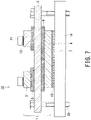
- FIG. 7 illustrates still another configuration of a semiconductor device.
- the reference sign 1 denotes a ceramic metal circuit board
- the sign 2 denotes a ceramic substrate
- the sign 3 denotes a metal plate (front metal plate)
- the sign 4 denotes a metal plate (rear metal plate)
- the sign 5 denotes a bonding layer (front-side bonding layer)
- the sign 6 denotes a bonding layer (rear-side bonding layer)
- the sign 7 denotes a metal film (rear-side metal film)
- the sign 10 denotes a semiconductor device
- the sign 11 denotes a semiconductor element
- the sign 12 denotes a solder layer
- the sign 13 denotes a grease layer
- the sign 14 denotes a heat dissipation fin
- the sign 15 denotes a screw.
- the above-described lead-free solder is exemplified in JIS-Z-3282 (2006).
- the lead-free solder contains Sn (tin) as a main component.
- the term "main component" as used herein means a component which is included most in the solder components by mass%.
- additives are adjusted to select characteristics such as high temperature type, medium high temperature type, and medium temperature type.
- the lead-free solder contains Ag in contents of 5% or less by mass, the lead-free solder also contains much Sn which is hard to react with a sulfur component and thus no reactant (AgS) is produced.
- the semiconductor device is not limited to a type in which lead-free solder is used for bonding, and various bonding materials may be also used. Lead-based solders are also included in these various bonding materials to be used for the semiconductor device.
- the rear metal plate 4 is bonded to the heat dissipation fin 14 through the solder layer 12 or the grease layer 13.
- various heat dissipating members such as a heat dissipation plate (heat sink) and a casing can be also used instead of the heat dissipation fin 14.
- a solder layer and an adhesive layer may be also used.
- a screwing structure or a pressure-contacting structure is used.
- constituent materials of the heat dissipation member include copper, a copper alloy, aluminum, an aluminum alloy, iron, an iron alloy, and ceramics. Further, as necessary, the semiconductor device 10 is resin-molded.
- a power cycle characteristic test is a durability test in which a switching operation is repeatedly performed under the state where temperature of a semiconductor device is relatively stable. This is a test to reproduce a failure mode performed while ON/OFF of the semiconductor element is repeated.
- the heat dissipation property is unsatisfactory, the heat of the semiconductor element does not sufficiently escape and thus a bonding failure is likely to occur.
- the semiconductor element is a power element, it is sometimes called a disconnection energization test.
- the method of manufacturing the ceramic metal circuit board is not particularly limited, but the following procedure can be adopted as a method for efficiently producing it.
- a ceramic substrate is prepared.
- any one of a silicon nitride substrate, an aluminum nitride substrate, and an aluminum oxide substrate is preferable.
- the silicon nitride substrate, the aluminum nitride substrate, and the aluminum oxide substrate are preferably the substrates as described hereinbefore.
- the thickness of the substrate is preferably set within a range of 0.1 to 1.0 mm. Further, the substrate thickness is selected depending on required strength and thermal conductivity of the substrate.
- a metal plate is prepared. It is preferable that the metal plate is one selected from copper, a copper alloy, aluminum, and an aluminum alloy.
- the thickness of the metal plate is preferably set within a range of 0.2 to 5.0 mm.
- an active metal brazing material is prepared. It is preferable that the active metal is one selected from Ti, Zr, Hf, and Si.
- the metal plate is a copper plate or a copper alloy plate
- an active metal brazing material which contains Ag and Cu and further contains one of active metals selected from Ti, Zr, and Hf.
- active metals selected from Ti, Zr, and Hf.
- one or both of Sn and In are contained in the active metal brazing material.
- the metal plate is an aluminum plate or an aluminum alloy plate
- an active metal brazing material which contains Si and Al.
- one or more elements selected from Mg, Ca, Sr, and Ba are contained in the active metal brazing material.
- a binder is mixed with the active metal brazing material to prepare an active metal brazing material paste.
- the active metal brazing material paste is applied on the ceramic substrate, and then the metal plate is placed on the ceramic substrate.
- the active metal brazing material paste may be coated on the entire surface of the ceramic substrate or be partially coated in a predetermined pattern shape.
- the metal plate may be a single plate or plural divided plates which have been preliminarily processed into predetermined pattern shapes. When a single plate is bonded, then the single plate is formed into a predetermined pattern shape by etching processing.
- Methods for forming the protruding portion of each bonding layer include a method of widely coating the coating region of the active metal brazing material paste in consideration of the protruding portions in advance.
- an end portion of the metal plate after bonding is etched so as to form a protruding portion while leaving the bonding layer at the end portion.
- a mask material is provided to a portion where a metal film is not desired.
- an etching resist or a plating resist is preferably used.
- an etching resist it is also possible to perform a step of providing a metal film after performing a step of etching the side surface of the metal plate. It is also preferable to perform the step of providing the metal film from either the rear surface or the front surface.
- the metal film may be removed by treatment such as a chemical solution washing or polishing. Through this process, a ceramic metal circuit board provided with a metal film can be manufactured.
- the step of mounting the semiconductor element is performed. First, a solder layer is provided on the surface of the front metal plate where the metal film is not provided. Thereafter, the semiconductor element is placed on the solder layer and bonded by heat treatment.
- the solder layer is made of lead-free solder.
- the lead-free solder it is preferable to use solder shown in JIS-Z-3282.
- the lead-free solder shown in JIS-Z-3282 contains Ag in contents of 5.2% or less by mass. Since Ag content is 10% or less by mass, Ag is hardly exposed on the surface of the solder layer. Thus, a reactant with the sulfur component is hardly formed.
- Each bonding brazing material was mixed with a binder to prepare a bonding brazing material paste.
- the bonding brazing material paste was applied on the ceramic substrate so as to have a thickness of 40 ⁇ m, and the metal plate was placed on it. This step was performed on both surfaces of the ceramic substrate, and heat treatment was performed thereby to prepare a ceramic metal circuit board.
- the heat treatment temperature was 800 to 900°C for the "Ag-Cu-Ti" brazing material and "Ag-Cu-Sn-Ti” brazing material, and was set within the range of 600 to 800 °C for the "Al-Si” brazing material.
- the front metal plate was bonded such that the distance between the adjacent metal plates becomes 1 mm.
- Example 1 the ceramic metal circuit board of the respective Examples 1 to 10 shown in Table 2 were prepared.
- the Sample 1 was used as it was (no metal film was provided at all).
- a metal film was provided on the respective surfaces of the front and rear metal plates. As to the metal plate provided with a metal film on its side surface, the metal film is provided so as to cover the protruding portion of the bonding layer.
- Semiconductor elements were mounted on the respective ceramic metal circuit boards according to the above Examples and Comparative Examples.
- the semiconductor elements were mounted on the respective two front metal plates by using lead-free solder.
- the thickness of the lead-free solder layer was 50 ⁇ m which was common to all the Examples and Comparative Examples. Wire bonding was performed on each semiconductor element thereby to form an electrical conduction circuit.
- a potting gel was filled thereby to prepare a baseless type power module.
- an Al heat dissipation plate was screwed to the rear metal plate side through a silicone grease layer (thickness: 100 ⁇ m). In this manner, inverters (semiconductor devices) were fabricated.
- Thermal resistance and TCT characteristics were measured by using the inverters.
- each semiconductor element was caused to generate heat (drive) and the thermal resistance (K/W) was measured.
- K/W thermal resistance
- the thermal resistance after 1000 cycles was measured with one cycle of holding at a temperature of -40°C for 30 minutes ⁇ 25°C for 10 minutes ⁇ 175°C for 30 minutes ⁇ 25°C for 10 minutes.
- the defect occurrence rate between the front metal plates (between patterns) after the TCT was measured.
- TCT were performed on 100 inverters (semiconductor devices) of each of the Examples and Comparative Examples, and the rate of occurrence of conduction failures between patterns was measured for each of the Examples and Comparative Examples.
- Example 5 Ceramic Circuit Board Power Cycle Test Example 1A Example 1 O Example 2A Example 2 O Example 3A Example 3 O Example 4A Example 4 ⁇ Example 5A Example 5 O Example 6A Example 6 O Example 7A Example 7 O Example 8A Example 8 O Example 9A Example 9 0 Example 10A Example 10 O Comparative Example 1A Comparative Example 1 ⁇ Comparative Example 2A Comparative Example 2 ⁇
Landscapes
- Chemical & Material Sciences (AREA)
- Engineering & Computer Science (AREA)
- Ceramic Engineering (AREA)
- Materials Engineering (AREA)
- Structural Engineering (AREA)
- Organic Chemistry (AREA)
- Cooling Or The Like Of Semiconductors Or Solid State Devices (AREA)
- Physics & Mathematics (AREA)
- Geometry (AREA)
- Parts Printed On Printed Circuit Boards (AREA)
Claims (14)
- Keramik-Metall-Leiterplatte (1), umfassend:ein Keramiksubstrat (2);erste und zweite Metallplatten (3, 4), welche über jeweilige Bindeschichten (5, 6) an einander gegenüberliegende erste bzw. zweite Oberflächen des Keramiksubstrats (2) gebunden sind;einen Metallfilm (7, 8) auf einer dem Keramiksubstrat (2) gegenüberliegenden Oberfläche der ersten Metallplatte (4), wobei die Dicke des Metallfilms (7, 8) im Durchschnitt 10 µm oder weniger beträgt; undzumindest ein Teil einer dem Keramiksubstrat (2) gegenüberliegenden Oberfläche der zweiten Metallplatte (3) nicht mit dem Metallfilm (7, 8) versehen ist,dadurch gekennzeichnet, dass die Keramik-Metall-Leiterplatte (1) weiterhin ein Halbleiterelement (11) oder einen Metallanschluss (9) umfasst, welches/welcher an den nicht mit dem Metallfilm (7, 8) versehenen Teil der Oberfläche der zweiten Metallplatte (3) befestigt ist, unddie maximale Höhe der Oberflächenrauheit Rz der mit dem Metallfilm (7, 8) versehenen Oberfläche der ersten Metallplatte (4), der zweiten Metallplatte (3), oder der beiden 1.5 µm oder weniger beträgt.
- Keramik-Metall-Leiterplatte (1) gemäß Anspruch 1, wobei ein hervorstehender Abschnitt (5a, 6a) als Abschnitt einer jeden der Bindeschichten (5, 6) derart ausgebildet ist, dass jede der Bindeschichten (5, 6) von einer Seitenoberfläche einer jeden der Metallplatten (3, 4) hervorsteht.
- Keramik-Metall-Leiterplatte (1) gemäß Anspruch 1 oder 2, wobei die Bindeschichten (5, 6) zumindest ein Element ausgewählt aus Ag, Cu und Al enthalten.
- Keramik-Metall-Leiterplatte (1) gemäß einem der Ansprüche 1 bis 3, wobei der Metallfilm (7, 8) derart ausgebildet ist, dass der Metallfilm (7, 8) jeweilige Seitenoberflächen der Metallplatten (3, 4) und den hervorstehenden Abschnitt (5a, 6a) bedeckt.
- Keramik-Metall-Leiterplatte (1) gemäß einem der Ansprüche 1 bis 4, wobei es sich bei dem Metallfilm (7, 8) um einen Metallfilm (7, 8) ausgewählt aus Nickel, Gold, oder einer Nickel und Gold als Hauptkomponenten enthaltenden Legierung handelt.
- Keramik-Metall-Leiterplatte (1) gemäß einem der Ansprüche 1 bis 5, wobei die Dicke des Metallfilms (7, 8) im Durchschnitt 5 µm oder weniger beträgt.
- Keramik-Metall-Leiterplatte (1) gemäß einem der Ansprüche 1 bis 6, wobei es sich bei dem Keramiksubstrat (2) um ein Keramiksubstrat (2) ausgewählt aus einem Siliziumnitridsubstrat, einem Aluminiumnitridsubstrat und einem Aluminiumoxidsubstrat handelt.
- Keramik-Metall-Leiterplatte (1) gemäß einem der Ansprüche 1 bis 7, wobei eine der mit dem Metallfilm (7, 8) versehenen Metallplatten (3, 4) eine rekristallisierte Struktur umfasst.
- Keramik-Metall-Leiterplatte (1) gemäß einem der Ansprüche 1 bis 8, wobei die Bindeschichten (5, 6) zumindest ein Element ausgewählt aus Ag, Cu und Al enthalten und eine der mit dem Metallfilm (7, 8) versehenen Metallplatten (3, 4) eine rekristallisierte Struktur umfasst.
- Keramik-Metall-Leiterplatte (1) gemäß einem der Ansprüche 1 bis 9, wobei es sich bei der Metallplatte (3, 4) um eine Kupferplatte handelt.
- Keramik-Metall-Leiterplatte (1) gemäß einem der Ansprüche 1 bis 10, wobei die Metallplatte (3, 4) eine Dicke von 0.20 mm oder mehr aufweist.
- Halbleitervorrichtung (10), welche derart konfiguriert ist, dass ein Halbleiterelement (11) auf der Keramik-Metall-Leiterplatte (1) gemäß einem der Ansprüche 1 bis 11 befestigt ist.
- Halbleitervorrichtung (10) gemäß Anspruch 12, wobei das Halbleiterelement (11) über eine Lötschicht (12) an einer nicht mit dem Metallfilm versehenen Position einer Oberfläche einer Metallplatte (3, 4) befestigt ist.
- Halbleitervorrichtung (10) gemäß Anspruch 13, wobei die Lötschicht (12) aus bleifreiem Lot besteht.
Applications Claiming Priority (2)
| Application Number | Priority Date | Filing Date | Title |
|---|---|---|---|
| JP2015138036 | 2015-07-09 | ||
| PCT/JP2016/066280 WO2017006661A1 (ja) | 2015-07-09 | 2016-06-01 | セラミックス金属回路基板およびそれを用いた半導体装置 |
Publications (3)
| Publication Number | Publication Date |
|---|---|
| EP3321957A1 EP3321957A1 (de) | 2018-05-16 |
| EP3321957A4 EP3321957A4 (de) | 2019-03-27 |
| EP3321957B1 true EP3321957B1 (de) | 2022-07-27 |
Family
ID=57685419
Family Applications (1)
| Application Number | Title | Priority Date | Filing Date |
|---|---|---|---|
| EP16821132.4A Active EP3321957B1 (de) | 2015-07-09 | 2016-06-01 | Keramik-metall-leiterplatte und halbleiterbauelement damit |
Country Status (5)
| Country | Link |
|---|---|
| US (1) | US10872841B2 (de) |
| EP (1) | EP3321957B1 (de) |
| JP (1) | JP6797797B2 (de) |
| CN (1) | CN107851617B (de) |
| WO (1) | WO2017006661A1 (de) |
Families Citing this family (20)
| Publication number | Priority date | Publication date | Assignee | Title |
|---|---|---|---|---|
| US8816383B2 (en) * | 2012-07-06 | 2014-08-26 | Invensas Corporation | High performance light emitting diode with vias |
| DE112018000457T5 (de) * | 2017-02-23 | 2019-09-26 | Ngk Insulators, Ltd. | Isoliertes wärmeableitungssubstrat |
| JP6769541B2 (ja) * | 2017-02-23 | 2020-10-14 | 三菱電機株式会社 | 半導体装置 |
| JP6970738B2 (ja) * | 2017-03-30 | 2021-11-24 | 株式会社東芝 | セラミックス銅回路基板およびそれを用いた半導体装置 |
| JP6958026B2 (ja) * | 2017-06-30 | 2021-11-02 | 富士電機株式会社 | 半導体装置 |
| JP7027095B2 (ja) * | 2017-09-28 | 2022-03-01 | デンカ株式会社 | セラミックス回路基板 |
| TWI638433B (zh) * | 2017-10-24 | 2018-10-11 | 英屬維京群島商艾格生科技股份有限公司 | 元件次黏著載具及其製造方法 |
| JP6965706B2 (ja) * | 2017-11-29 | 2021-11-10 | 三菱電機株式会社 | 半導体モジュール、その製造方法及び電力変換装置 |
| US20210066157A1 (en) * | 2018-01-18 | 2021-03-04 | Abb Schweiz Ag | Power electronics module and a method of producing a power electronics module |
| DE102018130936B4 (de) * | 2018-12-05 | 2022-08-11 | Infineon Technologies Ag | Halbleitergehäuse, Metallblech zur Anwendung in einem Halbleitergehäuse und Verfahren zum Herstellen eines Halbleitergehäuses |
| CN111490018A (zh) * | 2019-01-29 | 2020-08-04 | 瑷司柏电子股份有限公司 | 具有金属导热凸块接垫的陶瓷基板元件、组件及制法 |
| JP7197677B2 (ja) * | 2019-03-14 | 2022-12-27 | 日本碍子株式会社 | 接合基板 |
| WO2020184510A1 (ja) * | 2019-03-14 | 2020-09-17 | 日本碍子株式会社 | 接合基板及び接合基板の製造方法 |
| EP3951854A4 (de) * | 2019-03-29 | 2022-05-25 | Denka Company Limited | Leiterplatte aus siliziumnitrid und elektronisches komponentenmodul |
| WO2020245975A1 (ja) * | 2019-06-06 | 2020-12-10 | 三菱電機株式会社 | 金属ベース板の反り制御構造、半導体モジュールおよびインバータ装置 |
| US12349299B2 (en) * | 2019-08-29 | 2025-07-01 | Kyocera Corporation | Electric circuit board and power module |
| JP7587364B2 (ja) | 2020-07-15 | 2024-11-20 | Dowaメタルテック株式会社 | 絶縁基板およびその製造方法 |
| JP7672204B2 (ja) * | 2020-07-15 | 2025-05-07 | Dowaメタルテック株式会社 | 絶縁基板およびその製造方法 |
| WO2023176376A1 (ja) | 2022-03-16 | 2023-09-21 | デンカ株式会社 | セラミック複合基板、及びセラミック複合基板の製造方法 |
| EP4482262A4 (de) | 2022-03-16 | 2025-06-04 | Denka Company Limited | Keramisches verbundsubstrat und verfahren zur herstellung eines keramischen verbundsubstrats |
Family Cites Families (17)
| Publication number | Priority date | Publication date | Assignee | Title |
|---|---|---|---|---|
| EP0935286A4 (de) | 1997-05-26 | 2008-04-09 | Sumitomo Electric Industries | Kupfer-schaltungsverbindungssubstrat und seine herstellung |
| JP3795354B2 (ja) * | 2001-07-19 | 2006-07-12 | 同和鉱業株式会社 | 金属−セラミックス接合基板の製造方法 |
| US6936337B2 (en) | 2001-09-28 | 2005-08-30 | Dowa Mining Co., Ltd. | Metal/ceramic circuit board |
| JP3648189B2 (ja) * | 2001-09-28 | 2005-05-18 | 同和鉱業株式会社 | 金属−セラミックス回路基板 |
| JP3868854B2 (ja) | 2002-06-14 | 2007-01-17 | Dowaホールディングス株式会社 | 金属−セラミックス接合体およびその製造方法 |
| JP4394477B2 (ja) * | 2003-03-27 | 2010-01-06 | Dowaホールディングス株式会社 | 金属−セラミックス接合基板の製造方法 |
| JP4160518B2 (ja) * | 2004-02-06 | 2008-10-01 | Dowaホールディングス株式会社 | 金属−セラミックス接合部材およびその製造方法 |
| US7755185B2 (en) * | 2006-09-29 | 2010-07-13 | Infineon Technologies Ag | Arrangement for cooling a power semiconductor module |
| JP2009170930A (ja) * | 2009-03-12 | 2009-07-30 | Hitachi Metals Ltd | セラミックス回路基板及びこれを用いたパワー半導体モジュール |
| CN104011852B (zh) * | 2011-12-20 | 2016-12-21 | 株式会社东芝 | 陶瓷铜电路基板和使用了陶瓷铜电路基板的半导体装置 |
| US9944565B2 (en) * | 2012-11-20 | 2018-04-17 | Dowa Metaltech Co., Ltd. | Metal/ceramic bonding substrate and method for producing same |
| JP6307832B2 (ja) * | 2013-01-22 | 2018-04-11 | 三菱マテリアル株式会社 | パワーモジュール用基板、ヒートシンク付パワーモジュール用基板、ヒートシンク付パワーモジュール |
| JP6011410B2 (ja) * | 2013-03-22 | 2016-10-19 | 三菱マテリアル株式会社 | 半導体装置用接合体、パワーモジュール用基板及びパワーモジュール |
| CN103779316A (zh) * | 2014-01-25 | 2014-05-07 | 嘉兴斯达半导体股份有限公司 | 一种功率模块焊接结构 |
| WO2015114987A1 (ja) | 2014-01-29 | 2015-08-06 | Ngkエレクトロデバイス株式会社 | パワーモジュール用基板とその製造方法とそのパワーモジュール用基板を用いたパワーモジュール |
| JP2015185686A (ja) | 2014-03-24 | 2015-10-22 | 東芝ライテック株式会社 | 発光装置 |
| JP6528559B2 (ja) * | 2014-06-30 | 2019-06-12 | 三菱マテリアル株式会社 | セラミックス/アルミニウム接合体の製造方法、パワーモジュール用基板の製造方法、及び、セラミックス/アルミニウム接合体、パワーモジュール用基板 |
-
2016
- 2016-06-01 EP EP16821132.4A patent/EP3321957B1/de active Active
- 2016-06-01 WO PCT/JP2016/066280 patent/WO2017006661A1/ja not_active Ceased
- 2016-06-01 CN CN201680039837.4A patent/CN107851617B/zh active Active
- 2016-06-01 US US15/742,829 patent/US10872841B2/en active Active
- 2016-06-01 JP JP2017527123A patent/JP6797797B2/ja active Active
Also Published As
| Publication number | Publication date |
|---|---|
| EP3321957A1 (de) | 2018-05-16 |
| US20180190568A1 (en) | 2018-07-05 |
| WO2017006661A1 (ja) | 2017-01-12 |
| JPWO2017006661A1 (ja) | 2018-04-19 |
| US10872841B2 (en) | 2020-12-22 |
| CN107851617A (zh) | 2018-03-27 |
| JP6797797B2 (ja) | 2020-12-09 |
| EP3321957A4 (de) | 2019-03-27 |
| CN107851617B (zh) | 2021-04-30 |
Similar Documents
| Publication | Publication Date | Title |
|---|---|---|
| EP3321957B1 (de) | Keramik-metall-leiterplatte und halbleiterbauelement damit | |
| EP2296177B1 (de) | Verfahren zur herstellung eines leistungsmodul-substrats | |
| EP3632879B1 (de) | Keramische leiterplatte und sein herstellungsverfahren | |
| JP4015023B2 (ja) | 電子回路用部材及びその製造方法並びに電子部品 | |
| EP3370488B1 (de) | Verfahren zur herstellung einer metall/keramik-leiterplatte | |
| JP4168114B2 (ja) | 金属−セラミックス接合体 | |
| EP3106447B1 (de) | Kupfer-keramik verbundkörper und leistungsmodulsubstrat | |
| CN101529588B (zh) | 功率模块用基板以及功率模块用基板的制造方法、及功率模块 | |
| EP3595001A1 (de) | Substrat für leistungsmodul mit kühlkörper | |
| CN1152371A (zh) | 陶瓷电路基板 | |
| EP1450401A1 (de) | Modulstruktur und modul damit | |
| EP3961695B1 (de) | Keramikschaltsubstrat und elektronisches komponentenmodul | |
| JP5370460B2 (ja) | 半導体モジュール | |
| EP4407672A1 (de) | Metall-keramik-verbindungssubstrat und verfahren zur herstellung davon | |
| JP2008041752A (ja) | 半導体モジュールおよび半導体モジュール用放熱板 | |
| JP4104429B2 (ja) | モジュール構造体とそれを用いたモジュール | |
| JP4893096B2 (ja) | 回路基板およびこれを用いた半導体モジュール | |
| JP6904094B2 (ja) | 絶縁回路基板の製造方法 | |
| JP4893095B2 (ja) | 回路基板およびこれを用いた半導体モジュール | |
| JP7792033B2 (ja) | セラミックス回路基板の製造方法および半導体装置の製造方法 | |
| JP2004172182A (ja) | 回路基板及びその製造方法 | |
| JP2005286240A (ja) | 半導体装置部品およびその製造方法ならびにこれを用いた半導体装置 | |
| JP2000031609A (ja) | 回路基板 | |
| JP2000058723A (ja) | 回路基板 | |
| JP3812988B2 (ja) | 回路基板 |
Legal Events
| Date | Code | Title | Description |
|---|---|---|---|
| STAA | Information on the status of an ep patent application or granted ep patent |
Free format text: STATUS: THE INTERNATIONAL PUBLICATION HAS BEEN MADE |
|
| PUAI | Public reference made under article 153(3) epc to a published international application that has entered the european phase |
Free format text: ORIGINAL CODE: 0009012 |
|
| STAA | Information on the status of an ep patent application or granted ep patent |
Free format text: STATUS: REQUEST FOR EXAMINATION WAS MADE |
|
| 17P | Request for examination filed |
Effective date: 20171228 |
|
| AK | Designated contracting states |
Kind code of ref document: A1 Designated state(s): AL AT BE BG CH CY CZ DE DK EE ES FI FR GB GR HR HU IE IS IT LI LT LU LV MC MK MT NL NO PL PT RO RS SE SI SK SM TR |
|
| AX | Request for extension of the european patent |
Extension state: BA ME |
|
| DAV | Request for validation of the european patent (deleted) | ||
| DAX | Request for extension of the european patent (deleted) | ||
| A4 | Supplementary search report drawn up and despatched |
Effective date: 20190221 |
|
| RIC1 | Information provided on ipc code assigned before grant |
Ipc: H01L 21/48 20060101ALN20190215BHEP Ipc: H01L 23/373 20060101ALI20190215BHEP Ipc: H01L 23/15 20060101ALN20190215BHEP Ipc: H05K 3/38 20060101AFI20190215BHEP Ipc: C04B 37/00 20060101ALI20190215BHEP |
|
| STAA | Information on the status of an ep patent application or granted ep patent |
Free format text: STATUS: EXAMINATION IS IN PROGRESS |
|
| 17Q | First examination report despatched |
Effective date: 20210428 |
|
| REG | Reference to a national code |
Ref country code: DE Ref legal event code: R079 Ref document number: 602016073831 Country of ref document: DE Free format text: PREVIOUS MAIN CLASS: H01L0023130000 Ipc: H05K0003380000 |
|
| RIC1 | Information provided on ipc code assigned before grant |
Ipc: H01L 23/00 20060101ALN20220201BHEP Ipc: H01L 21/48 20060101ALN20220201BHEP Ipc: H01L 23/15 20060101ALN20220201BHEP Ipc: C04B 37/02 20060101ALI20220201BHEP Ipc: H01L 23/373 20060101ALI20220201BHEP Ipc: C04B 37/00 20060101ALI20220201BHEP Ipc: H05K 3/38 20060101AFI20220201BHEP |
|
| GRAP | Despatch of communication of intention to grant a patent |
Free format text: ORIGINAL CODE: EPIDOSNIGR1 |
|
| RIC1 | Information provided on ipc code assigned before grant |
Ipc: H01L 23/00 20060101ALN20220223BHEP Ipc: H01L 21/48 20060101ALN20220223BHEP Ipc: H01L 23/15 20060101ALN20220223BHEP Ipc: C04B 37/02 20060101ALI20220223BHEP Ipc: H01L 23/373 20060101ALI20220223BHEP Ipc: C04B 37/00 20060101ALI20220223BHEP Ipc: H05K 3/38 20060101AFI20220223BHEP |
|
| STAA | Information on the status of an ep patent application or granted ep patent |
Free format text: STATUS: GRANT OF PATENT IS INTENDED |
|
| INTG | Intention to grant announced |
Effective date: 20220331 |
|
| GRAS | Grant fee paid |
Free format text: ORIGINAL CODE: EPIDOSNIGR3 |
|
| GRAA | (expected) grant |
Free format text: ORIGINAL CODE: 0009210 |
|
| STAA | Information on the status of an ep patent application or granted ep patent |
Free format text: STATUS: THE PATENT HAS BEEN GRANTED |
|
| AK | Designated contracting states |
Kind code of ref document: B1 Designated state(s): AL AT BE BG CH CY CZ DE DK EE ES FI FR GB GR HR HU IE IS IT LI LT LU LV MC MK MT NL NO PL PT RO RS SE SI SK SM TR |
|
| REG | Reference to a national code |
Ref country code: CH Ref legal event code: EP |
|
| REG | Reference to a national code |
Ref country code: AT Ref legal event code: REF Ref document number: 1507982 Country of ref document: AT Kind code of ref document: T Effective date: 20220815 |
|
| REG | Reference to a national code |
Ref country code: DE Ref legal event code: R096 Ref document number: 602016073831 Country of ref document: DE |
|
| REG | Reference to a national code |
Ref country code: IE Ref legal event code: FG4D |
|
| REG | Reference to a national code |
Ref country code: RO Ref legal event code: EPE |
|
| REG | Reference to a national code |
Ref country code: LT Ref legal event code: MG9D |
|
| REG | Reference to a national code |
Ref country code: NL Ref legal event code: MP Effective date: 20220727 |
|
| PG25 | Lapsed in a contracting state [announced via postgrant information from national office to epo] |
Ref country code: SE Free format text: LAPSE BECAUSE OF FAILURE TO SUBMIT A TRANSLATION OF THE DESCRIPTION OR TO PAY THE FEE WITHIN THE PRESCRIBED TIME-LIMIT Effective date: 20220727 Ref country code: RS Free format text: LAPSE BECAUSE OF FAILURE TO SUBMIT A TRANSLATION OF THE DESCRIPTION OR TO PAY THE FEE WITHIN THE PRESCRIBED TIME-LIMIT Effective date: 20220727 Ref country code: PT Free format text: LAPSE BECAUSE OF FAILURE TO SUBMIT A TRANSLATION OF THE DESCRIPTION OR TO PAY THE FEE WITHIN THE PRESCRIBED TIME-LIMIT Effective date: 20221128 Ref country code: NO Free format text: LAPSE BECAUSE OF FAILURE TO SUBMIT A TRANSLATION OF THE DESCRIPTION OR TO PAY THE FEE WITHIN THE PRESCRIBED TIME-LIMIT Effective date: 20221027 Ref country code: NL Free format text: LAPSE BECAUSE OF FAILURE TO SUBMIT A TRANSLATION OF THE DESCRIPTION OR TO PAY THE FEE WITHIN THE PRESCRIBED TIME-LIMIT Effective date: 20220727 Ref country code: LV Free format text: LAPSE BECAUSE OF FAILURE TO SUBMIT A TRANSLATION OF THE DESCRIPTION OR TO PAY THE FEE WITHIN THE PRESCRIBED TIME-LIMIT Effective date: 20220727 Ref country code: LT Free format text: LAPSE BECAUSE OF FAILURE TO SUBMIT A TRANSLATION OF THE DESCRIPTION OR TO PAY THE FEE WITHIN THE PRESCRIBED TIME-LIMIT Effective date: 20220727 Ref country code: FI Free format text: LAPSE BECAUSE OF FAILURE TO SUBMIT A TRANSLATION OF THE DESCRIPTION OR TO PAY THE FEE WITHIN THE PRESCRIBED TIME-LIMIT Effective date: 20220727 Ref country code: ES Free format text: LAPSE BECAUSE OF FAILURE TO SUBMIT A TRANSLATION OF THE DESCRIPTION OR TO PAY THE FEE WITHIN THE PRESCRIBED TIME-LIMIT Effective date: 20220727 |
|
| REG | Reference to a national code |
Ref country code: AT Ref legal event code: MK05 Ref document number: 1507982 Country of ref document: AT Kind code of ref document: T Effective date: 20220727 |
|
| PG25 | Lapsed in a contracting state [announced via postgrant information from national office to epo] |
Ref country code: PL Free format text: LAPSE BECAUSE OF FAILURE TO SUBMIT A TRANSLATION OF THE DESCRIPTION OR TO PAY THE FEE WITHIN THE PRESCRIBED TIME-LIMIT Effective date: 20220727 Ref country code: IS Free format text: LAPSE BECAUSE OF FAILURE TO SUBMIT A TRANSLATION OF THE DESCRIPTION OR TO PAY THE FEE WITHIN THE PRESCRIBED TIME-LIMIT Effective date: 20221127 Ref country code: HR Free format text: LAPSE BECAUSE OF FAILURE TO SUBMIT A TRANSLATION OF THE DESCRIPTION OR TO PAY THE FEE WITHIN THE PRESCRIBED TIME-LIMIT Effective date: 20220727 Ref country code: GR Free format text: LAPSE BECAUSE OF FAILURE TO SUBMIT A TRANSLATION OF THE DESCRIPTION OR TO PAY THE FEE WITHIN THE PRESCRIBED TIME-LIMIT Effective date: 20221028 |
|
| PG25 | Lapsed in a contracting state [announced via postgrant information from national office to epo] |
Ref country code: SM Free format text: LAPSE BECAUSE OF FAILURE TO SUBMIT A TRANSLATION OF THE DESCRIPTION OR TO PAY THE FEE WITHIN THE PRESCRIBED TIME-LIMIT Effective date: 20220727 Ref country code: DK Free format text: LAPSE BECAUSE OF FAILURE TO SUBMIT A TRANSLATION OF THE DESCRIPTION OR TO PAY THE FEE WITHIN THE PRESCRIBED TIME-LIMIT Effective date: 20220727 Ref country code: CZ Free format text: LAPSE BECAUSE OF FAILURE TO SUBMIT A TRANSLATION OF THE DESCRIPTION OR TO PAY THE FEE WITHIN THE PRESCRIBED TIME-LIMIT Effective date: 20220727 Ref country code: AT Free format text: LAPSE BECAUSE OF FAILURE TO SUBMIT A TRANSLATION OF THE DESCRIPTION OR TO PAY THE FEE WITHIN THE PRESCRIBED TIME-LIMIT Effective date: 20220727 |
|
| REG | Reference to a national code |
Ref country code: DE Ref legal event code: R097 Ref document number: 602016073831 Country of ref document: DE |
|
| PG25 | Lapsed in a contracting state [announced via postgrant information from national office to epo] |
Ref country code: SK Free format text: LAPSE BECAUSE OF FAILURE TO SUBMIT A TRANSLATION OF THE DESCRIPTION OR TO PAY THE FEE WITHIN THE PRESCRIBED TIME-LIMIT Effective date: 20220727 Ref country code: EE Free format text: LAPSE BECAUSE OF FAILURE TO SUBMIT A TRANSLATION OF THE DESCRIPTION OR TO PAY THE FEE WITHIN THE PRESCRIBED TIME-LIMIT Effective date: 20220727 |
|
| PLBE | No opposition filed within time limit |
Free format text: ORIGINAL CODE: 0009261 |
|
| STAA | Information on the status of an ep patent application or granted ep patent |
Free format text: STATUS: NO OPPOSITION FILED WITHIN TIME LIMIT |
|
| PG25 | Lapsed in a contracting state [announced via postgrant information from national office to epo] |
Ref country code: AL Free format text: LAPSE BECAUSE OF FAILURE TO SUBMIT A TRANSLATION OF THE DESCRIPTION OR TO PAY THE FEE WITHIN THE PRESCRIBED TIME-LIMIT Effective date: 20220727 |
|
| 26N | No opposition filed |
Effective date: 20230502 |
|
| PG25 | Lapsed in a contracting state [announced via postgrant information from national office to epo] |
Ref country code: SI Free format text: LAPSE BECAUSE OF FAILURE TO SUBMIT A TRANSLATION OF THE DESCRIPTION OR TO PAY THE FEE WITHIN THE PRESCRIBED TIME-LIMIT Effective date: 20220727 |
|
| PG25 | Lapsed in a contracting state [announced via postgrant information from national office to epo] |
Ref country code: MC Free format text: LAPSE BECAUSE OF FAILURE TO SUBMIT A TRANSLATION OF THE DESCRIPTION OR TO PAY THE FEE WITHIN THE PRESCRIBED TIME-LIMIT Effective date: 20220727 |
|
| PG25 | Lapsed in a contracting state [announced via postgrant information from national office to epo] |
Ref country code: MC Free format text: LAPSE BECAUSE OF FAILURE TO SUBMIT A TRANSLATION OF THE DESCRIPTION OR TO PAY THE FEE WITHIN THE PRESCRIBED TIME-LIMIT Effective date: 20220727 |
|
| REG | Reference to a national code |
Ref country code: CH Ref legal event code: PL |
|
| REG | Reference to a national code |
Ref country code: BE Ref legal event code: MM Effective date: 20230630 |
|
| PG25 | Lapsed in a contracting state [announced via postgrant information from national office to epo] |
Ref country code: LU Free format text: LAPSE BECAUSE OF NON-PAYMENT OF DUE FEES Effective date: 20230601 |
|
| REG | Reference to a national code |
Ref country code: IE Ref legal event code: MM4A |
|
| PG25 | Lapsed in a contracting state [announced via postgrant information from national office to epo] |
Ref country code: LU Free format text: LAPSE BECAUSE OF NON-PAYMENT OF DUE FEES Effective date: 20230601 |
|
| PG25 | Lapsed in a contracting state [announced via postgrant information from national office to epo] |
Ref country code: IE Free format text: LAPSE BECAUSE OF NON-PAYMENT OF DUE FEES Effective date: 20230601 |
|
| PG25 | Lapsed in a contracting state [announced via postgrant information from national office to epo] |
Ref country code: IE Free format text: LAPSE BECAUSE OF NON-PAYMENT OF DUE FEES Effective date: 20230601 Ref country code: CH Free format text: LAPSE BECAUSE OF NON-PAYMENT OF DUE FEES Effective date: 20230630 |
|
| PG25 | Lapsed in a contracting state [announced via postgrant information from national office to epo] |
Ref country code: IT Free format text: LAPSE BECAUSE OF FAILURE TO SUBMIT A TRANSLATION OF THE DESCRIPTION OR TO PAY THE FEE WITHIN THE PRESCRIBED TIME-LIMIT Effective date: 20220727 Ref country code: BE Free format text: LAPSE BECAUSE OF NON-PAYMENT OF DUE FEES Effective date: 20230630 |
|
| PG25 | Lapsed in a contracting state [announced via postgrant information from national office to epo] |
Ref country code: BG Free format text: LAPSE BECAUSE OF FAILURE TO SUBMIT A TRANSLATION OF THE DESCRIPTION OR TO PAY THE FEE WITHIN THE PRESCRIBED TIME-LIMIT Effective date: 20220727 |
|
| PG25 | Lapsed in a contracting state [announced via postgrant information from national office to epo] |
Ref country code: BG Free format text: LAPSE BECAUSE OF FAILURE TO SUBMIT A TRANSLATION OF THE DESCRIPTION OR TO PAY THE FEE WITHIN THE PRESCRIBED TIME-LIMIT Effective date: 20220727 |
|
| PGFP | Annual fee paid to national office [announced via postgrant information from national office to epo] |
Ref country code: DE Payment date: 20250402 Year of fee payment: 10 |
|
| PGFP | Annual fee paid to national office [announced via postgrant information from national office to epo] |
Ref country code: GB Payment date: 20250401 Year of fee payment: 10 |
|
| PGFP | Annual fee paid to national office [announced via postgrant information from national office to epo] |
Ref country code: FR Payment date: 20250401 Year of fee payment: 10 |
|
| PGFP | Annual fee paid to national office [announced via postgrant information from national office to epo] |
Ref country code: RO Payment date: 20250422 Year of fee payment: 10 |
|
| PG25 | Lapsed in a contracting state [announced via postgrant information from national office to epo] |
Ref country code: CY Free format text: LAPSE BECAUSE OF FAILURE TO SUBMIT A TRANSLATION OF THE DESCRIPTION OR TO PAY THE FEE WITHIN THE PRESCRIBED TIME-LIMIT; INVALID AB INITIO Effective date: 20160601 |
|
| PG25 | Lapsed in a contracting state [announced via postgrant information from national office to epo] |
Ref country code: HU Free format text: LAPSE BECAUSE OF FAILURE TO SUBMIT A TRANSLATION OF THE DESCRIPTION OR TO PAY THE FEE WITHIN THE PRESCRIBED TIME-LIMIT; INVALID AB INITIO Effective date: 20160601 |
|
| PG25 | Lapsed in a contracting state [announced via postgrant information from national office to epo] |
Ref country code: TR Free format text: LAPSE BECAUSE OF FAILURE TO SUBMIT A TRANSLATION OF THE DESCRIPTION OR TO PAY THE FEE WITHIN THE PRESCRIBED TIME-LIMIT Effective date: 20220727 |
|
| REG | Reference to a national code |
Ref country code: DE Ref legal event code: R081 Ref document number: 602016073831 Country of ref document: DE Owner name: NITERRA MATERIALS CO., LTD., YOKOHAMA-SHI, JP Free format text: FORMER OWNERS: KABUSHIKI KAISHA TOSHIBA, TOKYO, JP; TOSHIBA MATERIALS CO., LTD., YOKOHAMA-SHI, KANAGAWA, JP |