EP3322076A1 - Alimentation à découpage comprenant un convertisseur à résonance - Google Patents
Alimentation à découpage comprenant un convertisseur à résonance Download PDFInfo
- Publication number
- EP3322076A1 EP3322076A1 EP16198690.6A EP16198690A EP3322076A1 EP 3322076 A1 EP3322076 A1 EP 3322076A1 EP 16198690 A EP16198690 A EP 16198690A EP 3322076 A1 EP3322076 A1 EP 3322076A1
- Authority
- EP
- European Patent Office
- Prior art keywords
- converter
- voltage
- power supply
- stage
- converter stage
- Prior art date
- Legal status (The legal status is an assumption and is not a legal conclusion. Google has not performed a legal analysis and makes no representation as to the accuracy of the status listed.)
- Granted
Links
Images


Classifications
-
- H—ELECTRICITY
- H02—GENERATION; CONVERSION OR DISTRIBUTION OF ELECTRIC POWER
- H02M—APPARATUS FOR CONVERSION BETWEEN AC AND AC, BETWEEN AC AND DC, OR BETWEEN DC AND DC, AND FOR USE WITH MAINS OR SIMILAR POWER SUPPLY SYSTEMS; CONVERSION OF DC OR AC INPUT POWER INTO SURGE OUTPUT POWER; CONTROL OR REGULATION THEREOF
- H02M7/00—Conversion of AC power input into DC power output; Conversion of DC power input into AC power output
- H02M7/02—Conversion of AC power input into DC power output without possibility of reversal
- H02M7/04—Conversion of AC power input into DC power output without possibility of reversal by static converters
-
- H—ELECTRICITY
- H02—GENERATION; CONVERSION OR DISTRIBUTION OF ELECTRIC POWER
- H02M—APPARATUS FOR CONVERSION BETWEEN AC AND AC, BETWEEN AC AND DC, OR BETWEEN DC AND DC, AND FOR USE WITH MAINS OR SIMILAR POWER SUPPLY SYSTEMS; CONVERSION OF DC OR AC INPUT POWER INTO SURGE OUTPUT POWER; CONTROL OR REGULATION THEREOF
- H02M3/00—Conversion of DC power input into DC power output
- H02M3/02—Conversion of DC power input into DC power output without intermediate conversion into AC
- H02M3/04—Conversion of DC power input into DC power output without intermediate conversion into AC by static converters
- H02M3/10—Conversion of DC power input into DC power output without intermediate conversion into AC by static converters using discharge tubes with control electrode or semiconductor devices with control electrode
- H02M3/145—Conversion of DC power input into DC power output without intermediate conversion into AC by static converters using discharge tubes with control electrode or semiconductor devices with control electrode using devices of a triode or transistor type requiring continuous application of a control signal
- H02M3/155—Conversion of DC power input into DC power output without intermediate conversion into AC by static converters using discharge tubes with control electrode or semiconductor devices with control electrode using devices of a triode or transistor type requiring continuous application of a control signal using semiconductor devices only
- H02M3/156—Conversion of DC power input into DC power output without intermediate conversion into AC by static converters using discharge tubes with control electrode or semiconductor devices with control electrode using devices of a triode or transistor type requiring continuous application of a control signal using semiconductor devices only with automatic control of output voltage or current, e.g. switching regulators
-
- H—ELECTRICITY
- H02—GENERATION; CONVERSION OR DISTRIBUTION OF ELECTRIC POWER
- H02M—APPARATUS FOR CONVERSION BETWEEN AC AND AC, BETWEEN AC AND DC, OR BETWEEN DC AND DC, AND FOR USE WITH MAINS OR SIMILAR POWER SUPPLY SYSTEMS; CONVERSION OF DC OR AC INPUT POWER INTO SURGE OUTPUT POWER; CONTROL OR REGULATION THEREOF
- H02M5/00—Conversion of AC power input into AC power output, e.g. for change of voltage, for change of frequency, for change of number of phases
- H02M5/40—Conversion of AC power input into AC power output, e.g. for change of voltage, for change of frequency, for change of number of phases with intermediate conversion into DC
- H02M5/42—Conversion of AC power input into AC power output, e.g. for change of voltage, for change of frequency, for change of number of phases with intermediate conversion into DC by static converters
- H02M5/44—Conversion of AC power input into AC power output, e.g. for change of voltage, for change of frequency, for change of number of phases with intermediate conversion into DC by static converters using discharge tubes or semiconductor devices to convert the intermediate DC into AC
- H02M5/453—Conversion of AC power input into AC power output, e.g. for change of voltage, for change of frequency, for change of number of phases with intermediate conversion into DC by static converters using discharge tubes or semiconductor devices to convert the intermediate DC into AC using devices of a triode or transistor type requiring continuous application of a control signal
- H02M5/458—Conversion of AC power input into AC power output, e.g. for change of voltage, for change of frequency, for change of number of phases with intermediate conversion into DC by static converters using discharge tubes or semiconductor devices to convert the intermediate DC into AC using devices of a triode or transistor type requiring continuous application of a control signal using semiconductor devices only
-
- H—ELECTRICITY
- H02—GENERATION; CONVERSION OR DISTRIBUTION OF ELECTRIC POWER
- H02M—APPARATUS FOR CONVERSION BETWEEN AC AND AC, BETWEEN AC AND DC, OR BETWEEN DC AND DC, AND FOR USE WITH MAINS OR SIMILAR POWER SUPPLY SYSTEMS; CONVERSION OF DC OR AC INPUT POWER INTO SURGE OUTPUT POWER; CONTROL OR REGULATION THEREOF
- H02M7/00—Conversion of AC power input into DC power output; Conversion of DC power input into AC power output
- H02M7/02—Conversion of AC power input into DC power output without possibility of reversal
- H02M7/04—Conversion of AC power input into DC power output without possibility of reversal by static converters
- H02M7/06—Conversion of AC power input into DC power output without possibility of reversal by static converters using discharge tubes without control electrode or semiconductor devices without control electrode
-
- H—ELECTRICITY
- H02—GENERATION; CONVERSION OR DISTRIBUTION OF ELECTRIC POWER
- H02H—EMERGENCY PROTECTIVE CIRCUIT ARRANGEMENTS
- H02H3/00—Emergency protective circuit arrangements for automatic disconnection directly responsive to an undesired change from normal electric working condition with or without subsequent reconnection ; integrated protection
- H02H3/24—Emergency protective circuit arrangements for automatic disconnection directly responsive to an undesired change from normal electric working condition with or without subsequent reconnection ; integrated protection responsive to undervoltage or no-voltage
- H02H3/253—Emergency protective circuit arrangements for automatic disconnection directly responsive to an undesired change from normal electric working condition with or without subsequent reconnection ; integrated protection responsive to undervoltage or no-voltage for multiphase applications, e.g. phase interruption
-
- H—ELECTRICITY
- H02—GENERATION; CONVERSION OR DISTRIBUTION OF ELECTRIC POWER
- H02H—EMERGENCY PROTECTIVE CIRCUIT ARRANGEMENTS
- H02H7/00—Emergency protective circuit arrangements specially adapted for specific types of electric machines or apparatus or for sectionalised protection of cable or line systems, and effecting automatic switching in the event of an undesired change from normal working conditions
- H02H7/10—Emergency protective circuit arrangements specially adapted for specific types of electric machines or apparatus or for sectionalised protection of cable or line systems, and effecting automatic switching in the event of an undesired change from normal working conditions for converters; for rectifiers
- H02H7/12—Emergency protective circuit arrangements specially adapted for specific types of electric machines or apparatus or for sectionalised protection of cable or line systems, and effecting automatic switching in the event of an undesired change from normal working conditions for converters; for rectifiers for static converters or rectifiers
- H02H7/125—Emergency protective circuit arrangements specially adapted for specific types of electric machines or apparatus or for sectionalised protection of cable or line systems, and effecting automatic switching in the event of an undesired change from normal working conditions for converters; for rectifiers for static converters or rectifiers for rectifiers
- H02H7/1255—Emergency protective circuit arrangements specially adapted for specific types of electric machines or apparatus or for sectionalised protection of cable or line systems, and effecting automatic switching in the event of an undesired change from normal working conditions for converters; for rectifiers for static converters or rectifiers for rectifiers responsive to internal faults, e.g. by monitoring ripple in output voltage
-
- H—ELECTRICITY
- H02—GENERATION; CONVERSION OR DISTRIBUTION OF ELECTRIC POWER
- H02M—APPARATUS FOR CONVERSION BETWEEN AC AND AC, BETWEEN AC AND DC, OR BETWEEN DC AND DC, AND FOR USE WITH MAINS OR SIMILAR POWER SUPPLY SYSTEMS; CONVERSION OF DC OR AC INPUT POWER INTO SURGE OUTPUT POWER; CONTROL OR REGULATION THEREOF
- H02M1/00—Details of apparatus for conversion
- H02M1/0048—Circuits or arrangements for reducing losses
- H02M1/0054—Transistor switching losses
- H02M1/0058—Transistor switching losses by employing soft switching techniques, i.e. commutation of transistors when applied voltage is zero or when current flow is zero
-
- H—ELECTRICITY
- H02—GENERATION; CONVERSION OR DISTRIBUTION OF ELECTRIC POWER
- H02M—APPARATUS FOR CONVERSION BETWEEN AC AND AC, BETWEEN AC AND DC, OR BETWEEN DC AND DC, AND FOR USE WITH MAINS OR SIMILAR POWER SUPPLY SYSTEMS; CONVERSION OF DC OR AC INPUT POWER INTO SURGE OUTPUT POWER; CONTROL OR REGULATION THEREOF
- H02M1/00—Details of apparatus for conversion
- H02M1/0067—Converter structures employing plural converter units, other than for parallel operation of the units on a single load
- H02M1/007—Plural converter units in cascade
-
- H—ELECTRICITY
- H02—GENERATION; CONVERSION OR DISTRIBUTION OF ELECTRIC POWER
- H02M—APPARATUS FOR CONVERSION BETWEEN AC AND AC, BETWEEN AC AND DC, OR BETWEEN DC AND DC, AND FOR USE WITH MAINS OR SIMILAR POWER SUPPLY SYSTEMS; CONVERSION OF DC OR AC INPUT POWER INTO SURGE OUTPUT POWER; CONTROL OR REGULATION THEREOF
- H02M1/00—Details of apparatus for conversion
- H02M1/0096—Means for increasing hold-up time, i.e. the duration of time that a converter's output will remain within regulated limits following a loss of input power
-
- H—ELECTRICITY
- H02—GENERATION; CONVERSION OR DISTRIBUTION OF ELECTRIC POWER
- H02M—APPARATUS FOR CONVERSION BETWEEN AC AND AC, BETWEEN AC AND DC, OR BETWEEN DC AND DC, AND FOR USE WITH MAINS OR SIMILAR POWER SUPPLY SYSTEMS; CONVERSION OF DC OR AC INPUT POWER INTO SURGE OUTPUT POWER; CONTROL OR REGULATION THEREOF
- H02M1/00—Details of apparatus for conversion
- H02M1/42—Circuits or arrangements for compensating for or adjusting power factor in converters or inverters
- H02M1/4208—Arrangements for improving power factor of AC input
- H02M1/4241—Arrangements for improving power factor of AC input using a resonant converter
-
- H—ELECTRICITY
- H02—GENERATION; CONVERSION OR DISTRIBUTION OF ELECTRIC POWER
- H02M—APPARATUS FOR CONVERSION BETWEEN AC AND AC, BETWEEN AC AND DC, OR BETWEEN DC AND DC, AND FOR USE WITH MAINS OR SIMILAR POWER SUPPLY SYSTEMS; CONVERSION OF DC OR AC INPUT POWER INTO SURGE OUTPUT POWER; CONTROL OR REGULATION THEREOF
- H02M7/00—Conversion of AC power input into DC power output; Conversion of DC power input into AC power output
- H02M7/02—Conversion of AC power input into DC power output without possibility of reversal
- H02M7/04—Conversion of AC power input into DC power output without possibility of reversal by static converters
- H02M7/12—Conversion of AC power input into DC power output without possibility of reversal by static converters using discharge tubes with control electrode or semiconductor devices with control electrode
- H02M7/21—Conversion of AC power input into DC power output without possibility of reversal by static converters using discharge tubes with control electrode or semiconductor devices with control electrode using devices of a triode or transistor type requiring continuous application of a control signal
- H02M7/217—Conversion of AC power input into DC power output without possibility of reversal by static converters using discharge tubes with control electrode or semiconductor devices with control electrode using devices of a triode or transistor type requiring continuous application of a control signal using semiconductor devices only
- H02M7/2176—Conversion of AC power input into DC power output without possibility of reversal by static converters using discharge tubes with control electrode or semiconductor devices with control electrode using devices of a triode or transistor type requiring continuous application of a control signal using semiconductor devices only comprising a passive stage to generate a rectified sinusoidal voltage and a controlled switching element in series between such stage and the output
-
- Y—GENERAL TAGGING OF NEW TECHNOLOGICAL DEVELOPMENTS; GENERAL TAGGING OF CROSS-SECTIONAL TECHNOLOGIES SPANNING OVER SEVERAL SECTIONS OF THE IPC; TECHNICAL SUBJECTS COVERED BY FORMER USPC CROSS-REFERENCE ART COLLECTIONS [XRACs] AND DIGESTS
- Y02—TECHNOLOGIES OR APPLICATIONS FOR MITIGATION OR ADAPTATION AGAINST CLIMATE CHANGE
- Y02B—CLIMATE CHANGE MITIGATION TECHNOLOGIES RELATED TO BUILDINGS, e.g. HOUSING, HOUSE APPLIANCES OR RELATED END-USER APPLICATIONS
- Y02B70/00—Technologies for an efficient end-user side electric power management and consumption
- Y02B70/10—Technologies improving the efficiency by using switched-mode power supplies [SMPS], i.e. efficient power electronics conversion e.g. power factor correction or reduction of losses in power supplies or efficient standby modes
Definitions
- the present invention relates generally to the field of electrical engineering, in particular the field of power electronics and power electronic circuits for power supply.
- the present invention relates to a switching power supply or switching power supply, which consists of a rectifier unit for the grid connection and for rectifying a three-phase AC or AC voltage, and a first converter stage, wherein the first converter stage is connected on the input side to the rectifier unit.
- An output voltage of the rectifier unit forms an input voltage of the first converter stage and an output voltage of the first converter stage forms an intermediate circuit voltage.
- the switching power supply comprises a second converter stage, which is designed as a resonant converter whose input voltage forms the intermediate circuit voltage.
- Switching power supplies which are also referred to as switching devices, have long been known and are nowadays used in many areas to connect a load or a consumer to a power grid or a power source and the respective load or the respective consumer with a mostly constant and frequent supply specified voltage.
- the switching power supply usually a unstabilized input voltage - usually a derived from a power source DC or AC voltage - converted into a constant output voltage, with a constancy of the output voltage and / or the output current is achieved by controlling the flow of energy into the switching power supply and the connected loads , Depending on the application or as needed of the respective consumer, the output voltage may be greater or less than the input voltage.
- Switching power supplies are known in various forms. For example, for a connection to an AC voltage network or an AC voltage source, a rectification of the input voltage or of the AC voltage in the switched-mode power supply can be carried out. For the conversion of the rectified input voltage into a constant output voltage voltage converters are usually used.
- so-called hard-switching topologies such as e.g. Flyback or flux converter used as a voltage converter in switching power supplies.
- the use of these hard-switching topologies has the disadvantage of sometimes considerable losses in the switching operations. These losses, for example, lead to low efficiency and can cause a large amount of waste heat, which must be discharged from the switching power supply to the environment. As a result, a certain volume of the switching power supply and cooling measures are required to prevent overheating.
- the switching losses when using e.g. Blocking or flux transformers prevent a switching frequency from being increased as desired. This leads to limitations in a size reduction of the switching power supply, since, for example, the design of the winding material is not arbitrarily reduced. Switching power supplies, in which blocking or flux transformers are used, can therefore not be reduced in size due to the switching losses and the large size of the winding goods in size.
- so-called "soft-switching” topologies such as resonant converters for converting the input voltage into a constant output voltage in switching power supplies have been increasingly used for some time.
- Resonance converters represent a special circuit form of a DC-DC converter, which for energy transmission with a Resonant circuit works.
- Such "soft-switching" topologies such as resonant converters, have an advantage over hard-switching topologies in terms of electromagnetic compatibility and switching losses.
- oscillating energy is often forced, for example by oscillating circuits, in order to transfer the capacitances of the semiconductors and winding goods with little loss. This oscillation often leads to a higher current in the system and thus to additional flux losses.
- resonant converters Due to their frequency-dependent components (eg, capacitors, coils, transformers, etc.), resonant converters have a frequency-dependent voltage transmission ratio between output voltage and input voltage. As a result, by changing a switching frequency, a transmission ratio can be set, which can have a value greater than, less than or equal to 1. By example, appropriate choice of the number of turns of the transformer used in the resonant converter, this ratio can be further adjusted. However, this gear ratio is load-dependent except for a specific switching frequency. Since resonant converters generally consist of two or more frequency-dependent components (eg, capacitors, coils, transformers, etc.), there are often several resonance frequencies, with a load-independent transmission ratio usually occurring only at a specific resonant frequency.
- frequency-dependent components eg, capacitors, coils, transformers, etc.
- the switching frequency is chosen to be constant equal to the resonance frequency - with load-independent transmission ratio -
- the best efficiency is achieved, but it can not be compensated fluctuations in the input voltage.
- the frequency-dependent components of the resonant converter must be chosen so that the entire input voltage, output voltage and load range can be covered. If a large control range is required here, then this requires corresponding inductance or capacitance values, which then lead to a worse efficiency even when operating at the resonant frequency, at which a load-independent transmission ratio occurs, than when only a very small control range is required.
- the resonant converter is usually preceded by an additional converter stage for a large input voltage range, whereby the input voltage of the resonant converter, regardless of the input voltage of the switching power supply, is kept constant. This allows a corresponding dimensioning of the resonant converter for a very small control range, which in total a very high efficiency can be achieved.
- switched-mode power supply units When used in an AC voltage network, switched-mode power supply units have a rectifier unit on the input side and a buffer or DC link capacitor in order to provide as constant a DC link voltage as possible for a downstream converter.
- the input side rectifier unit including buffer capacitor harmonics are caused by the switching power supply at the input and supply side.
- IEC 61000-3-2 and EN 61000-3-2 In order to keep these harmonics as low as possible, compliance with international and / or European standards such as IEC 61000-3-2 and EN 61000-3-2 was required Limits with respect to the harmonic currents prescribed. To comply with these limits, switching power supplies now have an active or passive power factor correction or Power Factor Correction (PFC) on.
- PFC Power Factor Correction
- a passive solution for example, a harmonic reactor, which is connected between the rectifier unit and buffer capacitor.
- an active solution is used.
- an active stage is connected directly behind the rectifier unit, which on the input side ensures low harmonics in the course of the current (eg sinusoidal, sinusoidal, block-shaped, etc.).
- this active stage supplies an approximately constant voltage with a corresponding input current in order to meet the required limits for the harmonic currents.
- a switching power supply for operation in an alternating voltage network in which a resonant converter is used for high efficiency, which is always operated regardless of the input voltage with resonant frequency at which sets a load-independent transmission ratio, and which complies with predetermined limits for harmonic currents, so that usually a three-stage, usually complicated construction.
- a three-stage concept consisting of an active power factor correction, a converter stage for changing the input voltage of the resonant converter and a resonant converter - associated with a high complexity and with a costly, high component cost.
- Such a three-stage concept is for example from the Scriptures US 2006/0193153 A1 known.
- the invention is therefore based on the object to provide a switching power supply with a simple, inexpensive and compact design, which has a high efficiency and an input current with low harmonic content.
- the object is achieved by a switching power supply of the type mentioned, which is set up for operation in a three-phase alternating voltage network.
- This switching power supply consists of a rectifier unit for rectifying a three-phase AC mains voltage, a first and a second converter stage.
- the first converter stage is connected on the input side to the rectifier unit.
- An input voltage of the first converter stage is formed by the output voltage of the rectifier unit and the output voltage of the first converter stage forms an intermediate circuit voltage, which may be at least equal to or smaller, possibly also greater than the output voltage of the rectifier unit.
- the second converter stage is designed as a resonant converter whose input voltage forms the intermediate circuit voltage.
- This DC link voltage is controlled by the first converter stage at an output current of the switching power supply, which is less than or equal to a predetermined value, such that the intermediate circuit voltage or an average value of the intermediate circuit voltage substantially a predetermined output voltage of the second converter stage and the resonant converter multiplied by a load-independent gear ratio in an operation of the second converter stage or the resonant converter corresponds to a resonant frequency.
- an intermediate voltage sufficiently small intermediate voltage is adjustable such that the second converter stage or the resonant converter continues to be substantially independent of the load-independent Transmission ratio can be operated.
- the switching power supply according to the invention comprises only two converter stages or only one intermediate circuit. This reduces the complexity of the circuit as well as component cost and cost. By using only one DC link or two converter stages, it is possible to build more compact devices, which nevertheless allow application-specific regulation of the output voltage over a large input voltage range while maintaining limits for harmonic currents when operating in an AC voltage network. Due to the first converter stage, the intermediate circuit voltage can be controlled independently of the input voltage of the switching power supply and the load at the output of the switching power supply, that the second converter stage always at an optimal operating point - ideally at a resonant frequency of the second converter stage or the resonant converter at a load-independent transmission ratio operated with a very high efficiency.
- the output current of the power supply must be kept as constant as possible to a predetermined value in case of overload or short circuit at the output of the switching power supply, so that in this case, the second converter stage in the optimal described above Operating point is running.
- the resonant converter can thus be optimized for a very small control range, since the entire input voltage, output voltage and load range of the first converter stage regulated becomes.
- the switching operations of the second converter stage are thus always as free of stress as possible and almost without power. This achieves a very high degree of efficiency.
- the two-stage construction of the switched-mode power supply achieves a further improvement in efficiency compared to three-stage or multi-stage concepts, since fewer losses (eg switching losses, flux losses) occur in the case of two converter stages.
- the second converter stage or the resonant converter In the case of load-related, dynamic processes at the output of the switched-mode power supply, compliance with the predefinable values for output voltage and / or output current is advantageously ensured by the second converter stage or the resonant converter. Delayed in time, the mean value of the intermediate circuit voltage is adjusted by the first converter stage such that the second converter stage or the resonant converter can continue to be operated at the resonant frequency during the load-independent transmission ratio, ie at the optimum operating point.
- the second converter stage makes a temporally rapid adaptation from the predefinable or desired values.
- the adaptation of the intermediate circuit voltage by the first converter stage for optimal operation of the second converter stage or the resonant converter takes place with a time delay and slower. On the one hand, this makes it possible to react quickly to changes in the output of the switched-mode power supply and, on the other hand, to ensure optimum operation of the second converter stage or resonant converter.
- the first converter stage has low-level functionality.
- the first converter stage comprises a functionality by which the input voltage of the first converter stage converts into an output voltage which is smaller in magnitude than the input voltage.
- This can be a magnitude high DC link voltage, especially at high line-side input voltages be avoided as an input voltage for the second converter stage or the resonant converter.
- the first converter stage can therefore be designed, for example, as a step-down converter, a step-up converter, a flux converter, a cuk converter, a SEPIC converter, etc.
- the signal for the regulation of the first converter stage is advantageously derived directly from the output voltage of the second converter stage or of the resonant converter.
- the signal for controlling the first converter stage can be regulated to a predeterminable value (for example adjustable by a user by means of a potentiometer), whereby the intermediate circuit voltage or the input voltage of the resonant converter is correspondingly changed to a new value.
- this signal can also be derived directly from a voltage and / or current information of the second converter stage or of the resonant converter.
- the voltage and / or current information can provide information about the operating point of the second converter stage or the resonant converter (for example, over-resonant, in resonance, under-resonant). It can thus be easily recognized whether the second converter stage or the resonant converter runs at the optimum operating point and, in the case of a deviation, the intermediate circuit voltage is regulated accordingly by the first converter stage.
- the first converter stage can be operated, for example, with fixed frequency, wherein the regulation ideally takes place by means of pulse width modulation (PWM).
- PWM pulse width modulation
- For the regulation of the first converter stage can advantageously be provided a regulator unit.
- This technique is also known as "valley-switching" technology or "quasi-resonant” switching.
- the switches used in the first converter stage such as MOSFETs, IGBTs, bipolar transistors, etc., can operate in a low-loss switching mode.
- the second converter stage or the resonant converter is designed as a so-called LLC converter.
- Resonance converters may be implemented as LLC (or LCL) or LCC converters depending on the application and ensure low power dissipation and good efficiency.
- resonant mode - i. operation at the resonant frequency with load independent gear ratio - resonant converters - particularly in the LLC embodiment - produce very few spurious signals.
- the intermediate circuit between the first converter stage and the second converter stage or the resonant converter has a buffer capacitor.
- the buffer capacitor is connected to an output side of the first converter stage or to an input side of the second converter stage or of the resonant converter. It is up to him the input voltage for the second converter stage or the resonant converter.
- the buffer capacitor usually has the task to bridge a very short-term interruption in voltage supply and thus to keep the input voltage for the second converter stage constant.
- This property of the resonant converter can be used in the case of failure of at least one phase of the three-phase AC voltage, in those time ranges in which the voltage at the buffer capacitor - ie the intermediate circuit voltage - at the input of the resonant converter decreases (ie at zero crossings of the mains voltage), by a regulation Perform frequency change and thus change the gear ratio.
- the resonant converter no longer reaches its maximum efficiency as in the presence of all three phases, since the second converter stage or the resonant converter has to be repeatedly operated over-or underresonant again and again. That is, the resonant converter is operated above or below the resonance frequency at load-independent transmission ratio.
- the control of the second converter stage or the resonant converter is terminated - the regulation of the output voltage then takes place again substantially via the control of the intermediate circuit voltage through the first converter stage.
- the second converter stage or the resonant converter - during the failure of at least one phase - is ideally another signal from the output voltage of the second converter stage or the resonant converter derivable.
- the corresponding control can be taken over by the regulator unit, by means of which the first converter stage is regulated, or by a separate regulator unit.
- An alternative, advantageous embodiment variant of the switched-mode power supply provides that an additional stage is provided, which is connected on the input side to the buffer capacitor at the output of the first converter stage, and is connected on the output side to the second converter stage or the resonant converter.
- This additional stage is in a two-phase operation - ie, for example, in case of failure of a phase of the three-phase AC voltage - activated.
- the activation of the additional stage in the event of a phase failure ensures that the resonant converter remains essentially at the optimum operating point - ie at its resonant frequency load independent gear ratio - can be operated.
- the mean value of the input voltage of the resonant converter is thus kept substantially at a constant value necessary for the predetermined or desired output voltage.
- the additional stage is switched off in normal operation or in a three-phase input voltage of the switching power supply.
- the additional stage is activated only in those time ranges when a drop in the intermediate circuit voltage, a drop in the voltage across the buffer capacitor at the output of the first converter stage, a drop in the output voltage of the switching power supply and / or a drop in a phase voltage at the input of the switching power supply is detected - such as in Failure of a phase at zero crossings of the mains voltage at the input of the switching power supply.
- an active switch is ideally used, which is clocked only at a drop in the intermediate circuit voltage.
- the active switch with a switch-on and / or frequency can be controlled, by which the mean value of the input voltage of the second converter stage or the resonant converter is kept substantially constant.
- a switching frequency of the active switch is set in an advantageous manner by a corresponding control of the active switch such that the active switch is turned on in a voltage minimum. As a result, possible additional switching losses are kept low. In normal operation with three-phase mains voltage, the active switch is permanently switched off and delivers no switching losses.
- a current in the DC link is thus passed past the additional stage.
- flux losses are reduced or prevented by the additional stage during normal operation of the switching power supply.
- a further optimization measure for the normal, three-phase operation could be that the bypass diode is used e.g. short-circuited by an active switch or relay to minimize flux leakage.
- the additional stage is ideally designed as a boost converter.
- a boost converter By a boost converter, the drop in the DC link voltage can be compensated in a simple manner, since in a boost converter usually the output voltage is always greater than the input voltage. Thus, the average value of the input voltage for the resonant converter can be maintained substantially at a constant value for the desired output voltage.
- a buffer time can be increased at a complete power failure. That the output voltage of the switching power supply or the second converter stage can be maintained for a longer time after a power failure. Thus, there is no effect on the output voltage of the switching power supply for a longer period in power failures or network interruptions.
- the buffer capacitor in the intermediate circuit is further discharged either by the resonant converter itself by means of frequency change (in regulation of the resonant converter) or by the additional stage and thus more energy can be removed from the buffer capacitor to continue to maintain the output voltage of the switching power supply hold.
- a buffer capacitor between the Rectifier unit and the first converter stage are connected by means of a control unit.
- a buffer capacitor between the rectifier unit and the first converter stage those time ranges can be bridged at zero crossings of the input voltage, in which no energy can be removed from the AC voltage network.
- a regulation of the second converter stage or the resonant converter or an activation of an additional stage between the first and second converter stage for keeping constant the output voltage is not required.
- the connection of the buffer capacitor should be such that peak values in the input current are not exceeded so as not to overstress the supply network and, if necessary, not trigger an upstream fuse.
- FIG. 1 schematically shows a structure of a switching power supply SN according to the invention.
- the switching power supply SN is connected to a three-phase mains voltage Un or to an AC voltage source Un with three phases L1, L2, L3.
- the mains voltage Un forms the input voltage for the rectifier unit GL of the switching power supply SN.
- the rectifier unit GL which is designed for example as a 6-pulse rectifier, the mains voltage Un is rectified.
- the switched-mode power supply SN comprises a first converter stage W1, by means of which a voltage transmission ratio can be set at least equal to or smaller than 1, optionally also greater than 1.
- the first converter stage W1 has a buck converter functionality. That
- the first converter stage may be implemented as a buck converter or a converter, such as a buck converter. High-buck converter, flux converter, Cuk converter, SEPIC converter, etc. used, which has a buck converter function.
- the first converter stage W1 is connected on the input side to the rectifier unit GL.
- the output voltage of the rectifier unit GL - in principle the rectified mains voltage Un - forms the input voltage of the first converter stage W1. From the output voltage of the first converter stage W1 an intermediate circuit voltage Uz is formed.
- the switching power supply SN further comprises a second converter stage W2, which is connected on the input side to the first converter stage W1.
- the second converter stage W2 is designed as a resonant converter, in particular as a so-called LLC converter.
- the intermediate circuit voltage Uz or the output voltage of the first converter stage W1 forms the input voltage of the second converter stage W2 or of the resonant converter W2.
- a feedback signal for a regulator unit RE can be derived.
- One or more manipulated variables SG can be generated by the control unit RE from the feedback signal, which are fed to the first converter stage W1.
- the feedback signal can also be derived from a voltage and / or current information of the second converter W2.
- the controller unit RE is divided into two sub-controller units.
- a first sub-controller unit supplies at least one manipulated variable for the regulation of the second converter stage W2 or the resonant converter and a second sub-controller unit at least one manipulated variable for the regulation of the first converter stage W1.
- the feedback signal is used to regulate the output voltage Ua to a predeterminable value.
- the intermediate circuit voltage Uz and thus the input voltage of the second converter stage W2 and the resonant converter W2 is regulated such that an average of the intermediate circuit voltage Uz substantially the predetermined output voltage Ua of the resonant converter W2 multiplied by a load-independent transmission ratio in an operation of the resonant converter W2 corresponds to a resonant frequency.
- the intermediate circuit voltage Uz is changed by the first converter stage W1 - regulated by the regulator unit RE - such that the second converter stage W2 or the resonant converter W2 essentially at the optimum operating point - At the resonant frequency at load-independent transmission ratio - is operated.
- a pulse width modulation can be used.
- a current a in which a DC component is superimposed only a very small AC component.
- This current flows through the rectifier unit GL, for example, at a three-phase mains voltage Un alternately for 120 ° through another supply line or back.
- the spectrum of the input current thus has only a small harmonic content, which is easily complied with by standards such as the EN61000-3-2 specified limits for harmonic currents.
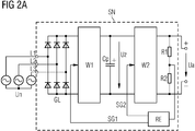
- FIG. 2a shows again by way of example in a schematic manner the switching power supply SN according to the invention consisting of the rectifier unit GL, the first converter stage W1 and the second, designed as a resonant converter converter stage W2. From the output voltage Ua of the second converter stage W2 or the resonant converter W2 can be derived either directly or with the aid of the voltage divider R1, R2, a feedback signal for the controller unit RE, wherein two or more manipulated variables SG1, SG2 to the two converter stage W1 and W2 be guided.
- the exemplary design variant for the switching power supply SN according to FIG. 2a a buffer capacitor Cp.
- the buffer capacitor Cp is inserted between the first converter stage W1 and the resonant converter W2. That is, the intermediate circuit between the two converter stages W1, W2 now has the buffer capacitor Cp, to which the intermediate circuit voltage Uz is applied as input voltage for the resonant converter W2.
- the buffer capacitor Cp for example, very short-term interruptions in the current and / or voltage supply can be bridged and the intermediate circuit voltage Uz can be kept constant. This is particularly true in the case of failure of a phase L1, L2, L3 of the three-phase AC power Un to fruition.
- the control for the resonant converter W2 is activated.
- a change in the switching frequency of the resonant converter W2 is performed for these time periods.
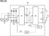
- FIG. 2b shows schematically and by way of example a variant of the inventive switching power supply SN according to FIG. 2a ,
- the regulator unit is divided into two subregulator units RE1, RE2, wherein the at least one manipulated variable SG2 for the regulation of the second converter stage W2 or of the resonant converter and of the second subregulator unit RE2 of the first subregulator RE1 the at least one manipulated variable SG1 for the control of the first Converter stage W1 is delivered.
- the signal for the regulation of the first converter stage W1 is derived, for example, from voltage or current information directly from the resonant converter W2, the voltage or current information providing information about the operating point of the resonant converter W2 (superresonant / in resonance / subresonant).
- the first sub-regulator unit RE1 regulates while the output voltage Ua of the switching power supply SN by frequency variation of the second converter stage W2 and the resonant converter. As a result, depending on the intermediate circuit voltage Uz, the second converter stage W2 can operate in a resonant, resonant or subresonant manner.
- the intermediate circuit voltage Uz is adjusted with the second subregulator unit RE2 until the converter stage W2 or the resonant converter can be operated substantially in resonance, ie with the resonant frequency with load-independent transmission ratio and thus with optimum efficiency.
- FIG. 3 shows schematically and by way of example a further advantageous embodiment of the switching power supply SN according to the invention, which can provide for example in case of failure of a phase L1, L2, L3 of the three-phase AC power supply Un for trouble-free operation of eg equipment.
- This embodiment of the switching power supply SN provides that an additional stage ZS is switchable in case of failure of a phase L1, L2, L3.
- the additional stage ZS is connected on the input side to the buffer capacitor Cp at the output of the first converter stage W1.
- the intermediate circuit voltage Uz thus forms the input voltage for the additional stage ZS when the additional stage ZS is activated.
- the additional stage ZS is connected to the second converter stage W2 or the resonant converter W2.
- auxiliary stage ZS When activated auxiliary stage ZS so that the output voltage of the additional stage ZS forms the input voltage for the resonant converter W2.
- the additional stage ZS is switched off in normal three-phase operation and is thereby bridged by a switching element such as a bypass diode BD, by which a current in the intermediate circuit is passed to the additional stage ZS.
- a switching element such as a bypass diode BD
- the bypass diode BD could be short-circuited in normal three-phase operation, for example by an active switch or a relay.
- the additional stage ZS can be activated.
- the activation is triggered by a drop in the intermediate circuit voltage Uz or the voltage across the buffer capacitor Cp, by an unwanted drop in the output voltage Ua or by a direct measurement of the phase voltages.
- the additional stage ZS or an active switch S1 for connecting the additional stage ZS is automatically controlled by the manipulated variable SG2 for those time ranges of the regulator unit RE with a predetermined frequency and a duty cycle in which the intermediate circuit voltage Uz decreases or no power supply due to a phase failure the input voltage of the switching power supply SN is available to keep the input voltage of the converter stage W2 and the resonant converter, and thus subsequently the output voltage Ua, constant.
- the predetermined frequency can be tracked in quasi-resonant or resonant control in a particular embodiment of the regulator unit RE, that the active switch S1 can always be turned on in a voltage minimum.
- the additional stage ZS can - as in FIG. 3 exemplified - be designed as boost converter.
- the second converter stage W2 and the resonant converter W2 also in the case of a phase failure continues to operate at the optimum operating point - ie at its resonant frequency at load-independent gear ratio.
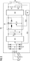
- FIG. 4 schematically shows a further, exemplary embodiment for an operation of the switching power supply SN in case of failure of a phase L1, L2, L3 of the three-phase supply voltage Un.
- a buffer capacitor Cx can be connected between the rectifier unit GL and the first converter stage W1.
- a control unit SE For the connection of the buffer capacitor Cx a control unit SE is provided, through which a switch S2 can be controlled. With the switch S2, depending on an output voltage of the rectifier unit GL, from which a signal for the control unit SE can be derived, for example, by means of a voltage divider, the buffer capacitor Cx can be connected as required. In this embodiment according to FIG. 4 However, it should be noted that the connection of the buffer capacitor Cx should take place in such a way that the supply network Un is not overstressed and an optional upstream fuse is not tripped.
Landscapes
- Engineering & Computer Science (AREA)
- Power Engineering (AREA)
- Dc-Dc Converters (AREA)
Priority Applications (4)
| Application Number | Priority Date | Filing Date | Title |
|---|---|---|---|
| EP16198690.6A EP3322076B1 (fr) | 2016-11-14 | 2016-11-14 | Alimentation à découpage comprenant un convertisseur à résonance |
| CN201780070302.8A CN110063007B (zh) | 2016-11-14 | 2017-10-05 | 具有谐振转换器的开关电源 |
| US16/349,671 US10944334B2 (en) | 2016-11-14 | 2017-10-05 | Switching power supply with resonant converter |
| PCT/EP2017/075334 WO2018086806A1 (fr) | 2016-11-14 | 2017-10-05 | Bloc d'alimentation à découpage à convertisseur à résonance |
Applications Claiming Priority (1)
| Application Number | Priority Date | Filing Date | Title |
|---|---|---|---|
| EP16198690.6A EP3322076B1 (fr) | 2016-11-14 | 2016-11-14 | Alimentation à découpage comprenant un convertisseur à résonance |
Publications (2)
| Publication Number | Publication Date |
|---|---|
| EP3322076A1 true EP3322076A1 (fr) | 2018-05-16 |
| EP3322076B1 EP3322076B1 (fr) | 2020-02-05 |
Family
ID=57288300
Family Applications (1)
| Application Number | Title | Priority Date | Filing Date |
|---|---|---|---|
| EP16198690.6A Active EP3322076B1 (fr) | 2016-11-14 | 2016-11-14 | Alimentation à découpage comprenant un convertisseur à résonance |
Country Status (4)
| Country | Link |
|---|---|
| US (1) | US10944334B2 (fr) |
| EP (1) | EP3322076B1 (fr) |
| CN (1) | CN110063007B (fr) |
| WO (1) | WO2018086806A1 (fr) |
Cited By (2)
| Publication number | Priority date | Publication date | Assignee | Title |
|---|---|---|---|---|
| CN116068927A (zh) * | 2021-11-03 | 2023-05-05 | 凹凸电子(武汉)有限公司 | 用于控制谐振变换器的控制器 |
| EP4607729A1 (fr) | 2024-02-23 | 2025-08-27 | Siemens Aktiengesellschaft | Procédé d'alimentation d'au moins une charge basse tension et dispositif électronique d'alimentation et/ou de distribution |
Families Citing this family (5)
| Publication number | Priority date | Publication date | Assignee | Title |
|---|---|---|---|---|
| JP7194654B2 (ja) * | 2019-08-09 | 2022-12-22 | Tvs Regza株式会社 | スイッチング電源装置 |
| CN112600396B (zh) * | 2020-12-31 | 2022-09-13 | 广州金升阳科技有限公司 | 一种反激变换器及其控制方法 |
| CN113824295B (zh) * | 2021-09-18 | 2025-06-13 | 广东汇芯半导体有限公司 | 半导体电路 |
| US12231044B2 (en) * | 2023-01-11 | 2025-02-18 | Apple Inc. | Power converter circuit for use with multiple low-current power rails |
| EP4525289A1 (fr) | 2023-09-14 | 2025-03-19 | FRONIUS INTERNATIONAL GmbH | Convertisseur résonant doté de demi-ponts d'entrée parallèles et procédé de commande d'un convertisseur résonant |
Citations (4)
| Publication number | Priority date | Publication date | Assignee | Title |
|---|---|---|---|---|
| US5563758A (en) * | 1994-02-22 | 1996-10-08 | International Business Machines Corporation | Circuit to permit three phase input power supply to operate when one phase drops out and provide lightening protection |
| US20060193153A1 (en) | 2004-12-20 | 2006-08-31 | Puls Gmbh | Power supply |
| US20090147553A1 (en) * | 2007-12-07 | 2009-06-11 | Samsung Electro-Mechanics Co., Ltd. | Dc power supply for varying output voltage according to load current variation |
| US20140104889A1 (en) * | 2012-10-12 | 2014-04-17 | Fuji Electric Co., Ltd. | Power supply device |
Family Cites Families (10)
| Publication number | Priority date | Publication date | Assignee | Title |
|---|---|---|---|---|
| PL346832A1 (en) * | 1998-09-18 | 2002-02-25 | Fls Miljo As | A method of operating an electrostatic precipitator |
| US7061212B2 (en) * | 2003-08-08 | 2006-06-13 | Astec International Limited | Circuit for maintaining hold-up time while reducing bulk capacitor size and improving efficiency in a power supply |
| US7375994B2 (en) * | 2005-10-11 | 2008-05-20 | Texas Instruments Incorporated | Highly efficient isolated AC/DC power conversion technique |
| US7888919B2 (en) * | 2008-03-20 | 2011-02-15 | International Business Machines Corporation | Apparatus, system, and method for an adaptive high efficiency switching power supply |
| US8687388B2 (en) * | 2012-01-31 | 2014-04-01 | Delta Electronics, Inc. | Three-phase soft-switched PFC rectifiers |
| JP5704124B2 (ja) * | 2012-06-14 | 2015-04-22 | 株式会社村田製作所 | スイッチング電源装置 |
| EP2928038A1 (fr) * | 2014-03-31 | 2015-10-07 | ABB Technology AG | Système de transfert d'énergie inductive et procédé de fonctionnement d'un système de transfert d'énergie inductive |
| US9473036B2 (en) * | 2014-06-05 | 2016-10-18 | Lite-On Electronics (Guangzhou) Limited | Direct current voltage conversion device |
| US9960686B2 (en) * | 2014-11-17 | 2018-05-01 | Infineon Technologies Austria Ag | System and method for detecting a loss of AC power in a switched-mode power supply |
| GB2540570B (en) * | 2015-07-21 | 2019-04-03 | Dyson Technology Ltd | Battery charger |
-
2016
- 2016-11-14 EP EP16198690.6A patent/EP3322076B1/fr active Active
-
2017
- 2017-10-05 WO PCT/EP2017/075334 patent/WO2018086806A1/fr not_active Ceased
- 2017-10-05 US US16/349,671 patent/US10944334B2/en active Active
- 2017-10-05 CN CN201780070302.8A patent/CN110063007B/zh active Active
Patent Citations (4)
| Publication number | Priority date | Publication date | Assignee | Title |
|---|---|---|---|---|
| US5563758A (en) * | 1994-02-22 | 1996-10-08 | International Business Machines Corporation | Circuit to permit three phase input power supply to operate when one phase drops out and provide lightening protection |
| US20060193153A1 (en) | 2004-12-20 | 2006-08-31 | Puls Gmbh | Power supply |
| US20090147553A1 (en) * | 2007-12-07 | 2009-06-11 | Samsung Electro-Mechanics Co., Ltd. | Dc power supply for varying output voltage according to load current variation |
| US20140104889A1 (en) * | 2012-10-12 | 2014-04-17 | Fuji Electric Co., Ltd. | Power supply device |
Cited By (3)
| Publication number | Priority date | Publication date | Assignee | Title |
|---|---|---|---|---|
| CN116068927A (zh) * | 2021-11-03 | 2023-05-05 | 凹凸电子(武汉)有限公司 | 用于控制谐振变换器的控制器 |
| EP4607729A1 (fr) | 2024-02-23 | 2025-08-27 | Siemens Aktiengesellschaft | Procédé d'alimentation d'au moins une charge basse tension et dispositif électronique d'alimentation et/ou de distribution |
| WO2025176493A1 (fr) | 2024-02-23 | 2025-08-28 | Siemens Aktiengesellschaft | Procédé d'alimentation d'au moins une charge basse tension et dispositif d'alimentation électronique et/ou de distribution d'énergie |
Also Published As
| Publication number | Publication date |
|---|---|
| CN110063007A (zh) | 2019-07-26 |
| CN110063007B (zh) | 2022-03-01 |
| US20190280612A1 (en) | 2019-09-12 |
| WO2018086806A1 (fr) | 2018-05-17 |
| US10944334B2 (en) | 2021-03-09 |
| EP3322076B1 (fr) | 2020-02-05 |
Similar Documents
| Publication | Publication Date | Title |
|---|---|---|
| EP3322076B1 (fr) | Alimentation à découpage comprenant un convertisseur à résonance | |
| EP3729623B1 (fr) | Dispositif convertisseur de tension comprenant un élément de réglage d'entrée et procédé permettant de faire fonctionner un dispositif convertisseur de tension | |
| EP2515424A2 (fr) | Convertisseur de tension continue | |
| DE102011011330B4 (de) | Tiefsetzsteller | |
| DE102007029388A1 (de) | Eigenstromversorgung für Stromrichterschaltertreiber | |
| DE102015211061A1 (de) | DC/DC-Wandler | |
| DE102016222367A1 (de) | Mehrphasen-Gleichstrom-Gleichstrom-Umsetzer mit asymmetrischem GM | |
| EP3563475B1 (fr) | Circuit convertisseur et procédé permettant de le commander | |
| DE102013114436A1 (de) | Elektrische Leistungsumwandlung mit asymmetrischer Phasenantwort | |
| EP3576284A1 (fr) | Couplage électrique d'un premier réseau électrique avec un second réseau électrique | |
| EP3525333A1 (fr) | Circuit convertisseur à oscillateur bloqué bidirectionnel | |
| DE102006033851A1 (de) | Wandler zur automatischen Verwendung | |
| EP2515425A2 (fr) | Convertisseur de tension continue | |
| EP1897213B1 (fr) | Bloc d'alimentation a circuit en pont integral et grande plage de reglage | |
| EP1647087B1 (fr) | Dispositif de commande servant a commander un commutateur de charge dans un regulateur a decoupage et procede pour commander un commutateur de charge | |
| CH714180B1 (de) | Konverter zur Übertragung von elektrischer Energie zwischen einem DC und einem AC-System. | |
| Neacsu et al. | A review and ultimate solution for output filters for high-power low-voltage DC/DC converters | |
| EP2228894A1 (fr) | Redresseur doté d'un circuit convertisseur à plusieurs niveaux | |
| DE102016222191A1 (de) | Asymetrischer zweistufiger Gleichstrom-Gleichstrom-Schaltumsetzer | |
| EP1532726B1 (fr) | Regulateur a decoupage | |
| WO2023066952A1 (fr) | Procédé de régulation d'un convertisseur résonnant | |
| EP2713489A1 (fr) | Procédé de fonctionnement d'un convertisseur PFC actif pendant puissance faible utilisant modulation fenêtre avec commande en boucle ouverte de largeur | |
| DE102018209139A1 (de) | Wechselspannungs-Ladevorrichtung | |
| EP1213820A2 (fr) | Convertisseur de tension pour plusieurs utilisateurs indépendants | |
| AT405228B (de) | Netzgleichrichterschaltung |
Legal Events
| Date | Code | Title | Description |
|---|---|---|---|
| PUAI | Public reference made under article 153(3) epc to a published international application that has entered the european phase |
Free format text: ORIGINAL CODE: 0009012 |
|
| STAA | Information on the status of an ep patent application or granted ep patent |
Free format text: STATUS: THE APPLICATION HAS BEEN PUBLISHED |
|
| AK | Designated contracting states |
Kind code of ref document: A1 Designated state(s): AL AT BE BG CH CY CZ DE DK EE ES FI FR GB GR HR HU IE IS IT LI LT LU LV MC MK MT NL NO PL PT RO RS SE SI SK SM TR |
|
| AX | Request for extension of the european patent |
Extension state: BA ME |
|
| STAA | Information on the status of an ep patent application or granted ep patent |
Free format text: STATUS: REQUEST FOR EXAMINATION WAS MADE |
|
| STAA | Information on the status of an ep patent application or granted ep patent |
Free format text: STATUS: EXAMINATION IS IN PROGRESS |
|
| 17P | Request for examination filed |
Effective date: 20181113 |
|
| RBV | Designated contracting states (corrected) |
Designated state(s): AL AT BE BG CH CY CZ DE DK EE ES FI FR GB GR HR HU IE IS IT LI LT LU LV MC MK MT NL NO PL PT RO RS SE SI SK SM TR |
|
| 17Q | First examination report despatched |
Effective date: 20181214 |
|
| GRAP | Despatch of communication of intention to grant a patent |
Free format text: ORIGINAL CODE: EPIDOSNIGR1 |
|
| STAA | Information on the status of an ep patent application or granted ep patent |
Free format text: STATUS: GRANT OF PATENT IS INTENDED |
|
| GRAJ | Information related to disapproval of communication of intention to grant by the applicant or resumption of examination proceedings by the epo deleted |
Free format text: ORIGINAL CODE: EPIDOSDIGR1 |
|
| STAA | Information on the status of an ep patent application or granted ep patent |
Free format text: STATUS: EXAMINATION IS IN PROGRESS |
|
| RIC1 | Information provided on ipc code assigned before grant |
Ipc: H02M 3/156 20060101ALI20190604BHEP Ipc: H02M 7/06 20060101ALI20190604BHEP Ipc: H02M 7/04 20060101AFI20190604BHEP Ipc: H02M 1/00 20060101ALN20190604BHEP |
|
| GRAP | Despatch of communication of intention to grant a patent |
Free format text: ORIGINAL CODE: EPIDOSNIGR1 |
|
| STAA | Information on the status of an ep patent application or granted ep patent |
Free format text: STATUS: GRANT OF PATENT IS INTENDED |
|
| INTG | Intention to grant announced |
Effective date: 20190621 |
|
| RIC1 | Information provided on ipc code assigned before grant |
Ipc: H02M 1/00 20060101ALN20190607BHEP Ipc: H02M 7/04 20060101AFI20190607BHEP Ipc: H02M 7/06 20060101ALI20190607BHEP Ipc: H02M 3/156 20060101ALI20190607BHEP |
|
| GRAJ | Information related to disapproval of communication of intention to grant by the applicant or resumption of examination proceedings by the epo deleted |
Free format text: ORIGINAL CODE: EPIDOSDIGR1 |
|
| GRAP | Despatch of communication of intention to grant a patent |
Free format text: ORIGINAL CODE: EPIDOSNIGR1 |
|
| INTC | Intention to grant announced (deleted) | ||
| GRAJ | Information related to disapproval of communication of intention to grant by the applicant or resumption of examination proceedings by the epo deleted |
Free format text: ORIGINAL CODE: EPIDOSDIGR1 |
|
| GRAP | Despatch of communication of intention to grant a patent |
Free format text: ORIGINAL CODE: EPIDOSNIGR1 |
|
| GRAJ | Information related to disapproval of communication of intention to grant by the applicant or resumption of examination proceedings by the epo deleted |
Free format text: ORIGINAL CODE: EPIDOSDIGR1 |
|
| GRAJ | Information related to disapproval of communication of intention to grant by the applicant or resumption of examination proceedings by the epo deleted |
Free format text: ORIGINAL CODE: EPIDOSDIGR1 |
|
| GRAP | Despatch of communication of intention to grant a patent |
Free format text: ORIGINAL CODE: EPIDOSNIGR1 |
|
| STAA | Information on the status of an ep patent application or granted ep patent |
Free format text: STATUS: EXAMINATION IS IN PROGRESS |
|
| RIC1 | Information provided on ipc code assigned before grant |
Ipc: H02M 1/00 20060101ALN20190703BHEP Ipc: H02M 7/06 20060101ALI20190703BHEP Ipc: H02M 3/156 20060101ALI20190703BHEP Ipc: H02M 7/04 20060101AFI20190703BHEP |
|
| GRAP | Despatch of communication of intention to grant a patent |
Free format text: ORIGINAL CODE: EPIDOSNIGR1 |
|
| GRAJ | Information related to disapproval of communication of intention to grant by the applicant or resumption of examination proceedings by the epo deleted |
Free format text: ORIGINAL CODE: EPIDOSDIGR1 |
|
| GRAP | Despatch of communication of intention to grant a patent |
Free format text: ORIGINAL CODE: EPIDOSNIGR1 |
|
| STAA | Information on the status of an ep patent application or granted ep patent |
Free format text: STATUS: GRANT OF PATENT IS INTENDED |
|
| GRAJ | Information related to disapproval of communication of intention to grant by the applicant or resumption of examination proceedings by the epo deleted |
Free format text: ORIGINAL CODE: EPIDOSDIGR1 |
|
| INTG | Intention to grant announced |
Effective date: 20190715 |
|
| GRAP | Despatch of communication of intention to grant a patent |
Free format text: ORIGINAL CODE: EPIDOSNIGR1 |
|
| REG | Reference to a national code |
Ref country code: DE Ref legal event code: R079 Ref document number: 502016008611 Country of ref document: DE Free format text: PREVIOUS MAIN CLASS: H02M0001000000 Ipc: H02M0007040000 |
|
| GRAJ | Information related to disapproval of communication of intention to grant by the applicant or resumption of examination proceedings by the epo deleted |
Free format text: ORIGINAL CODE: EPIDOSDIGR1 |
|
| INTG | Intention to grant announced |
Effective date: 20190801 |
|
| GRAP | Despatch of communication of intention to grant a patent |
Free format text: ORIGINAL CODE: EPIDOSNIGR1 |
|
| INTG | Intention to grant announced |
Effective date: 20190801 |
|
| INTC | Intention to grant announced (deleted) | ||
| INTG | Intention to grant announced |
Effective date: 20190822 |
|
| INTG | Intention to grant announced |
Effective date: 20190830 |
|
| RIC1 | Information provided on ipc code assigned before grant |
Ipc: H02M 3/156 20060101ALI20190822BHEP Ipc: H02M 7/06 20060101ALI20190822BHEP Ipc: H02M 7/04 20060101AFI20190822BHEP Ipc: H02M 1/00 20060101ALN20190822BHEP |
|
| GRAS | Grant fee paid |
Free format text: ORIGINAL CODE: EPIDOSNIGR3 |
|
| GRAA | (expected) grant |
Free format text: ORIGINAL CODE: 0009210 |
|
| STAA | Information on the status of an ep patent application or granted ep patent |
Free format text: STATUS: THE PATENT HAS BEEN GRANTED |
|
| AK | Designated contracting states |
Kind code of ref document: B1 Designated state(s): AL AT BE BG CH CY CZ DE DK EE ES FI FR GB GR HR HU IE IS IT LI LT LU LV MC MK MT NL NO PL PT RO RS SE SI SK SM TR |
|
| REG | Reference to a national code |
Ref country code: GB Ref legal event code: FG4D Free format text: NOT ENGLISH |
|
| REG | Reference to a national code |
Ref country code: AT Ref legal event code: REF Ref document number: 1230570 Country of ref document: AT Kind code of ref document: T Effective date: 20200215 |
|
| REG | Reference to a national code |
Ref country code: DE Ref legal event code: R096 Ref document number: 502016008611 Country of ref document: DE |
|
| REG | Reference to a national code |
Ref country code: IE Ref legal event code: FG4D Free format text: LANGUAGE OF EP DOCUMENT: GERMAN |
|
| REG | Reference to a national code |
Ref country code: CH Ref legal event code: EP |
|
| REG | Reference to a national code |
Ref country code: NL Ref legal event code: MP Effective date: 20200205 |
|
| PG25 | Lapsed in a contracting state [announced via postgrant information from national office to epo] |
Ref country code: RS Free format text: LAPSE BECAUSE OF FAILURE TO SUBMIT A TRANSLATION OF THE DESCRIPTION OR TO PAY THE FEE WITHIN THE PRESCRIBED TIME-LIMIT Effective date: 20200205 Ref country code: PT Free format text: LAPSE BECAUSE OF FAILURE TO SUBMIT A TRANSLATION OF THE DESCRIPTION OR TO PAY THE FEE WITHIN THE PRESCRIBED TIME-LIMIT Effective date: 20200628 Ref country code: NO Free format text: LAPSE BECAUSE OF FAILURE TO SUBMIT A TRANSLATION OF THE DESCRIPTION OR TO PAY THE FEE WITHIN THE PRESCRIBED TIME-LIMIT Effective date: 20200505 Ref country code: FI Free format text: LAPSE BECAUSE OF FAILURE TO SUBMIT A TRANSLATION OF THE DESCRIPTION OR TO PAY THE FEE WITHIN THE PRESCRIBED TIME-LIMIT Effective date: 20200205 |
|
| REG | Reference to a national code |
Ref country code: LT Ref legal event code: MG4D |
|
| PG25 | Lapsed in a contracting state [announced via postgrant information from national office to epo] |
Ref country code: HR Free format text: LAPSE BECAUSE OF FAILURE TO SUBMIT A TRANSLATION OF THE DESCRIPTION OR TO PAY THE FEE WITHIN THE PRESCRIBED TIME-LIMIT Effective date: 20200205 Ref country code: GR Free format text: LAPSE BECAUSE OF FAILURE TO SUBMIT A TRANSLATION OF THE DESCRIPTION OR TO PAY THE FEE WITHIN THE PRESCRIBED TIME-LIMIT Effective date: 20200506 Ref country code: BG Free format text: LAPSE BECAUSE OF FAILURE TO SUBMIT A TRANSLATION OF THE DESCRIPTION OR TO PAY THE FEE WITHIN THE PRESCRIBED TIME-LIMIT Effective date: 20200505 Ref country code: SE Free format text: LAPSE BECAUSE OF FAILURE TO SUBMIT A TRANSLATION OF THE DESCRIPTION OR TO PAY THE FEE WITHIN THE PRESCRIBED TIME-LIMIT Effective date: 20200205 Ref country code: IS Free format text: LAPSE BECAUSE OF FAILURE TO SUBMIT A TRANSLATION OF THE DESCRIPTION OR TO PAY THE FEE WITHIN THE PRESCRIBED TIME-LIMIT Effective date: 20200605 Ref country code: LV Free format text: LAPSE BECAUSE OF FAILURE TO SUBMIT A TRANSLATION OF THE DESCRIPTION OR TO PAY THE FEE WITHIN THE PRESCRIBED TIME-LIMIT Effective date: 20200205 |
|
| PG25 | Lapsed in a contracting state [announced via postgrant information from national office to epo] |
Ref country code: NL Free format text: LAPSE BECAUSE OF FAILURE TO SUBMIT A TRANSLATION OF THE DESCRIPTION OR TO PAY THE FEE WITHIN THE PRESCRIBED TIME-LIMIT Effective date: 20200205 |
|
| PG25 | Lapsed in a contracting state [announced via postgrant information from national office to epo] |
Ref country code: SK Free format text: LAPSE BECAUSE OF FAILURE TO SUBMIT A TRANSLATION OF THE DESCRIPTION OR TO PAY THE FEE WITHIN THE PRESCRIBED TIME-LIMIT Effective date: 20200205 Ref country code: RO Free format text: LAPSE BECAUSE OF FAILURE TO SUBMIT A TRANSLATION OF THE DESCRIPTION OR TO PAY THE FEE WITHIN THE PRESCRIBED TIME-LIMIT Effective date: 20200205 Ref country code: CZ Free format text: LAPSE BECAUSE OF FAILURE TO SUBMIT A TRANSLATION OF THE DESCRIPTION OR TO PAY THE FEE WITHIN THE PRESCRIBED TIME-LIMIT Effective date: 20200205 Ref country code: EE Free format text: LAPSE BECAUSE OF FAILURE TO SUBMIT A TRANSLATION OF THE DESCRIPTION OR TO PAY THE FEE WITHIN THE PRESCRIBED TIME-LIMIT Effective date: 20200205 Ref country code: SM Free format text: LAPSE BECAUSE OF FAILURE TO SUBMIT A TRANSLATION OF THE DESCRIPTION OR TO PAY THE FEE WITHIN THE PRESCRIBED TIME-LIMIT Effective date: 20200205 Ref country code: DK Free format text: LAPSE BECAUSE OF FAILURE TO SUBMIT A TRANSLATION OF THE DESCRIPTION OR TO PAY THE FEE WITHIN THE PRESCRIBED TIME-LIMIT Effective date: 20200205 Ref country code: LT Free format text: LAPSE BECAUSE OF FAILURE TO SUBMIT A TRANSLATION OF THE DESCRIPTION OR TO PAY THE FEE WITHIN THE PRESCRIBED TIME-LIMIT Effective date: 20200205 Ref country code: ES Free format text: LAPSE BECAUSE OF FAILURE TO SUBMIT A TRANSLATION OF THE DESCRIPTION OR TO PAY THE FEE WITHIN THE PRESCRIBED TIME-LIMIT Effective date: 20200205 |
|
| REG | Reference to a national code |
Ref country code: DE Ref legal event code: R097 Ref document number: 502016008611 Country of ref document: DE |
|
| PLBE | No opposition filed within time limit |
Free format text: ORIGINAL CODE: 0009261 |
|
| STAA | Information on the status of an ep patent application or granted ep patent |
Free format text: STATUS: NO OPPOSITION FILED WITHIN TIME LIMIT |
|
| 26N | No opposition filed |
Effective date: 20201106 |
|
| PG25 | Lapsed in a contracting state [announced via postgrant information from national office to epo] |
Ref country code: IT Free format text: LAPSE BECAUSE OF FAILURE TO SUBMIT A TRANSLATION OF THE DESCRIPTION OR TO PAY THE FEE WITHIN THE PRESCRIBED TIME-LIMIT Effective date: 20200205 |
|
| PG25 | Lapsed in a contracting state [announced via postgrant information from national office to epo] |
Ref country code: PL Free format text: LAPSE BECAUSE OF FAILURE TO SUBMIT A TRANSLATION OF THE DESCRIPTION OR TO PAY THE FEE WITHIN THE PRESCRIBED TIME-LIMIT Effective date: 20200205 Ref country code: SI Free format text: LAPSE BECAUSE OF FAILURE TO SUBMIT A TRANSLATION OF THE DESCRIPTION OR TO PAY THE FEE WITHIN THE PRESCRIBED TIME-LIMIT Effective date: 20200205 |
|
| REG | Reference to a national code |
Ref country code: CH Ref legal event code: NV Representative=s name: SIEMENS SCHWEIZ AG, CH |
|
| PG25 | Lapsed in a contracting state [announced via postgrant information from national office to epo] |
Ref country code: MC Free format text: LAPSE BECAUSE OF FAILURE TO SUBMIT A TRANSLATION OF THE DESCRIPTION OR TO PAY THE FEE WITHIN THE PRESCRIBED TIME-LIMIT Effective date: 20200205 |
|
| REG | Reference to a national code |
Ref country code: CH Ref legal event code: PL |
|
| GBPC | Gb: european patent ceased through non-payment of renewal fee |
Effective date: 20201114 |
|
| PG25 | Lapsed in a contracting state [announced via postgrant information from national office to epo] |
Ref country code: LU Free format text: LAPSE BECAUSE OF NON-PAYMENT OF DUE FEES Effective date: 20201114 |
|
| REG | Reference to a national code |
Ref country code: BE Ref legal event code: MM Effective date: 20201130 |
|
| PG25 | Lapsed in a contracting state [announced via postgrant information from national office to epo] |
Ref country code: CH Free format text: LAPSE BECAUSE OF NON-PAYMENT OF DUE FEES Effective date: 20201130 Ref country code: LI Free format text: LAPSE BECAUSE OF NON-PAYMENT OF DUE FEES Effective date: 20201130 |
|
| PG25 | Lapsed in a contracting state [announced via postgrant information from national office to epo] |
Ref country code: FR Free format text: LAPSE BECAUSE OF NON-PAYMENT OF DUE FEES Effective date: 20201130 Ref country code: IE Free format text: LAPSE BECAUSE OF NON-PAYMENT OF DUE FEES Effective date: 20201114 |
|
| PG25 | Lapsed in a contracting state [announced via postgrant information from national office to epo] |
Ref country code: GB Free format text: LAPSE BECAUSE OF NON-PAYMENT OF DUE FEES Effective date: 20201114 |
|
| PG25 | Lapsed in a contracting state [announced via postgrant information from national office to epo] |
Ref country code: TR Free format text: LAPSE BECAUSE OF FAILURE TO SUBMIT A TRANSLATION OF THE DESCRIPTION OR TO PAY THE FEE WITHIN THE PRESCRIBED TIME-LIMIT Effective date: 20200205 Ref country code: MT Free format text: LAPSE BECAUSE OF FAILURE TO SUBMIT A TRANSLATION OF THE DESCRIPTION OR TO PAY THE FEE WITHIN THE PRESCRIBED TIME-LIMIT Effective date: 20200205 Ref country code: CY Free format text: LAPSE BECAUSE OF FAILURE TO SUBMIT A TRANSLATION OF THE DESCRIPTION OR TO PAY THE FEE WITHIN THE PRESCRIBED TIME-LIMIT Effective date: 20200205 |
|
| PG25 | Lapsed in a contracting state [announced via postgrant information from national office to epo] |
Ref country code: MK Free format text: LAPSE BECAUSE OF FAILURE TO SUBMIT A TRANSLATION OF THE DESCRIPTION OR TO PAY THE FEE WITHIN THE PRESCRIBED TIME-LIMIT Effective date: 20200205 Ref country code: AL Free format text: LAPSE BECAUSE OF FAILURE TO SUBMIT A TRANSLATION OF THE DESCRIPTION OR TO PAY THE FEE WITHIN THE PRESCRIBED TIME-LIMIT Effective date: 20200205 |
|
| PG25 | Lapsed in a contracting state [announced via postgrant information from national office to epo] |
Ref country code: BE Free format text: LAPSE BECAUSE OF NON-PAYMENT OF DUE FEES Effective date: 20201130 |
|
| REG | Reference to a national code |
Ref country code: AT Ref legal event code: MM01 Ref document number: 1230570 Country of ref document: AT Kind code of ref document: T Effective date: 20211114 |
|
| PG25 | Lapsed in a contracting state [announced via postgrant information from national office to epo] |
Ref country code: AT Free format text: LAPSE BECAUSE OF NON-PAYMENT OF DUE FEES Effective date: 20211114 |
|
| PGFP | Annual fee paid to national office [announced via postgrant information from national office to epo] |
Ref country code: DE Payment date: 20260119 Year of fee payment: 10 |