EP3324331A1 - Kapazitive messschaltung - Google Patents
Kapazitive messschaltung Download PDFInfo
- Publication number
- EP3324331A1 EP3324331A1 EP16898879.8A EP16898879A EP3324331A1 EP 3324331 A1 EP3324331 A1 EP 3324331A1 EP 16898879 A EP16898879 A EP 16898879A EP 3324331 A1 EP3324331 A1 EP 3324331A1
- Authority
- EP
- European Patent Office
- Prior art keywords
- integrating
- circuit
- switch
- coupled
- capacitive sensing
- Prior art date
- Legal status (The legal status is an assumption and is not a legal conclusion. Google has not performed a legal analysis and makes no representation as to the accuracy of the status listed.)
- Granted
Links
Images
Classifications
-
- G—PHYSICS
- G06—COMPUTING OR CALCULATING; COUNTING
- G06V—IMAGE OR VIDEO RECOGNITION OR UNDERSTANDING
- G06V40/00—Recognition of biometric, human-related or animal-related patterns in image or video data
- G06V40/10—Human or animal bodies, e.g. vehicle occupants or pedestrians; Body parts, e.g. hands
- G06V40/12—Fingerprints or palmprints
- G06V40/13—Sensors therefor
- G06V40/1306—Sensors therefor non-optical, e.g. ultrasonic or capacitive sensing
-
- G—PHYSICS
- G06—COMPUTING OR CALCULATING; COUNTING
- G06V—IMAGE OR VIDEO RECOGNITION OR UNDERSTANDING
- G06V40/00—Recognition of biometric, human-related or animal-related patterns in image or video data
- G06V40/10—Human or animal bodies, e.g. vehicle occupants or pedestrians; Body parts, e.g. hands
- G06V40/12—Fingerprints or palmprints
- G06V40/1347—Preprocessing; Feature extraction
- G06V40/1359—Extracting features related to ridge properties; Determining the fingerprint type, e.g. whorl or loop
-
- H—ELECTRICITY
- H03—ELECTRONIC CIRCUITRY
- H03K—PULSE TECHNIQUE
- H03K17/00—Electronic switching or gating, i.e. not by contact-making and –breaking
- H03K17/94—Electronic switching or gating, i.e. not by contact-making and –breaking characterised by the way in which the control signals are generated
- H03K17/96—Touch switches
- H03K17/962—Capacitive touch switches
Definitions
- the present invention relates to a capacitive sensing circuit, and in particular, to a capacitive sensing circuit with a simple circuit configuration.
- a portable electronic device is generally used by an individual and it has a certain property of privacy, the data such as a telephone book, a photograph, personal information and the like stored therein is privately owned. If the electronic device is lost, the data may be used by others, resulting in unnecessary losses. While a manner of password protection has been used at present to avoid that the electronic device is used by others, a password is easy to be leaked or deciphered with lower security. Moreover, a user is required to remember the password when using an electronic device. If the password is forgotten, it will cause a lot of inconvenience. Therefore, a personal fingerprint identification system is developed currently to achieve identity authentication, so as to enhance data security.
- a capacitive sensing circuit is used to receive finger contact in a fingerprint identification system.
- the capacitive sensing circuit is used to accept finger contact and form a contact capacitor with a finger.
- the capacitive sensing circuit may convert a capacitance value of the contact capacitor into an analog voltage signal, which is converted into a digital voltage signal and then sent to a fingerprint determination module at a back end to determine finger ridges (Finger Ridge) or finger valleys (Finger Valley) of a fingerprint corresponding to the capacitive sensing circuit.
- the analog voltage signal is converted into the digital voltage signal through an analog-to-digital converter (Analog to Digital Convertor, ADC).
- a primary objective of the present invention is to provide a capacitive sensing circuit with a simple circuit structure.
- the present invention provides a capacitive sensing circuit, including a sample-and-hold circuit coupled to the contact capacitor; an integrating circuit including an integrating input terminal coupled to the sample-and-hold circuit and an integrating output terminal for outputting an integrating output voltage; a comparator including a first input terminal coupled to the integrating output terminal, a second input terminal for receiving a reference voltage, and a comparison output terminal; a counter coupled to the comparison output terminal and configured to accumulate a cumulative number of transitions of the comparator; a voltage boost circuit coupled to the integrating input terminal and configured to add a specific value to the integrating output voltage when the comparator performs a transition; and a logic circuit coupled to the counter, where the logic circuit outputs an integration time of the integrating circuit when the cumulative number is equal to a predetermined number, and the integration time correlates with a capacitance value of the contact capacitor.
- the logic circuit generates a control signal to terminate an integration operation of the integrating circuit when the cumulative number is equal to the predetermined number.
- the integration time is an elapsed time from start of the integration operation to termination of the integration operation of the integrating circuit.
- the sample-and-hold circuit includes a first switch having one end for receiving a positive voltage and the other end coupled to the contact capacitor; and a second switch having one end coupled to the contact capacitor and the other end coupled to the integrating input terminal, where the first switch is turned on and the second switch is turned off at a first time, and the first switch is turned off and the second switch is turned on at a second time.
- the integrating circuit includes an amplifier; a third switch coupled between the integrating input terminal and the integrating output terminal; an integrating capacitor coupled between the integrating input terminal and the integrating output terminal; and a fourth switch having one end coupled to the integrating capacitor and the other end coupled to the integrating output terminal.
- the third switch and the fourth switch are turned on when the capacitive sensing circuit is in a reset mode; and the third switch is turned off while the fourth switch is turned on when the integrating circuit performs an integration operation.
- the voltage boost circuit includes a boost capacitor coupled to the integrating input terminal; a fifth switch having one end for receiving a positive voltage and the other end coupled to the boost capacitor; and a sixth switch having one end for receiving a ground voltage and the other end coupled to the boost capacitor.
- the capacitive sensing circuit further includes a control circuit, where the control circuit controls that the fifth switch is turned on and the sixth switch is turned off at a first time; and the control circuit controls that the fifth switch is turned off and the sixth switch is turned on at a second time.
- the capacitive sensing circuit provided by the present invention may convert charge stored in the contact capacitor into a time signal, which has the advantages of simple circuit structure, small circuit area, low cost and low power consumption.
- a capacitive sensing circuit of the present invention converts charge stored in a contact capacitor into a time signal to accurately interpret a capacitance value of the contact capacitor and reduce circuit complexity of the capacitive sensing circuit.
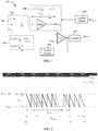
- FIG. 1 it is a schematic diagram of a capacitive sensing circuit 10 according to an embodiment of the present invention.
- the capacitive sensing circuit 10 is configured to sense a contact capacitor Cf and includes a sample-and-hold circuit SH, an integrating circuit 100, a comparator comp, a counter (cntr), a voltage boost circuit 104, a logic circuit 102 and a control circuit 106.
- the integrating circuit 100 includes switches S3 and S4, an amplifier Amp and an integrating capacitor C INT .
- An input terminal of the amplifier Amp is an integrating input terminal of the integrating circuit 100
- an output terminal of the amplifier Amp is an integrating output terminal of the integrating circuit 100, where the integrating output terminal is configured to output an integrating output voltage V OUT .
- a positive input terminal (labeled with "+") of the comparator (comp) is coupled to the integrating output terminal of the integrating circuit 100 and configured to receive the integrating output voltage V OUT
- a negative input terminal of the comparator (comp) (labeled with "-") is configured to receive a reference voltage V REF .
- a counter (cntr) is coupled to a comparison output terminal of the comparator (comp) and configured to accumulate a cumulative number N OUT of transitions of the comparator comp.
- the logic circuit 102 may be implemented by a digital circuit and it is coupled between the counter (cntr) and the integrating circuit 100.
- the logic circuit 102 When the cumulative number N OUT is equal to a predetermined number N TH , the logic circuit 102 outputs an integration time T OUT of the integrating circuit, and the logic circuit 102 generates a control signal (not shown in FIG. 1 ) and sends it to the integrating circuit 100 to terminate the integration operation of the integrating circuit 100, where the integration time T OUT may represent/reflect a capacitance value of the contact capacitor Cf.
- the sample-and-hold circuit SH includes a switch S1 and a switch S2.
- One end of the switch S1 receives a positive voltage V DD , and the other end of the switch S1 is electrically connected to the contact capacitor Cf; one end of the switch S2 is electrically connected to the contact capacitor Cf, and the other end of the switch S2 is electrically connected to the integrating input terminal of the integrating circuit 100.
- the switch S3 is coupled between the integrating input terminal and the integrating output terminal of the integrating circuit 100
- the integrating capacitor C INT is connected in series with the switch S4, and the integrating capacitor C INT and the switch S4 are also coupled between the integrating input terminal and the integrating output terminal of the integrating circuit 100.
- An operation mode of the integrating circuit 100 may be controlled by a conductive state of the control switches S3 and S4. For example, in a reset (Reset) mode of the capacitive sensing circuit 10, the switches S3 and S4 are turned on; in an integration mode of the capacitive sensing circuit 10 (i.e., when the integrating circuit 100 performs an integrating operation), the switch S3 is turned off and the switch S4 is turned on. If it needs to terminate the integration operation of the integrating circuit 100, the logic circuit 102 may generate a control signal to turn off the switch S4.
- the switch S1 When the integrating circuit 100 performs an integration operation (i.e., the integrating circuit 100 is operated in an integration mode), the switch S1 is turned on (ON) and the switch S2 is turned off (OFF) during a first half period (corresponding to a first time) of a clock (Clock) period T, and the contact capacitor Cf is charged to a positive voltage V DD ; the switch S1 is turned off and the switch S2 is turned on during a second half period (corresponding to a second time) of the clock period T, and charge stored in the contact capacitor Cf flows to the integrating capacitor C INT .
- the integrating output voltage V OUT decreases with time.
- the voltage boost circuit 104 includes switches S5 and S6 and a boost capacitor C DAC , where one end of the boost capacitor C DAC is coupled to the integrating input terminal and the other end is coupled to the switches S5 and S6.
- the switches S5 and S6 receive the positive voltage V DD and a ground voltage GND, respectively.
- the control circuit 106 is coupled between the voltage boost circuit 104 and the comparator output terminal of the comparator comp. When the integrating output voltage V OUT is less than a reference voltage V REF , the comparator (comp) performs a transition, and the control circuit 106 generates a control signal (not shown in FIG.
- the control circuit 106 controls that the switch S5 is turned on during a first half period (corresponding to a first time) of the clock period T' and is turned off during a second half period (corresponding to a second time) of the clock period T', and the switch S6 is turned off during the first half period of the clock period T' and is turned on during the second half of the clock period T'.
- the integrating output voltage V OUT is decreased due to integral, so that in an instant (i.e., during the clock period T') after that the integrating output voltage V OUT is less than the reference voltage V REF , the integrating output voltage V OUT may be increased to the voltage V REF +V K .
- a value of the integrating output voltage V OUT will be limited between the voltage V REF +V K and the voltage V REF .
- the integrating circuit 100 when the integrating circuit 100 performs an integration operation (i.e., the integrating circuit 100 is operated in an integration mode), the integrating output voltage V OUT is decreased to be less than the reference voltage V REF , the comparator (comp) performs a transition and the value of the counter (cntr) is incremented by 1.
- the control circuit 106 generates a control signal, such that a specific voltage value V K is added to the integrating output voltage V OUT (i.e., the integrating output voltage V OUT is increased to the voltage V REF +V K ).
- the integrating circuit 100 continues to integrate based on the increased voltage V REF +V K , i.e., the integrating output voltage V OUT is decreased continuously from the voltage V REF +V K until a next time that the integrating output voltage V OUT is less than the reference voltage V REF is achieved, the value of the counter (cntr) is incremented by 1 and the control circuit 106 generates a control signal again, so that a specific voltage value V K is added to the integrating output voltage V OUT again.
- the process is repeated until the logic circuit 102 determines that a cumulative number N OUT output by the counter (cntr) is equal to a predetermined number N TH , and the logic circuit 102 generates a control signal to terminate the integration operation of the integrating circuit 100 and outputs an integration time T OUT .
- a back end circuit (not shown in FIG. 1 ) of the capacitive sensing circuit 10 may determine the capacitance value of the contact capacitor Cf according to the integration time T OUT .
- FIG. 2 it is a waveform diagram of an integrating output voltage V OUT_1 and an integrating output voltage V OUT_2 generated by a capacitive sensing circuit 10 for capacitive sensing of a contact capacitor Cf_1 and a contact capacitor Cf_2, respectively, where the contact capacitor Cf_1 has a different capacitance value from the contact capacitor Cf_2.
- the dotted line represents the waveform of the integrating output voltage V OUT_1
- the solid line represents the waveform of the integrating output voltage V OUT_2 .
- the capacitive sensing circuit 10 starts an integration operation (or starts entering an integration mode) at a time t 0 .
- the comparator (comp) performs a transition over and over again until a time t 1 is achieved, i.e., when a cumulative number N OUT_1 accumulated by the counter (cntr) (corresponding to the contact capacitor Cf_1) reaches a predetermined number N TH , the logic circuit 102 outputs an integration time T OUT_1 (where the integration time T OUT_1 is a duration from the time to that the integrating circuit 100 starts an integration operation to the time t 1 that the integrating circuit 100 terminates the integration operation).
- the comparator (comp) performs a transition over and over again until a time t 2 is achieved, i.e., when a cumulative number N OUT_2 accumulated by the counter (cntr) (corresponding to the contact capacitor Cf_2) reaches the predetermined number N TH , the logic circuit 102 outputs an integration time T OUT_2 (where the integration time T OUT_1 is a duration from the time to that the integrating circuit 100 starts an integration operation to the time t 2 that the integrating circuit 100 terminates the integration operation).
- a back end circuit of the capacitive sensing circuit 10 may determine capacitance values of the contact capacitors Cf_1 and Cf_2 according to the integration times T OUT_1 and T OUT_2 , respectively.
- a voltage boost circuit 104 and a control circuit 106 are used to limit a value of an integrating output voltage V OUT between a voltage V REF +V K and a voltage V REF ; a counter (cntr) is used to calculate the number of transitions of a comparator comp; a logic circuit 102 is used to determine whether a cumulative number N OUT output by the counter (cntr) reaches a predetermined number N TH .
- the logic circuit 102 When the cumulative number N OUT reaches the predetermined number N TH , the logic circuit 102 outputs an integration time T OUT and a back end circuit of a capacitive sensing circuit 10 may determine a capacitance value of a contact capacitor Cf according to the integration time T OUT .
- ADC Analog to Digital Convertor
- the capacitive sensing circuit of the present invention converts charge stored in the contact capacitor into a time signal (i.e., an integration time T OUT ) without using an analog-to-digital converter, and a back end circuit may determine a capacitance value of the contact capacitor according to the integration time T OUT and then determine if there is a touch event, or determine finger ridges (Finger Ridge) or finger valleys (Finger Valley) of a fingerprint corresponding to a capacitive sensing circuit for fingerprint identification.
- a time signal i.e., an integration time T OUT
- a back end circuit may determine a capacitance value of the contact capacitor according to the integration time T OUT and then determine if there is a touch event, or determine finger ridges (Finger Ridge) or finger valleys (Finger Valley) of a fingerprint corresponding to a capacitive sensing circuit for fingerprint identification.
- a capacitive sensing circuit of the present invention may convert charge stored in a contact capacitor into a time signal without using a conventional analog-to-digital converter, and a capacitance value of the contact capacitor can be determined according to an integration time output by the capacitive sensing circuit of the present invention. Therefore, the capacitive sensing circuit of the present invention has advantages of simple circuit structure, small circuit area, low cost and low power consumption.
Landscapes
- Engineering & Computer Science (AREA)
- Human Computer Interaction (AREA)
- Physics & Mathematics (AREA)
- General Physics & Mathematics (AREA)
- Multimedia (AREA)
- Theoretical Computer Science (AREA)
- Computer Vision & Pattern Recognition (AREA)
- Analogue/Digital Conversion (AREA)
- Electronic Switches (AREA)
- Measurement Of Resistance Or Impedance (AREA)
Applications Claiming Priority (1)
| Application Number | Priority Date | Filing Date | Title |
|---|---|---|---|
| PCT/CN2016/100452 WO2018058335A1 (zh) | 2016-09-27 | 2016-09-27 | 电容感测电路 |
Publications (3)
| Publication Number | Publication Date |
|---|---|
| EP3324331A1 true EP3324331A1 (de) | 2018-05-23 |
| EP3324331A4 EP3324331A4 (de) | 2018-06-20 |
| EP3324331B1 EP3324331B1 (de) | 2020-11-25 |
Family
ID=58839093
Family Applications (1)
| Application Number | Title | Priority Date | Filing Date |
|---|---|---|---|
| EP16898879.8A Not-in-force EP3324331B1 (de) | 2016-09-27 | 2016-09-27 | Kapazitive messschaltung |
Country Status (5)
| Country | Link |
|---|---|
| US (1) | US10565420B2 (de) |
| EP (1) | EP3324331B1 (de) |
| KR (1) | KR102032890B1 (de) |
| CN (1) | CN106663200A (de) |
| WO (1) | WO2018058335A1 (de) |
Families Citing this family (8)
| Publication number | Priority date | Publication date | Assignee | Title |
|---|---|---|---|---|
| WO2018094579A1 (zh) | 2016-11-22 | 2018-05-31 | 深圳市汇顶科技股份有限公司 | 电容感测电路及指纹辨识系统 |
| WO2019084832A1 (zh) * | 2017-11-01 | 2019-05-09 | 深圳市汇顶科技股份有限公司 | 一种指纹识别电路、指纹传感器及移动终端 |
| US11067672B2 (en) | 2018-06-19 | 2021-07-20 | Waymo Llc | Shared sample and convert capacitor architecture |
| CN111162768B (zh) * | 2018-11-07 | 2023-01-31 | 台达电子工业股份有限公司 | 控制装置及方法 |
| WO2021203418A1 (zh) * | 2020-04-10 | 2021-10-14 | 京东方科技集团股份有限公司 | 指纹识别检测电路及其控制方法、指纹识别控制芯片 |
| GB202014008D0 (en) | 2020-09-07 | 2020-10-21 | Touch Biometrix Ltd | Biometric skin contact sensor and methods of operating a biometric skin contact sensor |
| GB202014049D0 (en) | 2020-09-07 | 2020-10-21 | Touch Biometrix Ltd | Biometric skin contact sensor and methods of operating a biometric skin contact sensor |
| GB202014011D0 (en) | 2020-09-07 | 2020-10-21 | Touch Biometrix Ltd | Biometric skin contact sensor and methods of operating a biometric skin contact sensor |
Family Cites Families (26)
| Publication number | Priority date | Publication date | Assignee | Title |
|---|---|---|---|---|
| US7062075B2 (en) | 2001-05-14 | 2006-06-13 | Nippon Telegraph And Telephone Corporation | Surface shape recognition sensor device |
| JP2003028607A (ja) * | 2001-07-12 | 2003-01-29 | Sony Corp | 静電容量検出装置およびこれを用いた指紋照合装置 |
| JP2003090703A (ja) * | 2001-07-12 | 2003-03-28 | Sharp Corp | 凹凸パターン検出器および凹凸パターン検出方法 |
| US6636053B1 (en) * | 2001-11-02 | 2003-10-21 | Stmicroelectronics, Inc. | Capacitive pixel for fingerprint sensor |
| US7965877B2 (en) * | 2005-10-24 | 2011-06-21 | Baohua Qi | Fingerprint sensing device using pulse processing |
| US7511648B2 (en) * | 2007-04-23 | 2009-03-31 | Texas Instruments Incorporated | Integrating/SAR ADC and method with low integrator swing and low complexity |
| TWI381173B (zh) * | 2008-10-29 | 2013-01-01 | Raydium Semiconductor Corp | 電容量測電路及其電容量測方法 |
| CN102200869B (zh) * | 2010-03-24 | 2013-05-08 | 盛群半导体股份有限公司 | 电容式触控装置及其感测装置 |
| CN103138762B (zh) * | 2011-11-30 | 2016-04-27 | 禾瑞亚科技股份有限公司 | 多阶取样保持电路 |
| US9740343B2 (en) * | 2012-04-13 | 2017-08-22 | Apple Inc. | Capacitive sensing array modulation |
| CN102954753B (zh) * | 2012-10-22 | 2015-09-09 | 苏州迈瑞微电子有限公司 | 电容式距离传感器 |
| CN102957404B (zh) * | 2012-10-22 | 2015-09-09 | 苏州迈瑞微电子有限公司 | 边沿时间读出电路 |
| CN103837163A (zh) * | 2012-11-26 | 2014-06-04 | 矽创电子股份有限公司 | 电容感测电路 |
| US8982093B2 (en) * | 2012-12-20 | 2015-03-17 | Broadcom Corporation | Capacitive touch sensing system with interference rejection |
| US9164137B2 (en) * | 2013-12-05 | 2015-10-20 | Parade Technologies, Ltd. | Tunable baseline compensation scheme for touchscreen controllers |
| CN103714330B (zh) | 2014-01-06 | 2017-12-19 | 苏州迈瑞微电子有限公司 | 电容指纹传感器 |
| KR101881682B1 (ko) * | 2014-10-13 | 2018-07-24 | 선전 구딕스 테크놀로지 컴퍼니, 리미티드 | 지문 인식용 센서 픽셀 회로 |
| CN105046194B (zh) * | 2015-06-08 | 2020-04-10 | 苏州迈瑞微电子有限公司 | 一种包含积分器的电容指纹传感器 |
| WO2017076292A1 (en) * | 2015-11-02 | 2017-05-11 | Shenzhen Huiding Technology Co., Ltd. | Multifunction fingerprint sensor having optical sensing against fingerprint spoofing |
| CN107003347B (zh) * | 2015-10-23 | 2019-12-17 | 深圳市汇顶科技股份有限公司 | 电容检测传感器及其相关装置和系统 |
| SE1650548A1 (en) * | 2016-04-22 | 2017-10-23 | Fingerprint Cards Ab | Fingerprint sensing system with sensing reference potential providing circuitry |
| SE539638C2 (en) * | 2016-04-22 | 2017-10-24 | Fingerprint Cards Ab | Fingerprint sensing system with adaptive power control |
| US10121048B2 (en) * | 2016-07-29 | 2018-11-06 | Elan Microelectronics Corporation | Operating method for a fingerprint sensing device and fingerprint sensing system |
| CN106796658A (zh) * | 2016-11-21 | 2017-05-31 | 深圳市汇顶科技股份有限公司 | 指纹传感器及电子终端 |
| US10346665B2 (en) * | 2017-05-30 | 2019-07-09 | Sunasic Technologies Limited | Noise reduced capacitive image sensor and method operating the same |
| US10205895B2 (en) * | 2017-07-05 | 2019-02-12 | Sunasic Technologies Limited | Capacitive image sensor with noise reduction feature and method operating the same |
-
2016
- 2016-09-27 CN CN201680001054.7A patent/CN106663200A/zh active Pending
- 2016-09-27 KR KR1020177029860A patent/KR102032890B1/ko not_active Expired - Fee Related
- 2016-09-27 WO PCT/CN2016/100452 patent/WO2018058335A1/zh not_active Ceased
- 2016-09-27 EP EP16898879.8A patent/EP3324331B1/de not_active Not-in-force
-
2017
- 2017-10-13 US US15/784,075 patent/US10565420B2/en not_active Expired - Fee Related
Also Published As
| Publication number | Publication date |
|---|---|
| US20180089490A1 (en) | 2018-03-29 |
| US10565420B2 (en) | 2020-02-18 |
| KR20180048446A (ko) | 2018-05-10 |
| EP3324331A4 (de) | 2018-06-20 |
| WO2018058335A1 (zh) | 2018-04-05 |
| CN106663200A (zh) | 2017-05-10 |
| EP3324331B1 (de) | 2020-11-25 |
| KR102032890B1 (ko) | 2019-10-16 |
Similar Documents
| Publication | Publication Date | Title |
|---|---|---|
| US10346668B2 (en) | Capacitive sensing circuit | |
| US10565420B2 (en) | Capacitive sensing circuit | |
| US9400912B2 (en) | Capacitive fingerprint sensor and fingerprint sensing method thereof | |
| EP3351948B1 (de) | Kapazitätsmessschaltung und fingerabdruckidentifizierungssystem | |
| WO2017067108A1 (zh) | 信号转换电路及指纹识别系统 | |
| CN107797694A (zh) | 一种积分电路设备及其操作方法 | |
| WO2018201432A1 (zh) | 电压转换装置和指纹检测系统 | |
| WO2017016103A1 (zh) | 指纹检测电路及指纹辨识系统 | |
| CN110084082A (zh) | 一种电子设备、指纹识别装置及其手指触摸检测电路 | |
| CN102262487B (zh) | 触控面板的切换式电容追踪装置及其操作方法 | |
| EP3206159A1 (de) | Ausgangsumwandlungsschaltung und fingerabdruckerkennungssystem | |
| CN106462760B (zh) | 指纹辨识系统 | |
| CN103312340A (zh) | 电路及实现键盘的方法 |
Legal Events
| Date | Code | Title | Description |
|---|---|---|---|
| STAA | Information on the status of an ep patent application or granted ep patent |
Free format text: STATUS: UNKNOWN |
|
| STAA | Information on the status of an ep patent application or granted ep patent |
Free format text: STATUS: THE INTERNATIONAL PUBLICATION HAS BEEN MADE |
|
| PUAI | Public reference made under article 153(3) epc to a published international application that has entered the european phase |
Free format text: ORIGINAL CODE: 0009012 |
|
| STAA | Information on the status of an ep patent application or granted ep patent |
Free format text: STATUS: REQUEST FOR EXAMINATION WAS MADE |
|
| 17P | Request for examination filed |
Effective date: 20171027 |
|
| AK | Designated contracting states |
Kind code of ref document: A1 Designated state(s): AL AT BE BG CH CY CZ DE DK EE ES FI FR GB GR HR HU IE IS IT LI LT LU LV MC MK MT NL NO PL PT RO RS SE SI SK SM TR |
|
| AX | Request for extension of the european patent |
Extension state: BA ME |
|
| A4 | Supplementary search report drawn up and despatched |
Effective date: 20180522 |
|
| RIC1 | Information provided on ipc code assigned before grant |
Ipc: G06K 9/00 20060101AFI20180515BHEP |
|
| STAA | Information on the status of an ep patent application or granted ep patent |
Free format text: STATUS: EXAMINATION IS IN PROGRESS |
|
| 17Q | First examination report despatched |
Effective date: 20190305 |
|
| DAV | Request for validation of the european patent (deleted) | ||
| DAX | Request for extension of the european patent (deleted) | ||
| GRAP | Despatch of communication of intention to grant a patent |
Free format text: ORIGINAL CODE: EPIDOSNIGR1 |
|
| STAA | Information on the status of an ep patent application or granted ep patent |
Free format text: STATUS: GRANT OF PATENT IS INTENDED |
|
| INTG | Intention to grant announced |
Effective date: 20200819 |
|
| GRAS | Grant fee paid |
Free format text: ORIGINAL CODE: EPIDOSNIGR3 |
|
| GRAA | (expected) grant |
Free format text: ORIGINAL CODE: 0009210 |
|
| STAA | Information on the status of an ep patent application or granted ep patent |
Free format text: STATUS: THE PATENT HAS BEEN GRANTED |
|
| AK | Designated contracting states |
Kind code of ref document: B1 Designated state(s): AL AT BE BG CH CY CZ DE DK EE ES FI FR GB GR HR HU IE IS IT LI LT LU LV MC MK MT NL NO PL PT RO RS SE SI SK SM TR |
|
| REG | Reference to a national code |
Ref country code: GB Ref legal event code: FG4D |
|
| REG | Reference to a national code |
Ref country code: CH Ref legal event code: EP |
|
| REG | Reference to a national code |
Ref country code: AT Ref legal event code: REF Ref document number: 1339132 Country of ref document: AT Kind code of ref document: T Effective date: 20201215 |
|
| REG | Reference to a national code |
Ref country code: DE Ref legal event code: R096 Ref document number: 602016048844 Country of ref document: DE |
|
| REG | Reference to a national code |
Ref country code: IE Ref legal event code: FG4D |
|
| REG | Reference to a national code |
Ref country code: AT Ref legal event code: MK05 Ref document number: 1339132 Country of ref document: AT Kind code of ref document: T Effective date: 20201125 |
|
| REG | Reference to a national code |
Ref country code: NL Ref legal event code: MP Effective date: 20201125 |
|
| PG25 | Lapsed in a contracting state [announced via postgrant information from national office to epo] |
Ref country code: NO Free format text: LAPSE BECAUSE OF FAILURE TO SUBMIT A TRANSLATION OF THE DESCRIPTION OR TO PAY THE FEE WITHIN THE PRESCRIBED TIME-LIMIT Effective date: 20210225 Ref country code: PT Free format text: LAPSE BECAUSE OF FAILURE TO SUBMIT A TRANSLATION OF THE DESCRIPTION OR TO PAY THE FEE WITHIN THE PRESCRIBED TIME-LIMIT Effective date: 20210325 Ref country code: RS Free format text: LAPSE BECAUSE OF FAILURE TO SUBMIT A TRANSLATION OF THE DESCRIPTION OR TO PAY THE FEE WITHIN THE PRESCRIBED TIME-LIMIT Effective date: 20201125 Ref country code: FI Free format text: LAPSE BECAUSE OF FAILURE TO SUBMIT A TRANSLATION OF THE DESCRIPTION OR TO PAY THE FEE WITHIN THE PRESCRIBED TIME-LIMIT Effective date: 20201125 Ref country code: GR Free format text: LAPSE BECAUSE OF FAILURE TO SUBMIT A TRANSLATION OF THE DESCRIPTION OR TO PAY THE FEE WITHIN THE PRESCRIBED TIME-LIMIT Effective date: 20210226 |
|
| PG25 | Lapsed in a contracting state [announced via postgrant information from national office to epo] |
Ref country code: AT Free format text: LAPSE BECAUSE OF FAILURE TO SUBMIT A TRANSLATION OF THE DESCRIPTION OR TO PAY THE FEE WITHIN THE PRESCRIBED TIME-LIMIT Effective date: 20201125 Ref country code: BG Free format text: LAPSE BECAUSE OF FAILURE TO SUBMIT A TRANSLATION OF THE DESCRIPTION OR TO PAY THE FEE WITHIN THE PRESCRIBED TIME-LIMIT Effective date: 20210225 Ref country code: LV Free format text: LAPSE BECAUSE OF FAILURE TO SUBMIT A TRANSLATION OF THE DESCRIPTION OR TO PAY THE FEE WITHIN THE PRESCRIBED TIME-LIMIT Effective date: 20201125 Ref country code: IS Free format text: LAPSE BECAUSE OF FAILURE TO SUBMIT A TRANSLATION OF THE DESCRIPTION OR TO PAY THE FEE WITHIN THE PRESCRIBED TIME-LIMIT Effective date: 20210325 Ref country code: PL Free format text: LAPSE BECAUSE OF FAILURE TO SUBMIT A TRANSLATION OF THE DESCRIPTION OR TO PAY THE FEE WITHIN THE PRESCRIBED TIME-LIMIT Effective date: 20201125 Ref country code: SE Free format text: LAPSE BECAUSE OF FAILURE TO SUBMIT A TRANSLATION OF THE DESCRIPTION OR TO PAY THE FEE WITHIN THE PRESCRIBED TIME-LIMIT Effective date: 20201125 |
|
| REG | Reference to a national code |
Ref country code: LT Ref legal event code: MG9D |
|
| PG25 | Lapsed in a contracting state [announced via postgrant information from national office to epo] |
Ref country code: HR Free format text: LAPSE BECAUSE OF FAILURE TO SUBMIT A TRANSLATION OF THE DESCRIPTION OR TO PAY THE FEE WITHIN THE PRESCRIBED TIME-LIMIT Effective date: 20201125 |
|
| PG25 | Lapsed in a contracting state [announced via postgrant information from national office to epo] |
Ref country code: RO Free format text: LAPSE BECAUSE OF FAILURE TO SUBMIT A TRANSLATION OF THE DESCRIPTION OR TO PAY THE FEE WITHIN THE PRESCRIBED TIME-LIMIT Effective date: 20201125 Ref country code: SK Free format text: LAPSE BECAUSE OF FAILURE TO SUBMIT A TRANSLATION OF THE DESCRIPTION OR TO PAY THE FEE WITHIN THE PRESCRIBED TIME-LIMIT Effective date: 20201125 Ref country code: LT Free format text: LAPSE BECAUSE OF FAILURE TO SUBMIT A TRANSLATION OF THE DESCRIPTION OR TO PAY THE FEE WITHIN THE PRESCRIBED TIME-LIMIT Effective date: 20201125 Ref country code: SM Free format text: LAPSE BECAUSE OF FAILURE TO SUBMIT A TRANSLATION OF THE DESCRIPTION OR TO PAY THE FEE WITHIN THE PRESCRIBED TIME-LIMIT Effective date: 20201125 Ref country code: CZ Free format text: LAPSE BECAUSE OF FAILURE TO SUBMIT A TRANSLATION OF THE DESCRIPTION OR TO PAY THE FEE WITHIN THE PRESCRIBED TIME-LIMIT Effective date: 20201125 Ref country code: EE Free format text: LAPSE BECAUSE OF FAILURE TO SUBMIT A TRANSLATION OF THE DESCRIPTION OR TO PAY THE FEE WITHIN THE PRESCRIBED TIME-LIMIT Effective date: 20201125 |
|
| REG | Reference to a national code |
Ref country code: DE Ref legal event code: R097 Ref document number: 602016048844 Country of ref document: DE |
|
| PG25 | Lapsed in a contracting state [announced via postgrant information from national office to epo] |
Ref country code: DK Free format text: LAPSE BECAUSE OF FAILURE TO SUBMIT A TRANSLATION OF THE DESCRIPTION OR TO PAY THE FEE WITHIN THE PRESCRIBED TIME-LIMIT Effective date: 20201125 |
|
| PLBE | No opposition filed within time limit |
Free format text: ORIGINAL CODE: 0009261 |
|
| STAA | Information on the status of an ep patent application or granted ep patent |
Free format text: STATUS: NO OPPOSITION FILED WITHIN TIME LIMIT |
|
| PG25 | Lapsed in a contracting state [announced via postgrant information from national office to epo] |
Ref country code: IT Free format text: LAPSE BECAUSE OF FAILURE TO SUBMIT A TRANSLATION OF THE DESCRIPTION OR TO PAY THE FEE WITHIN THE PRESCRIBED TIME-LIMIT Effective date: 20201125 Ref country code: NL Free format text: LAPSE BECAUSE OF FAILURE TO SUBMIT A TRANSLATION OF THE DESCRIPTION OR TO PAY THE FEE WITHIN THE PRESCRIBED TIME-LIMIT Effective date: 20201125 Ref country code: AL Free format text: LAPSE BECAUSE OF FAILURE TO SUBMIT A TRANSLATION OF THE DESCRIPTION OR TO PAY THE FEE WITHIN THE PRESCRIBED TIME-LIMIT Effective date: 20201125 |
|
| 26N | No opposition filed |
Effective date: 20210826 |
|
| REG | Reference to a national code |
Ref country code: DE Ref legal event code: R079 Ref document number: 602016048844 Country of ref document: DE Free format text: PREVIOUS MAIN CLASS: G06K0009000000 Ipc: G06V0010000000 |
|
| PG25 | Lapsed in a contracting state [announced via postgrant information from national office to epo] |
Ref country code: SI Free format text: LAPSE BECAUSE OF FAILURE TO SUBMIT A TRANSLATION OF THE DESCRIPTION OR TO PAY THE FEE WITHIN THE PRESCRIBED TIME-LIMIT Effective date: 20201125 |
|
| PG25 | Lapsed in a contracting state [announced via postgrant information from national office to epo] |
Ref country code: ES Free format text: LAPSE BECAUSE OF FAILURE TO SUBMIT A TRANSLATION OF THE DESCRIPTION OR TO PAY THE FEE WITHIN THE PRESCRIBED TIME-LIMIT Effective date: 20201125 |
|
| REG | Reference to a national code |
Ref country code: CH Ref legal event code: PL |
|
| REG | Reference to a national code |
Ref country code: BE Ref legal event code: MM Effective date: 20210930 |
|
| PG25 | Lapsed in a contracting state [announced via postgrant information from national office to epo] |
Ref country code: IS Free format text: LAPSE BECAUSE OF FAILURE TO SUBMIT A TRANSLATION OF THE DESCRIPTION OR TO PAY THE FEE WITHIN THE PRESCRIBED TIME-LIMIT Effective date: 20210325 Ref country code: MC Free format text: LAPSE BECAUSE OF FAILURE TO SUBMIT A TRANSLATION OF THE DESCRIPTION OR TO PAY THE FEE WITHIN THE PRESCRIBED TIME-LIMIT Effective date: 20201125 |
|
| PG25 | Lapsed in a contracting state [announced via postgrant information from national office to epo] |
Ref country code: LU Free format text: LAPSE BECAUSE OF NON-PAYMENT OF DUE FEES Effective date: 20210927 Ref country code: IE Free format text: LAPSE BECAUSE OF NON-PAYMENT OF DUE FEES Effective date: 20210927 Ref country code: FR Free format text: LAPSE BECAUSE OF NON-PAYMENT OF DUE FEES Effective date: 20210930 Ref country code: BE Free format text: LAPSE BECAUSE OF NON-PAYMENT OF DUE FEES Effective date: 20210930 |
|
| PG25 | Lapsed in a contracting state [announced via postgrant information from national office to epo] |
Ref country code: LI Free format text: LAPSE BECAUSE OF NON-PAYMENT OF DUE FEES Effective date: 20210930 Ref country code: CH Free format text: LAPSE BECAUSE OF NON-PAYMENT OF DUE FEES Effective date: 20210930 |
|
| PGFP | Annual fee paid to national office [announced via postgrant information from national office to epo] |
Ref country code: GB Payment date: 20220920 Year of fee payment: 7 Ref country code: DE Payment date: 20220920 Year of fee payment: 7 |
|
| PG25 | Lapsed in a contracting state [announced via postgrant information from national office to epo] |
Ref country code: HU Free format text: LAPSE BECAUSE OF FAILURE TO SUBMIT A TRANSLATION OF THE DESCRIPTION OR TO PAY THE FEE WITHIN THE PRESCRIBED TIME-LIMIT; INVALID AB INITIO Effective date: 20160927 |
|
| PG25 | Lapsed in a contracting state [announced via postgrant information from national office to epo] |
Ref country code: CY Free format text: LAPSE BECAUSE OF FAILURE TO SUBMIT A TRANSLATION OF THE DESCRIPTION OR TO PAY THE FEE WITHIN THE PRESCRIBED TIME-LIMIT Effective date: 20201125 |
|
| REG | Reference to a national code |
Ref country code: DE Ref legal event code: R119 Ref document number: 602016048844 Country of ref document: DE |
|
| PG25 | Lapsed in a contracting state [announced via postgrant information from national office to epo] |
Ref country code: MK Free format text: LAPSE BECAUSE OF FAILURE TO SUBMIT A TRANSLATION OF THE DESCRIPTION OR TO PAY THE FEE WITHIN THE PRESCRIBED TIME-LIMIT Effective date: 20201125 |
|
| GBPC | Gb: european patent ceased through non-payment of renewal fee |
Effective date: 20230927 |
|
| PG25 | Lapsed in a contracting state [announced via postgrant information from national office to epo] |
Ref country code: GB Free format text: LAPSE BECAUSE OF NON-PAYMENT OF DUE FEES Effective date: 20230927 |
|
| PG25 | Lapsed in a contracting state [announced via postgrant information from national office to epo] |
Ref country code: GB Free format text: LAPSE BECAUSE OF NON-PAYMENT OF DUE FEES Effective date: 20230927 Ref country code: DE Free format text: LAPSE BECAUSE OF NON-PAYMENT OF DUE FEES Effective date: 20240403 |
|
| PG25 | Lapsed in a contracting state [announced via postgrant information from national office to epo] |
Ref country code: MT Free format text: LAPSE BECAUSE OF FAILURE TO SUBMIT A TRANSLATION OF THE DESCRIPTION OR TO PAY THE FEE WITHIN THE PRESCRIBED TIME-LIMIT Effective date: 20201125 |
|
| PG25 | Lapsed in a contracting state [announced via postgrant information from national office to epo] |
Ref country code: TR Free format text: LAPSE BECAUSE OF FAILURE TO SUBMIT A TRANSLATION OF THE DESCRIPTION OR TO PAY THE FEE WITHIN THE PRESCRIBED TIME-LIMIT Effective date: 20201125 |