EP3324447A1 - Cellule solaire - Google Patents
Cellule solaire Download PDFInfo
- Publication number
- EP3324447A1 EP3324447A1 EP17210606.4A EP17210606A EP3324447A1 EP 3324447 A1 EP3324447 A1 EP 3324447A1 EP 17210606 A EP17210606 A EP 17210606A EP 3324447 A1 EP3324447 A1 EP 3324447A1
- Authority
- EP
- European Patent Office
- Prior art keywords
- transparent conductive
- conductive layer
- layer
- solar cell
- thickness
- Prior art date
- Legal status (The legal status is an assumption and is not a legal conclusion. Google has not performed a legal analysis and makes no representation as to the accuracy of the status listed.)
- Granted
Links
Images

Classifications
-
- H—ELECTRICITY
- H10—SEMICONDUCTOR DEVICES; ELECTRIC SOLID-STATE DEVICES NOT OTHERWISE PROVIDED FOR
- H10F—INORGANIC SEMICONDUCTOR DEVICES SENSITIVE TO INFRARED RADIATION, LIGHT, ELECTROMAGNETIC RADIATION OF SHORTER WAVELENGTH OR CORPUSCULAR RADIATION
- H10F77/00—Constructional details of devices covered by this subclass
- H10F77/20—Electrodes
- H10F77/206—Electrodes for devices having potential barriers
- H10F77/211—Electrodes for devices having potential barriers for photovoltaic cells
- H10F77/219—Arrangements for electrodes of back-contact photovoltaic cells
- H10F77/223—Arrangements for electrodes of back-contact photovoltaic cells for metallisation wrap-through [MWT] photovoltaic cells
-
- H—ELECTRICITY
- H10—SEMICONDUCTOR DEVICES; ELECTRIC SOLID-STATE DEVICES NOT OTHERWISE PROVIDED FOR
- H10F—INORGANIC SEMICONDUCTOR DEVICES SENSITIVE TO INFRARED RADIATION, LIGHT, ELECTROMAGNETIC RADIATION OF SHORTER WAVELENGTH OR CORPUSCULAR RADIATION
- H10F10/00—Individual photovoltaic cells, e.g. solar cells
- H10F10/10—Individual photovoltaic cells, e.g. solar cells having potential barriers
- H10F10/16—Photovoltaic cells having only PN heterojunction potential barriers
-
- H—ELECTRICITY
- H10—SEMICONDUCTOR DEVICES; ELECTRIC SOLID-STATE DEVICES NOT OTHERWISE PROVIDED FOR
- H10F—INORGANIC SEMICONDUCTOR DEVICES SENSITIVE TO INFRARED RADIATION, LIGHT, ELECTROMAGNETIC RADIATION OF SHORTER WAVELENGTH OR CORPUSCULAR RADIATION
- H10F10/00—Individual photovoltaic cells, e.g. solar cells
- H10F10/10—Individual photovoltaic cells, e.g. solar cells having potential barriers
- H10F10/16—Photovoltaic cells having only PN heterojunction potential barriers
- H10F10/164—Photovoltaic cells having only PN heterojunction potential barriers comprising heterojunctions with Group IV materials, e.g. ITO/Si or GaAs/SiGe photovoltaic cells
- H10F10/165—Photovoltaic cells having only PN heterojunction potential barriers comprising heterojunctions with Group IV materials, e.g. ITO/Si or GaAs/SiGe photovoltaic cells the heterojunctions being Group IV-IV heterojunctions, e.g. Si/Ge, SiGe/Si or Si/SiC photovoltaic cells
- H10F10/166—Photovoltaic cells having only PN heterojunction potential barriers comprising heterojunctions with Group IV materials, e.g. ITO/Si or GaAs/SiGe photovoltaic cells the heterojunctions being Group IV-IV heterojunctions, e.g. Si/Ge, SiGe/Si or Si/SiC photovoltaic cells the Group IV-IV heterojunctions being heterojunctions of crystalline and amorphous materials, e.g. silicon heterojunction [SHJ] photovoltaic cells
-
- H—ELECTRICITY
- H10—SEMICONDUCTOR DEVICES; ELECTRIC SOLID-STATE DEVICES NOT OTHERWISE PROVIDED FOR
- H10F—INORGANIC SEMICONDUCTOR DEVICES SENSITIVE TO INFRARED RADIATION, LIGHT, ELECTROMAGNETIC RADIATION OF SHORTER WAVELENGTH OR CORPUSCULAR RADIATION
- H10F71/00—Manufacture or treatment of devices covered by this subclass
- H10F71/128—Annealing
-
- H—ELECTRICITY
- H10—SEMICONDUCTOR DEVICES; ELECTRIC SOLID-STATE DEVICES NOT OTHERWISE PROVIDED FOR
- H10F—INORGANIC SEMICONDUCTOR DEVICES SENSITIVE TO INFRARED RADIATION, LIGHT, ELECTROMAGNETIC RADIATION OF SHORTER WAVELENGTH OR CORPUSCULAR RADIATION
- H10F71/00—Manufacture or treatment of devices covered by this subclass
- H10F71/138—Manufacture of transparent electrodes, e.g. transparent conductive oxides [TCO] or indium tin oxide [ITO] electrodes
-
- H—ELECTRICITY
- H10—SEMICONDUCTOR DEVICES; ELECTRIC SOLID-STATE DEVICES NOT OTHERWISE PROVIDED FOR
- H10F—INORGANIC SEMICONDUCTOR DEVICES SENSITIVE TO INFRARED RADIATION, LIGHT, ELECTROMAGNETIC RADIATION OF SHORTER WAVELENGTH OR CORPUSCULAR RADIATION
- H10F77/00—Constructional details of devices covered by this subclass
- H10F77/20—Electrodes
- H10F77/206—Electrodes for devices having potential barriers
- H10F77/211—Electrodes for devices having potential barriers for photovoltaic cells
-
- H—ELECTRICITY
- H10—SEMICONDUCTOR DEVICES; ELECTRIC SOLID-STATE DEVICES NOT OTHERWISE PROVIDED FOR
- H10F—INORGANIC SEMICONDUCTOR DEVICES SENSITIVE TO INFRARED RADIATION, LIGHT, ELECTROMAGNETIC RADIATION OF SHORTER WAVELENGTH OR CORPUSCULAR RADIATION
- H10F77/00—Constructional details of devices covered by this subclass
- H10F77/20—Electrodes
- H10F77/206—Electrodes for devices having potential barriers
- H10F77/211—Electrodes for devices having potential barriers for photovoltaic cells
- H10F77/215—Geometries of grid contacts
-
- H—ELECTRICITY
- H10—SEMICONDUCTOR DEVICES; ELECTRIC SOLID-STATE DEVICES NOT OTHERWISE PROVIDED FOR
- H10F—INORGANIC SEMICONDUCTOR DEVICES SENSITIVE TO INFRARED RADIATION, LIGHT, ELECTROMAGNETIC RADIATION OF SHORTER WAVELENGTH OR CORPUSCULAR RADIATION
- H10F77/00—Constructional details of devices covered by this subclass
- H10F77/20—Electrodes
- H10F77/206—Electrodes for devices having potential barriers
- H10F77/211—Electrodes for devices having potential barriers for photovoltaic cells
- H10F77/219—Arrangements for electrodes of back-contact photovoltaic cells
-
- H—ELECTRICITY
- H10—SEMICONDUCTOR DEVICES; ELECTRIC SOLID-STATE DEVICES NOT OTHERWISE PROVIDED FOR
- H10F—INORGANIC SEMICONDUCTOR DEVICES SENSITIVE TO INFRARED RADIATION, LIGHT, ELECTROMAGNETIC RADIATION OF SHORTER WAVELENGTH OR CORPUSCULAR RADIATION
- H10F77/00—Constructional details of devices covered by this subclass
- H10F77/20—Electrodes
- H10F77/244—Electrodes made of transparent conductive layers, e.g. transparent conductive oxide [TCO] layers
-
- H—ELECTRICITY
- H10—SEMICONDUCTOR DEVICES; ELECTRIC SOLID-STATE DEVICES NOT OTHERWISE PROVIDED FOR
- H10F—INORGANIC SEMICONDUCTOR DEVICES SENSITIVE TO INFRARED RADIATION, LIGHT, ELECTROMAGNETIC RADIATION OF SHORTER WAVELENGTH OR CORPUSCULAR RADIATION
- H10F77/00—Constructional details of devices covered by this subclass
- H10F77/20—Electrodes
- H10F77/244—Electrodes made of transparent conductive layers, e.g. transparent conductive oxide [TCO] layers
- H10F77/247—Electrodes made of transparent conductive layers, e.g. transparent conductive oxide [TCO] layers comprising indium tin oxide [ITO]
-
- H—ELECTRICITY
- H10—SEMICONDUCTOR DEVICES; ELECTRIC SOLID-STATE DEVICES NOT OTHERWISE PROVIDED FOR
- H10F—INORGANIC SEMICONDUCTOR DEVICES SENSITIVE TO INFRARED RADIATION, LIGHT, ELECTROMAGNETIC RADIATION OF SHORTER WAVELENGTH OR CORPUSCULAR RADIATION
- H10F77/00—Constructional details of devices covered by this subclass
- H10F77/20—Electrodes
- H10F77/244—Electrodes made of transparent conductive layers, e.g. transparent conductive oxide [TCO] layers
- H10F77/251—Electrodes made of transparent conductive layers, e.g. transparent conductive oxide [TCO] layers comprising zinc oxide [ZnO]
-
- H—ELECTRICITY
- H10—SEMICONDUCTOR DEVICES; ELECTRIC SOLID-STATE DEVICES NOT OTHERWISE PROVIDED FOR
- H10F—INORGANIC SEMICONDUCTOR DEVICES SENSITIVE TO INFRARED RADIATION, LIGHT, ELECTROMAGNETIC RADIATION OF SHORTER WAVELENGTH OR CORPUSCULAR RADIATION
- H10F77/00—Constructional details of devices covered by this subclass
- H10F77/30—Coatings
- H10F77/306—Coatings for devices having potential barriers
- H10F77/311—Coatings for devices having potential barriers for photovoltaic cells
-
- H—ELECTRICITY
- H10—SEMICONDUCTOR DEVICES; ELECTRIC SOLID-STATE DEVICES NOT OTHERWISE PROVIDED FOR
- H10F—INORGANIC SEMICONDUCTOR DEVICES SENSITIVE TO INFRARED RADIATION, LIGHT, ELECTROMAGNETIC RADIATION OF SHORTER WAVELENGTH OR CORPUSCULAR RADIATION
- H10F77/00—Constructional details of devices covered by this subclass
- H10F77/30—Coatings
- H10F77/306—Coatings for devices having potential barriers
- H10F77/311—Coatings for devices having potential barriers for photovoltaic cells
- H10F77/315—Coatings for devices having potential barriers for photovoltaic cells the coatings being antireflective or having enhancing optical properties
-
- H—ELECTRICITY
- H10—SEMICONDUCTOR DEVICES; ELECTRIC SOLID-STATE DEVICES NOT OTHERWISE PROVIDED FOR
- H10F—INORGANIC SEMICONDUCTOR DEVICES SENSITIVE TO INFRARED RADIATION, LIGHT, ELECTROMAGNETIC RADIATION OF SHORTER WAVELENGTH OR CORPUSCULAR RADIATION
- H10F77/00—Constructional details of devices covered by this subclass
- H10F77/40—Optical elements or arrangements
- H10F77/42—Optical elements or arrangements directly associated or integrated with photovoltaic cells, e.g. light-reflecting means or light-concentrating means
- H10F77/488—Reflecting light-concentrating means, e.g. parabolic mirrors or concentrators using total internal reflection
-
- H—ELECTRICITY
- H10—SEMICONDUCTOR DEVICES; ELECTRIC SOLID-STATE DEVICES NOT OTHERWISE PROVIDED FOR
- H10F—INORGANIC SEMICONDUCTOR DEVICES SENSITIVE TO INFRARED RADIATION, LIGHT, ELECTROMAGNETIC RADIATION OF SHORTER WAVELENGTH OR CORPUSCULAR RADIATION
- H10F77/00—Constructional details of devices covered by this subclass
- H10F77/70—Surface textures, e.g. pyramid structures
- H10F77/707—Surface textures, e.g. pyramid structures of the substrates or of layers on substrates, e.g. textured ITO layer on a glass substrate
-
- Y—GENERAL TAGGING OF NEW TECHNOLOGICAL DEVELOPMENTS; GENERAL TAGGING OF CROSS-SECTIONAL TECHNOLOGIES SPANNING OVER SEVERAL SECTIONS OF THE IPC; TECHNICAL SUBJECTS COVERED BY FORMER USPC CROSS-REFERENCE ART COLLECTIONS [XRACs] AND DIGESTS
- Y02—TECHNOLOGIES OR APPLICATIONS FOR MITIGATION OR ADAPTATION AGAINST CLIMATE CHANGE
- Y02E—REDUCTION OF GREENHOUSE GAS [GHG] EMISSIONS, RELATED TO ENERGY GENERATION, TRANSMISSION OR DISTRIBUTION
- Y02E10/00—Energy generation through renewable energy sources
- Y02E10/50—Photovoltaic [PV] energy
- Y02E10/52—PV systems with concentrators
-
- Y—GENERAL TAGGING OF NEW TECHNOLOGICAL DEVELOPMENTS; GENERAL TAGGING OF CROSS-SECTIONAL TECHNOLOGIES SPANNING OVER SEVERAL SECTIONS OF THE IPC; TECHNICAL SUBJECTS COVERED BY FORMER USPC CROSS-REFERENCE ART COLLECTIONS [XRACs] AND DIGESTS
- Y02—TECHNOLOGIES OR APPLICATIONS FOR MITIGATION OR ADAPTATION AGAINST CLIMATE CHANGE
- Y02P—CLIMATE CHANGE MITIGATION TECHNOLOGIES IN THE PRODUCTION OR PROCESSING OF GOODS
- Y02P70/00—Climate change mitigation technologies in the production process for final industrial or consumer products
- Y02P70/50—Manufacturing or production processes characterised by the final manufactured product
Definitions
- Embodiments of the invention relate to a solar cell, and more particularly to a hetero-junction solar cell.
- hetero-junction solar cells include solar cells using intrinsic-amorphous silicon (i-a-Si) as a passivation layer, and solar cells using a thin tunnel oxide layer as a passivation layer.
- i-a-Si intrinsic-amorphous silicon
- the hetero-junction solar cells are formed on front and back surfaces of a semiconductor substrate for a solar cell and include a transparent conductive oxide (TCO) layer that performs an optical function (for example, a function of an anti-reflection layer and a reflection layer) and an electrical function (for example, a contact function with a metal electrode).
- TCO transparent conductive oxide
- An object of the invention is to provide a high efficiency solar cell.
- a solar cell including a crystalline semiconductor substrate containing impurities of a first conductivity type; a front doped layer located on a front surface of the semiconductor substrate; a back doped layer located on a back surface of the semiconductor substrate; a front transparent conductive layer located on the front doped layer and having a first thickness; a front collector electrode located on the front transparent conductive layer; a back transparent conductive layer located under the back doped layer and having a second thickness; and a back collector electrode located under the back transparent conductive layer.
- the first thickness of the front transparent conductive layer and the second thickness of the back transparent conductive layer are different from each other, and a sheet resistance of the front transparent conductive layer is less than a sheet resistance of the back transparent conductive layer.
- the front transparent conductive layer and the back transparent conductive layer may be formed of the same material, for example, the front transparent conductive layer and the back transparent conductive layer may be formed of a layer containing indium oxide (In 2 O 3 ) as a main component and containing tin (Sn), zinc (Zn), tungsten (W), cerium (Ce) or hydrogen (H) as impurities, or a layer containing indium oxide as a main component and containing at least one of titanium (Ti) and tantalum (Ta) as impurities, or a layer containing zinc oxide (ZnO) as a main component and containing aluminum (Al), boron (B), or gallium (Ga) as impurities, or a layer containing tin oxide (SnO 2 ) as a main component and containing fluorine (F) as impurities.
- the same material refers to a material having a main component and an impurity identical to each other, and the material having different types of impurities contained therein do not correspond to the same material.
- the front transparent conductive layer and the back transparent conductive layer may be formed of different materials.
- an oxygen content of the back transparent conductive layer may be larger than an oxygen content of the front transparent conductive layer.
- the front transparent conductive layer having an oxygen content smaller than that of the back transparent conductive layer is formed to have a lower sheet resistance than that of the back transparent conductive layer, although reducing the size (width, etc.) of the front collector electrodes to reduce a shading loss due to the front collector electrodes, the front transparent conductive layer can transfer the charge well.
- the back transparent conductive layer having an oxygen content relatively larger than that of the front transparent conductive layer is formed to have a lower light absorptance than the front transparent conductive layer, the amount of light absorbed in the back transparent conductive layer can be reduced.
- a solar cell may be a bifacial solar cell or a mono-facial solar cell.
- each of the front collector electrode and the back collector electrode may include a plurality of finger electrodes extending in a first direction, and at least one bus bar electrode extending in a second direction orthogonal to the first direction and physically connected to the plurality of finger electrodes.
- the second thickness of the back transparent conductive layer may be less than the first thickness of the front transparent conductive layer.
- the second thickness of the back transparent conductive layer is formed to be less than the first thickness of the front transparent conductive layer, the amount of light reflected from the back surface of the semiconductor substrate to the inside of the semiconductor substrate can be increased, thereby improving the efficiency of the solar cell.
- the first thickness of the front transparent conductive layer may be 70 nm to 100 nm
- the second thickness of the back transparent conductive layer may be 25 nm to 75 nm within a range less than the first thickness of the front transparent conductive layer.
- a front passivation layer may be located between the front doped layer and the semiconductor substrate, and a back passivation layer may be located between the back doped layer and the semiconductor substrate.
- the front doped layer and the back doped layer may be formed of amorphous silicon containing impurities, and the front passivation layer and the back passivation layer may be formed of intrinsic amorphous silicon or a tunnel oxide.
- Each of the front surface and the back surface of the semiconductor substrate may be formed as a texturing surface including a plurality of fine unevennesses.
- the front collector electrode may include a plurality of finger electrodes extending in a first direction, and at least one bus bar electrode extending in a second direction orthogonal to the first direction and physically connected to the plurality of finger electrodes
- the back collector electrode may include a sheet electrode entirely covering a back surface of the back transparent conductive layer.
- the second thickness of the back transparent conductive layer to be greater than the first thickness of the front transparent conductive layer, the amount of light reflected from the back surface of the semiconductor substrate to the inside of the semiconductor substrate can be increased, thereby improving the efficiency of the solar cell.
- the first thickness of the front transparent conductive layer may be 70 nm to 100 nm
- the second thickness of the back transparent conductive layer may be 70 nm to 500 nm within a range larger than the first thickness of the front transparent conductive layer.
- a front passivation layer may be located between the front doped layer and the semiconductor substrate, and a back passivation layer may be located between the back doped layer and the semiconductor substrate.
- the front doped layer and the back doped layer may be formed of amorphous silicon containing impurities, and the front passivation layer and the back passivation layer may be formed of intrinsic amorphous silicon or a tunnel oxide.
- each of the front surface and the back surface of the semiconductor substrate may be formed as a texturing surface including a plurality of fine unevennesses.
- the back surface of the semiconductor substrate may be formed of a substantially flat surface that does not include fine unevennesses.
- the front transparent conductive layer having an oxygen content smaller than that of the back transparent conductive layer is formed to have a lower sheet resistance than that of the back transparent conductive layer, although reducing the size (width, etc.) of the front collector electrodes to reduce a shading loss due to the front collector electrodes, the front transparent conductive layer can transfer the charge well.
- the back transparent conductive layer having an oxygen content relatively larger than that of the front transparent conductive layer is formed to have a lower light absorptance than the front transparent conductive layer, the amount of light absorbed in the back transparent conductive layer can be reduced.
- the second thickness of the back transparent conductive layer is less than the first thickness of the front transparent conductive layer, the amount of light reflected from the back surface of the semiconductor substrate to the inside of the semiconductor substrate can be increased, thereby improving the efficiency of the solar cell.
- the second thickness of the back transparent conductive layer is formed to be greater than the first thickness of the front transparent conductive layer, the amount of light reflected from the back surface of the semiconductor substrate to the inside of the semiconductor substrate can be increased, thereby improving the efficiency of the solar cell.
- a first component may be designated as a second component without departing from the scope of the embodiments of the invention.
- the second component may be designated as the first component.
- FIG. 1 is a front view of a solar cell according to embodiments of the invention.
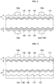
- FIG. 2 is a cross-sectional view of a bifacial solar cell taken along line II-II of FIG. 1 according to one embodiment of the invention.
- FIG. 3 is a cross-sectional view of a mono-facial solar cell taken along line II-II of FIG. 1 according to another embodiment of the invention.
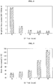
- FIG. 4 is a graph showing a relationship between an oxygen content and a light absorptance of a transparent conductive layer.
- FIG. 5 is a graph showing a relationship between an oxygen content and a sheet resistance of a transparent conductive layer.
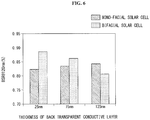
- FIG. 6 is a graph showing a relationship between a thickness of a back transparent conductive layer and reflection characteristic in a mono-facial solar cell and a bifacial solar cell according to embodiments of the invention.
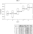
- FIG. 7 is a graph showing a relationship between a thickness of a back transparent conductive layer and an oxygen content and a short circuit current density in a bifacial solar cell according to an embodiment of the invention.
- a solar cell includes a crystalline semiconductor substrate 110.
- a front surface and a back surface of the semiconductor substrate 110 may be formed as a texturing surface including a plurality of fine unevennesses.
- the back surface of the semiconductor substrate 110 may be formed as a substantially flat surface without fine unevennesses.
- a front passivation layer 120, a front doped layer 130, a front transparent conductive layer 140, and a front collector electrode 150 are sequentially stacked on the front surface of the semiconductor substrate 110.
- a back passivation layer 160, a back doped layer 170, a back transparent conductive layer 180, and a back collector electrode 190 are sequentially stacked on the back surface of the semiconductor substrate 110.
- front surface refers to a surface facing upward in the accompanying drawings
- back surface refers to a surface facing downward in the accompanying drawings.
- the substrate 110 is a semiconductor substrate 110 made of crystalline silicon containing impurities of a first conductivity type, for example, an n-type.
- silicon may be single crystal silicon or polycrystalline silicon.
- the substrate 110 contains impurities of a group V element such as phosphorus (P), arsenic (As), antimony (Sb), or the like.
- a group V element such as phosphorus (P), arsenic (As), antimony (Sb), or the like.
- the substrate 110 may be a p-type and may be made of a semiconductor material other than silicon.
- the substrate 110 may contain impurities of a group III element such as boron (B), gallium (Ga), indium (In), or the like.
- the substrate 110 has the n-type.
- the substrate 110 has a texturing surface whose surface is textured. More specifically, the substrate 110 includes both a front surface, on which the front passivation layer 120 is located, and a back surface, on which the back passivation layer 160 is located, as a texturing surface.
- the front passivation layer 120 and the back passivation layer 160 may be formed of substantially intrinsic (i-type) amorphous silicon or may be formed of a tunnel oxide.
- the front passivation layer 120 and the back passivation layer 160 may be formed to have a thickness of approximately 5 nm on substantially the entire area of the front and back surfaces of the substrate 110.
- each of the front passivation layer 120 and the back passivation layer 160 has the same surface shape as the texturing surface of the substrate 110. That is, each of the front passivation layer 120 and the back passivation layer 160 has a texturing surface.
- the front doped layer 130 located on the front passivation layer 120 is an impurity doped region of a second conductive type (for example, a p-type) opposite the conductive type of the substrate 110.
- the front doped layer 130 is formed of p-type amorphous silicon (p-a-Si) and forms a p-n junction and a hetero junction with the substrate 110.
- the substrate 110 has the n-type and the front doped layer 130 has the p-type, the separated electrons move toward the substrate 110 and the separated holes move toward the front doped layer 130.
- the front doped layer 130 has the n-type.
- the separated holes move toward the substrate 110, and the separated electrons move toward the front doped layer 130.
- the front transparent conductive layer 140 formed on the front doped layer 130 may be formed of a layer containing indium oxide (In 2 O 3 ) as a main component and containing tin (Sn), zinc (Zn), tungsten (W), cerium (Ce) or hydrogen (H) as impurities, or a layer containing indium oxide as a main component and containing at least one of titanium (Ti) and tantalum (Ta) as impurities, or a layer containing zinc oxide (ZnO) as a main component and containing aluminum (Al), boron (B), or gallium (Ga) as impurities, or a layer containing tin oxide (SnO 2 ) as a main component and containing fluorine (F) as impurities.
- the front transparent conductive layer 140 has an anti-reflection function for increasing the amount of light incident on the semiconductor substrate 110, and a function to transfer charges moved to the front doped layer 130 to the front collector electrode 150.
- the front transparent conductive layer 140 having the above functions is formed with a first thickness T1 of approximately 70 nm to 100 nm in consideration of anti-reflection characteristics.
- the front doped layer 130 and the front transparent conductive layer 140 are formed to have the same surface shape as the texturing surface of the substrate 110.
- the front collector electrode 150 located on the front transparent conductive layer 140 includes a plurality of finger electrodes 150a extending in a first direction X-X and spaced apart in parallel, and at least one bus bar electrode 150b extending in a second direction Y-Y orthogonal to the first direction X-X and physically connected to the plurality of finger electrodes 150a.
- the front collector electrode 150 is formed of a metal having excellent conductivity, for example, silver (Ag).
- the back doped layer 170 is located under the back passivation layer 160 located on the back surface of the semiconductor substrate 110.
- the back doped layer 170 is an impurity doped region having a first conductivity type (for example, an n-type), which is the same as the conductive type of the substrate 110 and is made of n-type amorphous silicon.
- the back doped layer 170 forms a hetero junction with the substrate 110.
- the semiconductor substrate 110 and the back doped layer 170 have the n-type, the separated electrons move toward the back doped layer 170 and the separated holes move toward the front doped layer 130.
- the back doped layer 170 has the p-type.
- the separated holes move toward the back doped layer 170, and the separated electrons move toward the front doped layer 130.
- the back transparent conductive layer 180 formed under the back doped layer 170, that is, on the back surface thereof, has a back reflect function, and a function to transfer charges moved to the back doped layer 170 to the back collector electrode 190.
- the back transparent conductive layer 180 is formed of the same material as the front transparent conductive layer 140.
- the same material refers to a material having a main component and an impurity identical to each other, and the material having different types of impurities contained therein do not correspond to the same material.
- the front transparent conductive layer 140 is made of In 2 O 3 : W (hereinafter referred to as "IWO"), that is, indium oxide (In 2 O 3 ) as a main component containing tungsten (W) as an impurity, similarly to the front transparent conductive layer 140, the back transparent conductive layer 180 is made of IWO.
- IWO In 2 O 3 : W
- the front transparent conductive layer 140 and the back transparent conductive layer 180 may be formed of different materials.
- Each of the back doped layer 170 and the back transparent conductive layer 180 has the same surface shape as the texturing surface of the substrate 110.
- the back collector electrode 190 is located under the back transparent conductive layer 180, that is, on a lower part thereof.
- the back collector electrode 190 may have the same structure as the front collector electrode 150, that is, a finger electrode and a bus bar electrode 190b. As shown in FIG. 3 , the back collector electrode 190 may include a sheet electrode 190' entirely covering a back surface of the back transparent conductive layer 180.
- the solar cell in which the front collector electrode 150 and the back collector electrode 190 are formed as the same structure can be used as a bifacial solar cell.
- the solar cell in which the front collector electrode 150 and the back collector electrode 190' are formed as different structures can be used as a mono-facial solar cell.
- a region where the front collector electrode 150 is formed becomes a shading region where no light is incident.
- the size (width, etc.) of the front collector electrode 150 in order to reduce a shading loss due to the front collector electrode 150.
- the size of the front collector electrode 150 is reduced, the charges moved toward the front doped layer 130 cannot be effectively collected.
- the front transparent conductive layer 140 it is preferable but not required to consider the electrical characteristics rather than the optical characteristics.
- the back transparent conductive layer 180 it is preferable but not required to further consider the optical characteristics rather than the electrical characteristics.
- the sheet resistance of the front transparent conductive layer 140 is formed to be less than the sheet resistance of the back transparent conductive layer 180
- the light absorptance of the back transparent conductive layer 180 is formed to be less than the light absorptance of the front transparent conductive layer 140.
- FIG. 4 is a graph showing a relationship between oxygen content and light absorptance of a transparent conductive layer IWO.
- FIG. 5 is a graph showing a relationship between oxygen content and sheet resistance of a transparent conductive layer IWO.
- the light absorptance decreases from 350 nm to 1200 nm.
- the light absorptance is greatly reduced when the oxygen is injected in an amount of 15 sccm as compared with the instance of injecting oxygen in an amount of 10 seem.
- the sheet resistance increases.
- the sheet resistance is greatly increased when the amount of oxygen is injected in an amount of 90 seem as compared with the instance of injecting oxygen in an amount of 50 sccm.
- the back transparent conductive layer 180 when the back transparent conductive layer 180 is formed, it is preferable but not required to inject oxygen in an amount of 15 sccm to 50 seem to improve the optical characteristics and electrical characteristics of the back transparent conductive layer 180. It is more preferable but not required to inject oxygen in an amount of 15 seem to 30 sccm.
- the front transparent conductive layer 140 Since it is preferable but not required that the front transparent conductive layer 140 consider the electrical characteristics more than the optical characteristics as compared with the back transparent conductive layer 180, when the front transparent conductive layer 140 is formed, it can be seen that it is preferable but not required to inject oxygen in an amount less than 15 seem, especially less than 10 seem.
- the oxygen content of the front transparent conductive layer 140 is formed to be smaller than the oxygen content of the back transparent conductive layer 180. Accordingly, the sheet resistance of the front transparent conductive layer 140 is formed to be smaller than the sheet resistance of the back transparent conductive layer 180.
- FIG. 6 is a graph showing a relationship between a thickness of a back transparent conductive layer and reflection characteristic in a mono-facial solar cell and a bifacial solar cell.
- the back reflection characteristic BSR @ 1200 nm
- the back reflection characteristic increases as the thickness of the back transparent conductive layer 180 increases.
- the back reflection characteristic increases as the thickness of the back transparent conductive layer 180 decreases.
- a second thickness T2 of the back transparent conductive layer 180 is formed to be less than a first thickness T1 of the front transparent conductive layer 140.
- a second thickness T2 of the back transparent conductive layer 180 is formed to be greater than a first thickness T1 of the front transparent conductive layer 140.
- the second thickness T2 of the back transparent conductive layer 180 is formed within a range less than the first thickness T1 of the front transparent conductive layer 140, in the instance of the mono-facial solar cell shown in FIG. 3 , the second thickness T2 of the back transparent conductive layer 180 is formed within a range larger than the first thickness T1 of the front transparent conductive layer 140.
- FIG. 7 is a graph showing a relationship between a thickness of a back transparent conductive layer, oxygen content, and short circuit current density in a bifacial solar cell.
- split 1 is a sample formed with a thickness of 75 nm while injecting oxygen in an amount of 25 seem.
- Split 2 is a sample formed with a thickness of 50 nm while injecting oxygen in an amount of 25 seem.
- Split 3 is a sample formed with a thickness of 25 nm while injecting oxygen in an amount of 25 seem.
- Split 4 is a sample formed with a thickness of 50 nm while injecting oxygen in an amount of 50 sccm.
- Split 5 is a sample formed with a thickness of 25 nm while injecting oxygen in an amount of 50 sccm.
- the second thickness T2 of the back transparent conductive layer 180 is 25 nm or more, a good short circuit current density Jsc can be obtained.
- the second thickness T2 of the back transparent conductive layer 180 is formed to be 25 nm or more within a range less than the first thickness T1 of the front transparent conductive layer 140.
- the second thickness T2 of the back transparent conductive layer 180 is formed to be 25 nm to 75 nm.
- the second thickness T2 of the back transparent conductive layer 180 increases, the back reflection characteristic increases.
- the second thickness T2 is thickened.
- the second thickness T2 is preferably but not necessarily 500 nm or less considering the material cost of the back transparent conductive layer 180 and bowing of the substrate.
- the second thickness T2 of the back transparent conductive layer 180 may be formed to be 70 nm to 500 nm within a range larger than the first thickness T1 of the front transparent conductive layer 140.
- the above-described solar cells (bifacial type and mono-facial type) can be manufactured as a solar cell module by a modularization process.
- the solar cell module can be manufactured by carrying out a lamination process by positioning a plurality of solar cells electrically connected with adjacent solar cells by an interconnector or a ribbon between a pair of substrates, and by placing a sealing material between both substrates.
- the n-type single crystal silicon substrate is cleaned to remove impurities, and etching is performed using an etching solution composed of an aqueous solution of sodium hydroxide.
- a semiconductor substrate 110 having texturing surfaces formed on front and back surfaces of the silicon substrate is prepared.
- a front passivation layer 120 made of i-type amorphous silicon and a front doped layer 130 made of p-type amorphous silicon are sequentially formed on the front surface of the substrate 110, and a back passivation layer 160 made of i-type amorphous silicon and a back doped layer 170 made of n-type amorphous silicon are sequentially formed on the back surface of the substrate 110.
- RF Radio-frequency
- CVD Radio-frequency
- a front transparent conductive layer 140 is formed on the front doped layer 130.
- the layer material source a sintered body of indium oxide powder containing a predetermined amount of tungsten powder for doping the impurity can be used.
- a back transparent conductive layer 180 is formed under the back doped layer 170, that is, on the back surface of the back doped layer 170.
- the back transparent conductive layer 180 is formed of the same material as the front transparent conductive layer 140.
- the back transparent conductive layer 180 is formed of the same material as the front transparent conductive layer 140.
- oxygen is injected in an amount of less than 15 sccm, especially less than 10 seem.
- oxygen is injected in an amount of 15 sccm to 50 seem, preferably but not necessarily in an amount of 15 sccm to 30 seem.
- the front transparent conductive layer 140 is formed with a first thickness T1 of 70 nm to 100 nm.
- the back transparent conductive layer 180 is formed with a second thickness T2 of 25 nm to 75 nm within a range less than the first thickness T1 of the front transparent conductive layer 140.
- the back transparent conductive layer 180 is formed with a second thickness T2 of 70 nm to 500 nm within a range larger than the first thickness T1 of the front transparent conductive layer 140.
- the back transparent conductive layer 180 may be formed of a different material from the front transparent conductive layer 140.
- An annealing process may be performed for a predetermined time at a predetermined temperature for crystallizing the front transparent conductive layer 140 and the back transparent conductive layer 180 formed by the manufacturing method described above.
- a silver (Ag) paste formed by kneading a silver (Ag) powder into a thermosetting resin such as an epoxy resin is formed into a predetermined shape.
- a thermosetting resin such as an epoxy resin
- a silver paste may be formed on the finger electrode region and the bus bar electrode region on the front transparent conductive layer 140 and the back transparent conductive layer 180.
- the back collector electrode 190 may be formed by applying and curing a conductive paste as a whole on the back transparent conductive layer 180.
Landscapes
- Photovoltaic Devices (AREA)
- Life Sciences & Earth Sciences (AREA)
- Engineering & Computer Science (AREA)
- Sustainable Development (AREA)
- Sustainable Energy (AREA)
Applications Claiming Priority (2)
| Application Number | Priority Date | Filing Date | Title |
|---|---|---|---|
| KR1020160004964A KR101821394B1 (ko) | 2016-01-14 | 2016-01-14 | 태양전지 |
| EP17151397.1A EP3193375B1 (fr) | 2016-01-14 | 2017-01-13 | Cellule solaire |
Related Parent Applications (2)
| Application Number | Title | Priority Date | Filing Date |
|---|---|---|---|
| EP17151397.1A Division EP3193375B1 (fr) | 2016-01-14 | 2017-01-13 | Cellule solaire |
| EP17151397.1A Division-Into EP3193375B1 (fr) | 2016-01-14 | 2017-01-13 | Cellule solaire |
Publications (2)
| Publication Number | Publication Date |
|---|---|
| EP3324447A1 true EP3324447A1 (fr) | 2018-05-23 |
| EP3324447B1 EP3324447B1 (fr) | 2019-03-06 |
Family
ID=57796247
Family Applications (2)
| Application Number | Title | Priority Date | Filing Date |
|---|---|---|---|
| EP17151397.1A Active EP3193375B1 (fr) | 2016-01-14 | 2017-01-13 | Cellule solaire |
| EP17210606.4A Active EP3324447B1 (fr) | 2016-01-14 | 2017-01-13 | Cellule solaire |
Family Applications Before (1)
| Application Number | Title | Priority Date | Filing Date |
|---|---|---|---|
| EP17151397.1A Active EP3193375B1 (fr) | 2016-01-14 | 2017-01-13 | Cellule solaire |
Country Status (5)
| Country | Link |
|---|---|
| US (1) | US20170207354A1 (fr) |
| EP (2) | EP3193375B1 (fr) |
| JP (2) | JP2017126750A (fr) |
| KR (1) | KR101821394B1 (fr) |
| CN (1) | CN107039542B (fr) |
Families Citing this family (16)
| Publication number | Priority date | Publication date | Assignee | Title |
|---|---|---|---|---|
| JP6976101B2 (ja) * | 2017-08-09 | 2021-12-08 | 株式会社カネカ | 結晶シリコン系太陽電池 |
| WO2019054239A1 (fr) * | 2017-09-15 | 2019-03-21 | ソーラーフロンティア株式会社 | Module de conversion photoélectrique et procédé de fabrication de module de conversion photoélectrique |
| WO2019182243A1 (fr) * | 2018-03-19 | 2019-09-26 | 엘지전자 주식회사 | Cellule solaire et son procédé de fabrication |
| CN111223958B (zh) | 2018-11-23 | 2022-10-14 | 成都晔凡科技有限公司 | 叠瓦电池片和叠瓦光伏组件的制造方法和系统 |
| WO2021030235A2 (fr) | 2019-08-09 | 2021-02-18 | Leading Edge Equipment Technologies, Inc. | Tranche comportant des régions à faible concentration en oxygène |
| MX2022001458A (es) | 2019-08-09 | 2022-06-08 | Leading Edge Equipment Tech Inc | Produccion de una cinta u oblea con regiones de baja concentracion de oxigeno. |
| IT202000012613A1 (it) * | 2020-05-27 | 2021-11-27 | 3Sun S R L | Cella solare e modulo di celle solari |
| CN112366232B (zh) * | 2020-10-21 | 2022-12-02 | 长沙壹纳光电材料有限公司 | 一种异质结太阳能电池及其制备方法与应用 |
| CN112768549B (zh) * | 2021-02-09 | 2025-06-10 | 通威太阳能(成都)有限公司 | 一种高光电转换效率的hjt电池及其制备方法 |
| CN117038744A (zh) * | 2021-09-06 | 2023-11-10 | 上海晶科绿能企业管理有限公司 | 太阳能电池及光伏组件 |
| CN114122154B (zh) * | 2021-10-11 | 2023-12-19 | 中国科学院电工研究所 | 一种载流子选择性钝化接触太阳电池及其制备方法 |
| CN115274875B (zh) | 2022-05-31 | 2025-03-18 | 浙江晶科能源有限公司 | 太阳能电池及光伏组件 |
| CN115763588A (zh) * | 2022-11-28 | 2023-03-07 | 福建金石能源有限公司 | 一种p型微晶硅发射极的背抛光异质结电池的制造方法 |
| CN117317040A (zh) * | 2023-09-05 | 2023-12-29 | 天合光能股份有限公司 | 太阳能电池及其制备方法 |
| CN120091656A (zh) * | 2023-10-27 | 2025-06-03 | 安徽华晟新能源科技股份有限公司 | 太阳能电池及其制备方法 |
| US12597878B1 (en) * | 2024-06-30 | 2026-04-07 | United States Of America As Represented By The Secretary Of The Air Force | Albedo collecting solar array |
Citations (2)
| Publication number | Priority date | Publication date | Assignee | Title |
|---|---|---|---|---|
| US20090211627A1 (en) * | 2008-02-25 | 2009-08-27 | Suniva, Inc. | Solar cell having crystalline silicon p-n homojunction and amorphous silicon heterojunctions for surface passivation |
| EP2672522A1 (fr) * | 2011-01-31 | 2013-12-11 | Sanyo Electric Co., Ltd. | Élément de conversion photoélectrique |
Family Cites Families (28)
| Publication number | Priority date | Publication date | Assignee | Title |
|---|---|---|---|---|
| JPS61141185A (ja) * | 1984-12-13 | 1986-06-28 | Fuji Electric Co Ltd | 光起電力素子の製造方法 |
| US5078803A (en) * | 1989-09-22 | 1992-01-07 | Siemens Solar Industries L.P. | Solar cells incorporating transparent electrodes comprising hazy zinc oxide |
| JP3469729B2 (ja) * | 1996-10-31 | 2003-11-25 | 三洋電機株式会社 | 太陽電池素子 |
| JP4197863B2 (ja) * | 2001-09-27 | 2008-12-17 | 三洋電機株式会社 | 光起電力装置の製造方法 |
| JP2003142709A (ja) * | 2001-10-31 | 2003-05-16 | Sharp Corp | 積層型太陽電池およびその製造方法 |
| JP4152197B2 (ja) * | 2003-01-16 | 2008-09-17 | 三洋電機株式会社 | 光起電力装置 |
| JP4162516B2 (ja) * | 2003-03-14 | 2008-10-08 | 三洋電機株式会社 | 光起電力装置 |
| JP5121203B2 (ja) * | 2006-09-29 | 2013-01-16 | 三洋電機株式会社 | 太陽電池モジュール |
| WO2008117605A1 (fr) * | 2007-03-23 | 2008-10-02 | Hamamatsu Foundation For Science And Technology Promotion | Film électroconducteur transparent d'air à grande superficie et son procédé de fabrication |
| US20110056552A1 (en) * | 2008-03-19 | 2011-03-10 | Sanyo Electric Co., Ltd. | Solar cell and method for manufacturing the same |
| KR101146736B1 (ko) * | 2009-09-14 | 2012-05-17 | 엘지전자 주식회사 | 태양 전지 |
| TWI553666B (zh) * | 2009-09-17 | 2016-10-11 | 松下知識產權經營股份有限公司 | 透明導電膜及具備該導電膜之裝置 |
| KR101656118B1 (ko) * | 2009-09-18 | 2016-09-08 | 파나소닉 아이피 매니지먼트 가부시키가이샤 | 태양 전지, 태양 전지 모듈 및 태양 전지 시스템 |
| JP5257372B2 (ja) * | 2009-11-30 | 2013-08-07 | 住友金属鉱山株式会社 | 酸化物蒸着材と透明導電膜および太陽電池 |
| CN102102187A (zh) * | 2009-12-17 | 2011-06-22 | 中环股份有限公司 | 制造具结晶结构的透明导电薄膜的方法 |
| US9059349B2 (en) * | 2010-02-09 | 2015-06-16 | Dow Global Technologies Llc | Moisture resistant photovoltaic devices with improved adhesion of barrier film |
| JP5593917B2 (ja) * | 2010-07-26 | 2014-09-24 | ミツミ電機株式会社 | リセット回路及びそれを備える装置 |
| WO2012020682A1 (fr) * | 2010-08-09 | 2012-02-16 | 株式会社カネカ | Cellule solaire au silicium cristallin |
| US9123861B2 (en) * | 2011-12-21 | 2015-09-01 | Mitsubishi Electric Corporation | Solar battery, manufacturing method thereof, and solar battery module |
| EP2669952B1 (fr) * | 2012-06-01 | 2015-03-25 | Roth & Rau AG | Dispositif photovoltaïque et son procédé de fabrication |
| WO2014002249A1 (fr) * | 2012-06-29 | 2014-01-03 | 三洋電機株式会社 | Cellule solaire, module de cellules solaires et procédé de production de cellule solaire |
| MY168566A (en) * | 2012-10-02 | 2018-11-13 | Kaneka Corp | Method for manufacturing crystalline silicon solar cell, method for manufacturing solar cell module, crystalline silicon solar cell, and solar cell module |
| CN103227246A (zh) * | 2013-04-11 | 2013-07-31 | 浙江正泰太阳能科技有限公司 | 一种异质结电池的制备方法 |
| JP2015073058A (ja) * | 2013-10-04 | 2015-04-16 | 長州産業株式会社 | 光発電素子 |
| JP2015119008A (ja) * | 2013-12-17 | 2015-06-25 | 株式会社カネカ | 太陽電池モジュールおよびその製造方法 |
| KR20150144585A (ko) * | 2014-06-17 | 2015-12-28 | 엘지전자 주식회사 | 태양 전지의 후처리 장치 |
| KR102290310B1 (ko) * | 2014-11-14 | 2021-08-13 | 삼성전자주식회사 | 전도성 박막 |
| US9947822B2 (en) * | 2015-02-02 | 2018-04-17 | Tesla, Inc. | Bifacial photovoltaic module using heterojunction solar cells |
-
2016
- 2016-01-14 KR KR1020160004964A patent/KR101821394B1/ko active Active
-
2017
- 2017-01-11 CN CN201710017356.XA patent/CN107039542B/zh active Active
- 2017-01-13 JP JP2017004207A patent/JP2017126750A/ja active Pending
- 2017-01-13 EP EP17151397.1A patent/EP3193375B1/fr active Active
- 2017-01-13 EP EP17210606.4A patent/EP3324447B1/fr active Active
- 2017-01-13 US US15/406,345 patent/US20170207354A1/en not_active Abandoned
-
2018
- 2018-12-12 JP JP2018232696A patent/JP2019041131A/ja active Pending
Patent Citations (2)
| Publication number | Priority date | Publication date | Assignee | Title |
|---|---|---|---|---|
| US20090211627A1 (en) * | 2008-02-25 | 2009-08-27 | Suniva, Inc. | Solar cell having crystalline silicon p-n homojunction and amorphous silicon heterojunctions for surface passivation |
| EP2672522A1 (fr) * | 2011-01-31 | 2013-12-11 | Sanyo Electric Co., Ltd. | Élément de conversion photoélectrique |
Also Published As
| Publication number | Publication date |
|---|---|
| CN107039542B (zh) | 2019-12-24 |
| EP3324447B1 (fr) | 2019-03-06 |
| JP2017126750A (ja) | 2017-07-20 |
| JP2019041131A (ja) | 2019-03-14 |
| EP3193375B1 (fr) | 2018-05-09 |
| KR20170085389A (ko) | 2017-07-24 |
| KR101821394B1 (ko) | 2018-01-23 |
| CN107039542A (zh) | 2017-08-11 |
| US20170207354A1 (en) | 2017-07-20 |
| EP3193375A1 (fr) | 2017-07-19 |
Similar Documents
| Publication | Publication Date | Title |
|---|---|---|
| EP3193375B1 (fr) | Cellule solaire | |
| EP3196945B1 (fr) | Cellule solaire | |
| US20240421238A1 (en) | Solar cell | |
| US11056598B2 (en) | Solar cell | |
| EP2219222B1 (fr) | Cellule solaire et son procédé de fabrication | |
| US9508875B2 (en) | Solar cell and method for manufacturing the same | |
| KR101918738B1 (ko) | 태양 전지 | |
| JP7185818B2 (ja) | 太陽電池及びその製造方法 | |
| US20190088802A1 (en) | Moisture-resistant solar cells for solar roof tiles | |
| EP4318601B1 (fr) | Cellule solaire et procédé de fabrication de cellule solaire | |
| US12622089B2 (en) | Solar cell | |
| US20240063314A1 (en) | A solar cell | |
| GB2636587A (en) | Photovoltaic device |
Legal Events
| Date | Code | Title | Description |
|---|---|---|---|
| PUAI | Public reference made under article 153(3) epc to a published international application that has entered the european phase |
Free format text: ORIGINAL CODE: 0009012 |
|
| STAA | Information on the status of an ep patent application or granted ep patent |
Free format text: STATUS: THE APPLICATION HAS BEEN PUBLISHED |
|
| AC | Divisional application: reference to earlier application |
Ref document number: 3193375 Country of ref document: EP Kind code of ref document: P |
|
| AK | Designated contracting states |
Kind code of ref document: A1 Designated state(s): AL AT BE BG CH CY CZ DE DK EE ES FI FR GB GR HR HU IE IS IT LI LT LU LV MC MK MT NL NO PL PT RO RS SE SI SK SM TR |
|
| AX | Request for extension of the european patent |
Extension state: BA ME |
|
| STAA | Information on the status of an ep patent application or granted ep patent |
Free format text: STATUS: REQUEST FOR EXAMINATION WAS MADE |
|
| GRAP | Despatch of communication of intention to grant a patent |
Free format text: ORIGINAL CODE: EPIDOSNIGR1 |
|
| STAA | Information on the status of an ep patent application or granted ep patent |
Free format text: STATUS: GRANT OF PATENT IS INTENDED |
|
| 17P | Request for examination filed |
Effective date: 20180813 |
|
| RBV | Designated contracting states (corrected) |
Designated state(s): AL AT BE BG CH CY CZ DE DK EE ES FI FR GB GR HR HU IE IS IT LI LT LU LV MC MK MT NL NO PL PT RO RS SE SI SK SM TR |
|
| RIC1 | Information provided on ipc code assigned before grant |
Ipc: H01L 31/0224 20060101AFI20180830BHEP Ipc: H01L 31/0236 20060101ALI20180830BHEP Ipc: H01L 31/0747 20120101ALI20180830BHEP Ipc: H01L 31/0216 20140101ALI20180830BHEP |
|
| RIC1 | Information provided on ipc code assigned before grant |
Ipc: H01L 31/0224 20060101AFI20180831BHEP Ipc: H01L 31/0747 20120101ALI20180831BHEP Ipc: H01L 31/0236 20060101ALI20180831BHEP Ipc: H01L 31/18 20060101ALI20180831BHEP Ipc: H01L 31/0216 20140101ALI20180831BHEP |
|
| INTG | Intention to grant announced |
Effective date: 20180919 |
|
| GRAS | Grant fee paid |
Free format text: ORIGINAL CODE: EPIDOSNIGR3 |
|
| GRAA | (expected) grant |
Free format text: ORIGINAL CODE: 0009210 |
|
| STAA | Information on the status of an ep patent application or granted ep patent |
Free format text: STATUS: THE PATENT HAS BEEN GRANTED |
|
| AC | Divisional application: reference to earlier application |
Ref document number: 3193375 Country of ref document: EP Kind code of ref document: P |
|
| AK | Designated contracting states |
Kind code of ref document: B1 Designated state(s): AL AT BE BG CH CY CZ DE DK EE ES FI FR GB GR HR HU IE IS IT LI LT LU LV MC MK MT NL NO PL PT RO RS SE SI SK SM TR |
|
| REG | Reference to a national code |
Ref country code: GB Ref legal event code: FG4D |
|
| REG | Reference to a national code |
Ref country code: AT Ref legal event code: REF Ref document number: 1105716 Country of ref document: AT Kind code of ref document: T Effective date: 20190315 Ref country code: CH Ref legal event code: EP |
|
| REG | Reference to a national code |
Ref country code: IE Ref legal event code: FG4D |
|
| REG | Reference to a national code |
Ref country code: DE Ref legal event code: R096 Ref document number: 602017002543 Country of ref document: DE |
|
| REG | Reference to a national code |
Ref country code: NL Ref legal event code: FP |
|
| REG | Reference to a national code |
Ref country code: LT Ref legal event code: MG4D |
|
| PG25 | Lapsed in a contracting state [announced via postgrant information from national office to epo] |
Ref country code: LT Free format text: LAPSE BECAUSE OF FAILURE TO SUBMIT A TRANSLATION OF THE DESCRIPTION OR TO PAY THE FEE WITHIN THE PRESCRIBED TIME-LIMIT Effective date: 20190306 Ref country code: SE Free format text: LAPSE BECAUSE OF FAILURE TO SUBMIT A TRANSLATION OF THE DESCRIPTION OR TO PAY THE FEE WITHIN THE PRESCRIBED TIME-LIMIT Effective date: 20190306 Ref country code: NO Free format text: LAPSE BECAUSE OF FAILURE TO SUBMIT A TRANSLATION OF THE DESCRIPTION OR TO PAY THE FEE WITHIN THE PRESCRIBED TIME-LIMIT Effective date: 20190606 Ref country code: FI Free format text: LAPSE BECAUSE OF FAILURE TO SUBMIT A TRANSLATION OF THE DESCRIPTION OR TO PAY THE FEE WITHIN THE PRESCRIBED TIME-LIMIT Effective date: 20190306 |
|
| PG25 | Lapsed in a contracting state [announced via postgrant information from national office to epo] |
Ref country code: BG Free format text: LAPSE BECAUSE OF FAILURE TO SUBMIT A TRANSLATION OF THE DESCRIPTION OR TO PAY THE FEE WITHIN THE PRESCRIBED TIME-LIMIT Effective date: 20190606 Ref country code: RS Free format text: LAPSE BECAUSE OF FAILURE TO SUBMIT A TRANSLATION OF THE DESCRIPTION OR TO PAY THE FEE WITHIN THE PRESCRIBED TIME-LIMIT Effective date: 20190306 Ref country code: HR Free format text: LAPSE BECAUSE OF FAILURE TO SUBMIT A TRANSLATION OF THE DESCRIPTION OR TO PAY THE FEE WITHIN THE PRESCRIBED TIME-LIMIT Effective date: 20190306 Ref country code: GR Free format text: LAPSE BECAUSE OF FAILURE TO SUBMIT A TRANSLATION OF THE DESCRIPTION OR TO PAY THE FEE WITHIN THE PRESCRIBED TIME-LIMIT Effective date: 20190607 Ref country code: LV Free format text: LAPSE BECAUSE OF FAILURE TO SUBMIT A TRANSLATION OF THE DESCRIPTION OR TO PAY THE FEE WITHIN THE PRESCRIBED TIME-LIMIT Effective date: 20190306 |
|
| REG | Reference to a national code |
Ref country code: AT Ref legal event code: MK05 Ref document number: 1105716 Country of ref document: AT Kind code of ref document: T Effective date: 20190306 |
|
| PG25 | Lapsed in a contracting state [announced via postgrant information from national office to epo] |
Ref country code: SK Free format text: LAPSE BECAUSE OF FAILURE TO SUBMIT A TRANSLATION OF THE DESCRIPTION OR TO PAY THE FEE WITHIN THE PRESCRIBED TIME-LIMIT Effective date: 20190306 Ref country code: AL Free format text: LAPSE BECAUSE OF FAILURE TO SUBMIT A TRANSLATION OF THE DESCRIPTION OR TO PAY THE FEE WITHIN THE PRESCRIBED TIME-LIMIT Effective date: 20190306 Ref country code: PT Free format text: LAPSE BECAUSE OF FAILURE TO SUBMIT A TRANSLATION OF THE DESCRIPTION OR TO PAY THE FEE WITHIN THE PRESCRIBED TIME-LIMIT Effective date: 20190706 Ref country code: EE Free format text: LAPSE BECAUSE OF FAILURE TO SUBMIT A TRANSLATION OF THE DESCRIPTION OR TO PAY THE FEE WITHIN THE PRESCRIBED TIME-LIMIT Effective date: 20190306 Ref country code: RO Free format text: LAPSE BECAUSE OF FAILURE TO SUBMIT A TRANSLATION OF THE DESCRIPTION OR TO PAY THE FEE WITHIN THE PRESCRIBED TIME-LIMIT Effective date: 20190306 Ref country code: ES Free format text: LAPSE BECAUSE OF FAILURE TO SUBMIT A TRANSLATION OF THE DESCRIPTION OR TO PAY THE FEE WITHIN THE PRESCRIBED TIME-LIMIT Effective date: 20190306 Ref country code: IT Free format text: LAPSE BECAUSE OF FAILURE TO SUBMIT A TRANSLATION OF THE DESCRIPTION OR TO PAY THE FEE WITHIN THE PRESCRIBED TIME-LIMIT Effective date: 20190306 Ref country code: CZ Free format text: LAPSE BECAUSE OF FAILURE TO SUBMIT A TRANSLATION OF THE DESCRIPTION OR TO PAY THE FEE WITHIN THE PRESCRIBED TIME-LIMIT Effective date: 20190306 |
|
| PG25 | Lapsed in a contracting state [announced via postgrant information from national office to epo] |
Ref country code: SM Free format text: LAPSE BECAUSE OF FAILURE TO SUBMIT A TRANSLATION OF THE DESCRIPTION OR TO PAY THE FEE WITHIN THE PRESCRIBED TIME-LIMIT Effective date: 20190306 Ref country code: PL Free format text: LAPSE BECAUSE OF FAILURE TO SUBMIT A TRANSLATION OF THE DESCRIPTION OR TO PAY THE FEE WITHIN THE PRESCRIBED TIME-LIMIT Effective date: 20190306 |
|
| REG | Reference to a national code |
Ref country code: DE Ref legal event code: R097 Ref document number: 602017002543 Country of ref document: DE |
|
| PG25 | Lapsed in a contracting state [announced via postgrant information from national office to epo] |
Ref country code: IS Free format text: LAPSE BECAUSE OF FAILURE TO SUBMIT A TRANSLATION OF THE DESCRIPTION OR TO PAY THE FEE WITHIN THE PRESCRIBED TIME-LIMIT Effective date: 20190706 Ref country code: AT Free format text: LAPSE BECAUSE OF FAILURE TO SUBMIT A TRANSLATION OF THE DESCRIPTION OR TO PAY THE FEE WITHIN THE PRESCRIBED TIME-LIMIT Effective date: 20190306 |
|
| PLBE | No opposition filed within time limit |
Free format text: ORIGINAL CODE: 0009261 |
|
| STAA | Information on the status of an ep patent application or granted ep patent |
Free format text: STATUS: NO OPPOSITION FILED WITHIN TIME LIMIT |
|
| PG25 | Lapsed in a contracting state [announced via postgrant information from national office to epo] |
Ref country code: DK Free format text: LAPSE BECAUSE OF FAILURE TO SUBMIT A TRANSLATION OF THE DESCRIPTION OR TO PAY THE FEE WITHIN THE PRESCRIBED TIME-LIMIT Effective date: 20190306 |
|
| 26N | No opposition filed |
Effective date: 20191209 |
|
| PG25 | Lapsed in a contracting state [announced via postgrant information from national office to epo] |
Ref country code: TR Free format text: LAPSE BECAUSE OF FAILURE TO SUBMIT A TRANSLATION OF THE DESCRIPTION OR TO PAY THE FEE WITHIN THE PRESCRIBED TIME-LIMIT Effective date: 20190306 |
|
| PG25 | Lapsed in a contracting state [announced via postgrant information from national office to epo] |
Ref country code: MC Free format text: LAPSE BECAUSE OF FAILURE TO SUBMIT A TRANSLATION OF THE DESCRIPTION OR TO PAY THE FEE WITHIN THE PRESCRIBED TIME-LIMIT Effective date: 20190306 |
|
| REG | Reference to a national code |
Ref country code: CH Ref legal event code: PL |
|
| REG | Reference to a national code |
Ref country code: NL Ref legal event code: MM Effective date: 20200201 |
|
| REG | Reference to a national code |
Ref country code: BE Ref legal event code: MM Effective date: 20200131 |
|
| PG25 | Lapsed in a contracting state [announced via postgrant information from national office to epo] |
Ref country code: LU Free format text: LAPSE BECAUSE OF NON-PAYMENT OF DUE FEES Effective date: 20200113 Ref country code: FR Free format text: LAPSE BECAUSE OF NON-PAYMENT OF DUE FEES Effective date: 20200131 Ref country code: NL Free format text: LAPSE BECAUSE OF NON-PAYMENT OF DUE FEES Effective date: 20200201 |
|
| PG25 | Lapsed in a contracting state [announced via postgrant information from national office to epo] |
Ref country code: LI Free format text: LAPSE BECAUSE OF NON-PAYMENT OF DUE FEES Effective date: 20200131 Ref country code: CH Free format text: LAPSE BECAUSE OF NON-PAYMENT OF DUE FEES Effective date: 20200131 Ref country code: BE Free format text: LAPSE BECAUSE OF NON-PAYMENT OF DUE FEES Effective date: 20200131 |
|
| PG25 | Lapsed in a contracting state [announced via postgrant information from national office to epo] |
Ref country code: IE Free format text: LAPSE BECAUSE OF NON-PAYMENT OF DUE FEES Effective date: 20200113 |
|
| GBPC | Gb: european patent ceased through non-payment of renewal fee |
Effective date: 20210113 |
|
| PG25 | Lapsed in a contracting state [announced via postgrant information from national office to epo] |
Ref country code: GB Free format text: LAPSE BECAUSE OF NON-PAYMENT OF DUE FEES Effective date: 20210113 |
|
| PG25 | Lapsed in a contracting state [announced via postgrant information from national office to epo] |
Ref country code: MT Free format text: LAPSE BECAUSE OF FAILURE TO SUBMIT A TRANSLATION OF THE DESCRIPTION OR TO PAY THE FEE WITHIN THE PRESCRIBED TIME-LIMIT Effective date: 20190306 Ref country code: CY Free format text: LAPSE BECAUSE OF FAILURE TO SUBMIT A TRANSLATION OF THE DESCRIPTION OR TO PAY THE FEE WITHIN THE PRESCRIBED TIME-LIMIT Effective date: 20190306 |
|
| PG25 | Lapsed in a contracting state [announced via postgrant information from national office to epo] |
Ref country code: MK Free format text: LAPSE BECAUSE OF FAILURE TO SUBMIT A TRANSLATION OF THE DESCRIPTION OR TO PAY THE FEE WITHIN THE PRESCRIBED TIME-LIMIT Effective date: 20190306 |
|
| REG | Reference to a national code |
Ref country code: DE Ref legal event code: R081 Ref document number: 602017002543 Country of ref document: DE Owner name: SHANGRAO JINKO SOLAR TECHNOLOGY DEVELOPMENT CO, CN Free format text: FORMER OWNER: LG ELECTRONICS INC., SEOUL, KR Ref country code: DE Ref legal event code: R082 Ref document number: 602017002543 Country of ref document: DE Representative=s name: DREISS PATENTANWAELTE PARTG MBB, DE Ref country code: DE Ref legal event code: R082 Ref document number: 602017002543 Country of ref document: DE Representative=s name: MANITZ FINSTERWALD PATENT- UND RECHTSANWALTSPA, DE Ref country code: DE Ref legal event code: R081 Ref document number: 602017002543 Country of ref document: DE Owner name: TRINA SOLAR CO., LTD., CHANGZHOU, CN Free format text: FORMER OWNER: LG ELECTRONICS INC., SEOUL, KR Ref country code: DE Ref legal event code: R081 Ref document number: 602017002543 Country of ref document: DE Owner name: SHANGRAO XINYUAN YUEDONG TECHNOLOGY DEVELOPMEN, CN Free format text: FORMER OWNER: LG ELECTRONICS INC., SEOUL, KR |
|
| PG25 | Lapsed in a contracting state [announced via postgrant information from national office to epo] |
Ref country code: SI Free format text: LAPSE BECAUSE OF FAILURE TO SUBMIT A TRANSLATION OF THE DESCRIPTION OR TO PAY THE FEE WITHIN THE PRESCRIBED TIME-LIMIT Effective date: 20190306 |
|
| REG | Reference to a national code |
Ref country code: DE Ref legal event code: R081 Ref document number: 602017002543 Country of ref document: DE Owner name: TRINA SOLAR CO., LTD., CHANGZHOU, CN Free format text: FORMER OWNER: SHANGRAO JINKO SOLAR TECHNOLOGY DEVELOPMENT CO., LTD, SHANGRAO, JIANGXI PROVINCE, CN Ref country code: DE Ref legal event code: R081 Ref document number: 602017002543 Country of ref document: DE Owner name: SHANGRAO XINYUAN YUEDONG TECHNOLOGY DEVELOPMEN, CN Free format text: FORMER OWNER: SHANGRAO JINKO SOLAR TECHNOLOGY DEVELOPMENT CO., LTD, SHANGRAO, JIANGXI PROVINCE, CN |
|
| REG | Reference to a national code |
Ref country code: DE Ref legal event code: R082 Ref document number: 602017002543 Country of ref document: DE Representative=s name: MANITZ FINSTERWALD PATENT- UND RECHTSANWALTSPA, DE Ref country code: DE Ref legal event code: R081 Ref document number: 602017002543 Country of ref document: DE Owner name: TRINA SOLAR CO., LTD., CHANGZHOU, CN Free format text: FORMER OWNER: SHANGRAO XINYUAN YUEDONG TECHNOLOGY DEVELOPMENT CO. LTD, SHANGRAO, JIANGXI PROVINCE, CN |
|
| REG | Reference to a national code |
Ref country code: DE Ref legal event code: R079 Ref document number: 602017002543 Country of ref document: DE Free format text: PREVIOUS MAIN CLASS: H01L0031022400 Ipc: H10F0077200000 |
|
| PGFP | Annual fee paid to national office [announced via postgrant information from national office to epo] |
Ref country code: DE Payment date: 20260120 Year of fee payment: 10 |