EP3325313B1 - Miroir plein affichage - Google Patents
Miroir plein affichage Download PDFInfo
- Publication number
- EP3325313B1 EP3325313B1 EP16852462.7A EP16852462A EP3325313B1 EP 3325313 B1 EP3325313 B1 EP 3325313B1 EP 16852462 A EP16852462 A EP 16852462A EP 3325313 B1 EP3325313 B1 EP 3325313B1
- Authority
- EP
- European Patent Office
- Prior art keywords
- electro
- optic element
- optic
- mirror assembly
- electrical connection
- Prior art date
- Legal status (The legal status is an assumption and is not a legal conclusion. Google has not performed a legal analysis and makes no representation as to the accuracy of the status listed.)
- Active
Links
Images


Classifications
-
- B—PERFORMING OPERATIONS; TRANSPORTING
- B60—VEHICLES IN GENERAL
- B60R—VEHICLES, VEHICLE FITTINGS, OR VEHICLE PARTS, NOT OTHERWISE PROVIDED FOR
- B60R1/00—Optical viewing arrangements; Real-time viewing arrangements for drivers or passengers using optical image capturing systems, e.g. cameras or video systems specially adapted for use in or on vehicles
- B60R1/02—Rear-view mirror arrangements
- B60R1/08—Rear-view mirror arrangements involving special optical features, e.g. avoiding blind spots, e.g. convex mirrors; Side-by-side associations of rear-view and other mirrors
- B60R1/083—Anti-glare mirrors, e.g. "day-night" mirrors
- B60R1/088—Anti-glare mirrors, e.g. "day-night" mirrors using a cell of electrically changeable optical characteristic, e.g. liquid-crystal or electrochromic mirrors
-
- B—PERFORMING OPERATIONS; TRANSPORTING
- B60—VEHICLES IN GENERAL
- B60R—VEHICLES, VEHICLE FITTINGS, OR VEHICLE PARTS, NOT OTHERWISE PROVIDED FOR
- B60R1/00—Optical viewing arrangements; Real-time viewing arrangements for drivers or passengers using optical image capturing systems, e.g. cameras or video systems specially adapted for use in or on vehicles
- B60R1/12—Mirror assemblies combined with other articles, e.g. clocks
-
- G—PHYSICS
- G02—OPTICS
- G02F—OPTICAL DEVICES OR ARRANGEMENTS FOR THE CONTROL OF LIGHT BY MODIFICATION OF THE OPTICAL PROPERTIES OF THE MEDIA OF THE ELEMENTS INVOLVED THEREIN; NON-LINEAR OPTICS; FREQUENCY-CHANGING OF LIGHT; OPTICAL LOGIC ELEMENTS; OPTICAL ANALOGUE/DIGITAL CONVERTERS
- G02F1/00—Devices or arrangements for the control of the intensity, colour, phase, polarisation or direction of light arriving from an independent light source, e.g. switching, gating or modulating; Non-linear optics
- G02F1/01—Devices or arrangements for the control of the intensity, colour, phase, polarisation or direction of light arriving from an independent light source, e.g. switching, gating or modulating; Non-linear optics for the control of the intensity, phase, polarisation or colour
- G02F1/15—Devices or arrangements for the control of the intensity, colour, phase, polarisation or direction of light arriving from an independent light source, e.g. switching, gating or modulating; Non-linear optics for the control of the intensity, phase, polarisation or colour based on an electrochromic effect
- G02F1/153—Constructional details
- G02F1/155—Electrodes
-
- G—PHYSICS
- G02—OPTICS
- G02F—OPTICAL DEVICES OR ARRANGEMENTS FOR THE CONTROL OF LIGHT BY MODIFICATION OF THE OPTICAL PROPERTIES OF THE MEDIA OF THE ELEMENTS INVOLVED THEREIN; NON-LINEAR OPTICS; FREQUENCY-CHANGING OF LIGHT; OPTICAL LOGIC ELEMENTS; OPTICAL ANALOGUE/DIGITAL CONVERTERS
- G02F1/00—Devices or arrangements for the control of the intensity, colour, phase, polarisation or direction of light arriving from an independent light source, e.g. switching, gating or modulating; Non-linear optics
- G02F1/01—Devices or arrangements for the control of the intensity, colour, phase, polarisation or direction of light arriving from an independent light source, e.g. switching, gating or modulating; Non-linear optics for the control of the intensity, phase, polarisation or colour
- G02F1/15—Devices or arrangements for the control of the intensity, colour, phase, polarisation or direction of light arriving from an independent light source, e.g. switching, gating or modulating; Non-linear optics for the control of the intensity, phase, polarisation or colour based on an electrochromic effect
- G02F1/153—Constructional details
- G02F1/157—Structural association of cells with optical devices, e.g. reflectors or illuminating devices
-
- G—PHYSICS
- G02—OPTICS
- G02F—OPTICAL DEVICES OR ARRANGEMENTS FOR THE CONTROL OF LIGHT BY MODIFICATION OF THE OPTICAL PROPERTIES OF THE MEDIA OF THE ELEMENTS INVOLVED THEREIN; NON-LINEAR OPTICS; FREQUENCY-CHANGING OF LIGHT; OPTICAL LOGIC ELEMENTS; OPTICAL ANALOGUE/DIGITAL CONVERTERS
- G02F1/00—Devices or arrangements for the control of the intensity, colour, phase, polarisation or direction of light arriving from an independent light source, e.g. switching, gating or modulating; Non-linear optics
- G02F1/01—Devices or arrangements for the control of the intensity, colour, phase, polarisation or direction of light arriving from an independent light source, e.g. switching, gating or modulating; Non-linear optics for the control of the intensity, phase, polarisation or colour
- G02F1/15—Devices or arrangements for the control of the intensity, colour, phase, polarisation or direction of light arriving from an independent light source, e.g. switching, gating or modulating; Non-linear optics for the control of the intensity, phase, polarisation or colour based on an electrochromic effect
- G02F1/153—Constructional details
- G02F1/161—Gaskets; Spacers; Sealing of cells; Filling or closing of cells
-
- B—PERFORMING OPERATIONS; TRANSPORTING
- B60—VEHICLES IN GENERAL
- B60R—VEHICLES, VEHICLE FITTINGS, OR VEHICLE PARTS, NOT OTHERWISE PROVIDED FOR
- B60R1/00—Optical viewing arrangements; Real-time viewing arrangements for drivers or passengers using optical image capturing systems, e.g. cameras or video systems specially adapted for use in or on vehicles
- B60R1/12—Mirror assemblies combined with other articles, e.g. clocks
- B60R2001/1215—Mirror assemblies combined with other articles, e.g. clocks with information displays
-
- G—PHYSICS
- G02—OPTICS
- G02F—OPTICAL DEVICES OR ARRANGEMENTS FOR THE CONTROL OF LIGHT BY MODIFICATION OF THE OPTICAL PROPERTIES OF THE MEDIA OF THE ELEMENTS INVOLVED THEREIN; NON-LINEAR OPTICS; FREQUENCY-CHANGING OF LIGHT; OPTICAL LOGIC ELEMENTS; OPTICAL ANALOGUE/DIGITAL CONVERTERS
- G02F1/00—Devices or arrangements for the control of the intensity, colour, phase, polarisation or direction of light arriving from an independent light source, e.g. switching, gating or modulating; Non-linear optics
- G02F1/01—Devices or arrangements for the control of the intensity, colour, phase, polarisation or direction of light arriving from an independent light source, e.g. switching, gating or modulating; Non-linear optics for the control of the intensity, phase, polarisation or colour
- G02F1/15—Devices or arrangements for the control of the intensity, colour, phase, polarisation or direction of light arriving from an independent light source, e.g. switching, gating or modulating; Non-linear optics for the control of the intensity, phase, polarisation or colour based on an electrochromic effect
- G02F1/153—Constructional details
- G02F1/155—Electrodes
- G02F2001/1557—Side by side arrangements of working and counter electrodes
-
- G—PHYSICS
- G02—OPTICS
- G02F—OPTICAL DEVICES OR ARRANGEMENTS FOR THE CONTROL OF LIGHT BY MODIFICATION OF THE OPTICAL PROPERTIES OF THE MEDIA OF THE ELEMENTS INVOLVED THEREIN; NON-LINEAR OPTICS; FREQUENCY-CHANGING OF LIGHT; OPTICAL LOGIC ELEMENTS; OPTICAL ANALOGUE/DIGITAL CONVERTERS
- G02F2203/00—Function characteristic
- G02F2203/02—Function characteristic reflective
Definitions
- the present disclosure generally relates to vehicle mirror systems, and more specifically, to rearview mirror systems.
- Vehicles typically include a rearview mirror system to allow a driver of the vehicle to observe behind the vehicle.
- Incorporation of display elements into rear view mirror assemblies may present dimensional constraint issues related to placement of electrical components such as connections and conductors.
- a display mirror assembly for a vehicle includes a full display module and an electro-optic element including a plurality of sides defined at a periphery of the electro-optic element.
- the electro-optic element includes a first substantially transparent substrate having first and second surfaces disposed on opposite sides thereof.
- the second surface includes a first electrically conductive layer.
- a second substantially transparent substrate has third and fourth surfaces disposed on opposite sides thereof.
- the third surface includes a second electrically conductive layer.
- a primary seal is disposed between the first and second substrates. The seal and the first and second substrates define a cavity therebetween.
- An electro-optic medium is disposed in the cavity.
- the electro-optic medium is variably transmissive such that the electro-optic medium is operable between generally clear and darkened states.
- a first electrical connection and a second electrical connection are positioned on the same side of the electro-optic element.
- a display mirror assembly for a vehicle includes a full display module and an electro-optic element that includes a first substantially transparent substrate having first and second surfaces disposed on opposite sides thereof and a second substantially transparent substrate having third and fourth surfaces disposed on opposite sides thereof.
- a primary seal is disposed between the first and second substrates.
- a first conductor is positioned along a top of the electro-optic element between the first and second substrates and electrically coupled to a first electrical connection.
- a second conductor is positioned between the first and second substrates with the second conductor electrically coupled to a second electrical connection and an electrically conductive layer. The second conductor is electrically coupled to the second electrical connection on a different side of the electro-optic element than the electrically conductive layer.
- a display mirror assembly for a vehicle includes a full display module and an electro-optic element positioned vehicle forward of the full display module.
- the electro-optic element includes a first substantially transparent substrate, a second substantially transparent substrate, an electro-optic medium positioned between the first and second substrates, and a first electrical connection and a second electrical connection positioned on a same side of the electro-optic element.
- a first conductor is electrically coupled with the first electrical connection and a second conductor is electrically coupled to the second electrical connection.
- the first conductor and the second conductor are electrically coupled with the electro-optic medium on opposite sides of the electro-optic element.
- a display mirror which offers increased flexibility in design, decreased component size, increased aesthetic appeal to a viewer, and uniform transitioning of an electro-optic medium between a clear and darkened state regardless of where electricity coupled to the display mirror.
- EP 0 434 453 A2 which is direct to an electro-optic mirror, having a perimeter coating applied to a front or rear surface of a substrate element for concealing seals and/or electrical connections but does not disclose any form of display module as set forth in the present application.
- the terms "upper,” “lower,” “right,” “left,” “rear,” “front,” “vertical,” “horizontal,” and derivatives thereof shall relate to the disclosure as oriented in FIG. 1 .
- the disclosure may assume various alternative orientations, except where expressly specified to the contrary.
- the specific devices and processes illustrated in the attached drawings, and described in the following specification are simply exemplary embodiments of the inventive concepts defined in the appended claims. Hence, specific dimensions and other physical characteristics relating to the embodiments disclosed herein are not to be considered as limiting unless the claims expressly state otherwise.
- reference numeral 10 generally designates a display mirror assembly for a vehicle including a full display module 12 and an electro-optic element 14.
- the electro-optic element 14 includes a plurality of sides defined at a periphery of the electro-optic element 14.
- the electro-optic element 14 includes a first substantially transparent substrate 16 having a first surface 18 and a second surface 22 disposed on opposite sides thereof.
- the second surface 22 includes a first electrically conductive layer 26.
- a second substantially transparent substrate 30 includes a third surface 34 and a fourth surface 38 disposed on opposite sides thereof.
- the third surface 34 includes a second electrically conductive layer 42.
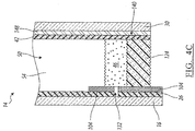
- a primary seal 46 is disposed between the first and second substrates 16, 30, wherein the seal 46 and the first and second substrates 16, 30 define a cavity 50 therebetween.
- An electro-optic medium 54 is disposed in the cavity 50.
- the electro-optic medium 54 is variably transmissive such that the electro-optic element 14 is operable between generally clear and darkened states.
- a first electrical connection 58 and a second electrical connection 62 are positioned on a same side of the electro-optic element 14.
- the electro-optic element 14, as described and depicted herein, may include a plurality of sides. Sides of the electro-optic element 14 may be longitudinal extents, either curved or substantially linear, which are separated by corners (e.g., abrupt changes of direction greater than about 10°). For example, a rectangular shape of the electro-optic element 14 (as depicted), includes four sides (i.e., top, bottom, and two sides), however electro-optic elements 14 having an oval shape (e.g., two sides), round shape (e.g., one side), or shapes with greater than four sides (e.g., pentagon) are considered.
- the display mirror assembly 10 has a viewing area 80, which includes the first surface 18 of the electro-optic element 14.
- the viewing area 80 may be a rectangular shape, a trapezoidal shape, or any custom contoured shape desired for aesthetic reasons.
- the display mirror assembly 10 may be mounted to a vehicle via a mounting member 84 extending rearwardly from the display mirror assembly 10.
- the display mirror assembly 10 for a vehicle is shown, with the components partially exploded.
- the display mirror assembly 10 includes the electro-optic element 14, a front shield 88 and a rear shield 92 encapsulating the full display module 12, a rear housing 96, and the mounting member 84.
- the full display module 12 may be manufactured similarly to that described in U.S. Patent Application Publication No. 2014/0268355 A1 , which is herein incorporated by reference in its entirety.
- a "full" display module 12 is a module where the display module 12 is at least about 70%, at least about 75%, at least about 80%, at least about 85%, at least about 90%, at least about 95% or at least about 99% of the total display surface of the display mirror assembly 10.
- the front shield 88, the rear shield 92, and components of the full display module 12 include various retaining features to operably connect the several components of the full display module 12 with the front shield 88, the rear shield 92 and each other, and to provide support to the full display module 12.
- the front shield 88 includes retaining features to operably connect the front shield 88 to the full display module 12, and the rear shield 92 has retaining features to operably connect the rear shield 92 to the full display module 12.
- the retaining features may include snap-fit connections, tab and slot connections, screw connections, and other known retaining features. Some or all of the retaining features may also be strengthened by the addition of adhesive compounds.
- the electro-optic element 14 is generally planar, with an outer perimeter 100 and a spectral filter 104 around the outer perimeter 100.
- the spectral filter 104 may incorporate a hiding layer such as a chrome ring or other similar finish to conceal the front shield 88 and other elements located within and/or behind the electro-optic element 14 in the display mirror assembly 10, including, without limitation, the primary seal 46 on an electrochromic unit, an applique, foam adhesive, pad printing, etc.
- the spectral filter 104 may extend from the outer perimeter 100 of the electro-optic element 14 to an outer edge 108 of the full display module 12.
- the spectral filter 104 may be narrower and not reach from the outer perimeter 100 to the outer edge 108 of the full display module 12 along at least some portions of the spectral filter 104.
- the perimeter of the first substrate 16 of the electro-optic element 14 may also have a ground edge, a beveled edge, a seamed edge, a laser cut edge, or combinations thereof.
- the front shield 88 functions to shield the full display module 12 from radio frequency (RF) electromagnetic radiation and to provide support for the electro-optic element 14 and the full display module 12.
- the front shield 88 is formed from one or more materials which are suitable to block RF radiation including, without limitation, steel.
- the front shield 88 can be formed from a stamped steel material which may be about 0.2 mm thick.
- the full display module 12 is disposed behind the front shield 88, with a display screen 112 viewable through an opening in the front shield 88.
- the display module 12 may be LCD, LED, OLED, plasma, DLP or other display technology. Further, the display module 12 may incorporate one or more light guides.
- the second substrate 30 is slightly smaller than the first substrate 16 which results in a relatively small offset between the first and second substrates 16, 30.
- Such an embodiment may be advantageous in concealing the first and second electrical connections 58, 62 as well as for providing a distinct edge to the electro-optic element 14.
- the first and second electrical connections 58, 62 may be an electrical clip, such as a J-clip, or include multiple electrical connection components such as a male to female connection.
- the primary seal 46 traverses an approximate perimeter of, and is configured to, cooperate with the first and second substrates 16, 30 to define the cavity 50 between the first and second substrate 16, 30.
- the cavity 50 may be substantially hermetic.
- the primary seal 46 may be applied to the first or second substrates 16, 30 by methods commonly used in the liquid crystal display (LCD) industry, such as by silk-screening or dispensing.
- the spectral filter 104 extends inboard from the primary seal 46 into the cavity 50 sufficiently far enough to generally conceal the primary seal 46 from the viewer.
- the electro-optic medium 54 is disposed within the cavity 50.
- the electro-optic element 14 may be an electrochromic element.
- the electro-optic medium 54 may be an electrochromic medium, which includes at least one solvent, at least one anodic material, and at least one cathodic material.
- both of the anodic and cathodic materials are electroactive and at least one of them is electrochromic.
- electrochromic will be defined herein as a material that undergoes a modification in its oxidation state upon exposure to a particular electrical potential difference.
- Electrochromic components include materials whose color or opacity are affected by electric current, such that when an electrical field is applied to the material, the color or opacity changes from a first phase to a second phase.
- the electrochromic component may be a single-layer, single-phase component, multi-layer component, or multi-phase component, as described in U.S. Patent Nos.
- a first conductor 120 and a second conductor 124 are disposed around a portion of a perimeter of the electro-optic element 14.
- the first and second conductors 120, 124 are positioned outboard of the primary seal 46 and serve to electrically connect the first electrical connection 58 to the first electrically conductive layer 26 and the second electrical connection 62 to the second electrically conductive layer 42.
- the first and second electrically conductive layers 26, 42 may be formed of indium tin-oxide, aluminum-doped zinc-oxide and indium-doped cadmium-oxide, carbon nanotubes, graphene, or combinations thereof.
- the second electrically conductive layer 42 may include a metal reflector or one or more coatings configured as any of the partially reflective, partially transmissive ("transflective") coatings disclosed in U.S. Patent No. 6,700,692 , the entire disclosure of which is incorporated herein by reference.
- the first and second conductors 120, 124 may be a conductive solder, a conductive epoxy (e.g., silver epoxy), a wire, metal solder, ultrasonic solder, conductive ink, conductive frit and/or other material capable of electrical transfer.
- the first and second conductors 120, 124 are different materials.
- the first conductor 120 extends along a top perimeter of the electro-optic element 14, on both sides of the first electrical connection 58, but in other embodiments may only extend from a single side of the first electrical connection 58.
- the first conductor 120 is electrically coupled with the spectral filter 104 which provides electrical connection to the first electrically conductive layer 26.
- Positioned between the first conductor 120 and the second electrical connection 62 is an isolation gap 128. At the isolation gap 128, the thickness of the primary seal 46 expands and functions to prevent a short in the path of electricity through the electro-optic element 14.
- the isolation gap 128 may have a length of greater than about 0.1 cm, greater than about 0.5 cm, greater than about 1.0 cm, greater than about 1.5 cm, greater than about 2.0 cm, greater than about 2.5 cm, greater than about 3.0 cm, greater than about 3.5 cm or greater than about 4 cm. Alternatively, the isolation gap 128 may have a length of less than about 30 mm.
- the second conductor 124 is in electrical communication with the second electrical connection 62.
- the second conductor 124 begins at the second electrical connection 62 and extends along a side and bottom of the electro-optic element 14.
- an isolation line 132 is disposed through the first electrically conductive layer 26 and the spectral filter 104.
- the isolation line 132 is configured to electrically separate the second conductor 124 from the first electrically conductive layer 26.
- the isolation line 132 is depicted as disposed over the primary seal 46, but may be positioned in a variety of locations that electrically separate the second conductor 124 from the first electrically conductive layer 26.
- the isolation line 132 may be formed via laser ablation of the spectral filter 104 and first electrically conductive layer 26 or may be formed via selective application of the spectral filter 104 and first electrically conductive layer 26.
- the isolation line 132 may have a thickness of less than about 40 ⁇ , less than about 30 ⁇ , less than about 20 ⁇ , less than about 15 ⁇ , less than about 14 ⁇ , less than about 13 ⁇ , less than about 12 ⁇ , less than about 11 ⁇ , less than about 10 ⁇ , less than about 9 ⁇ , less than about 8 ⁇ , less than about 7 ⁇ , less than about 6 ⁇ or less than about 5 ⁇ .
- the isolation line 132 may be of a sufficiently small width that the isolation line 132 is not perceptible to the human eye. In other embodiments, the isolation line 132 may extend around the electro-optic element 14 such that the isolation line 132 has aesthetically pleasing reflection symmetry across the electro-optic element 14.
- Portions of the second electrically conductive layer 42 and a film 148 positioned on the third surface 34 may be continuously ablated along the perimeter of the electro-optic element 14 and ablated at a bottom side of the electro-optic element 14 to form a "saw tooth" pattern.
- the conductive layer 42 and the film 148 define a plurality of openings 136 and a multitude of contacts 140.
- the ablated perimeter of the electro-optic element 14 and the plurality of openings 136 allow the primary seal 46, the first conductor 120 and/or the second conductor 124 to be viewed and inspected for defects (e.g., gaps or holes).
- the contacts 140 extend over the primary seal 46 toward the second conductor 124.
- the contacts 140 are electrically coupled to the second conductor 124, thereby facilitating electrical coupling between the second conductor 124 and the second electrically conductive layer 42.
- Use of the ablation and contacts 140 allows for a largely uniform application of electricity to the electro-optic medium 54 which facilitates an even transition between clear and darkened states of the electro-optic medium 54 in electrochromic embodiments of the electro-optic element 14.
- the largely uniform application of electricity to the electro-optic medium 54 facilitates the even transition between the clear and darkened states by ensuring that portions of the electro-optic medium 54 do not darken faster than other portions.
- the electro-optic element 14 may include the film 148 positioned on the third surface 34.
- the film 148 may be reflective, transmissive, or may have a combination of partially reflective and partially transmissive properties.
- use of the film 148 may allow a viewer of the display mirror assembly 10 to view the full display module 12 ( FIG. 2 ) while it is active (e.g., emitting light), but also perceive the film 148 as a reflective mirror while the full display module 12 is off (e.g., not emitting light) due to the reflective properties of the film 148.
- first and second conductors 120, 124 on the same side, the isolation line 132, and the conductive bus 1366 allows a variety of advantages to be realized.
- use of the disclosed first and second conductors 120, 124 may allow designers of the electro-optic element 14 to decouple where electricity enters the electro-optic element 14 from where the electricity enters the electro-optic medium 54.
- electrical connections must be placed on opposite sides of the element in order to achieve a uniform change across the element.
- This disclosure is advantageous in that it may allow use of a smaller bezel, frame or housing around the electro-optic element 14 due to optimum placement of the first and second electrical connections 58, 62, while still channeling electricity to the electro-optic medium 54 in a way that facilitates even transitioning of the electro-optic medium 54 between clear and darkened states.
- use of the first and second conductors 120, 124 allow for flexibility in the design of the display mirror assembly 10 by allowing the movement of the first and second electrical connections 58, 62 to areas proximate less moveable connections.
- the full display module 12 may have a display connector protruding from a top of the full display module 12.
- the first and second conductors 120, 124 may be utilized so that all electrical connections (e.g., the display connector for the full display module 12 and the first and second electrical connections 58, 62) are positioned on a single side (e.g., the top side) of the display mirror assembly 10, thereby allowing a thinner profile elsewhere around the display mirror assembly 10. Additionally, use of the first and second conductors 120, 124 may allow for a radio frequency shield (e.g., front shield 88 and rear shield 92) and/or allow fewer or smaller openings to be made through the shield.
- a radio frequency shield e.g., front shield 88 and rear shield 92
- first and second conductors 120, 124 may be positioned in a variety of locations around the electro-optic element 14.
- the first and second electrical connections 58, 62 may be located on a side of the electro-optic element 14 (e.g., on each side of a fill port) with the first and second conductors 120, 124 extending in opposite directions along sides of the electro-optic element 14.
- the present disclosure may be used with a rearview assembly such as that described in U.S. Patent Nos. 8,925,891 ; 8,814,373 ; 8,201,800 ; and 8,210,695 ; U.S. Patent Application Publication Nos. 2014/0063630 and 2012/0327234 ; and U.S. Provisional Patent Application Nos. 61/709,716 ; 61/707,676 ; and 61/704,869 , which are hereby incorporated herein by reference in their entirety. Further, the present disclosure may be used with a rearview packaging assembly such as that described in U.S. Patent Nos.
- Coupled in all of its forms: couple, coupling, coupled, etc. generally means the joining of two components (electrical or mechanical) directly or indirectly to one another. Such joining may be stationary in nature or movable in nature. Such joining may be achieved with the two components, electrical or mechanical, and any additional intermediate members being integrally formed as a single unitary body with one another or with the two components. Such joining may be permanent in nature, or may be removable or releasable in nature, unless otherwise stated.
- elements shown as integrally formed may be constructed of multiple parts, or elements shown as multiple parts may be integrally formed, the operation of the interfaces may be reversed or otherwise varied, the length or width of the structures and/or members or connector or other elements of the system may be varied, the nature or number of adjustment positions provided between the elements may be varied.
- the elements and/or assemblies of the system may be constructed from any of a wide variety of materials that provide sufficient strength or durability, in any of a wide variety of colors, textures, and combinations. Accordingly, all such modifications are intended to be included within the scope of the present innovations. Other substitutions, modifications, changes, and omissions may be made in the design, operating conditions, and arrangement of the desired and other exemplary embodiments.
Landscapes
- Physics & Mathematics (AREA)
- Nonlinear Science (AREA)
- Engineering & Computer Science (AREA)
- General Physics & Mathematics (AREA)
- Optics & Photonics (AREA)
- Multimedia (AREA)
- Mechanical Engineering (AREA)
- Chemical & Material Sciences (AREA)
- Crystallography & Structural Chemistry (AREA)
- Electrochromic Elements, Electrophoresis, Or Variable Reflection Or Absorption Elements (AREA)
- Fittings On The Vehicle Exterior For Carrying Loads, And Devices For Holding Or Mounting Articles (AREA)
Claims (6)
- Un ensemble miroir à afficheur (10) pour un véhicule, comprenant :un module plein affichage (12) ; etun élément électro-optique (14) incluant une pluralité de côtés définis à une périphérie de l'élément électro-optique (14), l'élément électro-optique (14) comprenant :un premier substrat sensiblement transparent (16) ayant des surfaces première et deuxième (18, 22) disposées sur ses côtés opposés, sachant que la deuxième surface (22) comprend une première couche électriquement conductrice (26) ;un deuxième substrat sensiblement transparent (30) ayant des surfaces troisième et quatrième (34, 38) disposées sur ses côtés opposés, sachant que la troisième surface (34) comprend une deuxième couche électriquement conductrice (42) ;un élément d'étanchéité primaire (46) disposé entre les substrats premier et deuxième (16, 30), sachant que l'élément d'étanchéité (46) et les substrats premier et deuxième (16, 30) définissent une cavité (50) entre eux;un milieu électro-optique (54) disposé dans la cavité (50), le milieu électro-optique (54) étant variablement transmissif de manière que le milieu électro-optique (54) soit fonctionnel entre des états sensiblement clairs et sombres ; etune première connexion électrique (58) et une deuxième connexion électrique (62), sachant que les connexions électriques première et deuxième (58, 62) sont positionnées du même côté de l'élément électro-optique (14).
- L'ensemble miroir à afficheur (10) d'après la revendication 1, sachant que l'élément électro-optique (14) est partiellement transmissif et partiellement réfléchissant.
- L'ensemble miroir à afficheur (10) d'après l'une des revendications 1 et 2, sachant que le module plein affichage (12) est positionné relativement à la direction du véhicule devant l'élément électro-optique (14).
- L'ensemble miroir à afficheur (10) d'après l'une quelconque des revendications de 1 à 3, sachant que la première connexion électrique (58) est couplée électriquement avec un premier conducteur (120) et que la deuxième connexion électrique (62) est couplée électriquement avec un deuxième conducteur (124).
- L'ensemble miroir à afficheur (10) d'après la revendication 4, sachant que le deuxième conducteur (124) s'étend vers un côté opposé de l'élément électro-optique (14) à la première connexion électrique (58).
- L'ensemble miroir à afficheur (10) d'après la revendication 5, sachant que les conducteurs premier et deuxième (120, 124) sont positionnés en dehors de l'élément d'étanchéité primaire (46).
Applications Claiming Priority (2)
| Application Number | Priority Date | Filing Date | Title |
|---|---|---|---|
| US201562235156P | 2015-09-30 | 2015-09-30 | |
| PCT/US2016/054128 WO2017058882A1 (fr) | 2015-09-30 | 2016-09-28 | Rétroviseur complet |
Publications (3)
| Publication Number | Publication Date |
|---|---|
| EP3325313A1 EP3325313A1 (fr) | 2018-05-30 |
| EP3325313A4 EP3325313A4 (fr) | 2019-01-02 |
| EP3325313B1 true EP3325313B1 (fr) | 2020-02-12 |
Family
ID=58408434
Family Applications (1)
| Application Number | Title | Priority Date | Filing Date |
|---|---|---|---|
| EP16852462.7A Active EP3325313B1 (fr) | 2015-09-30 | 2016-09-28 | Miroir plein affichage |
Country Status (6)
| Country | Link |
|---|---|
| US (1) | US10179546B2 (fr) |
| EP (1) | EP3325313B1 (fr) |
| JP (1) | JP6720297B2 (fr) |
| KR (1) | KR102077074B1 (fr) |
| CN (1) | CN108136962B (fr) |
| WO (1) | WO2017058882A1 (fr) |
Families Citing this family (9)
| Publication number | Priority date | Publication date | Assignee | Title |
|---|---|---|---|---|
| US10442360B2 (en) | 2017-03-02 | 2019-10-15 | Magna Mirrors Of America, Inc. | Interior rearview mirror assembly with display and tilt mechanism |
| US11110864B2 (en) | 2017-08-23 | 2021-09-07 | Magna Mirrors Of America, Inc. | Interior rearview mirror assembly with full screen video display |
| US11214199B2 (en) | 2019-06-03 | 2022-01-04 | Magna Mirrors Of America, Inc. | Interior rearview mirror assembly with display and tilt mechanism |
| CN114041084B (zh) * | 2019-07-25 | 2024-06-25 | 金泰克斯公司 | 分段可变受控电光元件 |
| US11932170B2 (en) * | 2019-10-21 | 2024-03-19 | Gentex Corporation | Switchable mirror and display |
| CN111025809A (zh) * | 2019-11-18 | 2020-04-17 | 爱卓智能科技(上海)有限公司 | 电致变色后视镜中方便灌注电致变色液的方法 |
| US12145507B2 (en) | 2020-04-20 | 2024-11-19 | Magna Mirrors Of America, Inc. | Interior rearview mirror assembly with actuator |
| US20230347825A1 (en) * | 2022-04-29 | 2023-11-02 | Aimcore Technology Co., Ltd. | Electrochromic rearview mirror assembly with large viewable reflective region |
| KR102751394B1 (ko) | 2023-03-27 | 2025-01-08 | (주)마팔하이테코 | 전기변색미러 및 디스플레이 결합된 확장형 디바이스 |
Family Cites Families (39)
| Publication number | Priority date | Publication date | Assignee | Title |
|---|---|---|---|---|
| US3280701A (en) | 1961-09-05 | 1966-10-25 | Donnelly Mirrors Inc | Optically variable one-way mirror |
| SE370754B (fr) | 1971-10-29 | 1974-10-28 | Emmaboda Glasverk Ab | |
| US4902108A (en) | 1986-03-31 | 1990-02-20 | Gentex Corporation | Single-compartment, self-erasing, solution-phase electrochromic devices, solutions for use therein, and uses thereof |
| DE3736075A1 (de) | 1987-10-24 | 1989-05-03 | Schott Glaswerke | Elektrochromes schichtenpaket |
| US5115346A (en) | 1988-02-12 | 1992-05-19 | Donnelly Corporation | Anti-scatter, ultraviolet protected, anti-misting, electro-optical rearview mirror |
| US5073012A (en) | 1988-02-12 | 1991-12-17 | Donnelly Corporation | Anti-scatter, ultraviolet protected, anti-misting, electro-optical assemblies |
| US5052163A (en) | 1989-11-27 | 1991-10-01 | Georgia Doors & Plywood Service, Inc. | Framed panel assembly |
| US5066112A (en) | 1989-12-21 | 1991-11-19 | Donnelly Corporation | Perimeter coated, electro-optic mirror |
| US5076673A (en) | 1990-08-10 | 1991-12-31 | Donnelly Corporation | Prolonged coloration electrochromic assembly |
| US5253109A (en) | 1992-04-27 | 1993-10-12 | Donnelly Corporation | Electro-optic device with constant light transmitting area |
| FR2690536B1 (fr) | 1992-04-28 | 1994-06-17 | Saint Gobain Vitrage Int | Vitrage electrochrome. |
| US5790298A (en) | 1994-05-03 | 1998-08-04 | Gentex Corporation | Method of forming optically transparent seal and seal formed by said method |
| US5668663A (en) * | 1994-05-05 | 1997-09-16 | Donnelly Corporation | Electrochromic mirrors and devices |
| JP3061543B2 (ja) | 1994-12-29 | 2000-07-10 | 株式会社村上開明堂 | Ec素子を有した室外鏡 |
| US5818625A (en) | 1997-04-02 | 1998-10-06 | Gentex Corporation | Electrochromic rearview mirror incorporating a third surface metal reflector |
| DE19737978C2 (de) | 1997-08-30 | 1999-09-16 | Bayer Ag | Elektrochromer Spiegel |
| US6317248B1 (en) | 1998-07-02 | 2001-11-13 | Donnelly Corporation | Busbars for electrically powered cells |
| US6102546A (en) | 1999-04-01 | 2000-08-15 | Gentex Corporation | Rearview mirror bezel having reduced apparent size |
| US6350843B1 (en) | 1999-06-02 | 2002-02-26 | Hsu San Fa | Epoxy resin low electronic impedance high molecular polymer |
| US7064882B2 (en) | 2002-09-30 | 2006-06-20 | Gentex Corporation | Electrochromic devices having no positional offset between substrates |
| WO2001084230A1 (fr) * | 2000-05-04 | 2001-11-08 | Schott Donnelly Llc | Vitrage chromogene |
| US6407847B1 (en) | 2000-07-25 | 2002-06-18 | Gentex Corporation | Electrochromic medium having a color stability |
| EP1437620A1 (fr) * | 2001-10-05 | 2004-07-14 | Murakami Corporation | Element electrochimique de type liquide |
| US20060061008A1 (en) * | 2004-09-14 | 2006-03-23 | Lee Karner | Mounting assembly for vehicle interior mirror |
| US7184190B2 (en) * | 2002-09-20 | 2007-02-27 | Donnelly Corporation | Electro-optic reflective element assembly |
| US7310177B2 (en) * | 2002-09-20 | 2007-12-18 | Donnelly Corporation | Electro-optic reflective element assembly |
| US7446924B2 (en) * | 2003-10-02 | 2008-11-04 | Donnelly Corporation | Mirror reflective element assembly including electronic component |
| CN201383065Y (zh) * | 2009-04-09 | 2010-01-13 | 宁波市金榜汽车电子有限公司 | 一种电致变色器件 |
| US8964278B2 (en) * | 2010-08-09 | 2015-02-24 | Gentex Corporation | Electro-optic system configured to reduce a perceived color change |
| CN201926848U (zh) * | 2010-12-15 | 2011-08-10 | 比亚迪股份有限公司 | 一种防眩后视镜 |
| DE102011013132A1 (de) * | 2011-03-04 | 2012-09-06 | Thüringisches Institut für Textil- und Kunststoff-Forschung e.V. | Stabiles elektrochromes Modul |
| JP5612003B2 (ja) * | 2012-03-03 | 2014-10-22 | 株式会社ホンダロック | エレクトロクロミックミラー |
| CN202815955U (zh) * | 2012-08-28 | 2013-03-20 | 广东铁将军防盗设备有限公司 | 后视镜行车记录仪 |
| CN103909868B (zh) * | 2013-01-04 | 2016-04-06 | 常州雅谱智能变色光学器件有限公司 | 车辆前视智能防眩光装置及其防眩光镜的制造方法 |
| CN105074544A (zh) * | 2013-03-15 | 2015-11-18 | 金泰克斯公司 | 显示镜组件 |
| TW201621437A (zh) * | 2014-12-10 | 2016-06-16 | Tintable Kibing Co Ltd | 電致變色裝置 |
| US9878669B2 (en) * | 2015-02-24 | 2018-01-30 | Magna Mirrors Of America, Inc. | Mirror assembly with spring-loaded electrical connectors |
| CN104834146B (zh) * | 2015-05-25 | 2018-05-01 | 京东方科技集团股份有限公司 | 一种显示器件、其制作方法、其驱动方法及显示装置 |
| US10421404B2 (en) * | 2015-06-26 | 2019-09-24 | Magna Mirrors Of America, Inc. | Interior rearview mirror assembly with full screen video display |
-
2016
- 2016-09-28 CN CN201680056899.6A patent/CN108136962B/zh active Active
- 2016-09-28 KR KR1020187009439A patent/KR102077074B1/ko active Active
- 2016-09-28 WO PCT/US2016/054128 patent/WO2017058882A1/fr not_active Ceased
- 2016-09-28 US US15/278,709 patent/US10179546B2/en active Active
- 2016-09-28 JP JP2018516732A patent/JP6720297B2/ja active Active
- 2016-09-28 EP EP16852462.7A patent/EP3325313B1/fr active Active
Non-Patent Citations (1)
| Title |
|---|
| None * |
Also Published As
| Publication number | Publication date |
|---|---|
| EP3325313A1 (fr) | 2018-05-30 |
| JP2018535870A (ja) | 2018-12-06 |
| CN108136962A (zh) | 2018-06-08 |
| JP6720297B2 (ja) | 2020-07-08 |
| KR102077074B1 (ko) | 2020-02-13 |
| CN108136962B (zh) | 2021-06-29 |
| WO2017058882A1 (fr) | 2017-04-06 |
| US10179546B2 (en) | 2019-01-15 |
| KR20180049009A (ko) | 2018-05-10 |
| US20170088055A1 (en) | 2017-03-30 |
| EP3325313A4 (fr) | 2019-01-02 |
Similar Documents
| Publication | Publication Date | Title |
|---|---|---|
| EP3325313B1 (fr) | Miroir plein affichage | |
| EP2841303B1 (fr) | Ensemble rétroviseur à afficheur | |
| AU2014326772B2 (en) | Display mirror assembly | |
| US9598018B2 (en) | Display mirror assembly | |
| JP6553186B2 (ja) | ディスプレイミラーアセンブリ | |
| WO2017087476A1 (fr) | Barrière de gaz électro-optique | |
| CN109952232B (zh) | 用于电光元件的电连接 | |
| US9488892B2 (en) | Printed appliqué and method thereof | |
| CN108349436B (zh) | 后视装置 | |
| CN221039483U (zh) | 一种汽车外后视镜镜片的镀膜层结构 | |
| JP2007223369A (ja) | 防眩ミラー |
Legal Events
| Date | Code | Title | Description |
|---|---|---|---|
| STAA | Information on the status of an ep patent application or granted ep patent |
Free format text: STATUS: THE INTERNATIONAL PUBLICATION HAS BEEN MADE |
|
| PUAI | Public reference made under article 153(3) epc to a published international application that has entered the european phase |
Free format text: ORIGINAL CODE: 0009012 |
|
| STAA | Information on the status of an ep patent application or granted ep patent |
Free format text: STATUS: REQUEST FOR EXAMINATION WAS MADE |
|
| 17P | Request for examination filed |
Effective date: 20180223 |
|
| AK | Designated contracting states |
Kind code of ref document: A1 Designated state(s): AL AT BE BG CH CY CZ DE DK EE ES FI FR GB GR HR HU IE IS IT LI LT LU LV MC MK MT NL NO PL PT RO RS SE SI SK SM TR |
|
| AX | Request for extension of the european patent |
Extension state: BA ME |
|
| A4 | Supplementary search report drawn up and despatched |
Effective date: 20181203 |
|
| RIC1 | Information provided on ipc code assigned before grant |
Ipc: B60R 1/04 20060101AFI20181127BHEP Ipc: G02F 1/15 20060101ALI20181127BHEP Ipc: B60R 1/08 20060101ALI20181127BHEP |
|
| DAV | Request for validation of the european patent (deleted) | ||
| DAX | Request for extension of the european patent (deleted) | ||
| GRAP | Despatch of communication of intention to grant a patent |
Free format text: ORIGINAL CODE: EPIDOSNIGR1 |
|
| STAA | Information on the status of an ep patent application or granted ep patent |
Free format text: STATUS: GRANT OF PATENT IS INTENDED |
|
| INTG | Intention to grant announced |
Effective date: 20190911 |
|
| GRAS | Grant fee paid |
Free format text: ORIGINAL CODE: EPIDOSNIGR3 |
|
| GRAA | (expected) grant |
Free format text: ORIGINAL CODE: 0009210 |
|
| STAA | Information on the status of an ep patent application or granted ep patent |
Free format text: STATUS: THE PATENT HAS BEEN GRANTED |
|
| AK | Designated contracting states |
Kind code of ref document: B1 Designated state(s): AL AT BE BG CH CY CZ DE DK EE ES FI FR GB GR HR HU IE IS IT LI LT LU LV MC MK MT NL NO PL PT RO RS SE SI SK SM TR |
|
| REG | Reference to a national code |
Ref country code: GB Ref legal event code: FG4D |
|
| REG | Reference to a national code |
Ref country code: CH Ref legal event code: EP |
|
| REG | Reference to a national code |
Ref country code: AT Ref legal event code: REF Ref document number: 1231675 Country of ref document: AT Kind code of ref document: T Effective date: 20200215 |
|
| REG | Reference to a national code |
Ref country code: IE Ref legal event code: FG4D |
|
| REG | Reference to a national code |
Ref country code: DE Ref legal event code: R096 Ref document number: 602016029822 Country of ref document: DE |
|
| PG25 | Lapsed in a contracting state [announced via postgrant information from national office to epo] |
Ref country code: FI Free format text: LAPSE BECAUSE OF FAILURE TO SUBMIT A TRANSLATION OF THE DESCRIPTION OR TO PAY THE FEE WITHIN THE PRESCRIBED TIME-LIMIT Effective date: 20200212 Ref country code: RS Free format text: LAPSE BECAUSE OF FAILURE TO SUBMIT A TRANSLATION OF THE DESCRIPTION OR TO PAY THE FEE WITHIN THE PRESCRIBED TIME-LIMIT Effective date: 20200212 Ref country code: NO Free format text: LAPSE BECAUSE OF FAILURE TO SUBMIT A TRANSLATION OF THE DESCRIPTION OR TO PAY THE FEE WITHIN THE PRESCRIBED TIME-LIMIT Effective date: 20200512 |
|
| REG | Reference to a national code |
Ref country code: LT Ref legal event code: MG4D |
|
| REG | Reference to a national code |
Ref country code: NL Ref legal event code: MP Effective date: 20200212 |
|
| PG25 | Lapsed in a contracting state [announced via postgrant information from national office to epo] |
Ref country code: BG Free format text: LAPSE BECAUSE OF FAILURE TO SUBMIT A TRANSLATION OF THE DESCRIPTION OR TO PAY THE FEE WITHIN THE PRESCRIBED TIME-LIMIT Effective date: 20200512 Ref country code: HR Free format text: LAPSE BECAUSE OF FAILURE TO SUBMIT A TRANSLATION OF THE DESCRIPTION OR TO PAY THE FEE WITHIN THE PRESCRIBED TIME-LIMIT Effective date: 20200212 Ref country code: IS Free format text: LAPSE BECAUSE OF FAILURE TO SUBMIT A TRANSLATION OF THE DESCRIPTION OR TO PAY THE FEE WITHIN THE PRESCRIBED TIME-LIMIT Effective date: 20200612 Ref country code: SE Free format text: LAPSE BECAUSE OF FAILURE TO SUBMIT A TRANSLATION OF THE DESCRIPTION OR TO PAY THE FEE WITHIN THE PRESCRIBED TIME-LIMIT Effective date: 20200212 Ref country code: LV Free format text: LAPSE BECAUSE OF FAILURE TO SUBMIT A TRANSLATION OF THE DESCRIPTION OR TO PAY THE FEE WITHIN THE PRESCRIBED TIME-LIMIT Effective date: 20200212 Ref country code: GR Free format text: LAPSE BECAUSE OF FAILURE TO SUBMIT A TRANSLATION OF THE DESCRIPTION OR TO PAY THE FEE WITHIN THE PRESCRIBED TIME-LIMIT Effective date: 20200513 |
|
| PG25 | Lapsed in a contracting state [announced via postgrant information from national office to epo] |
Ref country code: NL Free format text: LAPSE BECAUSE OF FAILURE TO SUBMIT A TRANSLATION OF THE DESCRIPTION OR TO PAY THE FEE WITHIN THE PRESCRIBED TIME-LIMIT Effective date: 20200212 |
|
| PG25 | Lapsed in a contracting state [announced via postgrant information from national office to epo] |
Ref country code: ES Free format text: LAPSE BECAUSE OF FAILURE TO SUBMIT A TRANSLATION OF THE DESCRIPTION OR TO PAY THE FEE WITHIN THE PRESCRIBED TIME-LIMIT Effective date: 20200212 Ref country code: EE Free format text: LAPSE BECAUSE OF FAILURE TO SUBMIT A TRANSLATION OF THE DESCRIPTION OR TO PAY THE FEE WITHIN THE PRESCRIBED TIME-LIMIT Effective date: 20200212 Ref country code: SM Free format text: LAPSE BECAUSE OF FAILURE TO SUBMIT A TRANSLATION OF THE DESCRIPTION OR TO PAY THE FEE WITHIN THE PRESCRIBED TIME-LIMIT Effective date: 20200212 Ref country code: DK Free format text: LAPSE BECAUSE OF FAILURE TO SUBMIT A TRANSLATION OF THE DESCRIPTION OR TO PAY THE FEE WITHIN THE PRESCRIBED TIME-LIMIT Effective date: 20200212 Ref country code: RO Free format text: LAPSE BECAUSE OF FAILURE TO SUBMIT A TRANSLATION OF THE DESCRIPTION OR TO PAY THE FEE WITHIN THE PRESCRIBED TIME-LIMIT Effective date: 20200212 Ref country code: SK Free format text: LAPSE BECAUSE OF FAILURE TO SUBMIT A TRANSLATION OF THE DESCRIPTION OR TO PAY THE FEE WITHIN THE PRESCRIBED TIME-LIMIT Effective date: 20200212 Ref country code: LT Free format text: LAPSE BECAUSE OF FAILURE TO SUBMIT A TRANSLATION OF THE DESCRIPTION OR TO PAY THE FEE WITHIN THE PRESCRIBED TIME-LIMIT Effective date: 20200212 Ref country code: CZ Free format text: LAPSE BECAUSE OF FAILURE TO SUBMIT A TRANSLATION OF THE DESCRIPTION OR TO PAY THE FEE WITHIN THE PRESCRIBED TIME-LIMIT Effective date: 20200212 Ref country code: PT Free format text: LAPSE BECAUSE OF FAILURE TO SUBMIT A TRANSLATION OF THE DESCRIPTION OR TO PAY THE FEE WITHIN THE PRESCRIBED TIME-LIMIT Effective date: 20200705 |
|
| REG | Reference to a national code |
Ref country code: DE Ref legal event code: R097 Ref document number: 602016029822 Country of ref document: DE |
|
| REG | Reference to a national code |
Ref country code: AT Ref legal event code: MK05 Ref document number: 1231675 Country of ref document: AT Kind code of ref document: T Effective date: 20200212 |
|
| PLBE | No opposition filed within time limit |
Free format text: ORIGINAL CODE: 0009261 |
|
| STAA | Information on the status of an ep patent application or granted ep patent |
Free format text: STATUS: NO OPPOSITION FILED WITHIN TIME LIMIT |
|
| 26N | No opposition filed |
Effective date: 20201113 |
|
| PG25 | Lapsed in a contracting state [announced via postgrant information from national office to epo] |
Ref country code: AT Free format text: LAPSE BECAUSE OF FAILURE TO SUBMIT A TRANSLATION OF THE DESCRIPTION OR TO PAY THE FEE WITHIN THE PRESCRIBED TIME-LIMIT Effective date: 20200212 Ref country code: IT Free format text: LAPSE BECAUSE OF FAILURE TO SUBMIT A TRANSLATION OF THE DESCRIPTION OR TO PAY THE FEE WITHIN THE PRESCRIBED TIME-LIMIT Effective date: 20200212 |
|
| PG25 | Lapsed in a contracting state [announced via postgrant information from national office to epo] |
Ref country code: PL Free format text: LAPSE BECAUSE OF FAILURE TO SUBMIT A TRANSLATION OF THE DESCRIPTION OR TO PAY THE FEE WITHIN THE PRESCRIBED TIME-LIMIT Effective date: 20200212 Ref country code: SI Free format text: LAPSE BECAUSE OF FAILURE TO SUBMIT A TRANSLATION OF THE DESCRIPTION OR TO PAY THE FEE WITHIN THE PRESCRIBED TIME-LIMIT Effective date: 20200212 |
|
| REG | Reference to a national code |
Ref country code: CH Ref legal event code: PL |
|
| REG | Reference to a national code |
Ref country code: BE Ref legal event code: MM Effective date: 20200930 |
|
| PG25 | Lapsed in a contracting state [announced via postgrant information from national office to epo] |
Ref country code: LU Free format text: LAPSE BECAUSE OF NON-PAYMENT OF DUE FEES Effective date: 20200928 |
|
| PG25 | Lapsed in a contracting state [announced via postgrant information from national office to epo] |
Ref country code: BE Free format text: LAPSE BECAUSE OF NON-PAYMENT OF DUE FEES Effective date: 20200930 Ref country code: CH Free format text: LAPSE BECAUSE OF NON-PAYMENT OF DUE FEES Effective date: 20200930 Ref country code: IE Free format text: LAPSE BECAUSE OF NON-PAYMENT OF DUE FEES Effective date: 20200928 Ref country code: LI Free format text: LAPSE BECAUSE OF NON-PAYMENT OF DUE FEES Effective date: 20200930 |
|
| PG25 | Lapsed in a contracting state [announced via postgrant information from national office to epo] |
Ref country code: TR Free format text: LAPSE BECAUSE OF FAILURE TO SUBMIT A TRANSLATION OF THE DESCRIPTION OR TO PAY THE FEE WITHIN THE PRESCRIBED TIME-LIMIT Effective date: 20200212 Ref country code: MT Free format text: LAPSE BECAUSE OF FAILURE TO SUBMIT A TRANSLATION OF THE DESCRIPTION OR TO PAY THE FEE WITHIN THE PRESCRIBED TIME-LIMIT Effective date: 20200212 Ref country code: CY Free format text: LAPSE BECAUSE OF FAILURE TO SUBMIT A TRANSLATION OF THE DESCRIPTION OR TO PAY THE FEE WITHIN THE PRESCRIBED TIME-LIMIT Effective date: 20200212 |
|
| PG25 | Lapsed in a contracting state [announced via postgrant information from national office to epo] |
Ref country code: MK Free format text: LAPSE BECAUSE OF FAILURE TO SUBMIT A TRANSLATION OF THE DESCRIPTION OR TO PAY THE FEE WITHIN THE PRESCRIBED TIME-LIMIT Effective date: 20200212 Ref country code: MC Free format text: LAPSE BECAUSE OF FAILURE TO SUBMIT A TRANSLATION OF THE DESCRIPTION OR TO PAY THE FEE WITHIN THE PRESCRIBED TIME-LIMIT Effective date: 20200212 Ref country code: AL Free format text: LAPSE BECAUSE OF FAILURE TO SUBMIT A TRANSLATION OF THE DESCRIPTION OR TO PAY THE FEE WITHIN THE PRESCRIBED TIME-LIMIT Effective date: 20200212 |
|
| P01 | Opt-out of the competence of the unified patent court (upc) registered |
Effective date: 20230503 |
|
| PGFP | Annual fee paid to national office [announced via postgrant information from national office to epo] |
Ref country code: DE Payment date: 20250820 Year of fee payment: 10 |
|
| PGFP | Annual fee paid to national office [announced via postgrant information from national office to epo] |
Ref country code: GB Payment date: 20250822 Year of fee payment: 10 |
|
| PGFP | Annual fee paid to national office [announced via postgrant information from national office to epo] |
Ref country code: FR Payment date: 20250820 Year of fee payment: 10 |