EP3327714B1 - Affichage électroluminescent et procédé de détection des caractéristiques électriques d'affichage électroluminescent - Google Patents
Affichage électroluminescent et procédé de détection des caractéristiques électriques d'affichage électroluminescent Download PDFInfo
- Publication number
- EP3327714B1 EP3327714B1 EP17204173.3A EP17204173A EP3327714B1 EP 3327714 B1 EP3327714 B1 EP 3327714B1 EP 17204173 A EP17204173 A EP 17204173A EP 3327714 B1 EP3327714 B1 EP 3327714B1
- Authority
- EP
- European Patent Office
- Prior art keywords
- data
- oled
- voltage
- node
- degradation
- Prior art date
- Legal status (The legal status is an assumption and is not a legal conclusion. Google has not performed a legal analysis and makes no representation as to the accuracy of the status listed.)
- Active
Links
Images




Classifications
-
- G—PHYSICS
- G09—EDUCATION; CRYPTOGRAPHY; DISPLAY; ADVERTISING; SEALS
- G09G—ARRANGEMENTS OR CIRCUITS FOR CONTROL OF INDICATING DEVICES USING STATIC MEANS TO PRESENT VARIABLE INFORMATION
- G09G3/00—Control arrangements or circuits, of interest only in connection with visual indicators other than cathode-ray tubes
- G09G3/20—Control arrangements or circuits, of interest only in connection with visual indicators other than cathode-ray tubes for presentation of an assembly of a number of characters, e.g. a page, by composing the assembly by combination of individual elements arranged in a matrix no fixed position being assigned to or needed to be assigned to the individual characters or partial characters
- G09G3/22—Control arrangements or circuits, of interest only in connection with visual indicators other than cathode-ray tubes for presentation of an assembly of a number of characters, e.g. a page, by composing the assembly by combination of individual elements arranged in a matrix no fixed position being assigned to or needed to be assigned to the individual characters or partial characters using controlled light sources
- G09G3/30—Control arrangements or circuits, of interest only in connection with visual indicators other than cathode-ray tubes for presentation of an assembly of a number of characters, e.g. a page, by composing the assembly by combination of individual elements arranged in a matrix no fixed position being assigned to or needed to be assigned to the individual characters or partial characters using controlled light sources using electroluminescent panels
- G09G3/32—Control arrangements or circuits, of interest only in connection with visual indicators other than cathode-ray tubes for presentation of an assembly of a number of characters, e.g. a page, by composing the assembly by combination of individual elements arranged in a matrix no fixed position being assigned to or needed to be assigned to the individual characters or partial characters using controlled light sources using electroluminescent panels semiconductive, e.g. using light-emitting diodes [LED]
- G09G3/3208—Control arrangements or circuits, of interest only in connection with visual indicators other than cathode-ray tubes for presentation of an assembly of a number of characters, e.g. a page, by composing the assembly by combination of individual elements arranged in a matrix no fixed position being assigned to or needed to be assigned to the individual characters or partial characters using controlled light sources using electroluminescent panels semiconductive, e.g. using light-emitting diodes [LED] organic, e.g. using organic light-emitting diodes [OLED]
- G09G3/3225—Control arrangements or circuits, of interest only in connection with visual indicators other than cathode-ray tubes for presentation of an assembly of a number of characters, e.g. a page, by composing the assembly by combination of individual elements arranged in a matrix no fixed position being assigned to or needed to be assigned to the individual characters or partial characters using controlled light sources using electroluminescent panels semiconductive, e.g. using light-emitting diodes [LED] organic, e.g. using organic light-emitting diodes [OLED] using an active matrix
- G09G3/3233—Control arrangements or circuits, of interest only in connection with visual indicators other than cathode-ray tubes for presentation of an assembly of a number of characters, e.g. a page, by composing the assembly by combination of individual elements arranged in a matrix no fixed position being assigned to or needed to be assigned to the individual characters or partial characters using controlled light sources using electroluminescent panels semiconductive, e.g. using light-emitting diodes [LED] organic, e.g. using organic light-emitting diodes [OLED] using an active matrix with pixel circuitry controlling the current through the light-emitting element
-
- G—PHYSICS
- G09—EDUCATION; CRYPTOGRAPHY; DISPLAY; ADVERTISING; SEALS
- G09G—ARRANGEMENTS OR CIRCUITS FOR CONTROL OF INDICATING DEVICES USING STATIC MEANS TO PRESENT VARIABLE INFORMATION
- G09G3/00—Control arrangements or circuits, of interest only in connection with visual indicators other than cathode-ray tubes
- G09G3/20—Control arrangements or circuits, of interest only in connection with visual indicators other than cathode-ray tubes for presentation of an assembly of a number of characters, e.g. a page, by composing the assembly by combination of individual elements arranged in a matrix no fixed position being assigned to or needed to be assigned to the individual characters or partial characters
- G09G3/22—Control arrangements or circuits, of interest only in connection with visual indicators other than cathode-ray tubes for presentation of an assembly of a number of characters, e.g. a page, by composing the assembly by combination of individual elements arranged in a matrix no fixed position being assigned to or needed to be assigned to the individual characters or partial characters using controlled light sources
- G09G3/30—Control arrangements or circuits, of interest only in connection with visual indicators other than cathode-ray tubes for presentation of an assembly of a number of characters, e.g. a page, by composing the assembly by combination of individual elements arranged in a matrix no fixed position being assigned to or needed to be assigned to the individual characters or partial characters using controlled light sources using electroluminescent panels
- G09G3/32—Control arrangements or circuits, of interest only in connection with visual indicators other than cathode-ray tubes for presentation of an assembly of a number of characters, e.g. a page, by composing the assembly by combination of individual elements arranged in a matrix no fixed position being assigned to or needed to be assigned to the individual characters or partial characters using controlled light sources using electroluminescent panels semiconductive, e.g. using light-emitting diodes [LED]
- G09G3/3208—Control arrangements or circuits, of interest only in connection with visual indicators other than cathode-ray tubes for presentation of an assembly of a number of characters, e.g. a page, by composing the assembly by combination of individual elements arranged in a matrix no fixed position being assigned to or needed to be assigned to the individual characters or partial characters using controlled light sources using electroluminescent panels semiconductive, e.g. using light-emitting diodes [LED] organic, e.g. using organic light-emitting diodes [OLED]
-
- G—PHYSICS
- G09—EDUCATION; CRYPTOGRAPHY; DISPLAY; ADVERTISING; SEALS
- G09G—ARRANGEMENTS OR CIRCUITS FOR CONTROL OF INDICATING DEVICES USING STATIC MEANS TO PRESENT VARIABLE INFORMATION
- G09G3/00—Control arrangements or circuits, of interest only in connection with visual indicators other than cathode-ray tubes
- G09G3/20—Control arrangements or circuits, of interest only in connection with visual indicators other than cathode-ray tubes for presentation of an assembly of a number of characters, e.g. a page, by composing the assembly by combination of individual elements arranged in a matrix no fixed position being assigned to or needed to be assigned to the individual characters or partial characters
- G09G3/22—Control arrangements or circuits, of interest only in connection with visual indicators other than cathode-ray tubes for presentation of an assembly of a number of characters, e.g. a page, by composing the assembly by combination of individual elements arranged in a matrix no fixed position being assigned to or needed to be assigned to the individual characters or partial characters using controlled light sources
- G09G3/30—Control arrangements or circuits, of interest only in connection with visual indicators other than cathode-ray tubes for presentation of an assembly of a number of characters, e.g. a page, by composing the assembly by combination of individual elements arranged in a matrix no fixed position being assigned to or needed to be assigned to the individual characters or partial characters using controlled light sources using electroluminescent panels
- G09G3/32—Control arrangements or circuits, of interest only in connection with visual indicators other than cathode-ray tubes for presentation of an assembly of a number of characters, e.g. a page, by composing the assembly by combination of individual elements arranged in a matrix no fixed position being assigned to or needed to be assigned to the individual characters or partial characters using controlled light sources using electroluminescent panels semiconductive, e.g. using light-emitting diodes [LED]
- G09G3/3208—Control arrangements or circuits, of interest only in connection with visual indicators other than cathode-ray tubes for presentation of an assembly of a number of characters, e.g. a page, by composing the assembly by combination of individual elements arranged in a matrix no fixed position being assigned to or needed to be assigned to the individual characters or partial characters using controlled light sources using electroluminescent panels semiconductive, e.g. using light-emitting diodes [LED] organic, e.g. using organic light-emitting diodes [OLED]
- G09G3/3225—Control arrangements or circuits, of interest only in connection with visual indicators other than cathode-ray tubes for presentation of an assembly of a number of characters, e.g. a page, by composing the assembly by combination of individual elements arranged in a matrix no fixed position being assigned to or needed to be assigned to the individual characters or partial characters using controlled light sources using electroluminescent panels semiconductive, e.g. using light-emitting diodes [LED] organic, e.g. using organic light-emitting diodes [OLED] using an active matrix
- G09G3/3233—Control arrangements or circuits, of interest only in connection with visual indicators other than cathode-ray tubes for presentation of an assembly of a number of characters, e.g. a page, by composing the assembly by combination of individual elements arranged in a matrix no fixed position being assigned to or needed to be assigned to the individual characters or partial characters using controlled light sources using electroluminescent panels semiconductive, e.g. using light-emitting diodes [LED] organic, e.g. using organic light-emitting diodes [OLED] using an active matrix with pixel circuitry controlling the current through the light-emitting element
- G09G3/3241—Control arrangements or circuits, of interest only in connection with visual indicators other than cathode-ray tubes for presentation of an assembly of a number of characters, e.g. a page, by composing the assembly by combination of individual elements arranged in a matrix no fixed position being assigned to or needed to be assigned to the individual characters or partial characters using controlled light sources using electroluminescent panels semiconductive, e.g. using light-emitting diodes [LED] organic, e.g. using organic light-emitting diodes [OLED] using an active matrix with pixel circuitry controlling the current through the light-emitting element the current through the light-emitting element being set using a data current provided by the data driver, e.g. by using a two-transistor current mirror
- G09G3/325—Control arrangements or circuits, of interest only in connection with visual indicators other than cathode-ray tubes for presentation of an assembly of a number of characters, e.g. a page, by composing the assembly by combination of individual elements arranged in a matrix no fixed position being assigned to or needed to be assigned to the individual characters or partial characters using controlled light sources using electroluminescent panels semiconductive, e.g. using light-emitting diodes [LED] organic, e.g. using organic light-emitting diodes [OLED] using an active matrix with pixel circuitry controlling the current through the light-emitting element the current through the light-emitting element being set using a data current provided by the data driver, e.g. by using a two-transistor current mirror the data current flowing through the driving transistor during a setting phase, e.g. by using a switch for connecting the driving transistor to the data driver
-
- G—PHYSICS
- G09—EDUCATION; CRYPTOGRAPHY; DISPLAY; ADVERTISING; SEALS
- G09G—ARRANGEMENTS OR CIRCUITS FOR CONTROL OF INDICATING DEVICES USING STATIC MEANS TO PRESENT VARIABLE INFORMATION
- G09G3/00—Control arrangements or circuits, of interest only in connection with visual indicators other than cathode-ray tubes
- G09G3/006—Electronic inspection or testing of displays and display drivers, e.g. of LED or LCD displays
-
- G—PHYSICS
- G09—EDUCATION; CRYPTOGRAPHY; DISPLAY; ADVERTISING; SEALS
- G09G—ARRANGEMENTS OR CIRCUITS FOR CONTROL OF INDICATING DEVICES USING STATIC MEANS TO PRESENT VARIABLE INFORMATION
- G09G3/00—Control arrangements or circuits, of interest only in connection with visual indicators other than cathode-ray tubes
- G09G3/20—Control arrangements or circuits, of interest only in connection with visual indicators other than cathode-ray tubes for presentation of an assembly of a number of characters, e.g. a page, by composing the assembly by combination of individual elements arranged in a matrix no fixed position being assigned to or needed to be assigned to the individual characters or partial characters
- G09G3/22—Control arrangements or circuits, of interest only in connection with visual indicators other than cathode-ray tubes for presentation of an assembly of a number of characters, e.g. a page, by composing the assembly by combination of individual elements arranged in a matrix no fixed position being assigned to or needed to be assigned to the individual characters or partial characters using controlled light sources
- G09G3/30—Control arrangements or circuits, of interest only in connection with visual indicators other than cathode-ray tubes for presentation of an assembly of a number of characters, e.g. a page, by composing the assembly by combination of individual elements arranged in a matrix no fixed position being assigned to or needed to be assigned to the individual characters or partial characters using controlled light sources using electroluminescent panels
- G09G3/32—Control arrangements or circuits, of interest only in connection with visual indicators other than cathode-ray tubes for presentation of an assembly of a number of characters, e.g. a page, by composing the assembly by combination of individual elements arranged in a matrix no fixed position being assigned to or needed to be assigned to the individual characters or partial characters using controlled light sources using electroluminescent panels semiconductive, e.g. using light-emitting diodes [LED]
- G09G3/3208—Control arrangements or circuits, of interest only in connection with visual indicators other than cathode-ray tubes for presentation of an assembly of a number of characters, e.g. a page, by composing the assembly by combination of individual elements arranged in a matrix no fixed position being assigned to or needed to be assigned to the individual characters or partial characters using controlled light sources using electroluminescent panels semiconductive, e.g. using light-emitting diodes [LED] organic, e.g. using organic light-emitting diodes [OLED]
- G09G3/3225—Control arrangements or circuits, of interest only in connection with visual indicators other than cathode-ray tubes for presentation of an assembly of a number of characters, e.g. a page, by composing the assembly by combination of individual elements arranged in a matrix no fixed position being assigned to or needed to be assigned to the individual characters or partial characters using controlled light sources using electroluminescent panels semiconductive, e.g. using light-emitting diodes [LED] organic, e.g. using organic light-emitting diodes [OLED] using an active matrix
- G09G3/3258—Control arrangements or circuits, of interest only in connection with visual indicators other than cathode-ray tubes for presentation of an assembly of a number of characters, e.g. a page, by composing the assembly by combination of individual elements arranged in a matrix no fixed position being assigned to or needed to be assigned to the individual characters or partial characters using controlled light sources using electroluminescent panels semiconductive, e.g. using light-emitting diodes [LED] organic, e.g. using organic light-emitting diodes [OLED] using an active matrix with pixel circuitry controlling the voltage across the light-emitting element
-
- G—PHYSICS
- G09—EDUCATION; CRYPTOGRAPHY; DISPLAY; ADVERTISING; SEALS
- G09G—ARRANGEMENTS OR CIRCUITS FOR CONTROL OF INDICATING DEVICES USING STATIC MEANS TO PRESENT VARIABLE INFORMATION
- G09G3/00—Control arrangements or circuits, of interest only in connection with visual indicators other than cathode-ray tubes
- G09G3/20—Control arrangements or circuits, of interest only in connection with visual indicators other than cathode-ray tubes for presentation of an assembly of a number of characters, e.g. a page, by composing the assembly by combination of individual elements arranged in a matrix no fixed position being assigned to or needed to be assigned to the individual characters or partial characters
- G09G3/22—Control arrangements or circuits, of interest only in connection with visual indicators other than cathode-ray tubes for presentation of an assembly of a number of characters, e.g. a page, by composing the assembly by combination of individual elements arranged in a matrix no fixed position being assigned to or needed to be assigned to the individual characters or partial characters using controlled light sources
- G09G3/30—Control arrangements or circuits, of interest only in connection with visual indicators other than cathode-ray tubes for presentation of an assembly of a number of characters, e.g. a page, by composing the assembly by combination of individual elements arranged in a matrix no fixed position being assigned to or needed to be assigned to the individual characters or partial characters using controlled light sources using electroluminescent panels
- G09G3/32—Control arrangements or circuits, of interest only in connection with visual indicators other than cathode-ray tubes for presentation of an assembly of a number of characters, e.g. a page, by composing the assembly by combination of individual elements arranged in a matrix no fixed position being assigned to or needed to be assigned to the individual characters or partial characters using controlled light sources using electroluminescent panels semiconductive, e.g. using light-emitting diodes [LED]
- G09G3/3208—Control arrangements or circuits, of interest only in connection with visual indicators other than cathode-ray tubes for presentation of an assembly of a number of characters, e.g. a page, by composing the assembly by combination of individual elements arranged in a matrix no fixed position being assigned to or needed to be assigned to the individual characters or partial characters using controlled light sources using electroluminescent panels semiconductive, e.g. using light-emitting diodes [LED] organic, e.g. using organic light-emitting diodes [OLED]
- G09G3/3275—Details of drivers for data electrodes
- G09G3/3283—Details of drivers for data electrodes in which the data driver supplies a variable data current for setting the current through, or the voltage across, the light-emitting elements
-
- G—PHYSICS
- G09—EDUCATION; CRYPTOGRAPHY; DISPLAY; ADVERTISING; SEALS
- G09G—ARRANGEMENTS OR CIRCUITS FOR CONTROL OF INDICATING DEVICES USING STATIC MEANS TO PRESENT VARIABLE INFORMATION
- G09G3/00—Control arrangements or circuits, of interest only in connection with visual indicators other than cathode-ray tubes
- G09G3/20—Control arrangements or circuits, of interest only in connection with visual indicators other than cathode-ray tubes for presentation of an assembly of a number of characters, e.g. a page, by composing the assembly by combination of individual elements arranged in a matrix no fixed position being assigned to or needed to be assigned to the individual characters or partial characters
- G09G3/22—Control arrangements or circuits, of interest only in connection with visual indicators other than cathode-ray tubes for presentation of an assembly of a number of characters, e.g. a page, by composing the assembly by combination of individual elements arranged in a matrix no fixed position being assigned to or needed to be assigned to the individual characters or partial characters using controlled light sources
- G09G3/30—Control arrangements or circuits, of interest only in connection with visual indicators other than cathode-ray tubes for presentation of an assembly of a number of characters, e.g. a page, by composing the assembly by combination of individual elements arranged in a matrix no fixed position being assigned to or needed to be assigned to the individual characters or partial characters using controlled light sources using electroluminescent panels
- G09G3/32—Control arrangements or circuits, of interest only in connection with visual indicators other than cathode-ray tubes for presentation of an assembly of a number of characters, e.g. a page, by composing the assembly by combination of individual elements arranged in a matrix no fixed position being assigned to or needed to be assigned to the individual characters or partial characters using controlled light sources using electroluminescent panels semiconductive, e.g. using light-emitting diodes [LED]
- G09G3/3208—Control arrangements or circuits, of interest only in connection with visual indicators other than cathode-ray tubes for presentation of an assembly of a number of characters, e.g. a page, by composing the assembly by combination of individual elements arranged in a matrix no fixed position being assigned to or needed to be assigned to the individual characters or partial characters using controlled light sources using electroluminescent panels semiconductive, e.g. using light-emitting diodes [LED] organic, e.g. using organic light-emitting diodes [OLED]
- G09G3/3275—Details of drivers for data electrodes
- G09G3/3291—Details of drivers for data electrodes in which the data driver supplies a variable data voltage for setting the current through, or the voltage across, the light-emitting elements
-
- G—PHYSICS
- G09—EDUCATION; CRYPTOGRAPHY; DISPLAY; ADVERTISING; SEALS
- G09G—ARRANGEMENTS OR CIRCUITS FOR CONTROL OF INDICATING DEVICES USING STATIC MEANS TO PRESENT VARIABLE INFORMATION
- G09G2230/00—Details of flat display driving waveforms
-
- G—PHYSICS
- G09—EDUCATION; CRYPTOGRAPHY; DISPLAY; ADVERTISING; SEALS
- G09G—ARRANGEMENTS OR CIRCUITS FOR CONTROL OF INDICATING DEVICES USING STATIC MEANS TO PRESENT VARIABLE INFORMATION
- G09G2300/00—Aspects of the constitution of display devices
- G09G2300/04—Structural and physical details of display devices
- G09G2300/0421—Structural details of the set of electrodes
- G09G2300/0426—Layout of electrodes and connections
-
- G—PHYSICS
- G09—EDUCATION; CRYPTOGRAPHY; DISPLAY; ADVERTISING; SEALS
- G09G—ARRANGEMENTS OR CIRCUITS FOR CONTROL OF INDICATING DEVICES USING STATIC MEANS TO PRESENT VARIABLE INFORMATION
- G09G2300/00—Aspects of the constitution of display devices
- G09G2300/08—Active matrix structure, i.e. with use of active elements, inclusive of non-linear two terminal elements, in the pixels together with light emitting or modulating elements
- G09G2300/0809—Several active elements per pixel in active matrix panels
- G09G2300/0828—Several active elements per pixel in active matrix panels forming a digital to analog [D/A] conversion circuit
-
- G—PHYSICS
- G09—EDUCATION; CRYPTOGRAPHY; DISPLAY; ADVERTISING; SEALS
- G09G—ARRANGEMENTS OR CIRCUITS FOR CONTROL OF INDICATING DEVICES USING STATIC MEANS TO PRESENT VARIABLE INFORMATION
- G09G2300/00—Aspects of the constitution of display devices
- G09G2300/08—Active matrix structure, i.e. with use of active elements, inclusive of non-linear two terminal elements, in the pixels together with light emitting or modulating elements
- G09G2300/0809—Several active elements per pixel in active matrix panels
- G09G2300/0842—Several active elements per pixel in active matrix panels forming a memory circuit, e.g. a dynamic memory with one capacitor
-
- G—PHYSICS
- G09—EDUCATION; CRYPTOGRAPHY; DISPLAY; ADVERTISING; SEALS
- G09G—ARRANGEMENTS OR CIRCUITS FOR CONTROL OF INDICATING DEVICES USING STATIC MEANS TO PRESENT VARIABLE INFORMATION
- G09G2310/00—Command of the display device
- G09G2310/02—Addressing, scanning or driving the display screen or processing steps related thereto
- G09G2310/0264—Details of driving circuits
-
- G—PHYSICS
- G09—EDUCATION; CRYPTOGRAPHY; DISPLAY; ADVERTISING; SEALS
- G09G—ARRANGEMENTS OR CIRCUITS FOR CONTROL OF INDICATING DEVICES USING STATIC MEANS TO PRESENT VARIABLE INFORMATION
- G09G2320/00—Control of display operating conditions
- G09G2320/02—Improving the quality of display appearance
- G09G2320/029—Improving the quality of display appearance by monitoring one or more pixels in the display panel, e.g. by monitoring a fixed reference pixel
- G09G2320/0295—Improving the quality of display appearance by monitoring one or more pixels in the display panel, e.g. by monitoring a fixed reference pixel by monitoring each display pixel
-
- G—PHYSICS
- G09—EDUCATION; CRYPTOGRAPHY; DISPLAY; ADVERTISING; SEALS
- G09G—ARRANGEMENTS OR CIRCUITS FOR CONTROL OF INDICATING DEVICES USING STATIC MEANS TO PRESENT VARIABLE INFORMATION
- G09G2320/00—Control of display operating conditions
- G09G2320/04—Maintaining the quality of display appearance
- G09G2320/043—Preventing or counteracting the effects of ageing
- G09G2320/045—Compensation of drifts in the characteristics of light emitting or modulating elements
-
- G—PHYSICS
- G09—EDUCATION; CRYPTOGRAPHY; DISPLAY; ADVERTISING; SEALS
- G09G—ARRANGEMENTS OR CIRCUITS FOR CONTROL OF INDICATING DEVICES USING STATIC MEANS TO PRESENT VARIABLE INFORMATION
- G09G2370/00—Aspects of data communication
- G09G2370/08—Details of image data interface between the display device controller and the data line driver circuit
-
- G—PHYSICS
- G09—EDUCATION; CRYPTOGRAPHY; DISPLAY; ADVERTISING; SEALS
- G09G—ARRANGEMENTS OR CIRCUITS FOR CONTROL OF INDICATING DEVICES USING STATIC MEANS TO PRESENT VARIABLE INFORMATION
- G09G3/00—Control arrangements or circuits, of interest only in connection with visual indicators other than cathode-ray tubes
- G09G3/20—Control arrangements or circuits, of interest only in connection with visual indicators other than cathode-ray tubes for presentation of an assembly of a number of characters, e.g. a page, by composing the assembly by combination of individual elements arranged in a matrix no fixed position being assigned to or needed to be assigned to the individual characters or partial characters
- G09G3/2092—Details of a display terminals using a flat panel, the details relating to the control arrangement of the display terminal and to the interfaces thereto
- G09G3/2096—Details of the interface to the display terminal specific for a flat panel
Definitions
- the present disclosure relates to an electroluminescent display and a method of sensing electrical characteristics of the electroluminescent display.
- an electroluminescent display is classified into an inorganic electroluminescent display and an organic electroluminescent display depending on a material of an emission layer.
- an active matrix organic light emitting diode (OLED) display includes a plurality of OLEDs capable of emitting light by themselves and has many advantages, such as fast response time, high emission efficiency, high luminance, wide viewing angle, and the like.
- An OLED serving as a self-emitting element includes an anode electrode, a cathode electrode, and an organic compound layer between the anode electrode and the cathode electrode.
- the organic compound layer includes a hole injection layer HIL, a hole transport layer HTL, an emission layer EML, an electron transport layer ETL, and an electron injection layer EIL.
- An OLED display includes a plurality of pixels, each including an OLED and a driving thin film transistor (TFT) that adjusts a luminance of an image implemented on the pixels based on a grayscale of image data.
- the driving TFT controls a driving current flowing in the OLED depending on a voltage between a gate electrode and a source electrode of the driving TFT.
- An amount of light emitted by the OLED is determined depending on the driving current of the OLED, and the luminance of the image is determined depending on the amount of light emitted by the OLED.
- the OLED is degraded as an emission time of the OLED increases.
- a threshold voltage capable of turning on the OLED increases and the emission efficiency of the OLED is reduced.
- the accumulated emission time of the OLED may be different for each pixel, the degradation of the OLED may vary from pixel to pixel. A difference in degradation between the OLEDs of the pixels may lead to a luminance variation and may cause an image sticking phenomenon.
- a related art OLED display has adopted a degradation compensation technique that senses a threshold voltage of an OLED to determine degradation of the OLED and corrects image data with a compensation value capable of compensating for the degradation of the OLED.
- the related art OLED display embeds a plurality of sensing units in a data driver integrated circuit (IC) and connects the pixels to the sensing units through sensing lines.
- IC data driver integrated circuit
- the sensing lines are additionally provided for a display panel so as to sense the threshold voltage of the OLED, but are a major factor reducing a line design margin of the display panel.
- a sharing structure in which a plurality of horizontally adjacent pixels shares one sensing line, has been proposed.
- the sensing line sharing structure is adopted, it is impossible to individually detect the shared pixels.
- US2016/0203764A1 describes an organic light-emitting display having a first and second sensing period.
- US 2014/00849322A1 describes a system that reads a desired circuit parameter from a pixel circuit.
- US2011/0102410A1 describes a circuit for driving an organic light emitting diode display with threshold voltage detection.
- embodiments of the present disclosure are directed to an electroluminescent display and a method of sensing electrical characteristics of the electroluminescent display that substantially obviates one or more of the problems due to limitations and disadvantages of the related art.
- An aspect of the present disclosure is to provide an electroluminescent display and a method of sensing electrical characteristics of the electroluminescent display capable of sensing a threshold voltage of an organic light emitting diode (OLED) without reducing a line design margin of a display panel.
- OLED organic light emitting diode
- an electroluminescent display as defined by claim 1 including a display panel including a plurality of pixels, a plurality of gate lines, and a plurality of data lines, and a driver integrated circuit connected to the data line through a channel terminal, wherein the driver integrated circuit includes a data voltage generator configured to generate a data voltage to be supplied to the pixel, a first switch connected between the channel terminal and the data voltage generator, a sensor configured to sense electrical characteristics of the pixel, and a second switch connected between the channel terminal and the sensor.
- an electroluminescent display including a plurality of pixels each including a driving thin film transistor (TFT) including a control electrode connected to a first node, a first electrode connected to a high potential driving power, and a second electrode connected to a second node and an organic light emitting diode (OLED) connected between the second node and a low potential driving power.
- TFT driving thin film transistor
- OLED organic light emitting diode
- the method comprises, during a first programming period, applying a first data voltage to the first node and the second node through a data line to turn on the driving TFT; during a degradation tracking period following the first programming period, applying a driving current to the OLED from the driving TFT to set a voltage of the second node depending on a degradation of the OLED; during a second programming period following the degradation tracking period, applying a second data voltage higher than the first data voltage to the second node through the data line; and during a sensing period following the second programming period, reading out a change in the voltage of the second node, which increases depending on the driving current, through the data line.
- first may be used to describe various components, but the components are not limited by such terms. The terms are used only for the purpose of distinguishing one component from other components. For example, a first component may be designated as a second component, and vice versa, without departing from the scope of the present disclosure.
- an electroluminescent display will be described focusing on an organic light emitting diode (OLED) display including an organic light emitting material.
- OLED organic light emitting diode
- FIG. 1 is a block diagram of an electroluminescent display according to an example embodiment.
- FIG. 2 schematically illustrates a connection configuration between a driver integrated circuit (IC) and a pixel in accordance with an example embodiment.
- FIG. 3 is a flow chart illustrating an external compensation method according to an example embodiment.
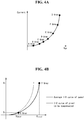
- FIG. 4A illustrates that a reference curve equation is obtained in the external compensation method of FIG. 3 .
- FIG. 4B illustrates an average I-V curve of a display panel and an I-V curve of a pixel to be compensated in the external compensation method of FIG. 3 .
- FIG. 4C illustrates an average I-V curve of a display panel, an I-V curve of a pixel to be compensated, and an I-V curve of a compensated pixel in the external compensation method of FIG. 3 .
- an electroluminescent display may include a display panel 10, a driver IC (or referred to as "D-IC") 20, a compensation IC 30, a host system 40, and a storage memory 50.
- D-IC driver IC
- D-IC compensation IC
- host system 40 host system 40
- storage memory 50 storage memory 50.
- the display panel 10 includes a plurality of pixels PXL and a plurality of signal lines.
- the signal lines may include data lines 140 for supplying data signals (e.g., analog data voltages) to the pixels PXL and gate lines 150 for supplying gate signals to the pixels PXL.
- the gate signal may include a plurality of gate signals including a first gate signal SCAN1 and a second gate signal SCAN2.
- each gate line 150 may include a first gate line 150A for supplying the first gate signal SCAN1 and a second gate line 150B for supplying the second gate signal SCAN2 (see FIG. 8 ).
- the gate signal may include one gate signal depending on a circuit configuration of the pixel PXL.
- each gate line 150 may include one gate line. Embodiments are not limited to exemplary configurations of the gate signal and the gate line 150.
- Electrical characteristics (e.g., a threshold voltage of an organic light emitting diode (OLED)) of the pixel PXL may be sensed through not a separate sensing line but the data line 140.
- OLED organic light emitting diode
- the pixels PXL of the display panel 10 are disposed in a matrix to form a pixel array.
- Each pixel PXL may be connected to one of the data lines 140 and at least one of the gate lines 150.
- Each pixel PXL is configured to receive a high potential driving power VDD and a low potential driving power VSS from a power generator (see FIG. 8 ).
- the power generator may supply the high potential driving power VDD to the pixel PXL through a high potential pixel power line or a pad and may supply the low potential driving power VSS to the pixel PXL through a low potential pixel power line or a pad.
- the gate driver 15 may generate a display gate signal necessary for a display drive operation and a sensing gate signal necessary for a sensing drive operation.
- each of the display gate signal and the sensing gate signal may include a first gate signal SCAN1 and a second gate signal SCAN2.
- the gate driver 15 may generate a first display gate signal SCAN1 to supply the first display gate signal SCAN1 to the first gate line 150A, and may generate a second display gate signal SCAN2 to supply the second display gate signal SCAN2 to the second gate line 150B.
- the first display gate signal SCAN1 and the second display gate signal SCAN2 are signals synchronized with an application timing of a display data voltage Vdata-DIS.
- the gate driver 15 may generate a first sensing gate signal SCAN1 to supply the first sensing gate signal SCAN1 to the first gate line 150A, and may generate a second sensing gate signal SCAN2 to supply the second sensing gate signal SCAN2 to the second gate line 150B.
- the gate driver 15 may be directly formed on a lower substrate of the display panel 10 in a gate driver-in panel (GIP) manner.
- the gate driver 15 may be formed in a non-display area (i.e., a bezel area) outside the pixel array of the display panel 10 through the same TFT process as the pixel array.
- the driver IC 20 is connected to the data line 140 of the display panel 10 through a channel terminal CH.
- the driver IC 20 may include a timing controller 21 and a data driver 25.
- the timing controller 21 may generate a gate timing control signal GDC for controlling operation timing of the gate driver 15 and a data timing control signal DDC for controlling operation timing of the data driver 25 based on timing signals, for example, a vertical sync signal Vsync, a horizontal sync signal Hsync, a dot clock signal DCLK, and a data enable signal DE received from the host system 40.
- the data timing control signal DDC may include a source start pulse, a source sampling clock, and a source output enable signal, and the like, but is not limited thereto.
- the source start pulse controls start timing of data sampling of the data driver 25.
- the source sampling clock is a clock signal that controls sampling timing of data based on a rising edge or a falling edge thereof.
- the source output enable signal controls output timing of the data driver 25.
- the gate timing control signal GDC may include a gate start pulse, a gate shift clock, and the like, but is not limited thereto.
- the gate start pulse is applied to a stage of the gate driver 15 for generating a first output and activates an operation of the stage.
- the gate shift clock is a clock signal that is commonly input to stages and shifts the gate start pulse.
- the timing controller 21 may control a sensing mode for the sensing drive operation and a display mode for the display drive operation in accordance with to a predetermined control sequence.
- the sensing mode digital sensing data S-DATA indicating the electrical characteristics of the pixel PXL is obtained.
- the display mode input image data to be written to the pixels PXL is corrected based on the digital sensing data S-DATA obtained in the sensing mode, the corrected image data is converted into a display data voltage Vdata-DIS, and the display data voltage Vdata-DIS is applied to the pixels PXL.
- the timing controller 21 may differently generate timing control signals for the display drive operation and timing control signals for the sensing drive operation.
- the sensing drive operation may be performed in a vertical blanking interval during the display drive operation, in a power-on sequence interval before the beginning of the display drive operation, or in a power-off sequence interval after the end of the display drive operation under the control of the timing controller 21.
- the sensing drive operation may be performed in a vertical active period during the display drive operation.
- the vertical blanking interval is time, for which input image data is not written, and is arranged between vertical active periods in which input image data corresponding to one frame is written.
- the power-on sequence interval is a transient time between the turn-on of driving power and the beginning of image display.
- the power-off sequence interval is a transient time between the end of image display and the turn-off of driving power.
- the timing controller 21 may control all of operations for the sensing drive operation in accordance with a predetermined sensing process. Namely, the sensing drive operation may be performed in a state (for example, a standby mode, a sleep mode, a low power mode, etc.) where only a screen of the display device is turned off while the system power is being applied.
- a state for example, a standby mode, a sleep mode, a low power mode, etc.
- the data driver 25 includes a sensor 22, a data voltage generator 23, a first switch SW1, and a second switch SW2.
- the data voltage generator 23 may include a digital-to-analog converter (DAC) converting a digital signal into an analog signal and an output buffer (not shown).
- the DAC generates the display data voltage Vdata-DIS or a sensing data voltage Vdata-SEN.
- the data voltage generator 23 converts corrected image data V-DATA into an analog gamma voltage using the DAC and supplies the data lines 140 with a conversion result as the display data voltage Vdata-DIS through the first switch SW1.
- the display data voltage Vdata-DIS supplied to the data lines 140 is applied to the pixels PXL in synchronization with turn-on timing of the display gate signal.
- a gate-to-source voltage of a driving thin film transistor (TFT) included in the pixel PXL is programmed by the display data voltage Vdata-DIS, and a driving current flowing in the driving TFT is determined depending on the gate-to-source voltage of the driving TFT.
- TFT driving thin film transistor
- the data voltage generator 23 In the sensing drive operation, the data voltage generator 23 generates the previously set sensing data voltage Vdata-SEN using the DAC and then supplies the sensing data voltage Vdata-SEN to the data lines 140 through the first switch SW1. In the sensing drive operation, the sensing data voltage Vdata-SEN supplied to the data lines 140 is applied to the pixels PXL in synchronization with turn-on timing of the sensing gate signal.
- the gate-to-source voltage of the driving TFT included in the pixel PXL is programmed by the sensing data voltage Vdata-SEN, and a driving current flowing in the driving TFT is determined depending on the gate-to-source voltage of the driving TFT.
- the sensor 22 may receive and sense the electrical characteristics Vsen of the pixel PXL, for example, the threshold voltage of the OLED included in the pixel PXL through the data line 140 and the second switch SW2. As shown in FIG. 2 , the sensor 22 may include a sensing unit SUT and an analog-to-digital converter (ADC).
- ADC analog-to-digital converter
- the sensing unit SUT may be implemented as a voltage sensing unit including a sample and hold unit. In the sensing drive operation, the sensing unit SUT samples a voltage charged to the data line 14 and supplies a result of sampling to the ADC.
- the ADC converts an analog sampling signal received from the sensing unit SUT into a digital signal and outputs digital sensing data S-DATA indicating the electrical characteristics of the pixel PXL.
- the ADC may be implemented as a flash ADC, an ADC using a tracking method, a successive approximation register ADC, and the like.
- the ADC supplies the digital sensing data S-DATA obtained in the sensing drive operation to the storage memory 50.
- the first switch SW1 and the second switch SW2 may be differently turned on and off in the display drive operation and the sensing drive operation.
- the first switch SW1 is connected between the channel terminal CH and the data voltage generator 23, and the second switch SW2 is connected between the channel terminal CH and the sensor 22.
- the storage memory 50 stores the digital sensing data S-DATA.
- the storage memory 50 may be implemented as a flash memory, but is not limited thereto.
- the compensation IC 30 calculates an offset and a gain for each pixel based on the digital sensing data S-DATA read from the storage memory 50.
- the compensation IC 30 modulates (or corrects) digital image data to be input to the pixels PXL depending on the calculated offset and gain, and supplies the modulated digital image data V-DATA to the driver IC 20.
- the compensation IC 30 may include a compensator 31 and a compensation memory 32.
- the compensation memory 32 allows access to the digital sensing data S-DATA read from the storage memory 50 to the compensator 31.
- the compensation memory 32 may be a random access memory (RAM), for example, a double data rate synchronous dynamic RAM (DDR SDRAM), but is not limited thereto.
- RAM random access memory
- DDR SDRAM double data rate synchronous dynamic RAM
- the compensator 31 may include a compensation algorithm that performs a compensation operation so that a current (I)-voltage (V) curve of a corresponding pixel to be compensated coincides with an average I-V curve.
- the average I-V curve may be obtained through a plurality of sensing operations.
- the compensator 31 performs the sensing of a plurality of gray levels (for example, a total of seven gray levels A to G) and then obtains the following Equation 1 corresponding to the average I-V curve through a known least square method in step S1.
- I a V data ⁇ b c
- Equation 1 "a” is electron mobility of the driving TFT, “b” is a threshold voltage of the driving TFT, and “c” is a physical property value of the driving TFT. “a” and “b” are characteristic values varying over the time, and “c” is a characteristic value independent of time.
- the compensator 31 calculates parameter values a' and b' of the corresponding pixel based on current values I1 and I2 and gray values (gray levels X and Y) (i.e., data voltage values Vdatal and Vdata2 of digital level) measured at two points in step S2.
- I 1 a ′ V data 1 ⁇ b ′ c
- I 2 a ′ V data 2 ⁇ b ′ c
- the compensator 31 may calculate the parameter values a' and b' of the corresponding pixel using a quadratic equation in the above Equation 2.
- the compensator 31 may calculate an offset and a gain for causing the I-V curve of the corresponding pixel to be compensated to coincide with the average I-V curve in step S3.
- the offset and the gain of the compensated pixel are expressed by Equation 3. where "Vcomp" is a compensation voltage.
- the compensator 31 corrects digital image data to be input to the corresponding pixel so that the digital image data corresponds to the compensation voltage Vcomp, in step S4. Icomp indicates the compensation current.
- the host system 40 may supply digital image data to be input to the pixels PXL of the display panel 10 to the compensation IC 30.
- the host system 40 may further supply user input information, for example, digital brightness information to the compensation IC 30.
- the host system 40 may be implemented as an application processor.
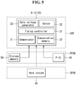
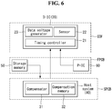
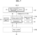
- FIGS. 5 to 7 illustrate various examples of an external compensation module.
- the electroluminescent display may include a driver IC (or referred to as "D-IC") 20 mounted on a chip-on film (COF), a storage memory 50 and a power IC (or referred to as "P-IC") 60 mounted on a flexible printed circuit board (FPCB), and a host system 40 mounted on a system printed circuit board (SPCB), in order to implement an external compensation module.
- D-IC driver IC
- COF chip-on film
- P-IC power IC
- FPCB flexible printed circuit board
- SPCB system printed circuit board
- the driver IC (D-IC) 20 may further include a compensator 31 and a compensation memory 32 in addition to a timing controller 21, a sensor 22, and a data voltage generator 23.
- the external compensation module is implemented by forming the driver IC (D-IC) 20 and a compensation IC 30 (see FIG. 1 ) into one chip.
- the power IC (P-IC) 60 generates various driving powers required to operate the external compensation module.
- the electroluminescent display may include a driver IC (or referred to as "D-IC") 20 mounted on a chip-on film (COF), a storage memory 50 and a power IC (or referred to as "P-IC") 60 mounted on a flexible printed circuit board (FPCB), and a host system 40 mounted on a system printed circuit board (SPCB), in order to implement an external compensation module.
- D-IC driver IC
- COF chip-on film
- P-IC power IC
- FPCB flexible printed circuit board
- SPCB system printed circuit board
- the external compensation module of FIG. 6 is different from the external compensation module of FIG. 5 in that a compensator 31 and a compensation memory 32 are mounted on the host system 40 without being mounted on the driver IC 20.
- the external compensation module of FIG. 6 is implemented by integrating a compensation IC 30 (see FIG. 1 ) into the host system 40 and is meaningful in that the configuration of the driver IC 20 can be simplified.
- the electroluminescent display may include a driver IC (or referred to as "D-IC") 20 mounted on a chip-on film (COF), a storage memory 50, a compensation IC 30, a compensation memory 32, and a power IC (or referred to as "P-IC") 60 mounted on a flexible printed circuit board (FPCB), and a host system 40 mounted on a system printed circuit board (SPCB), in order to implement an external compensation module.
- D-IC driver IC
- COF chip-on film
- P-IC power IC
- FPCB flexible printed circuit board
- SPCB system printed circuit board
- the external compensation module of FIG. 7 is different from the external compensation modules of FIGS. 5 and 6 in that the configuration of the driver IC 20 is further simplified by mounting only a data voltage generator 23 and a sensor 22 in the driver IC 20, and a timing controller 21 and the compensator 31 are mounted in the compensation IC 30 that is separately manufactured.
- the external compensation module of FIG. 7 can easily perform an uploading and downloading operation of a compensation parameter by together mounting the compensation IC 30, the storage memory 50, and the compensation memory 32 on the flexible printed circuit board.
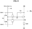
- FIG. 8 is an equivalent circuit diagram of a pixel according to an example embodiment.
- each pixel PXL includes an OLED, a driving TFT DT, a storage capacitor Cst, a first switching TFT ST1, and a second switching TFT ST2.
- the TFTs constituting the pixel PXL may be implemented as p-type metal-oxide semiconductor (PMOS) transistors.
- a first gate signal SCAN1 may be a first sensing gate signal
- a second gate signal SCAN2 may be a second sensing gate signal
- a data voltage Vdata supplied to the data line 140 by the data voltage generator 23 may be a sensing data voltage Vdata-SEN.
- the OLED is a light emitting element that emits light with a driving current input from the driving TFT DT.
- the OLED includes an anode electrode, a cathode electrode, and an organic compound layer between the anode electrode and the cathode electrode.
- the anode electrode is connected to a second node N2 that is a drain electrode of the driving TFT DT.
- the cathode electrode is connected to an input terminal of a low potential driving power VSS.
- a gray level of an image displayed on a corresponding pixel PXL is determined depending on an amount of light emitted by the OLED.
- the driving TFT DT is a driving element controlling a driving current input to the OLED depending on a gate-to-source voltage Vgs of the driving TFT DT.
- the driving TFT DT includes a gate electrode (or referred to as “control electrode”) connected to a first node N1, a source electrode (or referred to as “first electrode”) connected to an input terminal of a high potential driving power VDD, and the drain electrode (or referred to as "second electrode”) connected to the second node N2.
- the gate-to-source voltage Vgs of the driving TFT DT is a difference between a voltage of the high potential driving power VDD and a voltage of the first node N1.
- the storage capacitor Cst is connected between the high potential driving power VDD and the first node N1.
- the storage capacitor Cst holds the gate-to-source voltage Vgs of the driving TFT DT for a particular time.
- the first switching TFT ST1 applies the data voltage Vdata on the data line 140 to the first node N1 in response to the first gate signal SCAN1.
- the first switching TFT ST1 includes a gate electrode (or referred to as “control electrode”) connected to the first gate line 150A, a source electrode (or referred to as “first electrode”) connected to the data line 140, and a drain electrode (or referred to as “second electrode”) connected to the first node N1.
- the second switching TFT ST2 switches on and off a current flow between the second node N2 and the data line 140 in response to the second gate signal SCAN2.
- the second switching TFT ST2 includes a gate electrode (or referred to as “control electrode”) connected to the second gate line 150B, a drain electrode (or referred to as “first electrode”) connected to the data line 140, and a source electrode (or referred to as "second electrode”) connected to the second node N2.
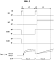
- FIG. 9 is a driving waveform diagram for sensing electrical characteristics of an electroluminescent display according to an example embodiment.
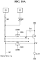
- FIG. 10A is an equivalent circuit diagram of first and second switches and a pixel during a first programming period shown in FIG. 9 .
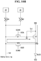
- FIG. 10B is an equivalent circuit diagram of first and second switches and a pixel during a degradation tracking period shown in FIG. 9 .
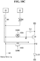
- FIG. 10C is an equivalent circuit diagram of first and second switches and a pixel during a second programming period shown in FIG. 9 .
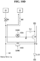
- FIG. 10D is an equivalent circuit diagram of first and second switches and a pixel during a sensing period shown in FIG. 9 .
- a sensing drive operation may be implemented through a first programming period 1, a degradation tracking period 2, a second programming period 3, and a sensing period 4 that are successively arranged.
- first and second data voltages Vdatal and Vdata2 are sensing data voltages.
- the second switch SW2 is turned off (OFF), and the first switch SW1, the first switching TFT ST1, and the second switching TFT ST2 are turned on (ON).
- the first data voltage Vdatal generated in the data voltage generator 23 is applied to the first node N1 through the first switch SW1 and the first switching TFT ST1
- the first data voltage Vdatal is applied to the second node N2 through the first switch SW1 and the second switching TFT ST2.
- the driving TFT DT satisfies turn-on condition in the first programming period 1. Further, the anode electrode of the OLED is initialized to the first data voltage Vdatal.
- the first and second switches SW1 and SW2 are turned off, and the first and second switching TFTs ST1 and ST2 are turned on.
- a voltage of the first node N1 and a voltage of the second node N2 increase up to a threshold voltage of the OLED by a current flowing in the driving TFT DT.
- the voltage of the second node N2 increases in proportion to (in direct proportion to) the degradation of the OLED.
- a voltage of the data line 140 increases in proportion to the degradation of the OLED during the degradation tracking period 2.
- the first switch SW1 and the second switching TFT ST2 are turned on, and the second switch SW2 and the first switching TFT ST1 are turned off.
- the second data voltage Vdata2 generated in the data voltage generator 23 is applied to the second node N2 through the first switch SW1 and the second switching TFT ST2.
- the second data voltage Vdata2 is greater than the first data voltage Vdatal and is less than the threshold voltage of the OLED.
- the second data voltage Vdata2 is less than the threshold voltage of the OLED as described above, it is easy to match voltage levels of analog sensing data with an input range of the ADC.
- the second switch SW2 and the second switching TFT ST2 are turned on, and the first switch SW1 and the first switching TFT ST1 are turned off.
- the current flows in the driving TFT DT by the gate-to-source voltage stored in the storage capacitor Cst, and as a result, the voltage of the second node N2 and the voltage of the data line 140 connected to the second node N2 increase.
- a change in the voltage of the second node N2, which decreases depending on the driving current, through the data line 140 is read out, and a rising slope of the voltage of the data line 140 is less after the degradation of the OLED than before the degradation of the OLED.
- the threshold voltage of the OLED increases. Therefore, relatively more charges are accumulated on the anode electrode of the OLED than before the degradation of the OLED. Hence, a charging rate of the data line is reduced. As a result, the voltage of the data line 140 increases more slowly after the degradation of the OLED than before the degradation of the OLED.
- the sensing drive operation it is possible to sense the degradation of the OLED even in a PMOS pixel structure. Furthermore, because the threshold voltage of the OLED is sensed through the data line instead of the sensing line of the sharing structure, the OLED can be directly sensed.
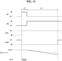
- FIG. 11 is a driving waveform diagram for sensing electrical characteristics of an electroluminescent display according to another example.
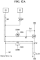
- FIG. 12A is an equivalent circuit diagram of first and second switches and a pixel during an initialization period shown in FIG. 11 .
- FIG. 12B is an equivalent circuit diagram of first and second switches and a pixel during a sensing period shown in FIG. 11 .
- a sensing drive operation may be implemented through an initialization period 1' and a sensing period 2' that are successively arranged.
- a data voltage Vdata is a sensing data voltage.
- a second switch SW2 and a first switching TFT ST1 are turned off (OFF), and a first switch SW1 and a second switching TFT ST2 are turned on (ON).
- the data voltage Vdata generated in a data voltage generator 23 is applied to a second node N2 through the first switch SW1 and the second switching TFT ST2.
- the data voltage Vdata is set to be greater than an threshold voltage of an OLED so that a discharge is performed through the OLED.
- the driving TFT DT satisfies turn-off condition, and an anode electrode of the OLED is initialized to the data voltage Vdata.
- the first switch SW1 and the first switching TFT ST1 are turned off, and the second switch SW2 and the second switching TFT ST2 are turned on, a change in a voltage of the second node N2, which decreases as the data voltage Vdata is discharged through the OLED, through the data line 140 is read out.
- the data voltage Vdata that has been charged to the anode electrode of the OLED is discharged through the OLED during the sensing period 2', and as a result, a voltage of the second node N2 is gradually reduced.
- a rate of a reduction in the voltage of the second node N2 decreases.
- a current flowing through the OLED decreases due to an increase in a resistance component of the OLED as the degradation of the OLED proceeds.
- the second node N2 is connected to a data line 140 during the sensing period 2', a falling slope of a voltage of the data line 140 is less after the degradation of the OLED than before the degradation of the OLED during the sensing period 2'.
- embodiments can sense the threshold voltage of the OLED without reducing the line design margin of the display panel by using the data lines for data supply in the sensing drive operation instead of the separate sensing line according to the related art.
Landscapes
- Engineering & Computer Science (AREA)
- Physics & Mathematics (AREA)
- Computer Hardware Design (AREA)
- General Physics & Mathematics (AREA)
- Theoretical Computer Science (AREA)
- Control Of Indicators Other Than Cathode Ray Tubes (AREA)
- Electroluminescent Light Sources (AREA)
- Control Of El Displays (AREA)
Claims (7)
- Dispositif d'affichage électroluminescent comprenant :un panneau d'affichage (10) comprenant une pluralité de pixels, une pluralité de lignes de grille (150) et une pluralité de lignes de données ; etun circuit intégré d'attaque (20) raccordé à une ligne de données (140) de la pluralité de lignes de données au moyen d'une borne de canal (CH),dans lequel le circuit intégré d'attaque (20) comprend :un générateur de tension de données (23) configuré pour générer une tension de données à fournir à un pixel (PXL) de la pluralité de pixels ;un premier commutateur (SW1) raccordé entre la borne de canal (CH) et le générateur de tension de données (23) ;un capteur (22) configuré pour détecter des caractéristiques électriques du pixel (PXL) ; etun second commutateur (SW2) raccordé entre la borne de canal (CH) et le capteur (22),dans lequel chaque pixel comprend :un transistor à couches minces, TFT, d'attaque (DT) comprenant une électrode de commande raccordée à un premier noeud (N1), une première électrode raccordée à une puissance d'excitation à potentiel élevé (VDD) et une seconde électrode raccordée à un second noeud (N2) ;une diode électroluminescente organique (OLED) raccordée entre le second noeud (N2) et une puissance d'excitation à faible potentiel (VSS) ;un premier transistor TFT de commutation (ST1) comprenant une électrode de commande raccordée à une première ligne de grille (150A) alimentée avec un premier signal de grille, une première électrode raccordée à la ligne de données (140) et une seconde électrode raccordée au premier noeud (N1) ;un second transistor TFT de commutation (ST2) comprenant une électrode de commande raccordée à une seconde ligne de grille (150B) alimentée avec un second signal de grille, une première électrode raccordée à la ligne de données (140) et une seconde électrode raccordée au second noeud (N2) ; etun condensateur de stockage (Cst) raccordé entre la puissance d'excitation à potentiel élevé et le premier noeud (N1) ;dans lequel, pendant une première période de programmation, le premier commutateur, le premier transistor TFT de commutation et le second transistor TFT de commutation sont configurés pour être mis sous tension et le second commutateur est configuré pour être désactivé,dans lequel, pendant une période de suivi de dégradation après la première période de programmation, les premier et second commutateurs sont configurés pour être désactivés et les premier et second transistors TFT de commutation sont configurés pour être mis sous tension,dans lequel, pendant une seconde période de programmation après la période de suivi de dégradation, le premier commutateur, le premier commutateur et le second transistor TFT de commutation sont configurés pour être mis sous tension et le second commutateur et le premier transistor TFT de commutation sont configurés pour être mis hors tension, etdans lequel, pendant une première période de détection après la seconde période de programmation, le second commutateur et le second transistor TFT de commutation sont configurés pour être mis sous tension et le premier commutateur et le premier transistor TFT de commutation sont configurés pour être mis hors tension.
- Dispositif d'affichage électroluminescent selon la revendication 1, dans lequel le générateur de tension de données est configuré pour fournir une première tension de données à la ligne de données pendant la première période de programmation et la période de suivi de dégradation et pour fournir une seconde tension de données supérieure à la première tension de données à la ligne de données pendant la seconde période de programmation.
- Dispositif d'affichage électroluminescent selon la revendication 2, dans lequel une différence entre une tension de la puissance d'excitation à potentiel élevé et la première tension de données est supérieure à une tension de seuil du transistor TFT d'attaque.
- Dispositif d'affichage électroluminescent selon l'une quelconque des revendications 1 à 3, dans lequel une tension de la ligne de données est configurée pour augmenter de manière proportionnelle à une dégradation de la diode OLED pendant la période de suivi de dégradation, et
dans lequel, pendant la première période de détection, une pente ascendante de la tension de la ligne de données est configurée pour être plus faible après la dégradation de la diode OLED qu'avant la dégradation de la diode OLED. - Dispositif d'affichage électroluminescent selon l'une quelconque des revendications précédentes, dans lequel le transistor TFT d'attaque, le premier transistor TFT de commutation et le second transistor TFT de commutation sont mis en oeuvre sous la forme de transistors à semi-conducteur à oxyde métallique de type P (PMOS).
- Procédé de détection de caractéristiques électriques d'un dispositif d'affichage électroluminescent selon la revendication 1, le procédé consistant :pendant la première période de programmation, à appliquer une première tension de données au premier noeud et au second noeud par le biais de la ligne de données pour mettre sous tension le transistor TFT d'attaque ;pendant la période de suivi de dégradation après la première période de programmation, à appliquer un courant d'attaque à la diode OLED à partir du transistor TFT d'attaque pour définir une tension du second noeud en fonction d'une dégradation de la diode OLED ;pendant la seconde période de programmation après la période de suivi de dégradation, à appliquer une seconde tension de données supérieure à la première tension de données au second noeud par le biais de la ligne de données ; etpendant la première période de détection après la seconde période de programmation, à lire un changement de la tension du second noeud, qui diminue en fonction du courant d'attaque, par le biais de la ligne de données.
- Procédé selon la revendication 6,
dans lequel une tension de la ligne de données raccordée au second noeud augmente de manière proportionnelle à la dégradation de la diode OLED pendant la période de suivi de dégradation, et
dans lequel, pendant la première période de détection, une pente ascendante de la tension de la ligne de données raccordée au second noeud est plus faible après la dégradation de la diode OLED qu'avant la dégradation de la diode OLED.
Applications Claiming Priority (1)
| Application Number | Priority Date | Filing Date | Title |
|---|---|---|---|
| KR1020160159578A KR102633409B1 (ko) | 2016-11-28 | 2016-11-28 | 전계발광 표시장치와 그의 전기적 특성 센싱방법 |
Publications (3)
| Publication Number | Publication Date |
|---|---|
| EP3327714A2 EP3327714A2 (fr) | 2018-05-30 |
| EP3327714A3 EP3327714A3 (fr) | 2018-06-13 |
| EP3327714B1 true EP3327714B1 (fr) | 2019-08-21 |
Family
ID=60484218
Family Applications (1)
| Application Number | Title | Priority Date | Filing Date |
|---|---|---|---|
| EP17204173.3A Active EP3327714B1 (fr) | 2016-11-28 | 2017-11-28 | Affichage électroluminescent et procédé de détection des caractéristiques électriques d'affichage électroluminescent |
Country Status (4)
| Country | Link |
|---|---|
| US (1) | US10460662B2 (fr) |
| EP (1) | EP3327714B1 (fr) |
| KR (1) | KR102633409B1 (fr) |
| CN (1) | CN108122531B (fr) |
Families Citing this family (21)
| Publication number | Priority date | Publication date | Assignee | Title |
|---|---|---|---|---|
| US10424247B2 (en) * | 2017-04-28 | 2019-09-24 | Shenzhen China Star Optoelectronics Semiconductor Display Technology Co., Ltd | AMOLED driving circuit and AMOLED display device |
| US10984713B1 (en) * | 2018-05-10 | 2021-04-20 | Apple Inc. | External compensation for LTPO pixel for OLED display |
| KR102560746B1 (ko) * | 2018-11-16 | 2023-07-27 | 엘지디스플레이 주식회사 | 유기발광 표시장치와 그 구동방법 |
| US10964238B2 (en) * | 2018-12-28 | 2021-03-30 | Facebook Technologies, Llc | Display device testing and control |
| CN110062944B (zh) * | 2019-03-13 | 2022-03-29 | 京东方科技集团股份有限公司 | 像素电路及其驱动方法、显示装置 |
| KR102795750B1 (ko) * | 2019-04-22 | 2025-04-15 | 삼성전자주식회사 | 디스플레이 구동 회로 및 이의 동작 방법 |
| CN110223647A (zh) * | 2019-05-06 | 2019-09-10 | 惠科股份有限公司 | 驱动电路以及显示装置 |
| KR102712154B1 (ko) | 2019-05-22 | 2024-09-30 | 삼성전자주식회사 | 디스플레이 구동 회로 및 이를 포함하는 디스플레이 장치 |
| KR102686300B1 (ko) * | 2019-07-23 | 2024-07-22 | 삼성디스플레이 주식회사 | 표시장치의 열화 보상 방법 |
| EP4016510B1 (fr) | 2019-08-14 | 2024-04-10 | BOE Technology Group Co., Ltd. | Circuit de pixels et procédé d'attaque associé, substrat matriciel et dispositif d'affichage |
| US12142207B2 (en) | 2020-03-31 | 2024-11-12 | Apple, Inc. | Configurable pixel uniformity compensation for OLED display non-uniformity compensation based on scaling factors |
| US11257407B2 (en) | 2020-04-23 | 2022-02-22 | Facebook Technologies, Llc | Display diagnostic system |
| KR102771827B1 (ko) * | 2020-10-16 | 2025-02-25 | 엘지디스플레이 주식회사 | 표시장치, 구동회로 및 구동방법 |
| KR102662235B1 (ko) * | 2020-11-12 | 2024-05-02 | 엘지디스플레이 주식회사 | 전계발광 표시장치 |
| KR102854037B1 (ko) * | 2020-12-17 | 2025-09-02 | 엘지디스플레이 주식회사 | 발광표시장치 및 이의 구동방법 |
| TWI795852B (zh) * | 2021-07-23 | 2023-03-11 | 連恩微電子有限公司 | 切換控制電路以及光學感控電路 |
| KR102881833B1 (ko) * | 2021-10-08 | 2025-11-07 | 주식회사 엘엑스세미콘 | 디스플레이 패널의 화소를 구동하는 집적회로, 화소 구동 장치, 및 화소 오류 검출 방법 |
| KR102892509B1 (ko) * | 2022-05-30 | 2025-12-01 | 삼성디스플레이 주식회사 | 표시 시스템 및 이의 구동 방법 |
| CN116434702B (zh) * | 2023-04-27 | 2024-09-20 | 惠科股份有限公司 | 像素结构、显示面板、控制方法和显示装置 |
| US12307933B1 (en) | 2024-04-26 | 2025-05-20 | Dell Products L.P. | Organic light emitting diode display film pixel shifting with temporal segmented image tracking |
| US12456420B1 (en) | 2024-04-26 | 2025-10-28 | Dell Products L.P. | Organic light emitting diode display film comfort state personalization by machine learning |
Family Cites Families (26)
| Publication number | Priority date | Publication date | Assignee | Title |
|---|---|---|---|---|
| SG120075A1 (en) * | 2001-09-21 | 2006-03-28 | Semiconductor Energy Lab | Semiconductor device |
| JP2004318093A (ja) * | 2003-03-31 | 2004-11-11 | Sanyo Electric Co Ltd | 発光ディスプレイ及びその駆動方法及びエレクトロルミネッセンス表示回路及びエレクトロルミネッセンスディスプレイ |
| KR100599724B1 (ko) * | 2003-11-20 | 2006-07-12 | 삼성에스디아이 주식회사 | 표시 패널, 이를 이용한 발광 표시 장치 및 그 구동 방법 |
| US10187133B2 (en) | 2004-04-02 | 2019-01-22 | Rearden, Llc | System and method for power control and antenna grouping in a distributed-input-distributed-output (DIDO) network |
| US9799246B2 (en) * | 2011-05-20 | 2017-10-24 | Ignis Innovation Inc. | System and methods for extraction of threshold and mobility parameters in AMOLED displays |
| KR100604066B1 (ko) * | 2004-12-24 | 2006-07-24 | 삼성에스디아이 주식회사 | 화소 및 이를 이용한 발광 표시장치 |
| KR100637203B1 (ko) * | 2005-01-07 | 2006-10-23 | 삼성에스디아이 주식회사 | 유기 전계발광 표시장치 및 그 동작방법 |
| KR100707623B1 (ko) * | 2005-03-19 | 2007-04-13 | 한양대학교 산학협력단 | 화소 및 이를 이용한 발광 표시장치 |
| KR101186254B1 (ko) * | 2006-05-26 | 2012-09-27 | 엘지디스플레이 주식회사 | 유기 발광다이오드 표시장치와 그의 구동방법 |
| KR100858615B1 (ko) * | 2007-03-22 | 2008-09-17 | 삼성에스디아이 주식회사 | 유기전계발광 표시장치 및 그의 구동방법 |
| KR100893482B1 (ko) * | 2007-08-23 | 2009-04-17 | 삼성모바일디스플레이주식회사 | 유기전계발광 표시장치 및 그의 구동방법 |
| KR101416904B1 (ko) * | 2007-11-07 | 2014-07-09 | 엘지디스플레이 주식회사 | 유기전계발광 표시장치의 화소 구동 장치 |
| US8405582B2 (en) * | 2008-06-11 | 2013-03-26 | Samsung Display Co., Ltd. | Organic light emitting display and driving method thereof |
| KR101150163B1 (ko) * | 2009-10-30 | 2012-05-25 | 주식회사 실리콘웍스 | 유기발광다이오드 표시장치의 구동 회로 및 방법 |
| KR101201722B1 (ko) * | 2010-02-23 | 2012-11-15 | 삼성디스플레이 주식회사 | 유기 발광 표시 장치 및 그의 구동 방법 |
| KR101073226B1 (ko) * | 2010-03-17 | 2011-10-12 | 삼성모바일디스플레이주식회사 | 유기전계발광 표시장치 |
| US9236011B2 (en) * | 2011-08-30 | 2016-01-12 | Lg Display Co., Ltd. | Organic light emitting diode display device for pixel current sensing in the sensing mode and pixel current sensing method thereof |
| KR101536129B1 (ko) * | 2011-10-04 | 2015-07-14 | 엘지디스플레이 주식회사 | 유기발광 표시장치 |
| KR101350592B1 (ko) * | 2011-12-12 | 2014-01-16 | 엘지디스플레이 주식회사 | 유기발광 표시장치 |
| KR101985435B1 (ko) * | 2012-11-30 | 2019-06-05 | 삼성디스플레이 주식회사 | 화소부 및 이를 포함하는 유기 전계 발광 표시 장치 |
| KR101688923B1 (ko) * | 2013-11-14 | 2016-12-23 | 엘지디스플레이 주식회사 | 유기발광표시장치 및 그 구동방법 |
| CN104751771B (zh) * | 2013-12-25 | 2017-09-29 | 昆山国显光电有限公司 | 像素电路结构、有源矩阵有机发光显示器件及其驱动方法 |
| KR102085167B1 (ko) * | 2013-12-31 | 2020-03-06 | 엘지디스플레이 주식회사 | 유기발광다이오드 표시장치 및 그의 구동방법 |
| WO2015190407A1 (fr) * | 2014-06-10 | 2015-12-17 | シャープ株式会社 | Dispositif d'affichage et son procédé de commande |
| KR102404485B1 (ko) * | 2015-01-08 | 2022-06-02 | 삼성디스플레이 주식회사 | 유기 발광 표시 장치 |
| KR20160089932A (ko) * | 2015-01-20 | 2016-07-29 | 삼성디스플레이 주식회사 | 표시장치 및 표시장치의 구동방법 |
-
2016
- 2016-11-28 KR KR1020160159578A patent/KR102633409B1/ko active Active
-
2017
- 2017-11-03 US US15/802,877 patent/US10460662B2/en active Active
- 2017-11-09 CN CN201711096636.0A patent/CN108122531B/zh active Active
- 2017-11-28 EP EP17204173.3A patent/EP3327714B1/fr active Active
Non-Patent Citations (1)
| Title |
|---|
| None * |
Also Published As
| Publication number | Publication date |
|---|---|
| EP3327714A3 (fr) | 2018-06-13 |
| US10460662B2 (en) | 2019-10-29 |
| CN108122531B (zh) | 2020-08-25 |
| US20180151112A1 (en) | 2018-05-31 |
| CN108122531A (zh) | 2018-06-05 |
| KR20180061476A (ko) | 2018-06-08 |
| KR102633409B1 (ko) | 2024-02-07 |
| EP3327714A2 (fr) | 2018-05-30 |
Similar Documents
| Publication | Publication Date | Title |
|---|---|---|
| EP3327714B1 (fr) | Affichage électroluminescent et procédé de détection des caractéristiques électriques d'affichage électroluminescent | |
| US10580356B2 (en) | Driver integrated circuit for external compensation and display device including the same | |
| CN104658474B (zh) | 有机发光显示器和补偿有机发光显示器的阈值电压的方法 | |
| US11011116B2 (en) | External compensation for a display device using varying gate pulse timing | |
| US11217171B2 (en) | Organic light emitting display and method of sensing deterioration of the same | |
| EP3113163B1 (fr) | Dispositif et procédé de détection de tension de seuil drovomg tft inclus dans un affichage électroluminescent organique | |
| US10593268B2 (en) | External compensation for a display device and method of driving the same | |
| US10930210B2 (en) | Organic light-emitting diode display capable of reducing kickback effect | |
| US9514681B2 (en) | Pixel circuit for increasing accuracy of current sensing | |
| US10770007B2 (en) | Driving circuit for real-time external compensation and electroluminescent display including the same | |
| EP2881932B1 (fr) | Affichage électroluminescent organique et procédé de compensation de qualité d'image de celui-ci | |
| US9336713B2 (en) | Organic light emitting display and driving method thereof | |
| US9495909B2 (en) | Organic light emitting display | |
| US10565927B2 (en) | Electroluminescent display and method of compensating for electrical characteristics of electroluminescent display | |
| US10424254B2 (en) | Driver integrated circuit and display device including the same | |
| KR20180068175A (ko) | 외부 보상용 드라이버 집적회로와 그를 포함한 표시장치, 및 표시장치의 데이터 보정방법 | |
| KR20180057285A (ko) | 외부 보상용 드라이버 집적회로와 그를 포함한 표시장치, 및 표시장치의 데이터 보정방법 | |
| KR20180059189A (ko) | 외부 보상용 드라이버 집적회로와 그를 포함한 표시장치 | |
| KR102542871B1 (ko) | 센싱장치 및 이를 포함한 유기발광 표시장치 |
Legal Events
| Date | Code | Title | Description |
|---|---|---|---|
| PUAI | Public reference made under article 153(3) epc to a published international application that has entered the european phase |
Free format text: ORIGINAL CODE: 0009012 |
|
| STAA | Information on the status of an ep patent application or granted ep patent |
Free format text: STATUS: REQUEST FOR EXAMINATION WAS MADE |
|
| PUAL | Search report despatched |
Free format text: ORIGINAL CODE: 0009013 |
|
| 17P | Request for examination filed |
Effective date: 20171128 |
|
| AK | Designated contracting states |
Kind code of ref document: A2 Designated state(s): AL AT BE BG CH CY CZ DE DK EE ES FI FR GB GR HR HU IE IS IT LI LT LU LV MC MK MT NL NO PL PT RO RS SE SI SK SM TR |
|
| AX | Request for extension of the european patent |
Extension state: BA ME |
|
| AK | Designated contracting states |
Kind code of ref document: A3 Designated state(s): AL AT BE BG CH CY CZ DE DK EE ES FI FR GB GR HR HU IE IS IT LI LT LU LV MC MK MT NL NO PL PT RO RS SE SI SK SM TR |
|
| AX | Request for extension of the european patent |
Extension state: BA ME |
|
| RIC1 | Information provided on ipc code assigned before grant |
Ipc: G09G 3/20 20060101ALI20180508BHEP Ipc: G09G 3/3233 20160101AFI20180508BHEP Ipc: G09G 3/3291 20160101ALI20180508BHEP |
|
| STAA | Information on the status of an ep patent application or granted ep patent |
Free format text: STATUS: EXAMINATION IS IN PROGRESS |
|
| RBV | Designated contracting states (corrected) |
Designated state(s): AL AT BE BG CH CY CZ DE DK EE ES FI FR GB GR HR HU IE IS IT LI LT LU LV MC MK MT NL NO PL PT RO RS SE SI SK SM TR |
|
| 17Q | First examination report despatched |
Effective date: 20181217 |
|
| REG | Reference to a national code |
Ref country code: DE Ref legal event code: R079 Ref document number: 602017006344 Country of ref document: DE Free format text: PREVIOUS MAIN CLASS: G09G0003323300 Ipc: G09G0003000000 |
|
| GRAP | Despatch of communication of intention to grant a patent |
Free format text: ORIGINAL CODE: EPIDOSNIGR1 |
|
| STAA | Information on the status of an ep patent application or granted ep patent |
Free format text: STATUS: GRANT OF PATENT IS INTENDED |
|
| RIC1 | Information provided on ipc code assigned before grant |
Ipc: G09G 3/20 20060101ALI20190214BHEP Ipc: G09G 3/3233 20160101ALI20190214BHEP Ipc: G09G 3/3291 20160101ALI20190214BHEP Ipc: G09G 3/00 20060101AFI20190214BHEP |
|
| INTG | Intention to grant announced |
Effective date: 20190306 |
|
| GRAS | Grant fee paid |
Free format text: ORIGINAL CODE: EPIDOSNIGR3 |
|
| GRAA | (expected) grant |
Free format text: ORIGINAL CODE: 0009210 |
|
| STAA | Information on the status of an ep patent application or granted ep patent |
Free format text: STATUS: THE PATENT HAS BEEN GRANTED |
|
| AK | Designated contracting states |
Kind code of ref document: B1 Designated state(s): AL AT BE BG CH CY CZ DE DK EE ES FI FR GB GR HR HU IE IS IT LI LT LU LV MC MK MT NL NO PL PT RO RS SE SI SK SM TR |
|
| REG | Reference to a national code |
Ref country code: GB Ref legal event code: FG4D |
|
| REG | Reference to a national code |
Ref country code: CH Ref legal event code: EP |
|
| REG | Reference to a national code |
Ref country code: DE Ref legal event code: R096 Ref document number: 602017006344 Country of ref document: DE |
|
| REG | Reference to a national code |
Ref country code: AT Ref legal event code: REF Ref document number: 1170644 Country of ref document: AT Kind code of ref document: T Effective date: 20190915 |
|
| REG | Reference to a national code |
Ref country code: IE Ref legal event code: FG4D |
|
| REG | Reference to a national code |
Ref country code: NL Ref legal event code: FP |
|
| REG | Reference to a national code |
Ref country code: LT Ref legal event code: MG4D |
|
| PG25 | Lapsed in a contracting state [announced via postgrant information from national office to epo] |
Ref country code: FI Free format text: LAPSE BECAUSE OF FAILURE TO SUBMIT A TRANSLATION OF THE DESCRIPTION OR TO PAY THE FEE WITHIN THE PRESCRIBED TIME-LIMIT Effective date: 20190821 Ref country code: NO Free format text: LAPSE BECAUSE OF FAILURE TO SUBMIT A TRANSLATION OF THE DESCRIPTION OR TO PAY THE FEE WITHIN THE PRESCRIBED TIME-LIMIT Effective date: 20191121 Ref country code: SE Free format text: LAPSE BECAUSE OF FAILURE TO SUBMIT A TRANSLATION OF THE DESCRIPTION OR TO PAY THE FEE WITHIN THE PRESCRIBED TIME-LIMIT Effective date: 20190821 Ref country code: BG Free format text: LAPSE BECAUSE OF FAILURE TO SUBMIT A TRANSLATION OF THE DESCRIPTION OR TO PAY THE FEE WITHIN THE PRESCRIBED TIME-LIMIT Effective date: 20191121 Ref country code: HR Free format text: LAPSE BECAUSE OF FAILURE TO SUBMIT A TRANSLATION OF THE DESCRIPTION OR TO PAY THE FEE WITHIN THE PRESCRIBED TIME-LIMIT Effective date: 20190821 Ref country code: LT Free format text: LAPSE BECAUSE OF FAILURE TO SUBMIT A TRANSLATION OF THE DESCRIPTION OR TO PAY THE FEE WITHIN THE PRESCRIBED TIME-LIMIT Effective date: 20190821 Ref country code: PT Free format text: LAPSE BECAUSE OF FAILURE TO SUBMIT A TRANSLATION OF THE DESCRIPTION OR TO PAY THE FEE WITHIN THE PRESCRIBED TIME-LIMIT Effective date: 20191223 |
|
| PG25 | Lapsed in a contracting state [announced via postgrant information from national office to epo] |
Ref country code: IS Free format text: LAPSE BECAUSE OF FAILURE TO SUBMIT A TRANSLATION OF THE DESCRIPTION OR TO PAY THE FEE WITHIN THE PRESCRIBED TIME-LIMIT Effective date: 20191221 Ref country code: LV Free format text: LAPSE BECAUSE OF FAILURE TO SUBMIT A TRANSLATION OF THE DESCRIPTION OR TO PAY THE FEE WITHIN THE PRESCRIBED TIME-LIMIT Effective date: 20190821 Ref country code: RS Free format text: LAPSE BECAUSE OF FAILURE TO SUBMIT A TRANSLATION OF THE DESCRIPTION OR TO PAY THE FEE WITHIN THE PRESCRIBED TIME-LIMIT Effective date: 20190821 Ref country code: GR Free format text: LAPSE BECAUSE OF FAILURE TO SUBMIT A TRANSLATION OF THE DESCRIPTION OR TO PAY THE FEE WITHIN THE PRESCRIBED TIME-LIMIT Effective date: 20191122 Ref country code: AL Free format text: LAPSE BECAUSE OF FAILURE TO SUBMIT A TRANSLATION OF THE DESCRIPTION OR TO PAY THE FEE WITHIN THE PRESCRIBED TIME-LIMIT Effective date: 20190821 Ref country code: ES Free format text: LAPSE BECAUSE OF FAILURE TO SUBMIT A TRANSLATION OF THE DESCRIPTION OR TO PAY THE FEE WITHIN THE PRESCRIBED TIME-LIMIT Effective date: 20190821 |
|
| REG | Reference to a national code |
Ref country code: AT Ref legal event code: MK05 Ref document number: 1170644 Country of ref document: AT Kind code of ref document: T Effective date: 20190821 |
|
| PG25 | Lapsed in a contracting state [announced via postgrant information from national office to epo] |
Ref country code: TR Free format text: LAPSE BECAUSE OF FAILURE TO SUBMIT A TRANSLATION OF THE DESCRIPTION OR TO PAY THE FEE WITHIN THE PRESCRIBED TIME-LIMIT Effective date: 20190821 |
|
| PG25 | Lapsed in a contracting state [announced via postgrant information from national office to epo] |
Ref country code: PL Free format text: LAPSE BECAUSE OF FAILURE TO SUBMIT A TRANSLATION OF THE DESCRIPTION OR TO PAY THE FEE WITHIN THE PRESCRIBED TIME-LIMIT Effective date: 20190821 Ref country code: EE Free format text: LAPSE BECAUSE OF FAILURE TO SUBMIT A TRANSLATION OF THE DESCRIPTION OR TO PAY THE FEE WITHIN THE PRESCRIBED TIME-LIMIT Effective date: 20190821 Ref country code: DK Free format text: LAPSE BECAUSE OF FAILURE TO SUBMIT A TRANSLATION OF THE DESCRIPTION OR TO PAY THE FEE WITHIN THE PRESCRIBED TIME-LIMIT Effective date: 20190821 Ref country code: IT Free format text: LAPSE BECAUSE OF FAILURE TO SUBMIT A TRANSLATION OF THE DESCRIPTION OR TO PAY THE FEE WITHIN THE PRESCRIBED TIME-LIMIT Effective date: 20190821 Ref country code: AT Free format text: LAPSE BECAUSE OF FAILURE TO SUBMIT A TRANSLATION OF THE DESCRIPTION OR TO PAY THE FEE WITHIN THE PRESCRIBED TIME-LIMIT Effective date: 20190821 Ref country code: RO Free format text: LAPSE BECAUSE OF FAILURE TO SUBMIT A TRANSLATION OF THE DESCRIPTION OR TO PAY THE FEE WITHIN THE PRESCRIBED TIME-LIMIT Effective date: 20190821 |
|
| PG25 | Lapsed in a contracting state [announced via postgrant information from national office to epo] |
Ref country code: SK Free format text: LAPSE BECAUSE OF FAILURE TO SUBMIT A TRANSLATION OF THE DESCRIPTION OR TO PAY THE FEE WITHIN THE PRESCRIBED TIME-LIMIT Effective date: 20190821 Ref country code: SM Free format text: LAPSE BECAUSE OF FAILURE TO SUBMIT A TRANSLATION OF THE DESCRIPTION OR TO PAY THE FEE WITHIN THE PRESCRIBED TIME-LIMIT Effective date: 20190821 Ref country code: CZ Free format text: LAPSE BECAUSE OF FAILURE TO SUBMIT A TRANSLATION OF THE DESCRIPTION OR TO PAY THE FEE WITHIN THE PRESCRIBED TIME-LIMIT Effective date: 20190821 Ref country code: IS Free format text: LAPSE BECAUSE OF FAILURE TO SUBMIT A TRANSLATION OF THE DESCRIPTION OR TO PAY THE FEE WITHIN THE PRESCRIBED TIME-LIMIT Effective date: 20200224 |
|
| REG | Reference to a national code |
Ref country code: DE Ref legal event code: R097 Ref document number: 602017006344 Country of ref document: DE |
|
| PLBE | No opposition filed within time limit |
Free format text: ORIGINAL CODE: 0009261 |
|
| STAA | Information on the status of an ep patent application or granted ep patent |
Free format text: STATUS: NO OPPOSITION FILED WITHIN TIME LIMIT |
|
| PG2D | Information on lapse in contracting state deleted |
Ref country code: IS |
|
| PG25 | Lapsed in a contracting state [announced via postgrant information from national office to epo] |
Ref country code: MC Free format text: LAPSE BECAUSE OF FAILURE TO SUBMIT A TRANSLATION OF THE DESCRIPTION OR TO PAY THE FEE WITHIN THE PRESCRIBED TIME-LIMIT Effective date: 20190821 Ref country code: LU Free format text: LAPSE BECAUSE OF NON-PAYMENT OF DUE FEES Effective date: 20191128 |
|
| 26N | No opposition filed |
Effective date: 20200603 |
|
| REG | Reference to a national code |
Ref country code: BE Ref legal event code: MM Effective date: 20191130 |
|
| PG25 | Lapsed in a contracting state [announced via postgrant information from national office to epo] |
Ref country code: SI Free format text: LAPSE BECAUSE OF FAILURE TO SUBMIT A TRANSLATION OF THE DESCRIPTION OR TO PAY THE FEE WITHIN THE PRESCRIBED TIME-LIMIT Effective date: 20190821 |
|
| PG25 | Lapsed in a contracting state [announced via postgrant information from national office to epo] |
Ref country code: IE Free format text: LAPSE BECAUSE OF NON-PAYMENT OF DUE FEES Effective date: 20191128 |
|
| PG25 | Lapsed in a contracting state [announced via postgrant information from national office to epo] |
Ref country code: BE Free format text: LAPSE BECAUSE OF NON-PAYMENT OF DUE FEES Effective date: 20191130 |
|
| PG25 | Lapsed in a contracting state [announced via postgrant information from national office to epo] |
Ref country code: CY Free format text: LAPSE BECAUSE OF FAILURE TO SUBMIT A TRANSLATION OF THE DESCRIPTION OR TO PAY THE FEE WITHIN THE PRESCRIBED TIME-LIMIT Effective date: 20190821 |
|
| REG | Reference to a national code |
Ref country code: CH Ref legal event code: PL |
|
| PG25 | Lapsed in a contracting state [announced via postgrant information from national office to epo] |
Ref country code: HU Free format text: LAPSE BECAUSE OF FAILURE TO SUBMIT A TRANSLATION OF THE DESCRIPTION OR TO PAY THE FEE WITHIN THE PRESCRIBED TIME-LIMIT; INVALID AB INITIO Effective date: 20171128 Ref country code: MT Free format text: LAPSE BECAUSE OF FAILURE TO SUBMIT A TRANSLATION OF THE DESCRIPTION OR TO PAY THE FEE WITHIN THE PRESCRIBED TIME-LIMIT Effective date: 20190821 |
|
| PG25 | Lapsed in a contracting state [announced via postgrant information from national office to epo] |
Ref country code: LI Free format text: LAPSE BECAUSE OF NON-PAYMENT OF DUE FEES Effective date: 20201130 Ref country code: CH Free format text: LAPSE BECAUSE OF NON-PAYMENT OF DUE FEES Effective date: 20201130 |
|
| PG25 | Lapsed in a contracting state [announced via postgrant information from national office to epo] |
Ref country code: MK Free format text: LAPSE BECAUSE OF FAILURE TO SUBMIT A TRANSLATION OF THE DESCRIPTION OR TO PAY THE FEE WITHIN THE PRESCRIBED TIME-LIMIT Effective date: 20190821 |
|
| PGFP | Annual fee paid to national office [announced via postgrant information from national office to epo] |
Ref country code: NL Payment date: 20250922 Year of fee payment: 9 |
|
| PGFP | Annual fee paid to national office [announced via postgrant information from national office to epo] |
Ref country code: GB Payment date: 20250922 Year of fee payment: 9 |
|
| PGFP | Annual fee paid to national office [announced via postgrant information from national office to epo] |
Ref country code: FR Payment date: 20250925 Year of fee payment: 9 |
|
| PGFP | Annual fee paid to national office [announced via postgrant information from national office to epo] |
Ref country code: DE Payment date: 20250922 Year of fee payment: 9 |