EP3330762A1 - Procédé de réglage d'un dispositif optique - Google Patents
Procédé de réglage d'un dispositif optique Download PDFInfo
- Publication number
- EP3330762A1 EP3330762A1 EP17180813.2A EP17180813A EP3330762A1 EP 3330762 A1 EP3330762 A1 EP 3330762A1 EP 17180813 A EP17180813 A EP 17180813A EP 3330762 A1 EP3330762 A1 EP 3330762A1
- Authority
- EP
- European Patent Office
- Prior art keywords
- component
- optical
- spatial direction
- movable component
- optical device
- Prior art date
- Legal status (The legal status is an assumption and is not a legal conclusion. Google has not performed a legal analysis and makes no representation as to the accuracy of the status listed.)
- Granted
Links
Images




Classifications
-
- G—PHYSICS
- G03—PHOTOGRAPHY; CINEMATOGRAPHY; ANALOGOUS TECHNIQUES USING WAVES OTHER THAN OPTICAL WAVES; ELECTROGRAPHY; HOLOGRAPHY
- G03F—PHOTOMECHANICAL PRODUCTION OF TEXTURED OR PATTERNED SURFACES, e.g. FOR PRINTING, FOR PROCESSING OF SEMICONDUCTOR DEVICES; MATERIALS THEREFOR; ORIGINALS THEREFOR; APPARATUS SPECIALLY ADAPTED THEREFOR
- G03F7/00—Photomechanical, e.g. photolithographic, production of textured or patterned surfaces, e.g. printing surfaces; Materials therefor, e.g. comprising photoresists; Apparatus specially adapted therefor
- G03F7/70—Microphotolithographic exposure; Apparatus therefor
- G03F7/70216—Mask projection systems
- G03F7/70308—Optical correction elements, filters or phase plates for manipulating imaging light, e.g. intensity, wavelength, polarisation, phase or image shift
-
- G—PHYSICS
- G03—PHOTOGRAPHY; CINEMATOGRAPHY; ANALOGOUS TECHNIQUES USING WAVES OTHER THAN OPTICAL WAVES; ELECTROGRAPHY; HOLOGRAPHY
- G03F—PHOTOMECHANICAL PRODUCTION OF TEXTURED OR PATTERNED SURFACES, e.g. FOR PRINTING, FOR PROCESSING OF SEMICONDUCTOR DEVICES; MATERIALS THEREFOR; ORIGINALS THEREFOR; APPARATUS SPECIALLY ADAPTED THEREFOR
- G03F7/00—Photomechanical, e.g. photolithographic, production of textured or patterned surfaces, e.g. printing surfaces; Materials therefor, e.g. comprising photoresists; Apparatus specially adapted therefor
- G03F7/70—Microphotolithographic exposure; Apparatus therefor
- G03F7/70058—Mask illumination systems
- G03F7/70141—Illumination system adjustment, e.g. adjustments during exposure or alignment during assembly of illumination system
-
- G—PHYSICS
- G02—OPTICS
- G02B—OPTICAL ELEMENTS, SYSTEMS OR APPARATUS
- G02B17/00—Systems with reflecting surfaces, with or without refracting elements
- G02B17/02—Catoptric systems, e.g. image erecting and reversing system
- G02B17/06—Catoptric systems, e.g. image erecting and reversing system using mirrors only, i.e. having only one curved mirror
-
- G—PHYSICS
- G02—OPTICS
- G02B—OPTICAL ELEMENTS, SYSTEMS OR APPARATUS
- G02B26/00—Optical devices or arrangements for the control of light using movable or deformable optical elements
- G02B26/08—Optical devices or arrangements for the control of light using movable or deformable optical elements for controlling the direction of light
- G02B26/0816—Optical devices or arrangements for the control of light using movable or deformable optical elements for controlling the direction of light by means of one or more reflecting elements
-
- G—PHYSICS
- G02—OPTICS
- G02B—OPTICAL ELEMENTS, SYSTEMS OR APPARATUS
- G02B7/00—Mountings, adjusting means, or light-tight connections, for optical elements
- G02B7/18—Mountings, adjusting means, or light-tight connections, for optical elements for prisms; for mirrors
- G02B7/182—Mountings, adjusting means, or light-tight connections, for optical elements for prisms; for mirrors for mirrors
- G02B7/1822—Mountings, adjusting means, or light-tight connections, for optical elements for prisms; for mirrors for mirrors comprising means for aligning the optical axis
- G02B7/1827—Motorised alignment
- G02B7/1828—Motorised alignment using magnetic means
-
- G—PHYSICS
- G03—PHOTOGRAPHY; CINEMATOGRAPHY; ANALOGOUS TECHNIQUES USING WAVES OTHER THAN OPTICAL WAVES; ELECTROGRAPHY; HOLOGRAPHY
- G03F—PHOTOMECHANICAL PRODUCTION OF TEXTURED OR PATTERNED SURFACES, e.g. FOR PRINTING, FOR PROCESSING OF SEMICONDUCTOR DEVICES; MATERIALS THEREFOR; ORIGINALS THEREFOR; APPARATUS SPECIALLY ADAPTED THEREFOR
- G03F7/00—Photomechanical, e.g. photolithographic, production of textured or patterned surfaces, e.g. printing surfaces; Materials therefor, e.g. comprising photoresists; Apparatus specially adapted therefor
- G03F7/70—Microphotolithographic exposure; Apparatus therefor
- G03F7/70008—Production of exposure light, i.e. light sources
- G03F7/70033—Production of exposure light, i.e. light sources by plasma extreme ultraviolet [EUV] sources
-
- G—PHYSICS
- G03—PHOTOGRAPHY; CINEMATOGRAPHY; ANALOGOUS TECHNIQUES USING WAVES OTHER THAN OPTICAL WAVES; ELECTROGRAPHY; HOLOGRAPHY
- G03F—PHOTOMECHANICAL PRODUCTION OF TEXTURED OR PATTERNED SURFACES, e.g. FOR PRINTING, FOR PROCESSING OF SEMICONDUCTOR DEVICES; MATERIALS THEREFOR; ORIGINALS THEREFOR; APPARATUS SPECIALLY ADAPTED THEREFOR
- G03F7/00—Photomechanical, e.g. photolithographic, production of textured or patterned surfaces, e.g. printing surfaces; Materials therefor, e.g. comprising photoresists; Apparatus specially adapted therefor
- G03F7/70—Microphotolithographic exposure; Apparatus therefor
- G03F7/70058—Mask illumination systems
- G03F7/70075—Homogenization of illumination intensity in the mask plane by using an integrator, e.g. fly's eye lens, facet mirror or glass rod, by using a diffusing optical element or by beam deflection
-
- G—PHYSICS
- G03—PHOTOGRAPHY; CINEMATOGRAPHY; ANALOGOUS TECHNIQUES USING WAVES OTHER THAN OPTICAL WAVES; ELECTROGRAPHY; HOLOGRAPHY
- G03F—PHOTOMECHANICAL PRODUCTION OF TEXTURED OR PATTERNED SURFACES, e.g. FOR PRINTING, FOR PROCESSING OF SEMICONDUCTOR DEVICES; MATERIALS THEREFOR; ORIGINALS THEREFOR; APPARATUS SPECIALLY ADAPTED THEREFOR
- G03F7/00—Photomechanical, e.g. photolithographic, production of textured or patterned surfaces, e.g. printing surfaces; Materials therefor, e.g. comprising photoresists; Apparatus specially adapted therefor
- G03F7/70—Microphotolithographic exposure; Apparatus therefor
- G03F7/70058—Mask illumination systems
- G03F7/70091—Illumination settings, i.e. intensity distribution in the pupil plane or angular distribution in the field plane; On-axis or off-axis settings, e.g. annular, dipole or quadrupole settings; Partial coherence control, i.e. sigma or numerical aperture [NA]
- G03F7/70116—Off-axis setting using a programmable means, e.g. liquid crystal display [LCD], digital micromirror device [DMD] or pupil facets
-
- G—PHYSICS
- G03—PHOTOGRAPHY; CINEMATOGRAPHY; ANALOGOUS TECHNIQUES USING WAVES OTHER THAN OPTICAL WAVES; ELECTROGRAPHY; HOLOGRAPHY
- G03F—PHOTOMECHANICAL PRODUCTION OF TEXTURED OR PATTERNED SURFACES, e.g. FOR PRINTING, FOR PROCESSING OF SEMICONDUCTOR DEVICES; MATERIALS THEREFOR; ORIGINALS THEREFOR; APPARATUS SPECIALLY ADAPTED THEREFOR
- G03F7/00—Photomechanical, e.g. photolithographic, production of textured or patterned surfaces, e.g. printing surfaces; Materials therefor, e.g. comprising photoresists; Apparatus specially adapted therefor
- G03F7/70—Microphotolithographic exposure; Apparatus therefor
- G03F7/708—Construction of apparatus, e.g. environment aspects, hygiene aspects or materials
- G03F7/70808—Construction details, e.g. housing, load-lock, seals or windows for passing light in or out of apparatus
- G03F7/70825—Mounting of individual elements, e.g. mounts, holders or supports
-
- G—PHYSICS
- G03—PHOTOGRAPHY; CINEMATOGRAPHY; ANALOGOUS TECHNIQUES USING WAVES OTHER THAN OPTICAL WAVES; ELECTROGRAPHY; HOLOGRAPHY
- G03F—PHOTOMECHANICAL PRODUCTION OF TEXTURED OR PATTERNED SURFACES, e.g. FOR PRINTING, FOR PROCESSING OF SEMICONDUCTOR DEVICES; MATERIALS THEREFOR; ORIGINALS THEREFOR; APPARATUS SPECIALLY ADAPTED THEREFOR
- G03F7/00—Photomechanical, e.g. photolithographic, production of textured or patterned surfaces, e.g. printing surfaces; Materials therefor, e.g. comprising photoresists; Apparatus specially adapted therefor
- G03F7/70—Microphotolithographic exposure; Apparatus therefor
- G03F7/708—Construction of apparatus, e.g. environment aspects, hygiene aspects or materials
- G03F7/70808—Construction details, e.g. housing, load-lock, seals or windows for passing light in or out of apparatus
- G03F7/70833—Mounting of optical systems, e.g. mounting of illumination system, projection system or stage systems on base-plate or ground
-
- H—ELECTRICITY
- H10—SEMICONDUCTOR DEVICES; ELECTRIC SOLID-STATE DEVICES NOT OTHERWISE PROVIDED FOR
- H10P—GENERIC PROCESSES OR APPARATUS FOR THE MANUFACTURE OR TREATMENT OF DEVICES COVERED BY CLASS H10
- H10P76/00—Manufacture or treatment of masks on semiconductor bodies, e.g. by lithography or photolithography
- H10P76/20—Manufacture or treatment of masks on semiconductor bodies, e.g. by lithography or photolithography of masks comprising organic materials
- H10P76/204—Manufacture or treatment of masks on semiconductor bodies, e.g. by lithography or photolithography of masks comprising organic materials of organic photoresist masks
- H10P76/2041—Photolithographic processes
Definitions
- the present invention relates to a method for adjusting an optical device, in particular for a lithography apparatus.
- Microlithography is used for producing microstructured components, such as for example integrated circuits.
- the microlithography process is carried out with a lithography apparatus comprising an illumination system and a projection system.
- the image of a mask (reticle) illuminated by means of the illumination system is in this case projected by means of the projection system onto a substrate (e.g. a silicon wafer) coated with a light-sensitive layer (photoresist) and arranged in the image plane of the projection system, in order to transfer the mask structure to the light-sensitive coating of the substrate.
- a lithography apparatus comprising an illumination system and a projection system.
- the image of a mask (reticle) illuminated by means of the illumination system is in this case projected by means of the projection system onto a substrate (e.g. a silicon wafer) coated with a light-sensitive layer (photoresist) and arranged in the image plane of the projection system, in order to transfer the mask structure to the light-sensitive coating of the substrate.
- a substrate e.g
- EUV lithography apparatuses that use light with a wavelength in the range of 0.1 nm to 30 nm, in particular 13.5 nm.
- reflective optical units that is to say mirrors
- - refractive optical units that is to say lens elements.
- the mirrors can be embodied as so-called facet mirrors, wherein such facet mirrors often have hundreds of facets in each case.
- Each facet is assigned a drive device, for example a Lorentz actuator, with the aid of which the respective facet is tiltable.
- an electromagnetic actuator actuates a magnet element provided on a drive plunger, which also carries the facet. Aligning the components of the drive device with respect to one another is complex as a result of mounting and manufacturing tolerances.
- DE 10 2014 216 075 A1 describes a mirror arrangement comprising at least one individual mirror having a mirror body, a shaft, a carrying structure and an actuator, wherein the mirror body is connected to the shaft and is suspended from the carrying structure in a deflectable manner, wherein the actuator has a driven element, which is arranged on the shaft and generates an electric and/or magnetic field, and a drive system, which exerts a first force on the driven element in order to deflect the mirror body, wherein, in the deflected state of the mirror body, a restoring force directed into a non-deflected position of the shaft acts on the shaft, and wherein the individual mirror furthermore has a screening element for screening the electric and/or magnetic field and a compensation system in order to generate a second force, which is superimposed on the restoring force.
- DE 10 2012 223 034 A1 discloses an illumination system of a microlithographic projection exposure apparatus comprising a facet mirror having a carrying structure and a plurality of individually adjustable mirror facets carried thereby. Via a flexure, the mirror facet is connected to the carrying structure in such a way that it is tiltable about two orthogonal axes. The mirror facet is furthermore rigidly connected to an actuating rod, such that the mirror facet is tilted about the axes by the deflection of the actuating rod by an actuator.
- Each flexure comprises at least three joint legs which are arranged around the actuating rod and which are secured at one end to the carrying structure and at the other end to the mirror facet or a part rigidly connected thereto, wherein the joint legs bend upon a deflection of the actuating rod.
- WO 2014/060169 A1 describes a lithography apparatus comprising a multiplicity of adjustable mirrors. Each mirror is drivable by an actuator having a movable component and a housing. With the aid of the actuator, the respective mirror is tiltable relative to the housing by two degrees of freedom.
- a method for adjusting an optical device in particular for a lithography apparatus, comprising a movable component, a reference component and an optical component, wherein the movable component is connected in a mechanical operative connection to the optical component.
- the method comprises the following steps: a) fixing the movable component in a mechanically defined position with respect to the reference component, b) optically measuring the optical component in order to obtain an optical measurement result, and c) adjusting the optical device depending on the optical measurement result.
- an optical zero position of an optically effective surface of the optical component and of a zero position of the movable component that is to say a mechanical zero position, can be attained simultaneously. That is to say that the movable component does not already have to be deflected in order to attain the optical zero position. As a result, nor is it necessary to apply an adjusting force to the movable component in order to attain the optical zero position. As a result, the attainable angular range by which the optical component is tiltable is maximized or a corresponding energy consumption of an actuator for driving the movable component is minimized.
- the optical device can be a facet mirror.
- the optically effective surface can be configured to reflect EUV radiation or DUV radiation.
- the movable component is embodied as a magnet element (that is to say as an element composed of a permanent-magnetic or magnetizable material).
- an electromagnetic actuator is preferably provided, which is configured to actuate the magnet element via an air gap (in which high vacuum prevails), that is to say to move said magnet element spatially, and to adjust the optical component by means of the mechanical operative connection.
- This actuation of the optical component is carried out in particular in exposure operation (for example for the exposure of a wafer with operating light) of the lithography apparatus.
- Any other actuator for example a piezoactuator, can also be used instead of the electromagnetic actuator.
- a "mechanical operative connection” means such a connection which transmits a movement of the movable component to the optical component.
- the fact that the optical device is adjusted can be understood to mean that, for example, magnetic properties of the movable component, in particular of a magnet element, are altered in order to achieve the effect that a deviation of an actual beam offset from a setpoint beam offset, said deviation being ascertained in step b), is reduced and/or that an alignment and/or positioning of the movable component relative to an electromagnetic actuator is altered.
- the optical device can also be influenced by modification of other components of the optical device, such as, for example, the optical component, in particular a facet, restoring springs, a magnetic amplification ring and/or the electromagnetic actuator itself.
- the electromagnetic actuator which can comprise a plurality of separately energizable coils, exerts an adjusting force on the movable component, which can be a permanent magnet.
- the adjusting force becomes all the greater, the further the movable component is deflected.
- the adjusting force is minimal, for example, if the movable component is not deflected and is positioned symmetrically with respect to the electromagnetic actuator.
- an axis of symmetry of the movable component can be aligned coaxially with an axis of symmetry of the electromagnetic actuator. That is to say that the movable component is situated in the mechanical zero position.
- a tool is provided for the fixing in step a), which tool mechanically fixes the optical component with respect to the reference component.
- the tool is preferably removed again after step b).
- the movable component is aligned with respect to a perforation, provided in a carrier plate, for the purpose of fixing in the mechanical zero position with the aid of the tool.
- the tool can be in the shape of a sleeve.
- An axis of symmetry of the perforation is preferably aligned with an interface provided on a carrier plate.
- step b) comprises detecting an actual beam offset of the optical component, wherein the detected actual beam offset is compared with a setpoint beam offset and adjusting the optical device is carried out depending on the comparison result.
- a detection device can be used for ascertaining the actual beam offset.
- the detection device can comprise for example a ground-glass screen and/or an electronic chip.
- a CMOS or CCD chip can be used as electronic chip.
- the actual beam offset can appear as a light point, particularly with the use of a ground-glass screen.
- the setpoint beam offset is then correspondingly a reference point, in particular on the ground-glass screen.
- the deviation of the actual beam offset from the setpoint beam offset is in a predetermined tolerance range.
- the predetermined tolerance range can be for example 50 ⁇ m in each case for a first spatial direction and a second spatial direction.
- the method steps can be carried out in multiple iteration loops until the deviation of the actual beam offset from the setpoint beam offset lies in the predetermined tolerance range.
- the deviation of the actual beam offset from the setpoint beam offset is ascertained with the aid of an optical measurement method, wherein a first deviation of the actual beam offset from the setpoint beam offset in the first spatial direction and a second deviation of the actual beam offset from the setpoint beam offset in the second spatial direction are ascertained with the aid of the optical measurement method.
- Light in the visible wavelength range is preferably used for ascertaining the deviation of the actual beam offset from the setpoint beam offset.
- a suitable detection device called: measurement machine for module qualification with visible light, MoVIS
- MoVIS measurement machine for module qualification with visible light
- the adjusting in step c) comprises changing a geometry, in particular by mechanical processing, an orientation and/or position, a stiffness, an electric field and/or a magnetic field of at least one component of the optical device.
- the at least one component is the movable component, the optical component, a magnetic amplification ring, an actuator for actuating the movable component, a restoring spring for restoring the movable component and/or such a component which is comprised by the mechanical operative connection.
- a diameter of the amplification ring can be adapted.
- the amplification ring can be tilted or rotated.
- the position of the amplification ring can be adapted by displacing the amplification ring in the first spatial direction, the second spatial direction and/or a third spatial direction.
- the orientation of the amplification ring can be adapted by the amplification ring being tilted about the first spatial direction, the second spatial direction and/or the third spatial direction.
- the optical component in particular the facet, can be mechanically processed.
- the optically effective surface can be ground. It is also possible to set a tilting of the optical component relative to a drive plunger of the drive device.
- the electromagnetic actuator can be tilted or displaced, for example.
- a spacer element is inserted between said movable component and a drive plunger of the mechanical operative connection.
- the spacer element can be a spacer washer or a so-called spacer.
- the spacer element can be screwed to the drive plunger, for example.
- the movable component is coupled to the optical component with the aid of the drive plunger, such that the optical component is tilted upon a deflection of the movable component by the adjusting force of the electromagnetic actuator.
- the optical component can be tilted in this case about the first spatial direction and about the second spatial direction as rotation axes.
- the optically effective surface faces away from the drive plunger.
- an axis of symmetry of the drive plunger is shifted and/or tilted with respect to an axis of symmetry of the drive device by the insertion of the spacer element.
- the axis of symmetry of the drive device can correspond to an axis of symmetry of the electromagnetic actuator.
- the axis of symmetry of the drive plunger is shifted and/or tilted with respect to an axis of symmetry of the movable component.
- the axes of symmetry can be shifted with respect to one another in the first spatial direction and/or the second spatial direction and/or can be tilted with respect to one another about the first spatial direction and/or the second spatial direction.
- a shift distance in the first spatial direction and/or in the second spatial direction is in this case preferably a few ⁇ m.
- a tilting angle about the first spatial direction and/or about the second spatial direction can be from a few fractions of a degree to a few degrees.
- a geometry of the spacer element is adapted in such a way that the orientation and/or the position of the movable component are/is altered.
- the spacer element can be processed by machining.
- a prefabricated standard blank of the spacer element is inserted between the movable component and the drive plunger in order to ascertain the deviation of the actual beam offset from the setpoint beam offset of the optically effective surface, wherein the standard blank is mechanically processed to produce the spacer element after the deviation of the actual beam offset from the setpoint beam offset has been ascertained, or the standard blank is replaced by a spacer element after the deviation of the actual beam offset from the setpoint beam offset has been ascertained.
- the standard blank can be replaced by a specially manufactured spacer element after the deviation has been ascertained.
- the standard blank can be a copper sheet, for example.
- the standard blank it is also possible to use some other semifinished product for producing the spacer element.
- the standard blank can be used a number of times.
- the standard blank can be processed for example by machining, in particular with the aid of a CNC machine tool.
- a position and/or orientation of the movable component with respect to the optically effective surface is adapted depending on the deviation ascertained and/or the movable component, depending on the deviation ascertained, is magnetized asymmetrically and/or its geometry is altered.
- the movable component is magnetized asymmetrically, it is possible that the movable component in the zero position is not necessarily aligned centrally with respect to the electromagnetic actuator.
- the position and/or orientation of the movable component are/is adapted such that the actual beam offset corresponds to the setpoint beam offset or the deviation of the actual beam offset from the setpoint beam offset lies at least in the predetermined tolerance range.
- the position of the movable component with respect to the optically effective surface is adapted by virtue of the fact that the movable component is displaced with respect to the optically effective surface in the first spatial direction, the second spatial direction and/or the third spatial direction, and/or wherein the orientation of the movable component with respect to the optically effective surface is adapted by virtue of the fact that the movable component is tilted with respect to the optically effective surface about the first spatial direction, the second spatial direction and/or the third spatial direction.
- the position of the movable component should be understood to mean, in particular, the coordinates thereof or the coordinates of a measurement point provided on the movable component with respect to the first spatial direction or x-axis, the second spatial direction or y-axis and the third spatial direction or z-axis.
- the orientation of the movable component should be understood to mean, in particular, the tilting thereof with respect to the three spatial directions. That is to say that the movable component can be tilted about the first spatial direction, the second spatial direction and/or the third spatial direction. This results in six degrees of freedom for the positioning and/or orientation of the movable component with respect to the optically effective surface.
- the movable component is a magnet element, wherein the magnet element is preferably movable with the aid of an electromagnetic actuator.
- the reference component is a carrier plate, on which the movable component is mounted, and/or wherein the reference component is a magnetic amplification ring for an amplification of a field of an electromagnetic actuator.
- a magnetic amplification ring is mounted in or on a perforation of the carrier plate.
- the amplification ring can be screwed into the perforation or clamped onto the carrier plate.
- the amplification ring can also be referred to as back iron ring.
- the amplification ring has a perforation, through which the drive plunger is led.
- the perforation can be arranged eccentrically on the amplification ring and/or can be oval.
- the electromagnetic actuator is held by an actuator plate, wherein the actuator plate is preferably positioned relative to the carrier plate with the aid of interfaces.
- the optical component is a light-reflecting component, in particular a facet.
- step c) the optical device is subjected to tactile measurement, wherein in step c) the optical device is adjusted depending on the optical measurement result and the tactile measurement result.
- a deviation of an actual position from a setpoint position of the movable component with respect to the electromagnetic actuator is ascertained with the aid of the tactile measurement method, wherein a position and/or orientation of the movable component with respect to the electromagnetic actuator are/is adapted depending on the deviation ascertained.
- a coordinate measuring machine can be used for the tactile measurement method.
- a coordinate measuring machine is based on the principle of coordinate measuring technology and includes a measuring system suitable for measuring spatial coordinates. It can comprise a measuring head system, the measurement range of which is extended by a movement or positioning system with incremental displacement or angle sensor technology.
- the tactile measurement method is preferably carried out in addition to the optical measurement method.
- the deviation of the actual position from the setpoint position of the movable component with respect to an interface provided on a carrier plate of the drive device is ascertained with the aid of the tactile measurement method.
- the interface can be a fitting pin, for example.
- the electromagnetic actuator is preferably provided on an actuator plate of the drive device.
- An interface is likewise provided on the actuator plate, the electromagnetic actuator being aligned with respect to said interface.
- the carrier plate and the actuator plate can be aligned with respect to one another in a defined manner in the three spatial directions. Since the positioning of the electromagnetic actuator relative to the interfaces is known or defined, it is not necessary to ascertain the actual position of the movable component directly with respect to the electromagnetic actuator. This simplifies the method.
- the method furthermore comprises: Computing the optical measurement result and the tactile measurement result in a virtual mounting model in order to obtain a computation result, wherein in step c) the optical device is adjusted depending on the computation result.
- the ascertained deviation of the actual beam offset from the setpoint beam offset from the optically effective surface and the ascertained deviation of the actual position from the setpoint position of the movable component with respect to the electromagnetic actuator are computed regarding a mounting model of the movable component in order to adapt the position and/or orientation of the movable component with respect to the optically effective surface and simultaneously the position and/or orientation of the movable component with respect to the electromagnetic actuator.
- the required three-dimensional geometry of the spacer element can be determined with the aid of the virtual mounting model.
- the virtual mounting model can comprise a vector calculation, for example.
- a deviation of the actual position from the setpoint position of the movable component in the third spatial direction is ascertained, which is oriented parallel to an axis of symmetry of the drive device, and/or a respective deviation of the actual position from the setpoint position of the movable component in a first spatial direction and in a second spatial direction is ascertained with the aid of the tactile measurement method.
- the tactile measurement comprises detecting a distance between two components of the optical device, in particular between the movable component and the reference component and/or at least one of the interfaces.
- the optical measuring in step b) is carried out at least in a first spatial direction and in a second spatial direction, which is orthogonal to the first spatial direction, wherein the tactile measurement is carried out at least in a third spatial direction, which is orthogonal to the first and second spatial directions, wherein the tactile measurement is preferably carried out additionally in the first and second spatial directions.
- steps a) to c) are repeated until the optical measurement result lies within a defined tolerance range.
- a method for adjusting an optical device in particular for a lithography apparatus comprises the following steps: a) optically measuring the optical device in order to obtain an optical measurement result, b) subjecting the optical device to tactile measurement in order to obtain a tactile measurement result, and c) adjusting the optical device depending on the optical measurement result and the tactile measurement result.
- EUV stands for "extreme ultraviolet” and denotes a wavelength of the operating light of between 0.1 nm and 30 nm.
- DUV stands for "deep ultraviolet” and denotes a wavelength of the operating light of between 30 nm and 250 nm.
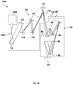
- FIG. 1A shows a schematic view of an EUV lithography apparatus 100A, which comprises a beam shaping and illumination system 102 and a projection system 104.
- EUV stands for "extreme ultraviolet” and denotes a wavelength of the operating light of between 0.1 and 30 nm.
- the beam shaping and illumination system 102 and the projection system 104 are provided in each case in a vacuum housing (not shown), wherein each vacuum housing is evacuated with the aid of an evacuation device (not illustrated).
- the vacuum housings are surrounded by a machine room (not illustrated), in which the drive devices for mechanically moving or setting the optical elements are provided. Electrical controllers and the like may also be furthermore provided in this machine room.
- the EUV lithography apparatus 100A comprises an EUV light source 106A.
- a plasma source or a synchrotron that emits radiation 108A in the EUV range (extreme ultraviolet range), that is to say e.g. in the wavelength range of 5 nm to 20 nm, can be provided as the EUV light source 106A.
- the EUV radiation 108A is focused and the desired operating wavelength is filtered out from the EUV radiation 108A.
- the EUV radiation 108A generated by the EUV light source 106A has a relatively low transmissivity through air, for which reason the beam guiding spaces in the beam shaping and illumination system 102 and in the projection system 104 are evacuated.
- the beam shaping and illumination system 102 illustrated in Figure 1A has five mirrors 110, 112, 114, 116, 118.
- the EUV radiation 108A is guided onto a photomask (called: reticle) 120.
- the photomask 120 is likewise formed as a reflective optical element and may be arranged outside the systems 102, 104.
- the EUV radiation 108A can be directed onto the photomask 120 by means of a mirror 122.
- the photomask 120 has a structure which is imaged onto a wafer 124 or the like in a reduced fashion by means of the projection system 104.
- the projection system 104 (also referred to as projection lens) comprises six mirrors M1 to M6 for imaging the photomask 120 onto the wafer 124.
- individual mirrors M1 to M6 of the projection system 104 can be arranged symmetrically with respect to an optical axis 126 of the projection system 104.
- the number of mirrors of the EUV lithography system 100A is not restricted to the number illustrated. A greater or lesser number of mirrors may also be provided.
- the mirrors are generally curved at their front side for the purpose of beam shaping.
- FIG. 1B shows a schematic view of a DUV lithography apparatus 100B, which comprises a beam shaping and illumination system 102 and a projection system 104.
- DUV stands for "deep ultraviolet” and denotes a wavelength of the operating light of between 30 and 250 nm.
- the beam shaping and illumination system 102 and the projection system 104 can - as already described with reference to Figure 1A , be arranged in a vacuum housing, and/or be surrounded by a machine room with corresponding drive devices.
- the DUV lithography apparatus 100B comprises a DUV light source 106B.
- a DUV light source 106B an ArF excimer laser that emits radiation 108B in the DUV range at 193 nm, for example, can be provided as the DUV light source 106B.
- the beam shaping and illumination system 102 illustrated in Figure 1B guides the DUV radiation 108B onto a photomask 120.
- the photomask 120 is embodied as a transmissive optical element and can be arranged outside the systems 102, 104.
- the photomask 120 has a structure which is imaged onto a wafer 124 or the like in a reduced fashion by means of the projection system 104.
- the projection system 104 has a plurality of lens elements 128 and/or mirrors 130 for imaging the photomask 120 onto the wafer 124.
- individual lens elements 128 and/or mirrors 130 of the projection system 104 may be arranged symmetrically in relation to the optical axis 126 of the projection system 104.
- the number of lens elements and mirrors of the DUV lithography system 100B is not restricted to the number illustrated. A greater or lesser number of lens elements and/or mirrors may also be provided.
- the mirrors are generally curved at their front side for the purpose of beam shaping.
- An air gap between the last lens element 128 and the wafer 124 can be replaced by a liquid medium 132 having a refractive index of > 1.
- the liquid medium can be high-purity water, for example.
- Such a construction is also referred to as immersion lithography and has an increased photolithographic resolution.
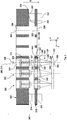
- FIG. 2 shows a schematic plan view of one embodiment of an optical device 200 for the lithography apparatus 100A, 100B.
- the optical device 200 is preferably a facet mirror.
- the facet mirror is designated hereinafter by the reference sign 200.
- the facet mirror 200 can be part of the beam shaping and illumination system 102 or of the projection system 104.
- the mirrors 110, 112, 114, 116, 118 or M1 to M6 can be embodied in each case as one such facet mirror 200.
- the facet mirror 200 comprises a multiplicity of facets 202 arranged linearly.
- the facets 202 are curved arcuately or in a sickle-shaped fashion.
- the facets 202 can also be polygonal, for example hexagonal.
- Figure 2 shows only a small number of facets 202.
- the facet mirror 200 can comprise several hundred to several thousand facets 202. Each facet 202 is tiltable.
- each facet 202 has an optically effective surface 204.
- the optically effective surface 204 is configured for example to reflect EUV radiation 108A or DUV radiation 108B.
- the facet mirror 200 comprises a plurality of drive devices 300.
- Each facet 202 is assigned one of the drive devices 300, with the aid of which the respective facet 202 can be tilted.
- the drive device 300 can also be designated as a motor.
- Perforations 304 are provided in an actuator plate 302 of the facet mirror 200.
- the perforations 304 can be embodied as circular holes penetrating through the actuator plate 302.
- the perforations 304 can also have a geometry deviating from a circular shape in cross section.
- Each perforation 304 comprises a centre axis or axis of symmetry 306, with respect to which the perforation 304 is constructed symmetrically, in particular rotationally symmetrically.
- the axis of symmetry 306 of the perforation 304 is simultaneously a centre axis or axis of symmetry of the drive device 300.
- An electromagnetic actuator 308, in particular a Lorentz actuator, of the drive device 300 is arranged in the perforation 304.
- the electromagnetic actuator 308 can have a plurality of coils, for example four thereof, which are energizable separately from one another.
- the electromagnetic actuator 308 is embodied rotationally symmetrically with respect to a centre axis or axis of symmetry 310.
- the coils are arranged in a manner distributed uniformly around the axis of symmetry 310.
- the respective axis of symmetry 310 can be aligned coaxially with respect to the axis of symmetry 306 of the drive device 300. Coaxially should be understood to mean that the axis of symmetry 306 corresponds to the axis of symmetry 310.
- the electromagnetic actuator 308 is secured in the perforation 304 with the aid of a securing ring 312.
- Interfaces 314, 316 are provided on the actuator plate 302.
- the number of interfaces 314, 316 is arbitrary.
- the interfaces 314, 316 can be embodied for example as fitting pins or fitting springs.
- the perforations 304 are positioned relative to the interfaces 314, 316, or vice-versa. That is to say that the position of each axis of symmetry 306 of each perforation 304 with respect to the interfaces 314, 316 in a first spatial direction x and in a second spatial direction y, different from the first spatial direction x, is known and lies within tolerances governed by production engineering.
- the facet mirror 200 furthermore comprises a carrier plate 318, which is arranged below the actuator plate 302 with respect to a gravitational force direction g.
- the carrier plate 318 can also be arranged above the actuator plate 302 with respect to the gravitational force direction g.
- the carrier plate 318 likewise comprises interfaces 320, 322.
- the interfaces 320, 322 of the carrier plate 318 correspond to the interfaces 314, 316 of the actuator plate 302. That is to say that the interfaces 320, 322 engage into the interfaces 314, 316, or vice-versa.
- the number of interfaces 320, 322 is arbitrary.
- the number of interfaces 314, 316 of the actuator plate 302 corresponds to the number of interfaces 320, 322 of the carrier plate 318.
- the actuator plate 302 and the carrier plate 318 can be positioned relative to one another with respect to the first spatial direction x, the second spatial direction y and a third spatial direction z, which differs from the first spatial direction x and the second spatial direction y. That is to say that the interfaces 320, 322 serve on the carrier plate 318 as a reference for the positioning of components of the drive device 300 that are provided on the carrier plate 318 relative to the actuator plate 302 or relative to the electromagnetic actuator 308 or the axis of symmetry 306.
- the first spatial direction x can also be referred to as the x-axis
- the second spatial direction y can also be referred to as the y-axis
- the third spatial direction can also be referred to as the z-axis.
- the carrier plate 318 has a multiplicity of perforations 324, wherein each drive device 300 is assigned a perforation 324.
- the perforations 324 can be embodied as circular holes. However, the perforations 324 can also have a different geometry in cross section.
- Each perforation 324 is assigned a centre axis or axis of symmetry 325. Ideally, in each drive device 300, the axes of symmetry 306, 310, 325 are positioned coaxially with respect to one another.
- Each drive device 300 furthermore comprises a magnet element 326.
- the magnet element 326 is preferably embodied as a permanent magnet.
- the magnet element 326 comprises at least one magnetic north pole and at least one magnetic south pole.
- the magnet element 326 comprises a centre axis or axis of symmetry 327, with respect to which the magnet element 326 is constructed symmetrically, in particular rotationally symmetrically.
- the magnet element 326 is disc-shaped and can have a circular geometry. Alternatively, the magnet element 326 can also have a different geometry.
- the axis of symmetry 327 is ideally arranged coaxially with respect to the axes of symmetry 306, 310, 325.
- the magnet element 326 is connected to a drive plunger 328.
- the magnet element 326 can be connected to the drive plunger 328 in a positively locking manner.
- a positively locking connection arises as a result of at least two connection partners engaging in or behind one another.
- the magnet element 326 is screwed or clipped to the drive plunger 328. As a result, the magnet element 326 can easily be separated from the drive plunger 328 and reconnected thereto.
- the facet 202 is provided at one end of the drive plunger 328.
- the facet 202 can be connected to the drive plunger 328 in a positively locking manner or cohesively.
- cohesive connections the connection partners are held together by atomic or molecular forces.
- Cohesive connections are non-releasable connections that can be separated only by destruction of the connection means.
- the facet 202 is adhesively bonded to the drive plunger 328.
- the magnet element 326 is arranged at an end of the drive plunger 328 facing away from the facet 202.
- the magnet element 326 is thus coupled to the facet 202 with the aid of the drive plunger 328.
- the drive plunger 328 is led in the form of a rod and centrally through the perforation 324 of the carrier plate 318.
- the drive plunger 328 can have a centre axis or axis of symmetry 330.
- the axis of symmetry 330 is ideally aligned coaxially with respect to the axes of symmetry 306, 310, 325, 327.
- the magnet element 326 is arranged for example between the actuator plate 302 and the carrier plate 318.
- the facet 202 is positioned below the carrier plate 318 with respect to the gravitational force direction g.
- the facet 202 is suspended from or supported on the carrier plate 318 with the aid of restoring springs 332, 334, in particular in the form of flexures.
- the number of restoring springs 332, 334 per facet 202 is arbitrary. By way of example, it is possible to provide two, three, four or even more restoring springs 332, 334 per facet 202.
- the restoring springs 332, 334 are fixedly connected to the facet 202 or to the drive plunger 328 on the facet side. A cohesive or positively locking connection can be provided.
- a securing ring 336 can be provided for this purpose.
- the restoring springs 332, 334 are fixedly connected to the securing ring 336.
- the securing ring 336 has a central perforation 338, through which the drive plunger 328 is led.
- a spacer plate 340 can be provided between the securing ring 336 and the carrier plate 318.
- the securing ring 336 is provided on a front side 342 of the carrier plate 318. The front side 342 faces away from the actuator plate 302.
- the drive device 300 has a magnetic amplification ring 346.
- the amplification ring 346 serves for magnetic field amplification.
- the amplification ring 346 can also be designated as back iron ring (BIR).
- BIR back iron ring
- the amplification ring 346 has a central perforation 348, through which the drive plunger 328 is led.
- the perforation 348 can be circular or preferably oval.
- the amplification ring 346 is aligned centrally with respect to the perforation 324. That is to say that the amplification ring 346 is positioned such that a centre axis or axis of symmetry 349 thereof is arranged coaxially with respect to the axis of symmetry 325.
- the amplification ring 346 can be screwed into the perforation 324.
- the facet 202 can be tilted with the aid of the drive device 300.
- the facet 202 can be tilted about the first spatial direction x and about the second spatial direction y from a zero position NP shown in Figure 3 with the aid of the drive device 300 by corresponding energization of the coils of the electromagnetic actuator 308.
- the facet 202 is restored to the zero position NP with the aid of the restoring springs 332, 334.
- the zero position NP which can also be referred to as mechanical zero position NP as delimitation from an optical zero position of the optically effective surface 204 of the facet 202
- the drive device 300 is aligned symmetrically.
- the mechanical zero position NP can also be referred to as mechanical zero location, mechanical neutral location, mechanical neutral position or mechanically defined position.
- the facets 202 are tilted with the aid of the respective drive device 300.
- What is crucial for the functionality of the drive device 300 is the deflection, that is to say an angular range by which the drive plunger 328 can be tilted.
- the adjusting force of the drive device 300 is restricted.
- the adjusting force to be expended is proportional to the attained angular range of the drive plunger 328. That is to say that the greater the deflection of the drive plunger 328, the greater the adjusting force. The greater the deflection of the drive plunger 328, the greater the current required for energizing the coils of the electromagnetic actuator 308. This can result in severe heating of the electromagnetic actuator 308.
- the constituents of the drive device 300 namely the facet 202, the actuator plate 302, the carrier plate 318, the electromagnetic actuator 308, the magnet element 326, the drive plunger 328 and the amplification ring 346, can actually never be optimally aligned with respect to one another, or can be so aligned only with a very great technical complexity.
- a resulting asymmetry of the drive device 300 has the effect that even when the magnet element 326 is aligned coaxially with respect to the electromagnetic actuator 308, the optical zero position of the facet 202, in which an actual beam offset IA corresponds to a setpoint beam offset SA, is not attained.
- the drive plunger 328 in order to attain the optical zero position, the drive plunger 328 must already be deflected, as a result of which the magnet element 326 is no longer centred centrally in the drive device 300.
- the magnet element 326 is deflected from the mechanical zero position NP in order to attain the optical zero position.
- This effect additionally increases the adjusting force to be applied by the drive device 300, or reduces the angular range by which the drive plunger 328 can be tilted for a given adjusting force.
- the actual beam offset IA deviates from the setpoint beam offset SA of the optically defective surface 204 of the facet 202.
- a light beam L of, for example, visible light is directed onto the optically effective surface 204 of the facet 202 and is reflected therefrom in the direction of a detection device 400.
- the detection device 400 can comprise for example a ground-glass screen and/or an electronic chip.
- a CMOS or CCD chip can be used as the electronic chip.
- the actual beam offset IA can appear as a light point, particularly with the use of a ground-glass screen.
- the setpoint beam offset SA is then correspondingly a reference point, in particular on the ground-glass screen.
- the actual beam offset can deviate from the setpoint beam offset SA both in the first spatial direction x and in the second spatial direction y respectively by a deviation ⁇ x, ⁇ y.
- the actual beam offset IA corresponds to the setpoint beam offset SA or the deviation of the actual beam offset IA from the setpoint beam offset SA lies in a predetermined tolerance range.
- the optically effective surface 204 of the facet 202 is then situated in its optical zero position.
- the predetermined tolerance range can be 50 ⁇ m, for example, both for the first spatial direction x and for the second spatial direction y.
- the facet 202 coupled to the drive plunger 328 In order to reduce the deviation of the actual beam offset IA from the setpoint beam offset SA, it is possible, as already mentioned above, for the facet 202 coupled to the drive plunger 328 to be tilted into the optical zero position with the aid of the drive device 300. In order to attain the optical zero position, the magnet element 326 is displaced out of its central mechanical zero position NP. As a result, firstly, the angular range that the drive device 300 can move to is reduced and, secondly, already in the optical zero position an adjusting force is to be applied to the magnet element 326 with the aid of the electromagnetic actuator 308.
- a method for adjusting the optical device 200 or the drive device 300 of the facet 202 is proposed.
- the amplification ring 346 is removed and the magnet element 326 is positioned in the mechanical zero position NP with the aid of a sleeve-shaped tool 500.
- the magnet element is fixed with respect to the carrier plate 318, in particular with respect to one of the perforations 324, or with respect to the interface 320.
- the magnet element 326 is fixed in all three spatial directions x, y, z.
- the axis of symmetry 327 of the magnet element 326 is positioned coaxially with respect to the axis of symmetry 325 of the perforation 324.
- the amplification ring 346 it is also possible for the amplification ring 346 not to be demounted.
- the tool 500 is configured to position and fix the magnet element 326 relative to the amplification ring 346.
- the axis of symmetry 325 of the perforation 324 is aligned with respect to the interfaces 320, 322, or the position of the axis of symmetry 325 relative to the interfaces 320, 322 with respect to the first spatial direction x and the second spatial direction y is known and the position of the electromagnetic actuator 308 with respect to the interfaces 314, 316 is defined, it suffices to fix the magnet element 326 relative to the carrier plate 318 or relative to the perforation 324 with the aid of the tool 500. That is to say that the magnet element 326 can be aligned symmetrically with respect to the axis of symmetry 325 of the perforation 324 with the aid of the tool 500.
- the deviation of the actual beam offset IA from the setpoint beam offset SA of the optically effective surface 204 is ascertained.
- This ascertaining of the deviation of the actual beam offset IA from the setpoint beam offset SA is carried out with the aid of an optical measurement method.
- the detection device 400 can for example emit the light beam L onto the optically effective surface 204, wherein the light beam L is reflected from the optically effective surface 204 back to the detection device 400.
- the deviation of the actual beam offset IA from the setpoint beam offset SA is ascertained both in the first spatial direction x and in the second spatial direction y.
- the orientation of the magnet element 326 with respect to one of the interfaces 320, 322 is ascertained by means of a tactile measurement method, for example with the aid of a coordinate measuring machine.
- a tactile measurement method for example with the aid of a coordinate measuring machine.
- the tactile measurement method it is possible to detect for example a distance A x in the first spatial direction, a distance A y in the second spatial direction y and/or a distance A z in the third spatial direction z ( Figure 4 and Figure 5 ).
- the distances A x , A y , A z can be ascertained for example between the magnet element 326 and one of the interfaces 320, 322.
- a virtual mounting model for the magnet element 326 is subsequently ascertained. Afterwards, on the basis of said virtual mounting model, the magnet element 326 is influenced such that the deviation of the actual beam offset IA from the setpoint beam offset SA is reduced. In this case, the deviation is reduced to an extent such that predetermined tolerances, for example of a deviation of 50 ⁇ m in each case both in the first spatial direction x and in the second spatial direction y, are complied with. In particular, the magnet element 326 is influenced such that when the optically effective surface 204 of the facet 202 is situated in its optical zero position, the drive device 300 applies no or at least a minimal adjusting force.
- the drive device 300 can be influenced for example by the magnet element 326 being magnetized asymmetrically. As a result, no adjusting force is to be applied in order to attain the optical zero position of the optically effective surface 204 of the facet 202. However, the magnet element 326 is then not necessarily aligned centrally with respect to the electromagnetic actuator 308 in the mechanical zero position NP.
- a geometry, a material, a position and/or an orientation of the amplification ring 346 can be adapted in order to influence the drive device 300. Furthermore, it is also possible to adapt a geometry, a position and/or a tilting of the facet 202 and/or it is possible to adapt a position of the electromagnetic actuator 308 and/or an operating point of the coils of the electromagnetic actuator 308 depending on the deviation ascertained. Furthermore, a stiffness and/or a geometry of the restoring springs 332, 334 can be adapted.
- a position and/or orientation of the magnet element 326 with respect to the optically effective surface 204 are/is adapted such that the actual beam offset IA corresponds to the setpoint beam offset SA or the deviation of the actual beam offset IA from the setpoint beam offset SA lies at least in the predetermined tolerance range.
- the predetermined tolerance range can be for example 50 ⁇ m in each case in the first spatial direction x and in the second spatial direction y.
- the asymmetrical magnetization can also be carried out.
- the position of the magnet element 326 should be understood to mean the coordinates thereof or the coordinates of a measurement point provided on the magnet element 326 with respect to the first spatial direction x, the second spatial direction y and the third spatial direction z.
- the orientation of the magnet element 326 should be understood to mean the tilting thereof with respect to the three spatial directions x, y, z. That is to say that the magnet element 326 can be tilted about the first spatial direction x, the second spatial direction y and/or the third spatial direction z. This results in six degrees of freedom for the positioning and/or orientation of the magnet element 326 with respect to the optically effective surface 204.
- the position and/or orientation of the magnet element 326 with respect to the electromagnetic actuator 308 are/is adapted such that the magnet element 326, with respect to the third spatial direction z, is arranged at a distance a from the electromagnetic actuator 308 that is required for the functionality of the drive device 300.
- the tolerance range to be achieved in the third spatial direction z can be 30 ⁇ m, for example.
- Adapting the position and/or orientation of the magnet element 326 can be carried out for example by a spacer element 350, shown in Figure 6 , being inserted between the drive plunger 328 and the magnet element 326.
- a prefabricated standard blank 352 ( Figure 5 ) is inserted between the magnet element 326 and the drive plunger 328.
- the standard blank 352 can be for example a copper sheet.
- the standard blank 352 is demounted from the drive device 300 and processed in a material-removing manner for example on a machine tool, in particular a CNC machine tool.
- material is mechanically removed from the standard blank 352 in the first spatial direction x, the second spatial direction y and/or the third spatial direction z.
- the standard blank 352 it is also possible to use some other semifinished product for producing the spacer element 350. For example if the standard blank 352 has in the third spatial direction z a thickness that is too small to process said standard blank further in a material-removing manner.
- the spacer element 350 is completed. Afterwards, as shown in Figure 6 , the spacer element 350 is incorporated into the drive device 300 again.
- the processing of the spacer element 350 in the first spatial direction x, the second spatial direction y and/or the third spatial direction z has the effect that when the magnet element 326 is situated in its mechanical zero position NP, that is to say that when the drive device 300 applies a minimal adjusting force, the drive plunger 328 can easily be displaced and/or tilted with respect to the magnet element 326. What is achieved as a result is that the optical zero position of the optically effective surface 204 and the mechanical zero position NP of the magnet element 326 can be attained simultaneously.
- the axis of symmetry 330 of the drive plunger 228 can then be displaced with respect to the axis of symmetry 327 of the magnet element 326 or with respect to the axes of symmetry 306 or 310 in the first spatial direction x and/or in the second spatial direction y, such that the axes of symmetry 327, 330 are no longer positioned coaxially with respect to one another.
- the axis of symmetry 330 can be tilted with respect to the axis of symmetry 327 about the first spatial direction x and/or the second spatial direction y.
- Figure 6 shows a highly exaggerated tilting of the axis of symmetry 330 about the first spatial direction x and a highly exaggerated displacement of the axis of symmetry 330 in the second spatial direction y.
- the magnet element 326 is aligned exactly centrally with respect to the axis of symmetry 310 of the electromagnetic actuator 308 and at the same time the actual beam offset IA corresponds to the setpoint beam offset SA or lies in the predetermined tolerance range. Furthermore, what can be achieved by adapting the standard blank 352 in the third spatial direction z is that the distance a between the magnet element 326 and the electromagnetic actuator 308 assumes a value that is optimal for the functionality of the drive device 300.
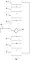
- Figure 7 shows a schematic block diagram of one embodiment of the method for adjusting the optical device 200 or the drive device 300 on the basis of an influencing of the magnet element 326.
- the magnet element 326 is fixed in the mechanical zero position NP.
- the magnet element 326 can be fixed for example with respect to the carrier plate 318, the amplification ring 346 or the interfaces 314, 316, 320, 322.
- Fixing the magnet element 326 is preferably carried out with the actuator plate 302 demounted, wherein the tool 500 centres the magnet element 326 either relative to the perforation 324 or relative to the amplification ring 346.
- the facet 202 is optically measured.
- the deviation of the actual beam offset IA from the setpoint beam offset SA of the optically effective surface 204 of the facet 202 is ascertained. This can be carried out with the aid of the detection device 400.
- the deviation of the actual beam offset IA from the setpoint beam offset SA is ascertained in the first spatial direction x and in the second spatial direction y.
- a step S3 the fixed magnet element 326 is subjected to tactile measurement.
- a coordinate measuring machine can be used for this purpose.
- the deviation in the first spatial direction x, the second spatial direction y and/or the third spatial direction z with respect to the electromagnetic actuator 308 is determined preferably taking account of all the interfaces 314, 316, 320, 322.
- the deviation of the magnet element 326 in the third spatial direction z with respect to the electromagnetic actuator 308 is ascertained in order later to set the optimum distance a.
- a virtual mounting model 600 ( Figure 8 ) for the magnet element 326 is ascertained on the basis of the measurement values ascertained by means of the optical measurement method and the tactile measurement method.
- Step S8 for example the magnet element 326 is influenced in such a way that the deviation of the actual beam offset IA from the setpoint beam offset SA is reduced and at the same time a minimal adjusting force is applied to the magnet element 326 with the aid of the electromagnetic actuator 308.
- Step S8 can be carried out before or after step S7.
- the magnet element 326 is adapted with regard to its position and/or orientation.
- the standard blank 352 is processed by machining for example with the aid of a CNC machine tool, such that the individually adapted spacer element 350 is made available.
- the standard blank 352 can be replaced by a specially manufactured spacer element 350. The standard blank 352 can then be used multiply.
- step S9 the completed spacer element 350 is mounted.
- steps S1 to S9 are repeated until the deviation of the actual beam offset IA from the setpoint beam offset SA is reduced to an extent such that the required tolerances are complied with.
- the optical measurement result detected in step S2, provided with the reference sign OM, and the tactile measurement result detected in step S3, provided with the reference sign TM, are computed regarding the virtual mounting model 600 for providing a computation result VE, on the basis of which step S8 of adjusting is carried out.
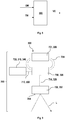
- Figure 9 shows a greatly simplified schematic view of the facet mirror 200, which is referred to hereinafter as optical device 200.
- the optical device 200 comprises a movable component 700.
- the movable component 700 can be a facet 202.
- the optical device 200 furthermore comprises a reference component 702.
- the reference component 702 can be the carrier plate 318, one of the perforations 324 provided in the carrier plate 318, or one of the interfaces 314, 316, 320, 322.
- the movable component 700 is coupled to an optical component 706 with the aid of a mechanical operative connection 704.
- the optical component 706 is preferably a light-reflecting component.
- the optical component 706 can be a facet 202.
- the mechanical operative connection 704 can be the drive plunger 328 or comprise the drive plunger 328.
- the optical device 200 comprises an actuator 707, which can be an electromagnetic actuator 308.
- the actuator 707 can be operatively connected to the movable component 700 with the aid of a field 708, in particular a magnetic field.
- the method shown in Figure 7 is used for adjusting the optical device 200.
- the movable component 700 in step S1, is fixed in a mechanically defined position, in particular in the zero position NP, with respect to the reference component 702.
- the optical component 706 is optically measured in order to obtain the optical measurement result OM.
- the optical device 200 is adjusted depending on the optical measurement result OM.
- step S1 the movable component 700 is fixed relative to the reference component 702 with the aid of a fixing system 710.
- the tool 500 can be provided for this purpose, which tool mechanically fixes the optical component 706 relative to the reference component 702.
- the tool 500 is removed again after step S3 or after step S5.
- Step S2 can comprise detecting the actual beam offset IA, of the optical component 706, wherein the detected actual beam offset IA is compared with the setpoint beam offset SA and adjusting the optical device 200 is carried out depending on the comparison result.
- Adjusting in step S8 can comprise changing a geometry, in particular by mechanical processing, an orientation and/or position, a stiffness, an electric field and/or the magnetic field 708 of at least one component of the optical device 200.
- the at least one component can be the movable component 700, the optical component 706, the magnetic amplification ring 346, the electromagnetic actuator 308 for actuating the movable component 700, the or one of the restoring springs 332, 334 for restoring the movable component 700 and/or such a component which is comprised by the mechanical operative connection 704.
- the drive plunger 328 is comprised by the mechanical operative connection 704.
- the spacer element 350 is inserted between said movable component and the drive plunger 328 of the mechanical operative connection.
- a geometry of the spacer element 350 is preferably adapted in such a way that the orientation and/or the position of the movable component 700 are/is altered.
- the movable component 700 is a magnet element 326, wherein the magnet element 326 is preferably movable with the aid of the electromagnetic actuator 308.
- the reference component 702 is preferably the carrier plate 318, on which the movable component 700 is mounted, and/or the reference component 702 is the magnetic amplification ring 346 for amplifying the magnetic field 708 of the electromagnetic actuator 308.
- the electromagnetic actuator 308 is held by an actuator plate 302, wherein the actuator plate 302 is preferably positioned relative to the carrier plate 318 with the aid of the interfaces 314, 316, 320, 322.
- the optical device 200 is subjected to tactile measurement, wherein, in step S8, as shown in Figure 8 , the optical device 200 is adjusted depending on the optical measurement result OM and the tactile measurement result TM.
- the method also comprises computing the optical measurement result OM and the tactile measurement result TM in the virtual mounting model 600 in order to obtain the computation result VE, wherein the optical device 200 is adjusted depending on the computation result VE in step S8.
- the tactile measurement can also comprise detecting the distance A x , A y , A z between two components of the optical device 200, in particular between the movable component 700 and the reference component 702 and/or between the movable component 700 and at least one of the interfaces 314, 316, 320, 322.
- the optical measurement in step S2 is carried out in the first spatial direction x and in the second spatial direction y, which is orthogonal to the first spatial direction x, wherein the tactile measurement is carried out at least in the third spatial direction z, which is orthogonal to the first and second spatial directions x, y, wherein the tactile measurement is preferably carried out additionally in the first and second spatial directions x, y.
- the method can comprise the steps of optically measuring S2 the optical device 200 in order to obtain an optical measurement result OM, subjecting the optical device 200 to tactile measurement S3 in order to obtain a tactile measurement result TM, and adjusting S8 the optical device 200 depending on the optical measurement result OM and the tactile measurement result TM.
Landscapes
- Physics & Mathematics (AREA)
- General Physics & Mathematics (AREA)
- Engineering & Computer Science (AREA)
- Optics & Photonics (AREA)
- Health & Medical Sciences (AREA)
- Environmental & Geological Engineering (AREA)
- Epidemiology (AREA)
- Public Health (AREA)
- Plasma & Fusion (AREA)
- Exposure And Positioning Against Photoresist Photosensitive Materials (AREA)
- Exposure Of Semiconductors, Excluding Electron Or Ion Beam Exposure (AREA)
Applications Claiming Priority (1)
| Application Number | Priority Date | Filing Date | Title |
|---|---|---|---|
| DE102016212853.1A DE102016212853B3 (de) | 2016-07-14 | 2016-07-14 | Verfahren zum Justieren einer optischen Einrichtung |
Publications (2)
| Publication Number | Publication Date |
|---|---|
| EP3330762A1 true EP3330762A1 (fr) | 2018-06-06 |
| EP3330762B1 EP3330762B1 (fr) | 2019-05-22 |
Family
ID=59315515
Family Applications (1)
| Application Number | Title | Priority Date | Filing Date |
|---|---|---|---|
| EP17180813.2A Active EP3330762B1 (fr) | 2016-07-14 | 2017-07-11 | Procédé de réglage d'un dispositif optique |
Country Status (5)
| Country | Link |
|---|---|
| EP (1) | EP3330762B1 (fr) |
| KR (1) | KR102414479B1 (fr) |
| CN (1) | CN107621756B (fr) |
| DE (1) | DE102016212853B3 (fr) |
| TW (1) | TWI747923B (fr) |
Cited By (6)
| Publication number | Priority date | Publication date | Assignee | Title |
|---|---|---|---|---|
| CN109814254A (zh) * | 2019-03-29 | 2019-05-28 | 李胜保 | 一种激光扫描振镜装置及扫描镜的摆动方法 |
| CN113168105A (zh) * | 2018-10-23 | 2021-07-23 | 卡尔蔡司Smt有限责任公司 | 通过可调节间隔件将光刻设备的第一元件朝向光刻设备的第二元件调整的方法 |
| CN113467378A (zh) * | 2021-07-15 | 2021-10-01 | 苏州谋迅智能科技有限公司 | Cnc时间轴对正的方法 |
| CN114746812A (zh) * | 2019-12-05 | 2022-07-12 | 卡尔蔡司Smt有限责任公司 | 用于安装光学系统的方法 |
| US20230161266A1 (en) * | 2021-11-23 | 2023-05-25 | Carl Zeiss Smt Gmbh | Method of assembling a facet mirror of an optical system |
| US12164102B2 (en) | 2019-05-13 | 2024-12-10 | Carl Zeiss Smt Gmbh | Method for generating a mathematical model for positioning individual mirrors of a facet mirror in an optical system |
Families Citing this family (3)
| Publication number | Priority date | Publication date | Assignee | Title |
|---|---|---|---|---|
| DE102018205714A1 (de) * | 2018-04-16 | 2019-10-17 | Carl Zeiss Smt Gmbh | Verfahren, messsystem und lithographieanlage |
| DE102018130290A1 (de) * | 2018-11-29 | 2020-06-04 | Asml Netherlands B.V. | Aktuatoreinrichtung und Projektionsbelichtungsanlage |
| DE102019202868A1 (de) * | 2019-03-04 | 2020-09-10 | Carl Zeiss Smt Gmbh | Aktuatoreinrichtung und Verfahren zur Ausrichtung eines optischen Elements, optische Baugruppe sowie Projektionsbelichtungsanlage |
Citations (7)
| Publication number | Priority date | Publication date | Assignee | Title |
|---|---|---|---|---|
| US20050111067A1 (en) * | 2003-01-24 | 2005-05-26 | Andreas Seifert | Method for the production of a facetted mirror |
| US20100134859A1 (en) * | 2007-08-06 | 2010-06-03 | Stephen Hastings | Method and apparatus for construction of modular galvano motor scanning heads |
| US20100205793A1 (en) * | 2009-02-16 | 2010-08-19 | Samsung Electronics Co., Ltd. | Lens assembly alignement device for camera lens module |
| DE102012223034A1 (de) | 2012-12-13 | 2013-12-12 | Carl Zeiss Smt Gmbh | Beleuchtungssystem einer Mikrolithographischen Projektionsbelichtungsanlage |
| WO2014060169A1 (fr) | 2012-10-15 | 2014-04-24 | Asml Netherlands B.V. | Mécanisme d'actionnement, appareil optique, appareil de lithographie et procédé de fabrication de dispositifs |
| DE102014216075A1 (de) | 2014-08-13 | 2015-10-15 | Carl Zeiss Smt Gmbh | Spiegelanordnung und optisches System mit einer solchen Spiegelanordnung |
| US20150300807A1 (en) * | 2007-02-06 | 2015-10-22 | Carl Zeiss Smt Gmbh | Method and device for monitoring multiple mirror arrays in an illumination system of a microlithographic projection exposure apparatus |
Family Cites Families (10)
| Publication number | Priority date | Publication date | Assignee | Title |
|---|---|---|---|---|
| JP3989656B2 (ja) * | 1999-10-08 | 2007-10-10 | 松下電器産業株式会社 | 光学ユニットの調整方法、光学ユニットの調整装置 |
| DE10136388A1 (de) * | 2001-07-26 | 2003-02-13 | Zeiss Carl | System zum Vermessen eines optischen Systems, insbesondere eines Objektives |
| JP2006349942A (ja) * | 2005-06-15 | 2006-12-28 | Tamron Co Ltd | 像振れ補正装置及びそれを備えた撮像装置 |
| US7598688B2 (en) * | 2006-06-22 | 2009-10-06 | Orbotech Ltd | Tilting device |
| WO2010037575A1 (fr) * | 2008-09-30 | 2010-04-08 | Asml Netherlands B.V. | Système de projection et appareil lithographique |
| JP5294804B2 (ja) * | 2008-10-31 | 2013-09-18 | 三菱電機株式会社 | 光学調整装置 |
| WO2012126954A1 (fr) * | 2011-03-23 | 2012-09-27 | Carl Zeiss Smt Gmbh | Dispositif de miroir pour uv extrême, système optique comprenant un dispositif de miroir pour uv extrême, et procédé de mise en œuvre d'un dispositif de miroir pour uv extrême |
| JP5960806B2 (ja) * | 2011-06-21 | 2016-08-02 | カール・ツァイス・エスエムティー・ゲーエムベーハー | ファセットミラーデバイス |
| DE102012209412A1 (de) * | 2012-06-04 | 2013-12-05 | Carl Zeiss Smt Gmbh | Optisches Verfahren und optische Messvorrichtung zum Messen von Winkellagen von Facetten zumindest eines Facettenspiegels für EUV-Anwendungen |
| DE102013004738A1 (de) * | 2013-03-12 | 2014-10-02 | Fraunhofer-Gesellschaft zur Förderung der angewandten Forschung e.V. | Verfahren zur zielgerichteten Justierung von optischen Bauelementen zu einer Bezugsachse |
-
2016
- 2016-07-14 DE DE102016212853.1A patent/DE102016212853B3/de active Active
-
2017
- 2017-07-11 EP EP17180813.2A patent/EP3330762B1/fr active Active
- 2017-07-13 TW TW106123491A patent/TWI747923B/zh active
- 2017-07-13 CN CN201710604021.8A patent/CN107621756B/zh active Active
- 2017-07-13 KR KR1020170088964A patent/KR102414479B1/ko active Active
Patent Citations (7)
| Publication number | Priority date | Publication date | Assignee | Title |
|---|---|---|---|---|
| US20050111067A1 (en) * | 2003-01-24 | 2005-05-26 | Andreas Seifert | Method for the production of a facetted mirror |
| US20150300807A1 (en) * | 2007-02-06 | 2015-10-22 | Carl Zeiss Smt Gmbh | Method and device for monitoring multiple mirror arrays in an illumination system of a microlithographic projection exposure apparatus |
| US20100134859A1 (en) * | 2007-08-06 | 2010-06-03 | Stephen Hastings | Method and apparatus for construction of modular galvano motor scanning heads |
| US20100205793A1 (en) * | 2009-02-16 | 2010-08-19 | Samsung Electronics Co., Ltd. | Lens assembly alignement device for camera lens module |
| WO2014060169A1 (fr) | 2012-10-15 | 2014-04-24 | Asml Netherlands B.V. | Mécanisme d'actionnement, appareil optique, appareil de lithographie et procédé de fabrication de dispositifs |
| DE102012223034A1 (de) | 2012-12-13 | 2013-12-12 | Carl Zeiss Smt Gmbh | Beleuchtungssystem einer Mikrolithographischen Projektionsbelichtungsanlage |
| DE102014216075A1 (de) | 2014-08-13 | 2015-10-15 | Carl Zeiss Smt Gmbh | Spiegelanordnung und optisches System mit einer solchen Spiegelanordnung |
Cited By (11)
| Publication number | Priority date | Publication date | Assignee | Title |
|---|---|---|---|---|
| CN113168105A (zh) * | 2018-10-23 | 2021-07-23 | 卡尔蔡司Smt有限责任公司 | 通过可调节间隔件将光刻设备的第一元件朝向光刻设备的第二元件调整的方法 |
| CN113168105B (zh) * | 2018-10-23 | 2024-09-03 | 卡尔蔡司Smt有限责任公司 | 将光刻设备的第一元件朝向第二元件调整的方法 |
| CN109814254A (zh) * | 2019-03-29 | 2019-05-28 | 李胜保 | 一种激光扫描振镜装置及扫描镜的摆动方法 |
| US12164102B2 (en) | 2019-05-13 | 2024-12-10 | Carl Zeiss Smt Gmbh | Method for generating a mathematical model for positioning individual mirrors of a facet mirror in an optical system |
| CN114746812A (zh) * | 2019-12-05 | 2022-07-12 | 卡尔蔡司Smt有限责任公司 | 用于安装光学系统的方法 |
| JP2023504280A (ja) * | 2019-12-05 | 2023-02-02 | カール・ツァイス・エスエムティー・ゲーエムベーハー | 光学系を装着する方法 |
| JP2025094081A (ja) * | 2019-12-05 | 2025-06-24 | カール・ツァイス・エスエムティー・ゲーエムベーハー | 光学系を装着する方法 |
| CN113467378A (zh) * | 2021-07-15 | 2021-10-01 | 苏州谋迅智能科技有限公司 | Cnc时间轴对正的方法 |
| CN113467378B (zh) * | 2021-07-15 | 2024-03-29 | 苏州谋迅智能科技有限公司 | Cnc时间轴对正的方法 |
| US20230161266A1 (en) * | 2021-11-23 | 2023-05-25 | Carl Zeiss Smt Gmbh | Method of assembling a facet mirror of an optical system |
| US11841620B2 (en) * | 2021-11-23 | 2023-12-12 | Carl Zeiss Smt Gmbh | Method of assembling a facet mirror of an optical system |
Also Published As
| Publication number | Publication date |
|---|---|
| KR102414479B1 (ko) | 2022-06-30 |
| TW201809797A (zh) | 2018-03-16 |
| TWI747923B (zh) | 2021-12-01 |
| CN107621756B (zh) | 2021-11-09 |
| KR20180008316A (ko) | 2018-01-24 |
| EP3330762B1 (fr) | 2019-05-22 |
| CN107621756A (zh) | 2018-01-23 |
| DE102016212853B3 (de) | 2017-11-09 |
Similar Documents
| Publication | Publication Date | Title |
|---|---|---|
| EP3330762B1 (fr) | Procédé de réglage d'un dispositif optique | |
| US7125128B2 (en) | Adaptive-optics actuator arrays and methods for using such arrays | |
| JP6862543B2 (ja) | モータアセンブリ、リソグラフィ装置、及びデバイス製造方法 | |
| TWI602030B (zh) | 致動機構、光學裝置、微影裝置及元件製造方法 | |
| KR100573671B1 (ko) | 위치결정 디바이스 제조방법, 위치결정 디바이스 및 이를 포함하는 리소그래피 투영장치 | |
| JP2008022034A (ja) | リソグラフィ装置及びデバイス製造方法 | |
| CN105900017A (zh) | 致动机构、光学装置和光刻装置 | |
| US7333180B2 (en) | Positioning apparatus and exposure apparatus using the same | |
| US20080105069A1 (en) | Fine Stage Z Support Apparatus | |
| US7423733B2 (en) | Lithographic apparatus, device manufacturing method, and device manufactured thereby with docking system for positioning a patterning device | |
| US20080029682A1 (en) | Fine stage "Z" support apparatus | |
| EP0973067A2 (fr) | Dispositif de positionnement et appareil de projection lithographique muni d'un tel dispositif | |
| KR102230068B1 (ko) | 마이크로리소그래피 투영 노광 장치의 조립체 | |
| US20250370357A1 (en) | Optical assembly, optical system and projection exposure apparatus | |
| US7283210B2 (en) | Image shift optic for optical system | |
| JP6965332B2 (ja) | 基板ハンドリングシステムおよびリソグラフィ装置 | |
| WO2014136143A1 (fr) | Dispositif mobile, dispositif d'exposition et procédé de fabrication de dispositif | |
| JP2008252149A (ja) | 組立体、リソグラフィ装置及びデバイス製造方法 | |
| EP1335248A1 (fr) | Appareil lithographique et méthode de fabrication d'un dispositif |
Legal Events
| Date | Code | Title | Description |
|---|---|---|---|
| PUAI | Public reference made under article 153(3) epc to a published international application that has entered the european phase |
Free format text: ORIGINAL CODE: 0009012 |
|
| STAA | Information on the status of an ep patent application or granted ep patent |
Free format text: STATUS: THE APPLICATION HAS BEEN PUBLISHED |
|
| AK | Designated contracting states |
Kind code of ref document: A1 Designated state(s): AL AT BE BG CH CY CZ DE DK EE ES FI FR GB GR HR HU IE IS IT LI LT LU LV MC MK MT NL NO PL PT RO RS SE SI SK SM TR |
|
| AX | Request for extension of the european patent |
Extension state: BA ME |
|
| STAA | Information on the status of an ep patent application or granted ep patent |
Free format text: STATUS: REQUEST FOR EXAMINATION WAS MADE |
|
| REG | Reference to a national code |
Ref country code: DE Ref legal event code: R079 Ref document number: 602017004082 Country of ref document: DE Free format text: PREVIOUS MAIN CLASS: G02B0007182000 Ipc: G03F0007200000 |
|
| 17P | Request for examination filed |
Effective date: 20180705 |
|
| RBV | Designated contracting states (corrected) |
Designated state(s): AL AT BE BG CH CY CZ DE DK EE ES FI FR GB GR HR HU IE IS IT LI LT LU LV MC MK MT NL NO PL PT RO RS SE SI SK SM TR |
|
| RIC1 | Information provided on ipc code assigned before grant |
Ipc: G02B 7/182 20060101ALI20180807BHEP Ipc: G03F 7/20 20060101AFI20180807BHEP |
|
| GRAP | Despatch of communication of intention to grant a patent |
Free format text: ORIGINAL CODE: EPIDOSNIGR1 |
|
| STAA | Information on the status of an ep patent application or granted ep patent |
Free format text: STATUS: GRANT OF PATENT IS INTENDED |
|
| INTG | Intention to grant announced |
Effective date: 20181004 |
|
| GRAS | Grant fee paid |
Free format text: ORIGINAL CODE: EPIDOSNIGR3 |
|
| GRAJ | Information related to disapproval of communication of intention to grant by the applicant or resumption of examination proceedings by the epo deleted |
Free format text: ORIGINAL CODE: EPIDOSDIGR1 |
|
| GRAL | Information related to payment of fee for publishing/printing deleted |
Free format text: ORIGINAL CODE: EPIDOSDIGR3 |
|
| STAA | Information on the status of an ep patent application or granted ep patent |
Free format text: STATUS: REQUEST FOR EXAMINATION WAS MADE |
|
| GRAR | Information related to intention to grant a patent recorded |
Free format text: ORIGINAL CODE: EPIDOSNIGR71 |
|
| STAA | Information on the status of an ep patent application or granted ep patent |
Free format text: STATUS: GRANT OF PATENT IS INTENDED |
|
| GRAA | (expected) grant |
Free format text: ORIGINAL CODE: 0009210 |
|
| STAA | Information on the status of an ep patent application or granted ep patent |
Free format text: STATUS: THE PATENT HAS BEEN GRANTED |
|
| INTC | Intention to grant announced (deleted) | ||
| AK | Designated contracting states |
Kind code of ref document: B1 Designated state(s): AL AT BE BG CH CY CZ DE DK EE ES FI FR GB GR HR HU IE IS IT LI LT LU LV MC MK MT NL NO PL PT RO RS SE SI SK SM TR |
|
| INTG | Intention to grant announced |
Effective date: 20190415 |
|
| REG | Reference to a national code |
Ref country code: GB Ref legal event code: FG4D |
|
| REG | Reference to a national code |
Ref country code: CH Ref legal event code: EP |
|
| REG | Reference to a national code |
Ref country code: IE Ref legal event code: FG4D |
|
| REG | Reference to a national code |
Ref country code: AT Ref legal event code: REF Ref document number: 1136833 Country of ref document: AT Kind code of ref document: T Effective date: 20190615 |
|
| REG | Reference to a national code |
Ref country code: DE Ref legal event code: R096 Ref document number: 602017004082 Country of ref document: DE |
|
| REG | Reference to a national code |
Ref country code: NL Ref legal event code: FP |
|
| REG | Reference to a national code |
Ref country code: LT Ref legal event code: MG4D |
|
| PG25 | Lapsed in a contracting state [announced via postgrant information from national office to epo] |
Ref country code: ES Free format text: LAPSE BECAUSE OF FAILURE TO SUBMIT A TRANSLATION OF THE DESCRIPTION OR TO PAY THE FEE WITHIN THE PRESCRIBED TIME-LIMIT Effective date: 20190522 Ref country code: LT Free format text: LAPSE BECAUSE OF FAILURE TO SUBMIT A TRANSLATION OF THE DESCRIPTION OR TO PAY THE FEE WITHIN THE PRESCRIBED TIME-LIMIT Effective date: 20190522 Ref country code: HR Free format text: LAPSE BECAUSE OF FAILURE TO SUBMIT A TRANSLATION OF THE DESCRIPTION OR TO PAY THE FEE WITHIN THE PRESCRIBED TIME-LIMIT Effective date: 20190522 Ref country code: PT Free format text: LAPSE BECAUSE OF FAILURE TO SUBMIT A TRANSLATION OF THE DESCRIPTION OR TO PAY THE FEE WITHIN THE PRESCRIBED TIME-LIMIT Effective date: 20190922 Ref country code: SE Free format text: LAPSE BECAUSE OF FAILURE TO SUBMIT A TRANSLATION OF THE DESCRIPTION OR TO PAY THE FEE WITHIN THE PRESCRIBED TIME-LIMIT Effective date: 20190522 Ref country code: AL Free format text: LAPSE BECAUSE OF FAILURE TO SUBMIT A TRANSLATION OF THE DESCRIPTION OR TO PAY THE FEE WITHIN THE PRESCRIBED TIME-LIMIT Effective date: 20190522 Ref country code: NO Free format text: LAPSE BECAUSE OF FAILURE TO SUBMIT A TRANSLATION OF THE DESCRIPTION OR TO PAY THE FEE WITHIN THE PRESCRIBED TIME-LIMIT Effective date: 20190822 Ref country code: FI Free format text: LAPSE BECAUSE OF FAILURE TO SUBMIT A TRANSLATION OF THE DESCRIPTION OR TO PAY THE FEE WITHIN THE PRESCRIBED TIME-LIMIT Effective date: 20190522 |
|
| PG25 | Lapsed in a contracting state [announced via postgrant information from national office to epo] |
Ref country code: LV Free format text: LAPSE BECAUSE OF FAILURE TO SUBMIT A TRANSLATION OF THE DESCRIPTION OR TO PAY THE FEE WITHIN THE PRESCRIBED TIME-LIMIT Effective date: 20190522 Ref country code: GR Free format text: LAPSE BECAUSE OF FAILURE TO SUBMIT A TRANSLATION OF THE DESCRIPTION OR TO PAY THE FEE WITHIN THE PRESCRIBED TIME-LIMIT Effective date: 20190823 Ref country code: RS Free format text: LAPSE BECAUSE OF FAILURE TO SUBMIT A TRANSLATION OF THE DESCRIPTION OR TO PAY THE FEE WITHIN THE PRESCRIBED TIME-LIMIT Effective date: 20190522 Ref country code: BG Free format text: LAPSE BECAUSE OF FAILURE TO SUBMIT A TRANSLATION OF THE DESCRIPTION OR TO PAY THE FEE WITHIN THE PRESCRIBED TIME-LIMIT Effective date: 20190822 |
|
| REG | Reference to a national code |
Ref country code: AT Ref legal event code: MK05 Ref document number: 1136833 Country of ref document: AT Kind code of ref document: T Effective date: 20190522 |
|
| PG25 | Lapsed in a contracting state [announced via postgrant information from national office to epo] |
Ref country code: EE Free format text: LAPSE BECAUSE OF FAILURE TO SUBMIT A TRANSLATION OF THE DESCRIPTION OR TO PAY THE FEE WITHIN THE PRESCRIBED TIME-LIMIT Effective date: 20190522 Ref country code: AT Free format text: LAPSE BECAUSE OF FAILURE TO SUBMIT A TRANSLATION OF THE DESCRIPTION OR TO PAY THE FEE WITHIN THE PRESCRIBED TIME-LIMIT Effective date: 20190522 Ref country code: DK Free format text: LAPSE BECAUSE OF FAILURE TO SUBMIT A TRANSLATION OF THE DESCRIPTION OR TO PAY THE FEE WITHIN THE PRESCRIBED TIME-LIMIT Effective date: 20190522 Ref country code: CZ Free format text: LAPSE BECAUSE OF FAILURE TO SUBMIT A TRANSLATION OF THE DESCRIPTION OR TO PAY THE FEE WITHIN THE PRESCRIBED TIME-LIMIT Effective date: 20190522 Ref country code: RO Free format text: LAPSE BECAUSE OF FAILURE TO SUBMIT A TRANSLATION OF THE DESCRIPTION OR TO PAY THE FEE WITHIN THE PRESCRIBED TIME-LIMIT Effective date: 20190522 Ref country code: SK Free format text: LAPSE BECAUSE OF FAILURE TO SUBMIT A TRANSLATION OF THE DESCRIPTION OR TO PAY THE FEE WITHIN THE PRESCRIBED TIME-LIMIT Effective date: 20190522 |
|
| REG | Reference to a national code |
Ref country code: DE Ref legal event code: R119 Ref document number: 602017004082 Country of ref document: DE |
|
| PG25 | Lapsed in a contracting state [announced via postgrant information from national office to epo] |
Ref country code: MC Free format text: LAPSE BECAUSE OF FAILURE TO SUBMIT A TRANSLATION OF THE DESCRIPTION OR TO PAY THE FEE WITHIN THE PRESCRIBED TIME-LIMIT Effective date: 20190522 Ref country code: IT Free format text: LAPSE BECAUSE OF FAILURE TO SUBMIT A TRANSLATION OF THE DESCRIPTION OR TO PAY THE FEE WITHIN THE PRESCRIBED TIME-LIMIT Effective date: 20190522 Ref country code: SM Free format text: LAPSE BECAUSE OF FAILURE TO SUBMIT A TRANSLATION OF THE DESCRIPTION OR TO PAY THE FEE WITHIN THE PRESCRIBED TIME-LIMIT Effective date: 20190522 |
|
| PLBE | No opposition filed within time limit |
Free format text: ORIGINAL CODE: 0009261 |
|
| STAA | Information on the status of an ep patent application or granted ep patent |
Free format text: STATUS: NO OPPOSITION FILED WITHIN TIME LIMIT |
|
| PG25 | Lapsed in a contracting state [announced via postgrant information from national office to epo] |
Ref country code: TR Free format text: LAPSE BECAUSE OF FAILURE TO SUBMIT A TRANSLATION OF THE DESCRIPTION OR TO PAY THE FEE WITHIN THE PRESCRIBED TIME-LIMIT Effective date: 20190522 |
|
| REG | Reference to a national code |
Ref country code: BE Ref legal event code: MM Effective date: 20190731 |
|
| 26N | No opposition filed |
Effective date: 20200225 |
|
| PG25 | Lapsed in a contracting state [announced via postgrant information from national office to epo] |
Ref country code: PL Free format text: LAPSE BECAUSE OF FAILURE TO SUBMIT A TRANSLATION OF THE DESCRIPTION OR TO PAY THE FEE WITHIN THE PRESCRIBED TIME-LIMIT Effective date: 20190522 Ref country code: DE Free format text: LAPSE BECAUSE OF NON-PAYMENT OF DUE FEES Effective date: 20200201 |
|
| PG25 | Lapsed in a contracting state [announced via postgrant information from national office to epo] |
Ref country code: LU Free format text: LAPSE BECAUSE OF NON-PAYMENT OF DUE FEES Effective date: 20190711 Ref country code: BE Free format text: LAPSE BECAUSE OF NON-PAYMENT OF DUE FEES Effective date: 20190731 Ref country code: SI Free format text: LAPSE BECAUSE OF FAILURE TO SUBMIT A TRANSLATION OF THE DESCRIPTION OR TO PAY THE FEE WITHIN THE PRESCRIBED TIME-LIMIT Effective date: 20190522 |
|
| PG25 | Lapsed in a contracting state [announced via postgrant information from national office to epo] |
Ref country code: FR Free format text: LAPSE BECAUSE OF NON-PAYMENT OF DUE FEES Effective date: 20190722 |
|
| PG25 | Lapsed in a contracting state [announced via postgrant information from national office to epo] |
Ref country code: IE Free format text: LAPSE BECAUSE OF NON-PAYMENT OF DUE FEES Effective date: 20190711 |
|
| REG | Reference to a national code |
Ref country code: CH Ref legal event code: PL |
|
| PG25 | Lapsed in a contracting state [announced via postgrant information from national office to epo] |
Ref country code: CH Free format text: LAPSE BECAUSE OF NON-PAYMENT OF DUE FEES Effective date: 20200731 Ref country code: LI Free format text: LAPSE BECAUSE OF NON-PAYMENT OF DUE FEES Effective date: 20200731 |
|
| PG25 | Lapsed in a contracting state [announced via postgrant information from national office to epo] |
Ref country code: CY Free format text: LAPSE BECAUSE OF FAILURE TO SUBMIT A TRANSLATION OF THE DESCRIPTION OR TO PAY THE FEE WITHIN THE PRESCRIBED TIME-LIMIT Effective date: 20190522 |
|
| PG25 | Lapsed in a contracting state [announced via postgrant information from national office to epo] |
Ref country code: IS Free format text: LAPSE BECAUSE OF FAILURE TO SUBMIT A TRANSLATION OF THE DESCRIPTION OR TO PAY THE FEE WITHIN THE PRESCRIBED TIME-LIMIT Effective date: 20190922 |
|
| PG25 | Lapsed in a contracting state [announced via postgrant information from national office to epo] |
Ref country code: MT Free format text: LAPSE BECAUSE OF FAILURE TO SUBMIT A TRANSLATION OF THE DESCRIPTION OR TO PAY THE FEE WITHIN THE PRESCRIBED TIME-LIMIT Effective date: 20190522 Ref country code: HU Free format text: LAPSE BECAUSE OF FAILURE TO SUBMIT A TRANSLATION OF THE DESCRIPTION OR TO PAY THE FEE WITHIN THE PRESCRIBED TIME-LIMIT; INVALID AB INITIO Effective date: 20170711 |
|
| GBPC | Gb: european patent ceased through non-payment of renewal fee |
Effective date: 20210711 |
|
| PG25 | Lapsed in a contracting state [announced via postgrant information from national office to epo] |
Ref country code: GB Free format text: LAPSE BECAUSE OF NON-PAYMENT OF DUE FEES Effective date: 20210711 |
|
| PG25 | Lapsed in a contracting state [announced via postgrant information from national office to epo] |
Ref country code: MK Free format text: LAPSE BECAUSE OF FAILURE TO SUBMIT A TRANSLATION OF THE DESCRIPTION OR TO PAY THE FEE WITHIN THE PRESCRIBED TIME-LIMIT Effective date: 20190522 |
|
| P01 | Opt-out of the competence of the unified patent court (upc) registered |
Effective date: 20230525 |
|
| PGFP | Annual fee paid to national office [announced via postgrant information from national office to epo] |
Ref country code: NL Payment date: 20250721 Year of fee payment: 9 |