EP3330829A1 - Compensation de courant de base d'un miroir de courant bjt - Google Patents
Compensation de courant de base d'un miroir de courant bjt Download PDFInfo
- Publication number
- EP3330829A1 EP3330829A1 EP17176566.2A EP17176566A EP3330829A1 EP 3330829 A1 EP3330829 A1 EP 3330829A1 EP 17176566 A EP17176566 A EP 17176566A EP 3330829 A1 EP3330829 A1 EP 3330829A1
- Authority
- EP
- European Patent Office
- Prior art keywords
- bjt
- current
- terminal
- current mirror
- circuit
- Prior art date
- Legal status (The legal status is an assumption and is not a legal conclusion. Google has not performed a legal analysis and makes no representation as to the accuracy of the status listed.)
- Granted
Links
Images

Classifications
-
- G—PHYSICS
- G05—CONTROLLING; REGULATING
- G05F—SYSTEMS FOR REGULATING ELECTRIC OR MAGNETIC VARIABLES
- G05F3/00—Non-retroactive systems for regulating electric variables by using an uncontrolled element, or an uncontrolled combination of elements, such element or such combination having self-regulating properties
- G05F3/02—Regulating voltage or current
- G05F3/08—Regulating voltage or current wherein the variable is DC
- G05F3/10—Regulating voltage or current wherein the variable is DC using uncontrolled devices with non-linear characteristics
- G05F3/16—Regulating voltage or current wherein the variable is DC using uncontrolled devices with non-linear characteristics being semiconductor devices
- G05F3/20—Regulating voltage or current wherein the variable is DC using uncontrolled devices with non-linear characteristics being semiconductor devices using diode- transistor combinations
- G05F3/26—Current mirrors
- G05F3/267—Current mirrors using both bipolar and field-effect technology
Definitions
- the present invention relates to current mirroring circuits and, in particular, to a current mirror circuit using bipolar junction transistors (BJTs) with base current compensation.
- BJTs bipolar junction transistors
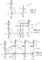
- Figure 1 shows a circuit diagram for a conventional current mirror circuit 10.
- the circuit includes an input current leg 12 and at least one output current leg 14.
- a current source 16 generates an input current Iin that is applied to the input current leg 12.
- the input current Iin is mirrored over to the output current leg 14 where an output current Iout is generated.
- the ratio of the magnitude of the output current to the input current is referred to as the mirroring ratio.
- the circuit 10 is implemented using bipolar junction transistors (BJTs).
- the input current leg 12 includes a first BJT device 20 that is configured as a diode-connected device.
- the collector terminal of the first BJT device 20 is electrically coupled to the base terminal of the first BJT device 20, and the collector terminal of the first BJT device 20 is configured to receive the input current Iin from the current source 16.
- the emitter terminal of the first BJT device 20 is electrically coupled to a reference voltage supply node.
- the reference voltage supply node may comprise a ground (Gnd) voltage node.
- the output current leg 14 includes a second BJT device 22.
- the base terminal of the second BJT device 22 is electrically coupled to the base terminal of the first BJT device 20.
- the emitter terminal of the second BJT device 22 is electrically coupled to the reference voltage supply node.
- the output current Iout in the output current leg 14 is generated at the collector terminal of the second BJT device 22.
- Figure 2 shows a circuit diagram for a conventional current mirror circuit 30.
- the circuit 30 differs from the circuit 10 in that the output current leg 14 includes a plurality of parallel connected second BJT devices 22(1)-22(n) forming a variable output transistor 22v.
- the base terminals of the second BJT devices 22(l)-22(n) are electrically coupled to the base terminal of the first BJT device 20.
- the emitter terminals of the second BJT devices 22(1)-22(n) are electrically coupled to the reference voltage supply node.
- the collector terminals of the second BJT devices 22(l)-22(n) are electrically coupled to a common output current node 32, through respective switches 34(1)-34(n).
- the output current Iout in the output current leg 14 is generated at the common output current node 32 as a sum of the currents generated at the collector terminals of the second BJT devices 22(1)-22(n).
- the magnitude of the output current Iout is accordingly dependent on the number of second BJT devices 22(l)-22(n) that are actuated using the corresponding switches 34(1)-34(n) electrically coupled between the collector terminal and the common output current node 32.
- a multibit digital control signal D can be used to selectively actuate the switches 34(1)-34(n).
- FIG. 3 shows a circuit diagram for a conventional current mirror circuit 50.
- the circuit 50 differs from the circuit 30 in that multiple output current legs 14(1)-14(m) are provided.
- Each output current leg 14(1)-14(m) includes a variable output transistor 22v.
- the base terminals of the variable output transistors 22v(1)-22v(m) are electrically coupled to the base terminal of the first BJT device 20.
- the emitter terminals of the variable output transistors 22v(1)-22v(m) are electrically coupled to the reference voltage supply node.
- Each common output current node 32(1)-32(m) generates a distinct output current Iout(l)-Iout(m) for a corresponding current channel CH(1)-CH(m).
- a current mirror circuit is provided, according to appended claim 1.
- a current mirror circuit comprises an input current leg and an output current leg.
- the input current leg includes: a first bipolar junction transistor (BJT) having a collector terminal configured to receive an input current sourced at a current node; and a first metal oxide semiconductor field effect transistor (MOSFET) having a gate terminal coupled to the current node and a source terminal coupled to a base terminal of the first BJT.
- the output current leg includes: a second BJT having a collector terminal configured to supply an output current; and a second MOSFET having a gate terminal coupled to the current node and a source terminal coupled to a base terminal of the second BJT.
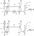
- the circuit 100 includes an input current leg 112 and at least one output current leg 114.
- a current source 116 generates an input current Iin that is applied to the input current leg 112.
- the input current Iin is mirrored over to the output current leg 114 where an output current Iout is generated.
- the ratio of the magnitude of the output current to the input current is referred to as the mirroring ratio.
- the mirroring function of the circuit 100 is implemented using bipolar junction transistors (BJTs).
- the input current leg 112 includes a first BJT device 120.
- the collector terminal of the first BJT device 120 is configured to receive the input current Iin from the current source 116.
- the emitter terminal of the first BJT device 120 is electrically coupled to a reference voltage supply node.
- the reference voltage supply node may comprise a ground (Gnd) voltage node.
- the output current leg 114 includes a second BJT device 122.
- the base terminal of the second BJT device 122 is electrically coupled to the base terminal of the first BJT device 120.
- the emitter terminal of the second BJT device 122 is electrically coupled to the reference voltage supply node.
- the output current Iout in the output current leg 114 is generated at the collector terminal of the second BJT device 122.
- the collector terminal of the first BJT device 120 is electrically coupled to the base terminal of the first BJT device 120 through an n-channel metal oxide semiconductor field effect transistor (MOSFET) device 102.
- MOSFET metal oxide semiconductor field effect transistor
- the gate terminal of MOSFET device 102 is electrically coupled to the collector terminal of the first BJT device 120 at a reference current node 104.
- the source terminal of MOSFET device 102 is electrically coupled to the base terminal of the first BJT device 120.
- the drain terminal of MOSFET device 102 is electrically coupled to a further reference voltage supply node.
- the further reference voltage supply node may comprise a positive (Vdd) voltage node.
- the collector terminal of the first BJT device 120 is further electrically coupled to the base terminal of the second BJT device 122 through an n-channel MOSFET device 106.
- the gate terminal of MOSFET device 106 is electrically coupled to the collector terminal of the first BJT device 120 at the reference current node 104.
- the source terminal of MOSFET device 106 is electrically coupled to the base terminal of the second BJT device 122.
- the drain terminal of MOSFET device 106 is electrically coupled to the further reference voltage supply node.
- Resistor Rp on the transistor common base connection line 108 between the first BJT device 120 and the second BJT device 122 is a parasitic line resistance.
- source terminal of MOSFET device 102 is electrically coupled to the base terminal of the first BJT device 120 on one end of the parasitic line resistance (adjacent to base terminal of the first BJT device 120) while the source terminal of MOSFET device 106 is electrically coupled to the base terminal of the second BJT device 122 on an opposite end of the parasitic line resistance (adjacent to the base terminal of the second BJT device 122).
- This electric line interconnection may extend over a not-insignificant length in the physical circuit layout on substrate.
- a component is considered to be "adjacent" to the BJT device if it is closer in layout to that device than to another BJT device.
- the MOSFET device 102 is adjacent to first BJT device 120 (second BJT device 122 being further away) and MOSFET device 106 is adjacent to second BJT device 122 (first BJT device 120 being further away). So, the "adjacent" MOSFET device would be the MOSFET device that is closest in the physical circuit layout on substrate to the BJT device.
- One or more capacitors C can be coupled between the reference current node 104 and the reference voltage supply node (Gnd).
- one capacitor is provided adjacent to the MOSFET device 102 and another capacitor is provided adjacent to the MOSFET device 106.
- a component is considered to be "adjacent" another component of the circuit if it is closer in layout to that component than to another similar component. So, the adjacent capacitor is the capacitor that is closest in the physical circuit layout on substrate to the MOSFET device.
- FIG. 5 showing a circuit diagram for a current mirror circuit 100'.
- the circuit 100' is substantially similar in design to the circuit 100 of Figure 4 .
- the circuit 100' differs from the circuit 100 in that there is no transistor common base connection line 108. Nonetheless, the MOSFET device 102 and the MOSFET device 106 function to control substantially equal (i.e., same within +/- 2.5%) base voltages for the BJT devices.
- the MOSFET devices 102 and 106 may be physically separated from each other by a not-insignificant distance in the physical circuit layout on substrate.
- the circuit 200 is substantially similar in design to the circuit 100 of Figure 4 .
- the circuit 200 differs from the circuit 100 in that it comprises a plurality of parallel connected output current legs 114(1)-114(n).
- Each output current leg 114(1)-114(n) includes a respective second BJT device 122(1)-122(n); the plurality of second BJT devices 122(1)-122(n) forming a variable output transistor 122v.
- the base terminals of the second BJT devices 122(1)-122(n) are electrically coupled to the base terminal of the first BJT device 120.
- the emitter terminals of the second BJT devices 122(1)-122(n) are electrically coupled to the reference voltage supply node (Gnd).
- the collector terminals of the second BJT devices 122(l)-122(n) are electrically coupled to a common output current node 132.
- the output current Iout is generated at the common output current node 132 as a sum of the currents generated at the collector terminals of the second BJT devices 122(1)-122(n).
- the magnitude of the output current Iout is accordingly dependent on the number of second BJT devices 122(1)-122(n) that are actuated using corresponding switches 134(1)-134(n) electrically coupled between the collector terminal and the common output current node 132.
- a multibit digital control signal D can be used to selectively actuate the switches 134(1)-134(n).
- FIG. 7 showing a circuit diagram for a current mirror circuit 200'.
- the circuit 200' is substantially similar in design to the circuit 200 of Figure 6 .
- the circuit 200' differs from the circuit 200 in that there is no transistor common base connection line 108. Nonetheless, the MOSFET device 102 and the MOSFET device 106 function to control substantially equal (i.e., same within +/- 2.5%) base voltages for the BJT devices.
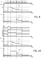
- FIG. 8 showing a waveform diagram illustrating operation of the circuits of Figures 6-7 .
- the voltage at the common output current node 132 is precharged to a desired voltage level Vpre.
- the digital control signal D is set to a first digital value D1.
- a first number of the switches 134(1)-134(n) are actuated.
- the currents flowing through the second BJT devices 122(1)-122(n) in the corresponding actuated output legs 114(1)-114(n) are summed at the common output current node 132 to generate a first magnitude current I1 for the output current Iout.
- the voltage at the common output current node 132 is discharged at a first rate 140.
- the digital control signal D is set to a second digital value D2.
- a second number of the switches 134(1)-134(n) is actuated. So, certain ones of the switches 134 actuated at time t2 are deactuated at time t3.
- the currents flowing through the second BJT devices 122(l)-122(n) in the corresponding actuated output legs 114(1)-114(n) are summed at the common output current node 132 to generate a second magnitude current I2 for the output current Iout that is less than the first magnitude current I1.
- the voltage at the common output current node 132 is discharged at a second rate 142 that is less than the first rate 140.
- the transition in current magnitude at time t3 is not a step function (reference 144).
- the provision of the MOSFET device 102 and the MOSFET device 106 to control substantially equal base voltages for the BJT devices 120 and 122 helps to minimize the charge error produced as a result of switching off one or more of the second BJT devices 122(l)-122(n) at time t3.
- the digital control signal D is set to a third digital value D3.
- the switches 134(1)-134(n) are deactuated and the output current Iout goes to zero.
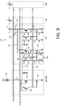
- FIG. 9 showing a circuit diagram for a current mirror circuit 300.
- the circuit 300 is similar in design to the circuit 200 of Figure 6 .
- the circuit 300 differs from the circuit 200 in the following ways:
- the circuit 300 may comprise a plurality of output channels CH1, CH2, ..., CHK.
- Each output channel CH1, CH2, ..., CHK may comprise a plurality of output legs.
- the circuit 300 further includes a second cascode transistor 304;
- second cascode transistor 304 is an n-channel MOSFET whose source-drain path is coupled in series with the collector-emitter path of the second BJT device 122.
- the source terminal of second cascode transistor 304 is electrically coupled to the collector of second BJT transistor 122 and the drain terminal of second cascode transistor 304 is electrically coupled to the common output current node 132.
- the gate terminal of second cascode transistor 304 is driven by a switching circuit 306.
- the switching circuit 306 includes a first switch selectively actuated in response to signal A to couple the gate terminal of second cascode transistor 304 to the cascode bias voltage Vcascode and a second switch selectively actuated in response to signal B to couple the gate and source terminals of second cascode transistor 304 to each other.
- the first cascode transistor 302 functions to set the same collector to emitter voltage across the BJT device 120 as collector to emitter voltage across the second BJT device 122 set by second cascode transistor 304.
- the second cascode device 304 functions to increase output impedance of the current mirror which leads to lower sensitivity of the output current Iout on the current mirror output voltage Vout.
- each output leg includes a switching circuit 308 to drive the gate terminal of MOSFET device 106.
- the switching circuit 308 includes a first switch selectively actuated in response to signal A to couple the gate terminal of MOSFET device 106 to the reference current node 104 and a second switch selectively actuated in response to signal B to couple the gate and source terminals of MOSFET device 106 to each other.
- signal B When signal B is asserted and the second switch is turned on, the gate-to-source voltage Vgs of MOSFET device 106 is zero and the MOSFET device 106 is effectively turned off.
- each output leg includes a switching circuit 310 to drive the base terminal of second BJT device 122.
- the switching circuit 310 includes a first switch selectively actuated in response to signal A to couple the base terminal of second BJT device 122 to the common base connection line 108, a second switch selectively actuated in response to signal B to couple the base and emitter terminals of second BJT device 122 to each other at ground, and a third switch selectively actuated in response to signal B to couple the collector terminal of second BJT device 122 to ground.
- signal B is asserted and the second and third switches are turned on, the base-to-emitter voltage Vbe of second BJT device 122 is zero, the collector is grounded, and the device is effectively turned off.
- Each channel CH1-CHK also includes a switching circuit 314 comprising a switch to selectively couple the common output current node 132 to a precharge voltage Vpre.
- the switch of switching circuit 314 is selectively actuated in response to signal E.
- Each channel CH1-CHK further includes a switching circuit 316 comprising a switch to selectively couple to the common output current node 132 for current output.
- the switch of switching circuit 316 is selectively actuated in response to signal F.
- each output current channel CH may include a plurality of parallel connected second BJT devices 122 forming the variable output transistor 122v.
- two second BJT devices 122a and 122b are provided.
- the control signals A and B for the switching circuits 306, 308 and 310 use a suffix identification (a or b) corresponding to the second BJT device 122a or 122b to which the switching circuits 306, 308 and 310 are coupled.
- the control signals Aa and Ba control switches associated with the operation of the second BJT device 122a while control signals Ab and Bb control switches associated with the operation the second BJT device 122b.
- FIG. 10 showing a waveform diagram illustrating operation of the circuits of Figure 9 .
- the signals Aa and Ab are deasserted and the signals Ba and Bb are asserted.
- the transistors 106, 122 and 304 are turned off.
- signal E is asserted with a pulse to actuate switching circuit 314 and the voltage at the common output current node 132 is precharged to a desired voltage level Vpre.
- the signals Aa and Ab are asserted and the signals Ba and Bb are deasserted to enable operation of the transistors 106, 122 and 304.
- the signals Aa/Ba and Ab/Bb are non-overlapping control signals to ensure that at no time are the switches simultaneously enabled.
- the signal F is asserted to actuate switching circuit 316.
- both second BJT devices 122a and 122b are enabled, the currents flowing through the second BJT devices 122a and 122b are summed at the common output current node 132 to generate a first magnitude current I1 for the output current Iout.
- the voltage at the common output current node 132 is discharged at a first rate 140.
- the signal Ab is deasserted and the signal Bb is asserted.
- the second BJT device 122b is according disabled and its corresponding current is no longer supplied to the common output current node 132 and a second magnitude current I2 is generated for the output current Iout that is less than the first magnitude current I1.
- the voltage at the common output current node 132 is discharged at a second rate 142 that is less than the first rate 140.
- the signal Aa is deasserted and the signal Ba is asserted.
- the second BJT device 122a is according disabled and its corresponding current is no longer supplied to the common output current node 132.
- the signal F is also deaserted.
- the output current Iout accordingly goes to zero.
- the output voltage also falls at time t4.
- output current node 132 becomes a high impedance node and the voltage at that node is not well defined. Rather, the voltage is mainly defined by actual circuit behavior in a fast transient condition. Charge injection of all components play a role there, but the final voltage on output current node 132 is not particularly important because switching circuit 316 is turned off. The voltage Vout is affected by the capacitive external circuitry and thus the voltage will not drop all the way to zero.
- the current mirror circuit can include a plurality of output current channels.
- the implementation of Figure 9 shows K such output channels (CH1-CHK). Each output channel would have a same or similar circuit configuration as shown in detail with respect to channel CH1.
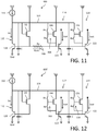
- FIG. 11 showing a circuit diagram for a current mirror circuit 400.
- the circuit 400 is substantially similar in design to the circuit 100 of Figure 4 .
- the circuit 400 differs from the circuit 100 in that it includes the switching circuit 308 for driving the gate terminal of the MOSFET device 106 of each output channel, each channel having here one output current leg 114.
- the configuration and operation of the switching 308 is described in detail in connection with Figure 9 .
- FIG. 12 showing a circuit diagram for a current mirror circuit 400'.
- the circuit 400' is substantially similar in design to the circuit 400 of Figure 11 .
- the circuit 400' differs from the circuit 400 in that there is no transistor common base connection line 108. Nonetheless, the MOSFET device 102 and the MOSFET device 106 function to control substantially equal (i.e., same within +/- 2.5%) base voltages for the BJT devices.
Landscapes
- Engineering & Computer Science (AREA)
- Physics & Mathematics (AREA)
- Microelectronics & Electronic Packaging (AREA)
- Nonlinear Science (AREA)
- Electromagnetism (AREA)
- General Physics & Mathematics (AREA)
- Radar, Positioning & Navigation (AREA)
- Automation & Control Theory (AREA)
- Control Of Electrical Variables (AREA)
- Amplifiers (AREA)
- Electronic Switches (AREA)
Applications Claiming Priority (1)
| Application Number | Priority Date | Filing Date | Title |
|---|---|---|---|
| US15/367,628 US9864395B1 (en) | 2016-12-02 | 2016-12-02 | Base current compensation for a BJT current mirror |
Publications (2)
| Publication Number | Publication Date |
|---|---|
| EP3330829A1 true EP3330829A1 (fr) | 2018-06-06 |
| EP3330829B1 EP3330829B1 (fr) | 2019-12-25 |
Family
ID=59093400
Family Applications (1)
| Application Number | Title | Priority Date | Filing Date |
|---|---|---|---|
| EP17176566.2A Active EP3330829B1 (fr) | 2016-12-02 | 2017-06-19 | Compensation de courant de base d'un miroir de courant bjt |
Country Status (3)
| Country | Link |
|---|---|
| US (1) | US9864395B1 (fr) |
| EP (1) | EP3330829B1 (fr) |
| CN (2) | CN108153371B (fr) |
Families Citing this family (6)
| Publication number | Priority date | Publication date | Assignee | Title |
|---|---|---|---|---|
| US9864395B1 (en) * | 2016-12-02 | 2018-01-09 | Stmicroelectronics Asia Pacific Pte Ltd | Base current compensation for a BJT current mirror |
| US10642303B1 (en) * | 2019-03-14 | 2020-05-05 | Nxp Usa, Inc. | Fast-enable current source |
| US11394337B2 (en) * | 2020-07-01 | 2022-07-19 | Whirlpool Corporation | Method and circuit for soft starting a mixer |
| CN112230702B (zh) * | 2020-11-03 | 2025-05-27 | 成都明夷电子科技股份有限公司 | 一种SiGe工艺信号放大器尾电流偏置电路 |
| CN116048187B (zh) * | 2023-01-09 | 2026-03-06 | 光梓信息科技(深圳)有限公司 | 一种电流镜电路及电流源 |
| CN117908611B (zh) * | 2024-01-11 | 2025-11-25 | 电子科技大学 | 一种用于ldo的bjt输入级的基极电流补偿电路 |
Citations (3)
| Publication number | Priority date | Publication date | Assignee | Title |
|---|---|---|---|---|
| FR2469038A1 (fr) * | 1979-11-05 | 1981-05-08 | Sony Corp | Circuit miroir de courant |
| US5684394A (en) * | 1994-06-28 | 1997-11-04 | Texas Instruments Incorporated | Beta helper for voltage and current reference circuits |
| US7081797B1 (en) * | 2004-12-22 | 2006-07-25 | Analog Devices, Inc. | Multiplying current mirror with base current compensation |
Family Cites Families (6)
| Publication number | Priority date | Publication date | Assignee | Title |
|---|---|---|---|---|
| US4853610A (en) * | 1988-12-05 | 1989-08-01 | Harris Semiconductor Patents, Inc. | Precision temperature-stable current sources/sinks |
| JP4817825B2 (ja) * | 2005-12-08 | 2011-11-16 | エルピーダメモリ株式会社 | 基準電圧発生回路 |
| US8228052B2 (en) * | 2009-03-31 | 2012-07-24 | Analog Devices, Inc. | Method and circuit for low power voltage reference and bias current generator |
| US9523994B2 (en) | 2014-03-07 | 2016-12-20 | Stmicroelectronics Asia Pacific Pte Ltd | Temperature insensitive transient current source |
| US9563223B2 (en) * | 2015-05-19 | 2017-02-07 | Avago Technologies General Ip (Singapore) Pte. Ltd. | Low-voltage current mirror circuit and method |
| US9864395B1 (en) * | 2016-12-02 | 2018-01-09 | Stmicroelectronics Asia Pacific Pte Ltd | Base current compensation for a BJT current mirror |
-
2016
- 2016-12-02 US US15/367,628 patent/US9864395B1/en active Active
-
2017
- 2017-05-31 CN CN201710399144.2A patent/CN108153371B/zh active Active
- 2017-05-31 CN CN201720623366.3U patent/CN207301852U/zh active Active
- 2017-06-19 EP EP17176566.2A patent/EP3330829B1/fr active Active
Patent Citations (3)
| Publication number | Priority date | Publication date | Assignee | Title |
|---|---|---|---|---|
| FR2469038A1 (fr) * | 1979-11-05 | 1981-05-08 | Sony Corp | Circuit miroir de courant |
| US5684394A (en) * | 1994-06-28 | 1997-11-04 | Texas Instruments Incorporated | Beta helper for voltage and current reference circuits |
| US7081797B1 (en) * | 2004-12-22 | 2006-07-25 | Analog Devices, Inc. | Multiplying current mirror with base current compensation |
Non-Patent Citations (1)
| Title |
|---|
| WIKI: "Chapter 11: The Current Mirror", 9 January 2014 (2014-01-09), XP002777774, Retrieved from the Internet <URL:https://wiki.analog.com/university/courses/electronics/text/chapter-11?rev=1389286868> [retrieved on 20180130] * |
Also Published As
| Publication number | Publication date |
|---|---|
| CN207301852U (zh) | 2018-05-01 |
| CN108153371A (zh) | 2018-06-12 |
| US9864395B1 (en) | 2018-01-09 |
| EP3330829B1 (fr) | 2019-12-25 |
| CN108153371B (zh) | 2021-05-11 |
Similar Documents
| Publication | Publication Date | Title |
|---|---|---|
| EP3330829B1 (fr) | Compensation de courant de base d'un miroir de courant bjt | |
| US8604862B2 (en) | Four-quadrant bootstrapped switch circuit | |
| CN108075737B (zh) | 用于驱动电容性负载的低输出阻抗、高速高压电压生成器 | |
| US9081404B2 (en) | Voltage regulator having input stage and current mirror | |
| CN104181371B (zh) | 电路布置 | |
| US20200400785A1 (en) | Low voltage sub-nanosecond pulsed current driver ic for high-resolution lidar applications | |
| US20070296392A1 (en) | Bandgap reference circuits | |
| US10020739B2 (en) | Integrated current replicator and method of operating the same | |
| US20080265860A1 (en) | Low voltage bandgap reference source | |
| CN112882524B (zh) | 带隙基准电路、对应的设备和方法 | |
| KR101783484B1 (ko) | 가변 저항 회로를 구비한 반도체 집적 회로 | |
| US20070115741A1 (en) | Current Sensing Circuit and Boost Converter Having the Same | |
| US9448575B2 (en) | Bipolar transistor adjustable shunt regulator circuit | |
| JP2020030179A (ja) | 電流検出回路 | |
| US6784720B2 (en) | Current switching circuit | |
| CN113341192A (zh) | 电流检测电路 | |
| US11489519B2 (en) | Analog switch with boost current for fast turn on | |
| US4973857A (en) | Current divider circuit | |
| CN113434005A (zh) | 一种可控电阻电路 | |
| US20070177323A1 (en) | High voltage switch using low voltage cmos transistors | |
| CN117220657A (zh) | 高压开关电路及芯片 | |
| US11502674B2 (en) | Optimized low Ron flatness gate driver | |
| CN115940902A (zh) | 一种开关电路 | |
| EP1213636A2 (fr) | Circuit miroir de courant | |
| US4814635A (en) | Voltage translator circuit |
Legal Events
| Date | Code | Title | Description |
|---|---|---|---|
| PUAI | Public reference made under article 153(3) epc to a published international application that has entered the european phase |
Free format text: ORIGINAL CODE: 0009012 |
|
| STAA | Information on the status of an ep patent application or granted ep patent |
Free format text: STATUS: THE APPLICATION HAS BEEN PUBLISHED |
|
| AK | Designated contracting states |
Kind code of ref document: A1 Designated state(s): AL AT BE BG CH CY CZ DE DK EE ES FI FR GB GR HR HU IE IS IT LI LT LU LV MC MK MT NL NO PL PT RO RS SE SI SK SM TR |
|
| AX | Request for extension of the european patent |
Extension state: BA ME |
|
| STAA | Information on the status of an ep patent application or granted ep patent |
Free format text: STATUS: REQUEST FOR EXAMINATION WAS MADE |
|
| 17P | Request for examination filed |
Effective date: 20181203 |
|
| RBV | Designated contracting states (corrected) |
Designated state(s): AL AT BE BG CH CY CZ DE DK EE ES FI FR GB GR HR HU IE IS IT LI LT LU LV MC MK MT NL NO PL PT RO RS SE SI SK SM TR |
|
| GRAP | Despatch of communication of intention to grant a patent |
Free format text: ORIGINAL CODE: EPIDOSNIGR1 |
|
| STAA | Information on the status of an ep patent application or granted ep patent |
Free format text: STATUS: GRANT OF PATENT IS INTENDED |
|
| INTG | Intention to grant announced |
Effective date: 20190702 |
|
| GRAS | Grant fee paid |
Free format text: ORIGINAL CODE: EPIDOSNIGR3 |
|
| GRAA | (expected) grant |
Free format text: ORIGINAL CODE: 0009210 |
|
| STAA | Information on the status of an ep patent application or granted ep patent |
Free format text: STATUS: THE PATENT HAS BEEN GRANTED |
|
| AK | Designated contracting states |
Kind code of ref document: B1 Designated state(s): AL AT BE BG CH CY CZ DE DK EE ES FI FR GB GR HR HU IE IS IT LI LT LU LV MC MK MT NL NO PL PT RO RS SE SI SK SM TR |
|
| REG | Reference to a national code |
Ref country code: GB Ref legal event code: FG4D |
|
| REG | Reference to a national code |
Ref country code: CH Ref legal event code: EP |
|
| REG | Reference to a national code |
Ref country code: AT Ref legal event code: REF Ref document number: 1217823 Country of ref document: AT Kind code of ref document: T Effective date: 20200115 |
|
| REG | Reference to a national code |
Ref country code: DE Ref legal event code: R096 Ref document number: 602017010016 Country of ref document: DE |
|
| REG | Reference to a national code |
Ref country code: IE Ref legal event code: FG4D |
|
| REG | Reference to a national code |
Ref country code: NL Ref legal event code: MP Effective date: 20191225 |
|
| PG25 | Lapsed in a contracting state [announced via postgrant information from national office to epo] |
Ref country code: LV Free format text: LAPSE BECAUSE OF FAILURE TO SUBMIT A TRANSLATION OF THE DESCRIPTION OR TO PAY THE FEE WITHIN THE PRESCRIBED TIME-LIMIT Effective date: 20191225 Ref country code: SE Free format text: LAPSE BECAUSE OF FAILURE TO SUBMIT A TRANSLATION OF THE DESCRIPTION OR TO PAY THE FEE WITHIN THE PRESCRIBED TIME-LIMIT Effective date: 20191225 Ref country code: LT Free format text: LAPSE BECAUSE OF FAILURE TO SUBMIT A TRANSLATION OF THE DESCRIPTION OR TO PAY THE FEE WITHIN THE PRESCRIBED TIME-LIMIT Effective date: 20191225 Ref country code: GR Free format text: LAPSE BECAUSE OF FAILURE TO SUBMIT A TRANSLATION OF THE DESCRIPTION OR TO PAY THE FEE WITHIN THE PRESCRIBED TIME-LIMIT Effective date: 20200326 Ref country code: NO Free format text: LAPSE BECAUSE OF FAILURE TO SUBMIT A TRANSLATION OF THE DESCRIPTION OR TO PAY THE FEE WITHIN THE PRESCRIBED TIME-LIMIT Effective date: 20200325 Ref country code: BG Free format text: LAPSE BECAUSE OF FAILURE TO SUBMIT A TRANSLATION OF THE DESCRIPTION OR TO PAY THE FEE WITHIN THE PRESCRIBED TIME-LIMIT Effective date: 20200325 Ref country code: FI Free format text: LAPSE BECAUSE OF FAILURE TO SUBMIT A TRANSLATION OF THE DESCRIPTION OR TO PAY THE FEE WITHIN THE PRESCRIBED TIME-LIMIT Effective date: 20191225 |
|
| REG | Reference to a national code |
Ref country code: LT Ref legal event code: MG4D |
|
| PG25 | Lapsed in a contracting state [announced via postgrant information from national office to epo] |
Ref country code: HR Free format text: LAPSE BECAUSE OF FAILURE TO SUBMIT A TRANSLATION OF THE DESCRIPTION OR TO PAY THE FEE WITHIN THE PRESCRIBED TIME-LIMIT Effective date: 20191225 Ref country code: RS Free format text: LAPSE BECAUSE OF FAILURE TO SUBMIT A TRANSLATION OF THE DESCRIPTION OR TO PAY THE FEE WITHIN THE PRESCRIBED TIME-LIMIT Effective date: 20191225 |
|
| PG25 | Lapsed in a contracting state [announced via postgrant information from national office to epo] |
Ref country code: AL Free format text: LAPSE BECAUSE OF FAILURE TO SUBMIT A TRANSLATION OF THE DESCRIPTION OR TO PAY THE FEE WITHIN THE PRESCRIBED TIME-LIMIT Effective date: 20191225 |
|
| PG25 | Lapsed in a contracting state [announced via postgrant information from national office to epo] |
Ref country code: RO Free format text: LAPSE BECAUSE OF FAILURE TO SUBMIT A TRANSLATION OF THE DESCRIPTION OR TO PAY THE FEE WITHIN THE PRESCRIBED TIME-LIMIT Effective date: 20191225 Ref country code: CZ Free format text: LAPSE BECAUSE OF FAILURE TO SUBMIT A TRANSLATION OF THE DESCRIPTION OR TO PAY THE FEE WITHIN THE PRESCRIBED TIME-LIMIT Effective date: 20191225 Ref country code: NL Free format text: LAPSE BECAUSE OF FAILURE TO SUBMIT A TRANSLATION OF THE DESCRIPTION OR TO PAY THE FEE WITHIN THE PRESCRIBED TIME-LIMIT Effective date: 20191225 Ref country code: PT Free format text: LAPSE BECAUSE OF FAILURE TO SUBMIT A TRANSLATION OF THE DESCRIPTION OR TO PAY THE FEE WITHIN THE PRESCRIBED TIME-LIMIT Effective date: 20200520 Ref country code: EE Free format text: LAPSE BECAUSE OF FAILURE TO SUBMIT A TRANSLATION OF THE DESCRIPTION OR TO PAY THE FEE WITHIN THE PRESCRIBED TIME-LIMIT Effective date: 20191225 |
|
| PG25 | Lapsed in a contracting state [announced via postgrant information from national office to epo] |
Ref country code: IS Free format text: LAPSE BECAUSE OF FAILURE TO SUBMIT A TRANSLATION OF THE DESCRIPTION OR TO PAY THE FEE WITHIN THE PRESCRIBED TIME-LIMIT Effective date: 20200425 Ref country code: SK Free format text: LAPSE BECAUSE OF FAILURE TO SUBMIT A TRANSLATION OF THE DESCRIPTION OR TO PAY THE FEE WITHIN THE PRESCRIBED TIME-LIMIT Effective date: 20191225 Ref country code: SM Free format text: LAPSE BECAUSE OF FAILURE TO SUBMIT A TRANSLATION OF THE DESCRIPTION OR TO PAY THE FEE WITHIN THE PRESCRIBED TIME-LIMIT Effective date: 20191225 |
|
| REG | Reference to a national code |
Ref country code: DE Ref legal event code: R097 Ref document number: 602017010016 Country of ref document: DE |
|
| PG25 | Lapsed in a contracting state [announced via postgrant information from national office to epo] |
Ref country code: ES Free format text: LAPSE BECAUSE OF FAILURE TO SUBMIT A TRANSLATION OF THE DESCRIPTION OR TO PAY THE FEE WITHIN THE PRESCRIBED TIME-LIMIT Effective date: 20191225 Ref country code: DK Free format text: LAPSE BECAUSE OF FAILURE TO SUBMIT A TRANSLATION OF THE DESCRIPTION OR TO PAY THE FEE WITHIN THE PRESCRIBED TIME-LIMIT Effective date: 20191225 |
|
| PLBE | No opposition filed within time limit |
Free format text: ORIGINAL CODE: 0009261 |
|
| STAA | Information on the status of an ep patent application or granted ep patent |
Free format text: STATUS: NO OPPOSITION FILED WITHIN TIME LIMIT |
|
| REG | Reference to a national code |
Ref country code: AT Ref legal event code: MK05 Ref document number: 1217823 Country of ref document: AT Kind code of ref document: T Effective date: 20191225 |
|
| PG25 | Lapsed in a contracting state [announced via postgrant information from national office to epo] |
Ref country code: SI Free format text: LAPSE BECAUSE OF FAILURE TO SUBMIT A TRANSLATION OF THE DESCRIPTION OR TO PAY THE FEE WITHIN THE PRESCRIBED TIME-LIMIT Effective date: 20191225 |
|
| 26N | No opposition filed |
Effective date: 20200928 |
|
| PG25 | Lapsed in a contracting state [announced via postgrant information from national office to epo] |
Ref country code: MC Free format text: LAPSE BECAUSE OF FAILURE TO SUBMIT A TRANSLATION OF THE DESCRIPTION OR TO PAY THE FEE WITHIN THE PRESCRIBED TIME-LIMIT Effective date: 20191225 Ref country code: AT Free format text: LAPSE BECAUSE OF FAILURE TO SUBMIT A TRANSLATION OF THE DESCRIPTION OR TO PAY THE FEE WITHIN THE PRESCRIBED TIME-LIMIT Effective date: 20191225 Ref country code: IT Free format text: LAPSE BECAUSE OF FAILURE TO SUBMIT A TRANSLATION OF THE DESCRIPTION OR TO PAY THE FEE WITHIN THE PRESCRIBED TIME-LIMIT Effective date: 20191225 |
|
| REG | Reference to a national code |
Ref country code: CH Ref legal event code: PL |
|
| PG25 | Lapsed in a contracting state [announced via postgrant information from national office to epo] |
Ref country code: PL Free format text: LAPSE BECAUSE OF FAILURE TO SUBMIT A TRANSLATION OF THE DESCRIPTION OR TO PAY THE FEE WITHIN THE PRESCRIBED TIME-LIMIT Effective date: 20191225 |
|
| PG25 | Lapsed in a contracting state [announced via postgrant information from national office to epo] |
Ref country code: LU Free format text: LAPSE BECAUSE OF NON-PAYMENT OF DUE FEES Effective date: 20200619 |
|
| REG | Reference to a national code |
Ref country code: BE Ref legal event code: MM Effective date: 20200630 |
|
| PG25 | Lapsed in a contracting state [announced via postgrant information from national office to epo] |
Ref country code: LI Free format text: LAPSE BECAUSE OF NON-PAYMENT OF DUE FEES Effective date: 20200630 Ref country code: CH Free format text: LAPSE BECAUSE OF NON-PAYMENT OF DUE FEES Effective date: 20200630 Ref country code: IE Free format text: LAPSE BECAUSE OF NON-PAYMENT OF DUE FEES Effective date: 20200619 Ref country code: FR Free format text: LAPSE BECAUSE OF NON-PAYMENT OF DUE FEES Effective date: 20200630 |
|
| PG25 | Lapsed in a contracting state [announced via postgrant information from national office to epo] |
Ref country code: BE Free format text: LAPSE BECAUSE OF NON-PAYMENT OF DUE FEES Effective date: 20200630 |
|
| GBPC | Gb: european patent ceased through non-payment of renewal fee |
Effective date: 20210619 |
|
| PG25 | Lapsed in a contracting state [announced via postgrant information from national office to epo] |
Ref country code: GB Free format text: LAPSE BECAUSE OF NON-PAYMENT OF DUE FEES Effective date: 20210619 |
|
| PG25 | Lapsed in a contracting state [announced via postgrant information from national office to epo] |
Ref country code: TR Free format text: LAPSE BECAUSE OF FAILURE TO SUBMIT A TRANSLATION OF THE DESCRIPTION OR TO PAY THE FEE WITHIN THE PRESCRIBED TIME-LIMIT Effective date: 20191225 Ref country code: MT Free format text: LAPSE BECAUSE OF FAILURE TO SUBMIT A TRANSLATION OF THE DESCRIPTION OR TO PAY THE FEE WITHIN THE PRESCRIBED TIME-LIMIT Effective date: 20191225 Ref country code: CY Free format text: LAPSE BECAUSE OF FAILURE TO SUBMIT A TRANSLATION OF THE DESCRIPTION OR TO PAY THE FEE WITHIN THE PRESCRIBED TIME-LIMIT Effective date: 20191225 |
|
| PG25 | Lapsed in a contracting state [announced via postgrant information from national office to epo] |
Ref country code: MK Free format text: LAPSE BECAUSE OF FAILURE TO SUBMIT A TRANSLATION OF THE DESCRIPTION OR TO PAY THE FEE WITHIN THE PRESCRIBED TIME-LIMIT Effective date: 20191225 |
|
| REG | Reference to a national code |
Ref country code: DE Ref legal event code: R081 Ref document number: 602017010016 Country of ref document: DE Owner name: STMICROELECTRONICS INTERNATIONAL N.V., CH Free format text: FORMER OWNERS: STMICROELECTRONICS ASIA PACIFIC PTE LTD., SINGAPORE, SG; STMICROELECTRONICS DESIGN AND APPLICATION S.R.O., PRAHA, CZ |
|
| PGFP | Annual fee paid to national office [announced via postgrant information from national office to epo] |
Ref country code: DE Payment date: 20250520 Year of fee payment: 9 |