EP3330896B1 - Manipulationsdetektor - Google Patents
Manipulationsdetektor Download PDFInfo
- Publication number
- EP3330896B1 EP3330896B1 EP17204847.2A EP17204847A EP3330896B1 EP 3330896 B1 EP3330896 B1 EP 3330896B1 EP 17204847 A EP17204847 A EP 17204847A EP 3330896 B1 EP3330896 B1 EP 3330896B1
- Authority
- EP
- European Patent Office
- Prior art keywords
- detection
- status
- detection element
- oscillator
- circuit
- Prior art date
- Legal status (The legal status is an assumption and is not a legal conclusion. Google has not performed a legal analysis and makes no representation as to the accuracy of the status listed.)
- Active
Links
Images




Classifications
-
- G—PHYSICS
- G01—MEASURING; TESTING
- G01R—MEASURING ELECTRIC VARIABLES; MEASURING MAGNETIC VARIABLES
- G01R27/00—Arrangements for measuring resistance, reactance, impedance, or electric characteristics derived therefrom
- G01R27/28—Measuring attenuation, gain, phase shift or derived characteristics of electric four pole networks, i.e. two-port networks; Measuring transient response
-
- G—PHYSICS
- G06—COMPUTING OR CALCULATING; COUNTING
- G06K—GRAPHICAL DATA READING; PRESENTATION OF DATA; RECORD CARRIERS; HANDLING RECORD CARRIERS
- G06K19/00—Record carriers for use with machines and with at least a part designed to carry digital markings
- G06K19/06—Record carriers for use with machines and with at least a part designed to carry digital markings characterised by the kind of the digital marking, e.g. shape, nature, code
- G06K19/067—Record carriers with conductive marks, printed circuits or semiconductor circuit elements, e.g. credit or identity cards also with resonating or responding marks without active components
- G06K19/07—Record carriers with conductive marks, printed circuits or semiconductor circuit elements, e.g. credit or identity cards also with resonating or responding marks without active components with integrated circuit chips
- G06K19/0701—Record carriers with conductive marks, printed circuits or semiconductor circuit elements, e.g. credit or identity cards also with resonating or responding marks without active components with integrated circuit chips at least one of the integrated circuit chips comprising an arrangement for power management
- G06K19/0707—Record carriers with conductive marks, printed circuits or semiconductor circuit elements, e.g. credit or identity cards also with resonating or responding marks without active components with integrated circuit chips at least one of the integrated circuit chips comprising an arrangement for power management the arrangement being capable of collecting energy from external energy sources, e.g. thermocouples, vibration, electromagnetic radiation
- G06K19/0708—Record carriers with conductive marks, printed circuits or semiconductor circuit elements, e.g. credit or identity cards also with resonating or responding marks without active components with integrated circuit chips at least one of the integrated circuit chips comprising an arrangement for power management the arrangement being capable of collecting energy from external energy sources, e.g. thermocouples, vibration, electromagnetic radiation the source being electromagnetic or magnetic
- G06K19/0709—Record carriers with conductive marks, printed circuits or semiconductor circuit elements, e.g. credit or identity cards also with resonating or responding marks without active components with integrated circuit chips at least one of the integrated circuit chips comprising an arrangement for power management the arrangement being capable of collecting energy from external energy sources, e.g. thermocouples, vibration, electromagnetic radiation the source being electromagnetic or magnetic the source being an interrogation field
-
- G—PHYSICS
- G01—MEASURING; TESTING
- G01N—INVESTIGATING OR ANALYSING MATERIALS BY DETERMINING THEIR CHEMICAL OR PHYSICAL PROPERTIES
- G01N27/00—Investigating or analysing materials by the use of electric, electrochemical, or magnetic means
- G01N27/02—Investigating or analysing materials by the use of electric, electrochemical, or magnetic means by investigating impedance
-
- G—PHYSICS
- G06—COMPUTING OR CALCULATING; COUNTING
- G06K—GRAPHICAL DATA READING; PRESENTATION OF DATA; RECORD CARRIERS; HANDLING RECORD CARRIERS
- G06K19/00—Record carriers for use with machines and with at least a part designed to carry digital markings
- G06K19/06—Record carriers for use with machines and with at least a part designed to carry digital markings characterised by the kind of the digital marking, e.g. shape, nature, code
- G06K19/067—Record carriers with conductive marks, printed circuits or semiconductor circuit elements, e.g. credit or identity cards also with resonating or responding marks without active components
- G06K19/07—Record carriers with conductive marks, printed circuits or semiconductor circuit elements, e.g. credit or identity cards also with resonating or responding marks without active components with integrated circuit chips
- G06K19/0716—Record carriers with conductive marks, printed circuits or semiconductor circuit elements, e.g. credit or identity cards also with resonating or responding marks without active components with integrated circuit chips at least one of the integrated circuit chips comprising a sensor or an interface to a sensor
-
- G—PHYSICS
- G06—COMPUTING OR CALCULATING; COUNTING
- G06K—GRAPHICAL DATA READING; PRESENTATION OF DATA; RECORD CARRIERS; HANDLING RECORD CARRIERS
- G06K19/00—Record carriers for use with machines and with at least a part designed to carry digital markings
- G06K19/06—Record carriers for use with machines and with at least a part designed to carry digital markings characterised by the kind of the digital marking, e.g. shape, nature, code
- G06K19/067—Record carriers with conductive marks, printed circuits or semiconductor circuit elements, e.g. credit or identity cards also with resonating or responding marks without active components
- G06K19/07—Record carriers with conductive marks, printed circuits or semiconductor circuit elements, e.g. credit or identity cards also with resonating or responding marks without active components with integrated circuit chips
- G06K19/0723—Record carriers with conductive marks, printed circuits or semiconductor circuit elements, e.g. credit or identity cards also with resonating or responding marks without active components with integrated circuit chips the record carrier comprising an arrangement for non-contact communication, e.g. wireless communication circuits on transponder cards, non-contact smart cards or RFIDs
-
- G—PHYSICS
- G06—COMPUTING OR CALCULATING; COUNTING
- G06K—GRAPHICAL DATA READING; PRESENTATION OF DATA; RECORD CARRIERS; HANDLING RECORD CARRIERS
- G06K19/00—Record carriers for use with machines and with at least a part designed to carry digital markings
- G06K19/06—Record carriers for use with machines and with at least a part designed to carry digital markings characterised by the kind of the digital marking, e.g. shape, nature, code
- G06K19/067—Record carriers with conductive marks, printed circuits or semiconductor circuit elements, e.g. credit or identity cards also with resonating or responding marks without active components
- G06K19/07—Record carriers with conductive marks, printed circuits or semiconductor circuit elements, e.g. credit or identity cards also with resonating or responding marks without active components with integrated circuit chips
- G06K19/077—Constructional details, e.g. mounting of circuits in the carrier
- G06K19/07749—Constructional details, e.g. mounting of circuits in the carrier the record carrier being capable of non-contact communication, e.g. constructional details of the antenna of a non-contact smart card
- G06K19/07798—Constructional details, e.g. mounting of circuits in the carrier the record carrier being capable of non-contact communication, e.g. constructional details of the antenna of a non-contact smart card part of the antenna or the integrated circuit being adapted for rupturing or breaking, e.g. record carriers functioning as sealing devices for detecting not-authenticated opening of containers
Definitions
- the present specification relates to systems, methods, apparatuses, devices, articles of manufacture and instructions for tamper detection.
- US 2012/218110 discloses an apparatus, system and method for forming RFID labels.
- US 2007/069875 discloses a tamper monitor circuit that detects voltage, temperature, and/or clock variations that may be associated with a circuit tampering technique, and triggers an appropriate tamper response.
- EP 2876581 discloses an apparatus, method and package for electronic tamper detection.
- a tamper detection device comprising: detection circuit, configured to be powered by a near-field-communication (NFC) signal and store a status of a detection element; wherein the detection circuit is configured to set the status to undisturbed in response to an undisturbed state of the detection element; wherein the detection circuit is configured to set the status to disturbed in response to a disturbed state of the detection element; and wherein the detection circuit is configured to electrically report the detection element status in response to a wireless query signal.
- NFC near-field-communication
- the detection circuit is configured to continue to operate and electrically report the detection element status even after the detection element has been placed in the disturbed state.
- the detection circuit is configured so that, once the status is set to disturbed, the status cannot afterwards be reset to undisturbed.
- the detection circuit includes a reference oscillator and a detection oscillator; the detection circuit is configured to count a number of detection oscillator clock cycles and compare to a number of reference oscillator clock cycles; and the detection circuit sets the detection element status to the disturbed status if the count of the number of detection oscillator clock cycles is above or below a predetermined tolerance range.
- the detection circuit includes a reference oscillator and a detection oscillator; and the detection circuit is configured to compare the reference oscillator's and the detection oscillator's frequencies, and set the detection element status to the disturbed status if the frequencies differ by more than a predetermined tolerance range.
- a frequency of the reference oscillator is less than the frequency of the detection oscillator.
- the detection oscillator is coupled to the detection element; and the detection circuit is configured to set the frequency of the detection oscillator based on an energy storage property of the detection element.
- the detection circuit is configured to set the frequency of the detection oscillator based on either an inductance or a capacitance of the detection element.
- the detection oscillator includes a ring oscillator circuit; and the detection circuit is configured to set the frequency of the detection oscillator based on a delay characteristic of the detection element.
- the detection circuit is configured to set to the disturbed status in response to a change in either an inductance or a capacitance of the detection element.
- either the inductance or the capacitance is distributed over the detection element.
- the detection circuit set to the disturbed status in response to a change in a distributed resistance of the detection element.
- the detection element includes at least one of a discrete: inductance, capacitance, diode, or resistance.
- the tamper detection device is coupled to a package; and the package is at least one of: a bottle, a box, a bag, a pharmaceutical, a single-use device, an electronic device, an entry device, a security device, a stamp, an envelope, an electronic seal, a gas meter, a water meter, an electrical meter, as a seal of trucks, or a suitcase.
- the detection circuit set to the disturbed status in response to at least one of: a breach, a tear, a displacement, a repair, or an electrical variation that exceeds a predetermined tolerance, in the detection element.
- the detection circuit is configured to rank the detection elements having the disturbed status in terms of importance.
- the detection circuit includes a comparator circuit; the comparator circuit is configured to sample a voltage drop over the detection element during a defined time window; and the comparator circuit sets the detection element status to the disturbed status if the voltage drop is above or below a predetermined tolerance range.
- the detection element includes at least one of: a distributed resistance, a discrete resistance or a diode.
- a method for tamper detection comprising: powering a detection circuit with a near-field-communication (NFC) signal; setting a status of a detection element to undisturbed in response to an undisturbed state of the detection element; setting the status of a detection element to disturbed in response to a disturbed state of the detection element; and reporting the detection element status in response to a wireless query signal.
- NFC near-field-communication
- setting the status of a detection element to the disturbed status in response to a change in either an inductance or a capacitance of the detection element in response to a change in either an inductance or a capacitance of the detection element.
- a tamper detection device including a detection element in combination with a detection circuit, perhaps including an NFC chip, for detecting package tampering is now discussed.
- the detection element can be discrete, distributed or a combination of both.
- the device detects LC behavior variations of a detection element inductance (L) in combination with a capacitance (C) embedded in the detection circuit. Opening, reclosing, replacing and/or manipulating the detection element is detectable using the tamper detection device.
- the tamper detection device will check for tampering at each start up, perhaps in response to a tap from a smartphone.
- Figure 1 is an example of a first tamper detection device 100 in an undisturbed state.
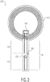
- the first tamper detection device 100 includes an antenna 102, a detection circuit 104, and a detection element 106 (e.g. wire, distributed L, C or R, discrete L, C or R).
- the detection element 106 includes an undisturbed breach element 108 (e.g. pull linkage, shear element, tear strip, etc.), a top portion 110, and a bottom portion 112.
- Figure 2 is an example of the first tamper detection device 100 in a disturbed state. A disturbed breach element 202 is shown. Figures 1 and 2 are now discussed together.
- the detection circuit 104 in one example embodiment is configured to be powered by a near-field-communication (NFC) signal and store a status of a detection element 106.
- the detection circuit 104 is configured to set the status to undisturbed in response to an undisturbed state of the detection element 106.
- the detection circuit 104 is configured to set the status to disturbed in response to a disturbed state of the detection element 106.
- the undisturbed state in some example embodiments is defined as a state opposite to the disturbed state.
- the detection circuit 104 in one example, is included in an NXP Semiconductors NTAG TAG 21x family chip (NFC Type 2 tag compliant).
- the antenna 102 is connected to a set of antenna pads on the detection circuit 104 (e.g. IC, chip, etc.) and the NTAG tamper detection element 106 is connected to a set of tamper pads on the detection circuit 104.
- the detection circuit 104 is configured to electrically report the detection element 106 status in response to a wireless query signal.
- the detection circuit 104 is configured to continue to operate and electrically report the detection element 106 status even after the detection element 106 has been placed in the disturbed state. Continued operation is possible since the antenna 102 remains coupled to the detection circuit 104 and are configured to continue to interoperate even after the detection element 106 is disturbed.
- the detection circuit 104 is configured to set to the disturbed status in response to a change in either an inductance or a capacitance of the detection element 106.
- the inductance or the capacitance can either be distributed over the detection element 106 or a discrete part of the detection element 106.
- the detection circuit 104 is set to the disturbed status in response to a change in a distributed resistance of the detection element 106.
- the tamper detection device 100 can be coupled to a package to detect tampering.
- the package in various example embodiments can be: a bottle, a box, a bag, a pharmaceutical, a single-use device, an electronic device, an entry device, a security device, a stamp, an envelope, an electronic seal.
- the detection circuit 104 is configured to interpret changes in either the inductance or the capacitance of the detection element 106 and set to the disturbed status in response to at least one of: a breach, a tear, a displacement, a repair, or an electrical variation that exceeds a predetermined tolerance, in the detection element 106.
- Some example embodiments of the tamper detection device 100 include a plurality of detection elements 106.
- the detection circuit 104 could then be configured to report a number of detection elements 106 having the disturbed status and perhaps rank the importance of each disturbed detection elements 106.
- Some detection elements 106 may be more important to the integrity of the package's contents. Customized responses to such specific subsets of detection elements 106 disturbed could then be crafted.
- Figure 3A is an example of a second tamper detection device 300 having a distributed detection element 306.
- the second tamper detection device 300 includes an antenna 302, a detection circuit 304, the distributed detection element 306, and a breach element 310.
- the distributed detection element 306 can be at least one of: a detection wire having a distributed inductance, capacitance, or resistance.
- Figure 3B is an example of the second tamper detection device 300 having a discrete detection element 308.
- the discrete detection element 308 can be at least one of: a discrete inductance, capacitance, diode, or resistance coupled to the detection wire.
- the detection element 308 is on one side of the breach element 310 (e.g. pull linkage, shear element, tear strip, etc.), and the detection circuit 304 is on the other side of the breach element 310.
- the resistance or diode in the discrete detection element 308 is a bare chip which is connected with two bond wires.
- FIG. 4 is an example of a third tamper detection device 400 having a first reference oscillator 404.
- the third tamper detection device 400 includes a detection circuit 402, the first reference oscillator 404, a detection oscillator 414, a comparator circuit 424 that generates an in range signal/value, and an in_range read out 430.
- the first reference oscillator 404 includes a resonant circuit 408 and a divider 410, and generates a ref_clock signal 406.
- the detection oscillator 414 includes an energy storage element 416 (e.g. capacitance) and generates a det_clock signal 418.
- the divider 410 is included since the det_clock (e.g. LC_clock) 418 signal frequency is much greater than the ref clock 406 frequency.
- the detection oscillator 414 is coupled to the detection element 420 (e.g. distributed inductance) having a breach element 422.
- An alternate paradigm is to count and compare the ref clock signal 406 and the det_clock signal 418 and set the detection element 420 status to the disturbed status if the clock counts differ by more than a predetermined tolerance.
- the detection oscillator's 414 frequency is set based on the inductive and capacitive energy storage properties of the energy storage element 416 and the detection element 420.
- detection circuit's 402 comparison route can be implemented in a variety of ways, an example implementation is now discussed.
- the comparator circuit 424 When the third tamper detection device 400 is powered by an active NFC field, the comparator circuit 424 is triggered to start 434 counting a number of LC clocks cycles within a time window 432 (i.e. determine the detection oscillator's 414 frequency). In some example embodiments, however, the reference clock (ref_clock) signal 406 first is synchronized with the detection clock (det_clock/LC_clock) 418 and before counting is started 434.
- the comparator circuit 424 then counts 436, during the defined time window 432, a number of det_clock pulses in a N ⁇ ref_clock period, where N is an integer.
- the LC circuit 416/422 causes the detection element's 420 LC tank circuit to oscillate at a first frequency when undisturbed and a second frequency when disturbed.
- the in_range read out 430 is read by another device (e.g. a smartphone via a wireless connection) during a defined timeslot.
- the third tamper detection device 400 in some example embodiments, is only operational during a minimum function timeslot.
- the detection circuit 402 is configured so that, once the status is set to disturbed, the status cannot afterwards be reset to undisturbed.
- manipulations of the detection element 420 such as opening, reclosing, and/or replacing are detectable.
- the detection element 420 is a wire in the range of 3.5 cm long and 0.5 cm wide, and has an inductance (L) and a capacitor (C) having a value small enough to be embedded in a CMOS device.
- Figure 5 is an example of the third tamper detection 400 device having a second reference oscillator 502.
- the operation of this example embodiment is substantially similar to that discussed in Figure 4 , except in this example the first reference oscillator 404 is replaced by a second reference oscillator 502 having an NFC signal derived reference frequency circuit 504 and a divider 506.
- the NFC signal derived reference frequency circuit 504 is based on the 13.56 MHz. of the NFC transmission field.
- the ref_clock 406 is a divided value of ref frequency of the transmission field 504.
- Figure 6 is an example of a fourth tamper detection device 600.
- the fourth tamper detection device 600 detection circuit 602 is based on the third tamper detection device 400 detection circuit 402, but with modifications as shown in Figure 6 .
- the modifications include a detection oscillator 604 has an energy storage element 606 (i.e. inductance) and generating a det clock signal 608. Also a detection element 610 (e.g. distributed capacitance) includes a first conductor 612, an isolator 614, a second conductor 616, and an undisturbed breach element 618. In this example the detection element 610 is a capacitance distributed between the two conductors 612, 616 on either side of the isolator 614, and can have any shape or size. One example of a cross-section of the detection element 610 is also shown.
- an energy storage element 606 i.e. inductance
- a detection element 610 e.g. distributed capacitance
- the detection element 610 is a capacitance distributed between the two conductors 612, 616 on either side of the isolator 614, and can have any shape or size.
- a cross-section of the detection element 610 is also shown.
- the detection element 610 in one embodiment could be wrapped around a package, such as a bottle and bottle cap.
- FIG. 7 is an example of a fifth tamper detection device 700.
- the fifth tamper detection device 700 includes a detection circuit 702, a detection oscillator 704 (i.e. a ring oscillator) that generates a det_clock signal 708, and a detection element 710 (e.g. delay element in the form of a distributed capacitance).
- a detection oscillator 704 i.e. a ring oscillator
- a detection element 710 e.g. delay element in the form of a distributed capacitance
- the detection element 710 includes a first conductor 712, an isolator 714, a second conductor 716, and an undisturbed breach element 718.
- the detection oscillator 704 is a ring oscillator circuit, and the detection circuit 702 is configured to set the frequency of the detection oscillator 704 based on a delay characteristic of the detection element 710.
- FIG 8 is an example of a sixth tamper detection device 800.
- the sixth tamper detection device 800 includes an antenna 802, a detection circuit 804 and a detection element 806.
- the detection element 806 is a distributed capacitance, in the form of a first conductor 812, an isolator 814, a second conductor 816.
- the detection element 806 also includes an undisturbed breach element 818.
- the tamper detection device 800 could additionally have a sticky surface to adhere to another package requiring tamper detection.
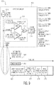
- Figure 9 is an example of a seventh tamper detection device 900 having a distributed resistance detection element 904.
- the seventh tamper detection device 900 includes a detection circuit 902 and the distributed resistance detection element 904.
- the detection circuit 902 includes a comparator circuit 906, a current source 914 and a storage element 916.
- the comparator circuit 906 includes a first comparator 908 (e.g. comp_h), a second comparator 910 (e.g. comp_1), and an AND gate 912.
- the comparator circuit 906 also includes additional logic, etc. for executing the following sampling and storage routine.
- the continuous measurement and storage routine includes, sample and compare 920 during the time window 918, a voltage drop (i.e. Vbreach) over the detection element 904 during a predefined time window 918.
- a voltage drop i.e. Vbreach
- the value of in_range is stored in the storage element 916, and can be read out 926 in response to a query signal.
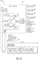
- Figure 10 is an example 1000 of the seventh tamper detection device 900 having a discrete resistance detection element 1002.
- the operation of this example embodiment is substantially similar to that discussed in Figure 9 , except in this example the detection element is the discrete resistance detection element 1002.
- Figure 11 is an example 1100 of the seventh tamper detection device having a discrete diode detection element 1102.
- the operation of this example embodiment is also substantially similar to that discussed in Figure 9 , except in this example the detection element is the discrete diode detection element 1102.
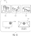
- Figure 12 is an example set of tamper detection device applications 1200. Shown are how tamper detection devices could be applied to bottles 1202, boxes 1204, pharmaceuticals 1206, stamps 1208 and envelopes 1210. Additionally tamper detection devices could be added to gas meters, water meters, electrical meters, as a seal of trucks, on suitcases, and so on.
- one or more tamper detection devices in various examples can be used to protect: closures for spirits and wines, packaging for high value goods (e.g. beauty care products), packaging for highly counterfeited products, and/or packaging for Pharmaceuticals.
- a tamper detection device comprising: a detection circuit, configured to be powered by a near-field-communication (NFC) signal and store a status of a detection element; wherein the detection circuit is configured to set the status to undisturbed in response to an undisturbed state of the detection element; wherein the detection circuit is configured to set the status to disturbed in response to a disturbed state of the detection element; and wherein the detection circuit is configured to electrically report the detection element status in response to a wireless query signal.
- NFC near-field-communication
Landscapes
- Engineering & Computer Science (AREA)
- Physics & Mathematics (AREA)
- Microelectronics & Electronic Packaging (AREA)
- Computer Hardware Design (AREA)
- General Physics & Mathematics (AREA)
- Theoretical Computer Science (AREA)
- Electromagnetism (AREA)
- Chemical & Material Sciences (AREA)
- Computer Networks & Wireless Communication (AREA)
- Health & Medical Sciences (AREA)
- Electrochemistry (AREA)
- Life Sciences & Earth Sciences (AREA)
- Analytical Chemistry (AREA)
- Biochemistry (AREA)
- General Health & Medical Sciences (AREA)
- Immunology (AREA)
- Pathology (AREA)
- Chemical Kinetics & Catalysis (AREA)
- Burglar Alarm Systems (AREA)
- Alarm Systems (AREA)
Claims (14)
- Manipulationsdetektionseinrichtung (100, 300, 400, 600, 700, 800, 900), umfassend:eine Detektionsschaltung (104, 304, 402, 602, 702, 802, 902), die konfiguriert ist, um durch ein NFC-Signal (NFC = Near Field Communication) betrieben zu werden und einen Status eines Detektionselements (106, 306, 308, 420, 610, 710, 806, 904) zu speichern;wobei die Detektionsschaltung konfiguriert ist, um den Status als Reaktion auf einen Ungestört-Zustand des Detektionselements auf ungestört zu setzen;wobei die Detektionsschaltung konfiguriert ist, um den Status als Reaktion auf einen Gestört-Zustand des Detektionselements auf gestört zu setzen;wobei die Detektionsschaltung konfiguriert ist, um den Detektionselementstatus als Reaktion auf ein Drahtlosabfragesignal elektrisch zu melden; undwobei die Detektionsschaltung so konfiguriert ist, dass, sobald der Status auf gestört gesetzt ist, der Status anschließend nicht auf ungestört zurückgesetzt werden kann.
- Einrichtung (100, 300, 400, 600, 700, 800, 900) nach Anspruch 1:
wobei die Detektionsschaltung (104, 304, 402, 602, 702, 802, 902) konfiguriert ist, um weiter betrieben zu werden und den Status des Detektionselements (106, 306, 308, 420, 610, 710, 806, 904) elektrisch zu melden, selbst wenn das Detektionselement bereits im Gestört-Zustand ist. - Einrichtung (100, 300, 400, 600, 700, 800, 900) nach einem vorhergehenden Anspruch:ferner umfassend eine Antenne (102, 302, 802), die an die Detektionsschaltung (104, 304, 402, 602, 702, 802, 902) gekoppelt ist; undwobei die Antenne und die Detektionsschaltung konfiguriert sind, um weiter zusammenzuarbeiten, selbst wenn das Detektionselement (106, 306, 308, 420, 610, 710, 806, 904) bereits gestört ist.
- Einrichtung (100, 300, 400, 600, 700, 800, 900) nach einem vorhergehenden Anspruch:wobei die Detektionsschaltung (104, 304, 402, 602, 702, 802, 902) einen Referenzoszillator (404, 502) und einen Detektionsoszillator (414, 604, 704) enthält;wobei die Detektionsschaltung konfiguriert ist, um eine Anzahl von Detektionsoszillatortaktzyklen zu zählen und mit einer Anzahl von Referenzoszillatortaktzyklen zu vergleichen; undwobei die Detektionsschaltung den Status des Detektionselements (106, 306, 308, 420, 610, 710, 806, 904) auf den Gestört-Status setzt, wenn die Zählung der Anzahl von Detektionsoszillatortaktzyklen über oder unter einem vorher bestimmten Toleranzbereich liegt.
- Einrichtung (100, 300, 400, 600, 700, 800, 900) nach einem vorhergehenden Anspruch:wobei die Detektionsschaltung (104, 304, 402, 602, 702, 802, 902) einen Referenzoszillator (404, 502) und einen Detektionsoszillator (414, 604, 704) enthält; undwobei die Detektionsschaltung konfiguriert ist, um die Frequenz des Referenzoszillators und die Frequenz des Detektionsoszillators zu vergleichen und den Status des Detektionselements (106, 306, 308, 420, 610, 710, 806, 904) auf den Gestört-Status zu setzen, wenn die Frequenzen um mehr als einen vorher bestimmten Toleranzbereich voneinander abweichen.
- Einrichtung (100, 300, 400, 600, 700, 800, 900) nach Anspruch 5:
wobei eine Frequenz des Referenzoszillators (404, 502) geringer als die Frequenz des Detektionsoszillators (414, 604, 704) ist. - Einrichtung (100, 300, 400, 600, 700, 800, 900) nach Anspruch 5 oder 6:wobei der Detektionsoszillator (414, 604, 704) an das Detektionselement (106, 306, 308, 420, 610, 710, 806, 904) gekoppelt ist; undwobei die Detektionsschaltung (104, 304, 402, 602, 702, 802, 902) konfiguriert ist, um die Frequenz des Detektionsoszillators basierend auf einer Energiespeichereigenschaft des Detektionselements zu setzen.
- Einrichtung (100, 300, 400, 600, 700, 800, 900) nach einem der Ansprüche 5 bis 7:
wobei die Detektionsschaltung (104, 304, 402, 602, 702, 802, 902) konfiguriert ist, um die Frequenz des Detektionsoszillators (414, 604, 704) basierend auf entweder einer Induktivität oder einer Kapazität des Detektionselements (106, 306, 308, 420, 610, 710, 806, 904) zu setzen. - Einrichtung (100, 300, 400, 600, 700, 800, 900) nach einem der Ansprüche 5 bis 8:wobei der Detektionsoszillator (414, 604, 704) eine Ringoszillatorschaltung enthält; undwobei die Detektionsschaltung (104, 304, 402, 602, 702, 802, 902) konfiguriert ist, um die Frequenz des Detektionsoszillators basierend auf einem Verzögerungsmerkmal des Detektionselements (106, 306, 308, 420, 610, 710, 806, 904) zu setzen.
- Einrichtung (100, 300, 400, 600, 700, 800, 900) nach einem vorhergehenden Anspruch:
wobei die Detektionsschaltung (104, 304, 402, 602, 702, 802, 902) konfiguriert ist, um als Reaktion auf eine Änderung einer Induktivität und/oder einer Kapazität und/oder eines verteilten Widerstands des Detektionselements (106, 306, 308, 420, 610, 710, 806, 904) auf den Gestört-Status gesetzt zu werden. - Einrichtung (100, 300, 400, 600, 700, 800, 900) nach einem vorhergehenden Anspruch:
wobei das Detektionselement (106, 306, 308, 420, 610, 710, 806, 904) eine diskrete Induktivität und/oder eine diskrete Kapazität und/oder eine diskrete Diode und/oder einen diskreten Widerstand enthält. - Einrichtung (100, 300, 400, 600, 700, 800, 900) nach einem vorhergehenden Anspruch:wobei die Manipulationsdetektionseinrichtung an ein Produkt gekoppelt ist; undwobei das Produkt mindestens eines von Folgendem ist: eine Flasche (1202), ein Kasten (1204), eine Tasche, ein Pharmazeutikum (1206), ein Einmalprodukt, eine elektronische Einrichtung, eine Zugangseinrichtung, eine Sicherheitseinrichtung, eine Briefmarke (1208), ein Briefumschlag (1210), eine elektronische Plombe, ein Gaszähler, ein Wasserzähler, ein Stromzähler, eine Plombe von LKWs oder ein Koffer.
- Einrichtung (100, 300, 400, 600, 700, 800, 900) nach einem vorhergehenden Anspruch:
wobei die Detektionsschaltung (104, 304, 402, 602, 702, 802, 902) als Reaktion auf eine Bruchstelle und/oder einen Riss und/oder eine Verlagerung und/oder eine Reparatur und/oder eine elektrische Veränderung, die eine vorher bestimmte Toleranz überschreitet, im Detektionselement (106, 306, 308, 420, 610, 710, 806, 904) auf den Gestört-Status gesetzt wird. - Einrichtung (100, 300, 400, 600, 700, 800, 900) nach einem vorhergehenden Anspruch:wobei die Detektionsschaltung (104, 304, 402, 602, 702, 802, 902) eine Komparatorschaltung (906) enthält;wobei die Komparatorschaltung konfiguriert ist, um einen Spannungsabfall über das Detektionselement (106, 306, 308, 420, 610, 710, 806, 904) während eines definierten Zeitfensters zu erfassen; undwobei die Komparatorschaltung den Detektionselementstatus auf den Gestört-Status setzt, wenn der Spannungsabfall über oder unter einem vorher bestimmten Toleranzbereich liegt, und wobei das Detektionselement einen verteilten Widerstand und/oder einen diskreten Widerstand und/oder eine Diode enthält.
Applications Claiming Priority (1)
| Application Number | Priority Date | Filing Date | Title |
|---|---|---|---|
| US15/366,419 US10725077B2 (en) | 2016-12-01 | 2016-12-01 | Tamper detector |
Publications (2)
| Publication Number | Publication Date |
|---|---|
| EP3330896A1 EP3330896A1 (de) | 2018-06-06 |
| EP3330896B1 true EP3330896B1 (de) | 2021-03-31 |
Family
ID=60569712
Family Applications (1)
| Application Number | Title | Priority Date | Filing Date |
|---|---|---|---|
| EP17204847.2A Active EP3330896B1 (de) | 2016-12-01 | 2017-12-01 | Manipulationsdetektor |
Country Status (2)
| Country | Link |
|---|---|
| US (1) | US10725077B2 (de) |
| EP (1) | EP3330896B1 (de) |
Families Citing this family (10)
| Publication number | Priority date | Publication date | Assignee | Title |
|---|---|---|---|---|
| WO2019238791A1 (en) * | 2018-06-12 | 2019-12-19 | Anheuser-Busch Inbev S.A. | Smart packaging |
| WO2021099353A1 (en) * | 2019-11-21 | 2021-05-27 | Merck Patent Gmbh | Rfid label |
| DE102020000303A1 (de) * | 2020-01-17 | 2021-07-22 | Giesecke+Devrient Currency Technology Gmbh | Schaltungsanordnung eines elektronischen Siegels |
| US20220318589A1 (en) * | 2021-03-31 | 2022-10-06 | Paul Abner | Methods and systems of a tamper-evident seal |
| US12124905B1 (en) * | 2021-12-17 | 2024-10-22 | Wells Fargo Bank, N.A. | Transaction instrument with features for destruction and disposal |
| US12292461B2 (en) * | 2022-02-28 | 2025-05-06 | Texas Instruments Incorporated | Resonant frequency change detection |
| US12293008B2 (en) | 2022-05-13 | 2025-05-06 | Nxp Usa, Inc. | Security device |
| EP4589471A4 (de) * | 2022-09-12 | 2025-12-31 | Toppan Holdings Inc | Manipulationsdetektionsetikett und behälter mit etikett |
| US12351126B1 (en) * | 2022-10-13 | 2025-07-08 | David Rosales | Alarm system and method for detecting a removal of a catalytic converter or other item |
| US12557604B2 (en) | 2024-03-15 | 2026-02-17 | Nxp B.V. | Degradation circuit |
Family Cites Families (67)
| Publication number | Priority date | Publication date | Assignee | Title |
|---|---|---|---|---|
| US4262284A (en) | 1978-06-26 | 1981-04-14 | Stieff Lorin R | Self-monitoring seal |
| US4711368A (en) | 1986-04-11 | 1987-12-08 | Leon Simons | Tamper proof package with electrical circuit |
| US5117457A (en) | 1986-11-05 | 1992-05-26 | International Business Machines Corp. | Tamper resistant packaging for information protection in electronic circuitry |
| US4890763A (en) | 1987-01-27 | 1990-01-02 | Tsl, Incorporated | Tamper resistant package and method of making same |
| US4764952A (en) | 1987-03-18 | 1988-08-16 | Feliu Horace G | Telecommunications device for reading power meters |
| US5117222A (en) | 1990-12-27 | 1992-05-26 | Guardian Technologies, Inc. | Tamper indicating transmitter |
| CA2125786C (fr) | 1991-12-19 | 2007-07-31 | Ake Gustafson | Dispositif de scellement de securite |
| GB9203931D0 (en) | 1992-02-25 | 1992-04-08 | Nmc Flexible Packaging Limited | Tamper indicating packages |
| US5389738A (en) | 1992-05-04 | 1995-02-14 | Motorola, Inc. | Tamperproof arrangement for an integrated circuit device |
| US5323150A (en) | 1992-06-11 | 1994-06-21 | Micron Technology, Inc. | Method for reducing conductive and convective heat loss from the battery in an RFID tag or other battery-powered devices |
| US5298884A (en) | 1992-10-16 | 1994-03-29 | Bi Incorporated | Tamper detection circuit and method for use with wearable transmitter tag |
| US5457748A (en) | 1992-11-30 | 1995-10-10 | Motorola, Inc. | Method and apparatus for improved security within encrypted communication devices |
| US5464092A (en) | 1994-06-06 | 1995-11-07 | Seeley; Dennis H. | Container having an audible signaling device |
| US5523740A (en) | 1995-04-24 | 1996-06-04 | Detection Systems, Inc. | Wearable transmitter assembly |
| US5650766A (en) | 1995-04-24 | 1997-07-22 | Detection Systems, Inc. | Wearable transmitter with optical tamper detection |
| US5949059A (en) | 1996-12-09 | 1999-09-07 | International Business Machines Corporation | Tamper evident labelling system with embedded storage device |
| US5880523A (en) | 1997-02-24 | 1999-03-09 | General Instrument Corporation | Anti-tamper integrated circuit |
| WO2000016284A1 (en) | 1998-09-11 | 2000-03-23 | Key-Trak, Inc. | Tamper detection and prevention for an object control and tracking system |
| US6501390B1 (en) | 1999-01-11 | 2002-12-31 | International Business Machines Corporation | Method and apparatus for securely determining aspects of the history of a good |
| ES2351549T3 (es) | 2000-03-21 | 2011-02-07 | Mikoh Corporation | Una etiqueta de identificación por radiofrecuencia con indicación de manipulación indebida. |
| CA2340533A1 (en) | 2001-03-13 | 2002-09-13 | Claude Houde | Fiber optic based security system |
| US7299981B2 (en) | 2001-05-21 | 2007-11-27 | Scott Laboratories, Inc. | Smart supplies, components and capital equipment |
| US20030011474A1 (en) | 2001-07-13 | 2003-01-16 | Ng Sing King | Circuit and method for electronic security seal |
| US7287169B2 (en) | 2002-10-10 | 2007-10-23 | Stmicroelectronics, Inc. | Electronic device and timer therefor with tamper event stamp features and related methods |
| US20050017845A1 (en) | 2003-07-22 | 2005-01-27 | Shellans Mark Honore | Tagging and tracking system |
| US7017807B2 (en) * | 2003-09-08 | 2006-03-28 | Francis M. Claessens | Apparatus and method for detecting tampering with containers and preventing counterfeiting thereof |
| US7034689B2 (en) | 2004-01-28 | 2006-04-25 | Bertrand Teplitxky | Secure product packaging system |
| US7239238B2 (en) | 2004-03-30 | 2007-07-03 | E. J. Brooks Company | Electronic security seal |
| US8336085B2 (en) | 2004-11-15 | 2012-12-18 | Microsoft Corporation | Tuning product policy using observed evidence of customer behavior |
| US20060145848A1 (en) | 2004-12-28 | 2006-07-06 | Alpha Security Products, Inc. | Electronic security device and system for articles of merchandise |
| US7772974B2 (en) * | 2005-02-28 | 2010-08-10 | Cypak Ab | Tamper evident seal system and method |
| US7385491B2 (en) * | 2005-09-28 | 2008-06-10 | Itt Manufacturing Enterprises, Inc. | Tamper monitor circuit |
| US7368935B2 (en) | 2005-10-18 | 2008-05-06 | Honeywell International Inc. | Tamper response system for integrated circuits |
| US7652577B1 (en) | 2006-02-04 | 2010-01-26 | Checkpoint Systems, Inc. | Systems and methods of beamforming in radio frequency identification applications |
| US7410103B2 (en) | 2006-03-13 | 2008-08-12 | Andreas Rolf Nagel | System, method and device to detect product tampering |
| US8050657B2 (en) * | 2006-03-28 | 2011-11-01 | Texas Instruments Incorporated | Tamper resistant circuitry and portable electronic devices |
| US7887755B2 (en) | 2006-09-20 | 2011-02-15 | Binforma Group Limited Liability Company | Packaging closures integrated with disposable RFID devices |
| US7710269B2 (en) | 2007-01-11 | 2010-05-04 | University Of Southern California | Systems and methods to prevent counterfeit, grey and black market proliferation of pharmaceutical, medical and other products |
| JP4281821B2 (ja) | 2007-05-01 | 2009-06-17 | ソニー株式会社 | 上映システム |
| US7961100B2 (en) | 2007-08-03 | 2011-06-14 | Checkpoint Systems, Inc. | Theft deterrent device |
| US7937596B2 (en) * | 2007-08-30 | 2011-05-03 | Harris Corporation | Adaptable microcontroller based security monitor |
| US8042739B2 (en) | 2007-09-28 | 2011-10-25 | The United States Of America As Represented By The Administrator Of The National Aeronautics And Space Administration | Wireless tamper detection sensor and sensing system |
| US8383163B2 (en) | 2008-01-29 | 2013-02-26 | Ultradent Products, Inc. | Fluoride varnish compositions including an organo phosphoric acid adhesion promoting agent |
| US20100289629A1 (en) | 2008-10-28 | 2010-11-18 | Cooper Technologies Company | Load Control Device with Two-Way Communication Capabilities |
| US8598890B2 (en) * | 2009-02-23 | 2013-12-03 | Lewis Innovative Technologies | Method and system for protecting products and technology from integrated circuits which have been subject to tampering, stressing and replacement as well as detecting integrated circuits that have been subject to tampering |
| US8186731B1 (en) | 2009-04-14 | 2012-05-29 | Sandia Corporation | Tamper indicating seal |
| US9082057B2 (en) | 2009-08-19 | 2015-07-14 | Intelleflex Corporation | RF device with tamper detection |
| JP5099651B2 (ja) | 2010-03-30 | 2012-12-19 | Necインフロンティア株式会社 | 携帯端末 |
| US8499173B2 (en) | 2010-11-23 | 2013-07-30 | Lockheed Martin Corporation | Apparatus and method for protection of circuit boards from tampering |
| US10153901B2 (en) | 2010-11-23 | 2018-12-11 | Concierge Holdings, Inc. | System and method for verifying user identity in a virtual environment |
| US8884764B2 (en) * | 2011-02-25 | 2014-11-11 | Avery Dennison Corporation | Method, system, and apparatus for RFID removal detection |
| WO2012122994A1 (en) * | 2011-03-11 | 2012-09-20 | Kreft Heinz | Off-line transfer of electronic tokens between peer-devices |
| US9058554B2 (en) | 2011-11-25 | 2015-06-16 | Smartrac Ip B.V. | Transponder with tamper protection |
| US20130135104A1 (en) | 2011-11-29 | 2013-05-30 | Upm Rfid Oy | Radio-frequency transponder comprising a tamper loop functionality |
| US9024616B2 (en) | 2011-12-19 | 2015-05-05 | Tyco Safety Products Canada Ltd. | Signaling circuit and method to detect zone status |
| US20140091781A1 (en) | 2012-09-28 | 2014-04-03 | Hutchison International Ports Enterprises Limited | Security system |
| US9031503B2 (en) * | 2013-02-20 | 2015-05-12 | Nxp B.V. | Wireless data communications |
| US9658254B2 (en) | 2013-06-28 | 2017-05-23 | Landis+Gyr, Inc. | Magnetic tampering detection in a utility meter |
| US9342710B2 (en) | 2013-11-21 | 2016-05-17 | Nxp B.V. | Electronic tamper detection |
| US9741231B2 (en) | 2014-03-10 | 2017-08-22 | Nxp B.V. | Tamper/damage detection |
| US9578763B1 (en) | 2014-05-22 | 2017-02-21 | Square, Inc. | Tamper detection using internal power signal |
| US11695448B2 (en) | 2014-07-31 | 2023-07-04 | Gilbarco Inc. | Fuel dispenser anti-skimming input device |
| US9519904B2 (en) | 2014-10-19 | 2016-12-13 | Thin Film Electronics Asa | NFC/RF mechanism with multiple valid states for detecting an open container, and methods of making and using the same |
| US10502771B2 (en) | 2016-01-29 | 2019-12-10 | Landis+Gyr Llc | Detecting current measurement tampering by current transformer parallel impedance |
| EP3319014B1 (de) | 2016-11-04 | 2021-01-20 | EM Microelectronic-Marin SA | Verfahren zur bereitstellung eines lesers mit einem betrugssicheren schleifenstatus eines funkfrequenztransponders |
| US9859226B1 (en) | 2016-12-13 | 2018-01-02 | International Business Machines Corporation | Core-shell particles for anti-tampering applications |
| EP3340114B1 (de) | 2016-12-22 | 2020-09-30 | EM Microelectronic-Marin SA | Rfid-schaltkreis mit zwei kommunikationsfrequenzen, der mit einem sicherungskreislauf ausgestattet ist |
-
2016
- 2016-12-01 US US15/366,419 patent/US10725077B2/en active Active
-
2017
- 2017-12-01 EP EP17204847.2A patent/EP3330896B1/de active Active
Non-Patent Citations (1)
| Title |
|---|
| None * |
Also Published As
| Publication number | Publication date |
|---|---|
| US20180156854A1 (en) | 2018-06-07 |
| EP3330896A1 (de) | 2018-06-06 |
| US10725077B2 (en) | 2020-07-28 |
Similar Documents
| Publication | Publication Date | Title |
|---|---|---|
| EP3330896B1 (de) | Manipulationsdetektor | |
| US10579919B2 (en) | NFC/RF mechanism with multiple valid states for detecting an open container, and methods of making and using the same | |
| CN107437106B (zh) | 篡改检测装置 | |
| US7017807B2 (en) | Apparatus and method for detecting tampering with containers and preventing counterfeiting thereof | |
| US10371737B2 (en) | Wireless mechanism for detecting an open or closed container, and methods of making and using the same | |
| US9893889B2 (en) | Anti-counterfeiting label preserving functionality after use | |
| US7839288B2 (en) | Sealing detection mechanism using RFID tag for container | |
| EP2497054B1 (de) | System für ein versorgungskettenmanagement | |
| US20070008121A1 (en) | RFID disablement detection of tampering | |
| EP2794304B1 (de) | Messfühler | |
| CN114127760A (zh) | 产品跟踪 | |
| US20100079921A1 (en) | Semiconductor Device | |
| CN106557805A (zh) | 安全无线射频识别卷标、系统及其方法 | |
| US20260015140A1 (en) | Secure shipment container and related methods | |
| Wang et al. | All-around package security using radio frequency identification threads | |
| US20080198011A1 (en) | Radio-frequency identification tags for preventing and detecting tampering | |
| EP4508565A1 (de) | Elektronisches etikett | |
| GB2535971A (en) | Universal RFID bottle tag | |
| TW201031153A (en) | Modulation circuit and semiconductor device including the same | |
| US20230415961A1 (en) | Event activated controls and display for a shipping container | |
| KR102215010B1 (ko) | 포장물의 개봉 검출기를 갖는 무선 통신 장치 | |
| US20240179857A1 (en) | Smart sealing using sensors and conductive inks | |
| CN204102171U (zh) | 基于射频技术的无线温度电子标签 | |
| WO2023069364A1 (en) | Secure shipment container and related methods |
Legal Events
| Date | Code | Title | Description |
|---|---|---|---|
| PUAI | Public reference made under article 153(3) epc to a published international application that has entered the european phase |
Free format text: ORIGINAL CODE: 0009012 |
|
| STAA | Information on the status of an ep patent application or granted ep patent |
Free format text: STATUS: THE APPLICATION HAS BEEN PUBLISHED |
|
| AK | Designated contracting states |
Kind code of ref document: A1 Designated state(s): AL AT BE BG CH CY CZ DE DK EE ES FI FR GB GR HR HU IE IS IT LI LT LU LV MC MK MT NL NO PL PT RO RS SE SI SK SM TR |
|
| AX | Request for extension of the european patent |
Extension state: BA ME |
|
| STAA | Information on the status of an ep patent application or granted ep patent |
Free format text: STATUS: REQUEST FOR EXAMINATION WAS MADE |
|
| 17P | Request for examination filed |
Effective date: 20181206 |
|
| RBV | Designated contracting states (corrected) |
Designated state(s): AL AT BE BG CH CY CZ DE DK EE ES FI FR GB GR HR HU IE IS IT LI LT LU LV MC MK MT NL NO PL PT RO RS SE SI SK SM TR |
|
| STAA | Information on the status of an ep patent application or granted ep patent |
Free format text: STATUS: EXAMINATION IS IN PROGRESS |
|
| 17Q | First examination report despatched |
Effective date: 20200120 |
|
| GRAP | Despatch of communication of intention to grant a patent |
Free format text: ORIGINAL CODE: EPIDOSNIGR1 |
|
| STAA | Information on the status of an ep patent application or granted ep patent |
Free format text: STATUS: GRANT OF PATENT IS INTENDED |
|
| INTG | Intention to grant announced |
Effective date: 20201012 |
|
| GRAJ | Information related to disapproval of communication of intention to grant by the applicant or resumption of examination proceedings by the epo deleted |
Free format text: ORIGINAL CODE: EPIDOSDIGR1 |
|
| STAA | Information on the status of an ep patent application or granted ep patent |
Free format text: STATUS: EXAMINATION IS IN PROGRESS |
|
| GRAP | Despatch of communication of intention to grant a patent |
Free format text: ORIGINAL CODE: EPIDOSNIGR1 |
|
| STAA | Information on the status of an ep patent application or granted ep patent |
Free format text: STATUS: GRANT OF PATENT IS INTENDED |
|
| GRAS | Grant fee paid |
Free format text: ORIGINAL CODE: EPIDOSNIGR3 |
|
| GRAA | (expected) grant |
Free format text: ORIGINAL CODE: 0009210 |
|
| STAA | Information on the status of an ep patent application or granted ep patent |
Free format text: STATUS: THE PATENT HAS BEEN GRANTED |
|
| INTC | Intention to grant announced (deleted) | ||
| INTG | Intention to grant announced |
Effective date: 20210217 |
|
| RIN1 | Information on inventor provided before grant (corrected) |
Inventor name: VAN LAMMEREN, JOOP PETRUS MARIA Inventor name: VERHOEVEN, HENRI Inventor name: MOONEN, OSWALD |
|
| AK | Designated contracting states |
Kind code of ref document: B1 Designated state(s): AL AT BE BG CH CY CZ DE DK EE ES FI FR GB GR HR HU IE IS IT LI LT LU LV MC MK MT NL NO PL PT RO RS SE SI SK SM TR |
|
| REG | Reference to a national code |
Ref country code: GB Ref legal event code: FG4D Ref country code: CH Ref legal event code: EP |
|
| REG | Reference to a national code |
Ref country code: AT Ref legal event code: REF Ref document number: 1377776 Country of ref document: AT Kind code of ref document: T Effective date: 20210415 |
|
| REG | Reference to a national code |
Ref country code: DE Ref legal event code: R096 Ref document number: 602017035589 Country of ref document: DE |
|
| REG | Reference to a national code |
Ref country code: IE Ref legal event code: FG4D |
|
| REG | Reference to a national code |
Ref country code: LT Ref legal event code: MG9D |
|
| PG25 | Lapsed in a contracting state [announced via postgrant information from national office to epo] |
Ref country code: BG Free format text: LAPSE BECAUSE OF FAILURE TO SUBMIT A TRANSLATION OF THE DESCRIPTION OR TO PAY THE FEE WITHIN THE PRESCRIBED TIME-LIMIT Effective date: 20210630 Ref country code: NO Free format text: LAPSE BECAUSE OF FAILURE TO SUBMIT A TRANSLATION OF THE DESCRIPTION OR TO PAY THE FEE WITHIN THE PRESCRIBED TIME-LIMIT Effective date: 20210630 Ref country code: HR Free format text: LAPSE BECAUSE OF FAILURE TO SUBMIT A TRANSLATION OF THE DESCRIPTION OR TO PAY THE FEE WITHIN THE PRESCRIBED TIME-LIMIT Effective date: 20210331 Ref country code: FI Free format text: LAPSE BECAUSE OF FAILURE TO SUBMIT A TRANSLATION OF THE DESCRIPTION OR TO PAY THE FEE WITHIN THE PRESCRIBED TIME-LIMIT Effective date: 20210331 |
|
| PG25 | Lapsed in a contracting state [announced via postgrant information from national office to epo] |
Ref country code: SE Free format text: LAPSE BECAUSE OF FAILURE TO SUBMIT A TRANSLATION OF THE DESCRIPTION OR TO PAY THE FEE WITHIN THE PRESCRIBED TIME-LIMIT Effective date: 20210331 Ref country code: RS Free format text: LAPSE BECAUSE OF FAILURE TO SUBMIT A TRANSLATION OF THE DESCRIPTION OR TO PAY THE FEE WITHIN THE PRESCRIBED TIME-LIMIT Effective date: 20210331 Ref country code: LV Free format text: LAPSE BECAUSE OF FAILURE TO SUBMIT A TRANSLATION OF THE DESCRIPTION OR TO PAY THE FEE WITHIN THE PRESCRIBED TIME-LIMIT Effective date: 20210331 |
|
| REG | Reference to a national code |
Ref country code: NL Ref legal event code: MP Effective date: 20210331 |
|
| REG | Reference to a national code |
Ref country code: AT Ref legal event code: MK05 Ref document number: 1377776 Country of ref document: AT Kind code of ref document: T Effective date: 20210331 |
|
| PG25 | Lapsed in a contracting state [announced via postgrant information from national office to epo] |
Ref country code: NL Free format text: LAPSE BECAUSE OF FAILURE TO SUBMIT A TRANSLATION OF THE DESCRIPTION OR TO PAY THE FEE WITHIN THE PRESCRIBED TIME-LIMIT Effective date: 20210331 Ref country code: SM Free format text: LAPSE BECAUSE OF FAILURE TO SUBMIT A TRANSLATION OF THE DESCRIPTION OR TO PAY THE FEE WITHIN THE PRESCRIBED TIME-LIMIT Effective date: 20210331 Ref country code: AT Free format text: LAPSE BECAUSE OF FAILURE TO SUBMIT A TRANSLATION OF THE DESCRIPTION OR TO PAY THE FEE WITHIN THE PRESCRIBED TIME-LIMIT Effective date: 20210331 Ref country code: EE Free format text: LAPSE BECAUSE OF FAILURE TO SUBMIT A TRANSLATION OF THE DESCRIPTION OR TO PAY THE FEE WITHIN THE PRESCRIBED TIME-LIMIT Effective date: 20210331 Ref country code: CZ Free format text: LAPSE BECAUSE OF FAILURE TO SUBMIT A TRANSLATION OF THE DESCRIPTION OR TO PAY THE FEE WITHIN THE PRESCRIBED TIME-LIMIT Effective date: 20210331 Ref country code: LT Free format text: LAPSE BECAUSE OF FAILURE TO SUBMIT A TRANSLATION OF THE DESCRIPTION OR TO PAY THE FEE WITHIN THE PRESCRIBED TIME-LIMIT Effective date: 20210331 |
|
| PG25 | Lapsed in a contracting state [announced via postgrant information from national office to epo] |
Ref country code: RO Free format text: LAPSE BECAUSE OF FAILURE TO SUBMIT A TRANSLATION OF THE DESCRIPTION OR TO PAY THE FEE WITHIN THE PRESCRIBED TIME-LIMIT Effective date: 20210331 Ref country code: SK Free format text: LAPSE BECAUSE OF FAILURE TO SUBMIT A TRANSLATION OF THE DESCRIPTION OR TO PAY THE FEE WITHIN THE PRESCRIBED TIME-LIMIT Effective date: 20210331 Ref country code: PT Free format text: LAPSE BECAUSE OF FAILURE TO SUBMIT A TRANSLATION OF THE DESCRIPTION OR TO PAY THE FEE WITHIN THE PRESCRIBED TIME-LIMIT Effective date: 20210802 Ref country code: PL Free format text: LAPSE BECAUSE OF FAILURE TO SUBMIT A TRANSLATION OF THE DESCRIPTION OR TO PAY THE FEE WITHIN THE PRESCRIBED TIME-LIMIT Effective date: 20210331 Ref country code: IS Free format text: LAPSE BECAUSE OF FAILURE TO SUBMIT A TRANSLATION OF THE DESCRIPTION OR TO PAY THE FEE WITHIN THE PRESCRIBED TIME-LIMIT Effective date: 20210731 |
|
| REG | Reference to a national code |
Ref country code: DE Ref legal event code: R097 Ref document number: 602017035589 Country of ref document: DE |
|
| PG25 | Lapsed in a contracting state [announced via postgrant information from national office to epo] |
Ref country code: ES Free format text: LAPSE BECAUSE OF FAILURE TO SUBMIT A TRANSLATION OF THE DESCRIPTION OR TO PAY THE FEE WITHIN THE PRESCRIBED TIME-LIMIT Effective date: 20210331 Ref country code: DK Free format text: LAPSE BECAUSE OF FAILURE TO SUBMIT A TRANSLATION OF THE DESCRIPTION OR TO PAY THE FEE WITHIN THE PRESCRIBED TIME-LIMIT Effective date: 20210331 Ref country code: AL Free format text: LAPSE BECAUSE OF FAILURE TO SUBMIT A TRANSLATION OF THE DESCRIPTION OR TO PAY THE FEE WITHIN THE PRESCRIBED TIME-LIMIT Effective date: 20210331 |
|
| PLBE | No opposition filed within time limit |
Free format text: ORIGINAL CODE: 0009261 |
|
| STAA | Information on the status of an ep patent application or granted ep patent |
Free format text: STATUS: NO OPPOSITION FILED WITHIN TIME LIMIT |
|
| 26N | No opposition filed |
Effective date: 20220104 |
|
| PG25 | Lapsed in a contracting state [announced via postgrant information from national office to epo] |
Ref country code: IS Free format text: LAPSE BECAUSE OF FAILURE TO SUBMIT A TRANSLATION OF THE DESCRIPTION OR TO PAY THE FEE WITHIN THE PRESCRIBED TIME-LIMIT Effective date: 20210731 |
|
| PG25 | Lapsed in a contracting state [announced via postgrant information from national office to epo] |
Ref country code: MC Free format text: LAPSE BECAUSE OF FAILURE TO SUBMIT A TRANSLATION OF THE DESCRIPTION OR TO PAY THE FEE WITHIN THE PRESCRIBED TIME-LIMIT Effective date: 20210331 Ref country code: IT Free format text: LAPSE BECAUSE OF FAILURE TO SUBMIT A TRANSLATION OF THE DESCRIPTION OR TO PAY THE FEE WITHIN THE PRESCRIBED TIME-LIMIT Effective date: 20210331 |
|
| REG | Reference to a national code |
Ref country code: CH Ref legal event code: PL |
|
| GBPC | Gb: european patent ceased through non-payment of renewal fee |
Effective date: 20211201 |
|
| REG | Reference to a national code |
Ref country code: BE Ref legal event code: MM Effective date: 20211231 |
|
| PG25 | Lapsed in a contracting state [announced via postgrant information from national office to epo] |
Ref country code: LU Free format text: LAPSE BECAUSE OF NON-PAYMENT OF DUE FEES Effective date: 20211201 Ref country code: IE Free format text: LAPSE BECAUSE OF NON-PAYMENT OF DUE FEES Effective date: 20211201 Ref country code: GB Free format text: LAPSE BECAUSE OF NON-PAYMENT OF DUE FEES Effective date: 20211201 |
|
| PG25 | Lapsed in a contracting state [announced via postgrant information from national office to epo] |
Ref country code: BE Free format text: LAPSE BECAUSE OF NON-PAYMENT OF DUE FEES Effective date: 20211231 |
|
| PG25 | Lapsed in a contracting state [announced via postgrant information from national office to epo] |
Ref country code: LI Free format text: LAPSE BECAUSE OF NON-PAYMENT OF DUE FEES Effective date: 20211231 Ref country code: CH Free format text: LAPSE BECAUSE OF NON-PAYMENT OF DUE FEES Effective date: 20211231 |
|
| PG25 | Lapsed in a contracting state [announced via postgrant information from national office to epo] |
Ref country code: HU Free format text: LAPSE BECAUSE OF FAILURE TO SUBMIT A TRANSLATION OF THE DESCRIPTION OR TO PAY THE FEE WITHIN THE PRESCRIBED TIME-LIMIT; INVALID AB INITIO Effective date: 20171201 |
|
| PG25 | Lapsed in a contracting state [announced via postgrant information from national office to epo] |
Ref country code: CY Free format text: LAPSE BECAUSE OF FAILURE TO SUBMIT A TRANSLATION OF THE DESCRIPTION OR TO PAY THE FEE WITHIN THE PRESCRIBED TIME-LIMIT Effective date: 20210331 |
|
| PG25 | Lapsed in a contracting state [announced via postgrant information from national office to epo] |
Ref country code: GR Free format text: LAPSE BECAUSE OF FAILURE TO SUBMIT A TRANSLATION OF THE DESCRIPTION OR TO PAY THE FEE WITHIN THE PRESCRIBED TIME-LIMIT Effective date: 20210331 |
|
| P01 | Opt-out of the competence of the unified patent court (upc) registered |
Effective date: 20230725 |
|
| PG25 | Lapsed in a contracting state [announced via postgrant information from national office to epo] |
Ref country code: MK Free format text: LAPSE BECAUSE OF FAILURE TO SUBMIT A TRANSLATION OF THE DESCRIPTION OR TO PAY THE FEE WITHIN THE PRESCRIBED TIME-LIMIT Effective date: 20210331 |
|
| PG25 | Lapsed in a contracting state [announced via postgrant information from national office to epo] |
Ref country code: TR Free format text: LAPSE BECAUSE OF FAILURE TO SUBMIT A TRANSLATION OF THE DESCRIPTION OR TO PAY THE FEE WITHIN THE PRESCRIBED TIME-LIMIT Effective date: 20210331 |
|
| PG25 | Lapsed in a contracting state [announced via postgrant information from national office to epo] |
Ref country code: MT Free format text: LAPSE BECAUSE OF FAILURE TO SUBMIT A TRANSLATION OF THE DESCRIPTION OR TO PAY THE FEE WITHIN THE PRESCRIBED TIME-LIMIT Effective date: 20210331 |
|
| PGFP | Annual fee paid to national office [announced via postgrant information from national office to epo] |
Ref country code: DE Payment date: 20251126 Year of fee payment: 9 |
|
| PGFP | Annual fee paid to national office [announced via postgrant information from national office to epo] |
Ref country code: FR Payment date: 20251120 Year of fee payment: 9 |