EP3332260B1 - Verlustarmer stromsensor und leistungswandler damit - Google Patents
Verlustarmer stromsensor und leistungswandler damit Download PDFInfo
- Publication number
- EP3332260B1 EP3332260B1 EP16833767.3A EP16833767A EP3332260B1 EP 3332260 B1 EP3332260 B1 EP 3332260B1 EP 16833767 A EP16833767 A EP 16833767A EP 3332260 B1 EP3332260 B1 EP 3332260B1
- Authority
- EP
- European Patent Office
- Prior art keywords
- current
- voltage
- output
- switches
- controller
- Prior art date
- Legal status (The legal status is an assumption and is not a legal conclusion. Google has not performed a legal analysis and makes no representation as to the accuracy of the status listed.)
- Active
Links
Images




Classifications
-
- G—PHYSICS
- G01—MEASURING; TESTING
- G01R—MEASURING ELECTRIC VARIABLES; MEASURING MAGNETIC VARIABLES
- G01R19/00—Arrangements for measuring currents or voltages or for indicating presence or sign thereof
- G01R19/04—Measuring peak values or amplitude or envelope of AC or of pulses
-
- G—PHYSICS
- G01—MEASURING; TESTING
- G01R—MEASURING ELECTRIC VARIABLES; MEASURING MAGNETIC VARIABLES
- G01R15/00—Details of measuring arrangements of the types provided for in groups G01R17/00 - G01R29/00, G01R33/00 - G01R33/26 or G01R35/00
- G01R15/14—Adaptations providing voltage or current isolation, e.g. for high-voltage or high-current networks
- G01R15/16—Adaptations providing voltage or current isolation, e.g. for high-voltage or high-current networks using capacitive devices
-
- G—PHYSICS
- G01—MEASURING; TESTING
- G01R—MEASURING ELECTRIC VARIABLES; MEASURING MAGNETIC VARIABLES
- G01R19/00—Arrangements for measuring currents or voltages or for indicating presence or sign thereof
- G01R19/0092—Measuring current only
-
- H—ELECTRICITY
- H02—GENERATION; CONVERSION OR DISTRIBUTION OF ELECTRIC POWER
- H02M—APPARATUS FOR CONVERSION BETWEEN AC AND AC, BETWEEN AC AND DC, OR BETWEEN DC AND DC, AND FOR USE WITH MAINS OR SIMILAR POWER SUPPLY SYSTEMS; CONVERSION OF DC OR AC INPUT POWER INTO SURGE OUTPUT POWER; CONTROL OR REGULATION THEREOF
- H02M1/00—Details of apparatus for conversion
- H02M1/38—Means for preventing simultaneous conduction of switches
-
- H—ELECTRICITY
- H02—GENERATION; CONVERSION OR DISTRIBUTION OF ELECTRIC POWER
- H02M—APPARATUS FOR CONVERSION BETWEEN AC AND AC, BETWEEN AC AND DC, OR BETWEEN DC AND DC, AND FOR USE WITH MAINS OR SIMILAR POWER SUPPLY SYSTEMS; CONVERSION OF DC OR AC INPUT POWER INTO SURGE OUTPUT POWER; CONTROL OR REGULATION THEREOF
- H02M3/00—Conversion of DC power input into DC power output
- H02M3/02—Conversion of DC power input into DC power output without intermediate conversion into AC
- H02M3/04—Conversion of DC power input into DC power output without intermediate conversion into AC by static converters
- H02M3/10—Conversion of DC power input into DC power output without intermediate conversion into AC by static converters using discharge tubes with control electrode or semiconductor devices with control electrode
- H02M3/145—Conversion of DC power input into DC power output without intermediate conversion into AC by static converters using discharge tubes with control electrode or semiconductor devices with control electrode using devices of a triode or transistor type requiring continuous application of a control signal
- H02M3/155—Conversion of DC power input into DC power output without intermediate conversion into AC by static converters using discharge tubes with control electrode or semiconductor devices with control electrode using devices of a triode or transistor type requiring continuous application of a control signal using semiconductor devices only
- H02M3/156—Conversion of DC power input into DC power output without intermediate conversion into AC by static converters using discharge tubes with control electrode or semiconductor devices with control electrode using devices of a triode or transistor type requiring continuous application of a control signal using semiconductor devices only with automatic control of output voltage or current, e.g. switching regulators
- H02M3/158—Conversion of DC power input into DC power output without intermediate conversion into AC by static converters using discharge tubes with control electrode or semiconductor devices with control electrode using devices of a triode or transistor type requiring continuous application of a control signal using semiconductor devices only with automatic control of output voltage or current, e.g. switching regulators including plural semiconductor devices as final control devices for a single load
- H02M3/1588—Conversion of DC power input into DC power output without intermediate conversion into AC by static converters using discharge tubes with control electrode or semiconductor devices with control electrode using devices of a triode or transistor type requiring continuous application of a control signal using semiconductor devices only with automatic control of output voltage or current, e.g. switching regulators including plural semiconductor devices as final control devices for a single load comprising at least one synchronous rectifier element
-
- H—ELECTRICITY
- H02—GENERATION; CONVERSION OR DISTRIBUTION OF ELECTRIC POWER
- H02M—APPARATUS FOR CONVERSION BETWEEN AC AND AC, BETWEEN AC AND DC, OR BETWEEN DC AND DC, AND FOR USE WITH MAINS OR SIMILAR POWER SUPPLY SYSTEMS; CONVERSION OF DC OR AC INPUT POWER INTO SURGE OUTPUT POWER; CONTROL OR REGULATION THEREOF
- H02M7/00—Conversion of AC power input into DC power output; Conversion of DC power input into AC power output
- H02M7/02—Conversion of AC power input into DC power output without possibility of reversal
- H02M7/04—Conversion of AC power input into DC power output without possibility of reversal by static converters
- H02M7/12—Conversion of AC power input into DC power output without possibility of reversal by static converters using discharge tubes with control electrode or semiconductor devices with control electrode
- H02M7/21—Conversion of AC power input into DC power output without possibility of reversal by static converters using discharge tubes with control electrode or semiconductor devices with control electrode using devices of a triode or transistor type requiring continuous application of a control signal
- H02M7/217—Conversion of AC power input into DC power output without possibility of reversal by static converters using discharge tubes with control electrode or semiconductor devices with control electrode using devices of a triode or transistor type requiring continuous application of a control signal using semiconductor devices only
-
- H—ELECTRICITY
- H03—ELECTRONIC CIRCUITRY
- H03K—PULSE TECHNIQUE
- H03K5/00—Manipulating of pulses not covered by one of the other main groups of this subclass
- H03K5/153—Arrangements in which a pulse is delivered at the instant when a predetermined characteristic of an input signal is present or at a fixed time interval after this instant
- H03K5/1532—Peak detectors
-
- G—PHYSICS
- G01—MEASURING; TESTING
- G01R—MEASURING ELECTRIC VARIABLES; MEASURING MAGNETIC VARIABLES
- G01R31/00—Arrangements for testing electric properties; Arrangements for locating electric faults; Arrangements for electrical testing characterised by what is being tested not provided for elsewhere
- G01R31/40—Testing power supplies
- G01R31/42—AC power supplies
-
- H—ELECTRICITY
- H02—GENERATION; CONVERSION OR DISTRIBUTION OF ELECTRIC POWER
- H02M—APPARATUS FOR CONVERSION BETWEEN AC AND AC, BETWEEN AC AND DC, OR BETWEEN DC AND DC, AND FOR USE WITH MAINS OR SIMILAR POWER SUPPLY SYSTEMS; CONVERSION OF DC OR AC INPUT POWER INTO SURGE OUTPUT POWER; CONTROL OR REGULATION THEREOF
- H02M1/00—Details of apparatus for conversion
- H02M1/0003—Details of control, feedback or regulation circuits
- H02M1/0009—Devices or circuits for detecting current in a converter
Definitions
- the present invention relates to current sensors for electrical circuits containing a capacitor, and in particular current sensors for use with power converters.
- US 2014/253073 A1 discloses a bi-directional voltage positioning circuit including a voltage to current converter, a current mirror circuit and a switch.
- the voltage to current converter converts a sensing voltage to a first current.
- the sensing voltage is sensed based on a current flowing through an output coil connected between a switching node and an output node.
- the current mirror circuit mirrors the first current to generate a second current being N times greater than the first current and a third current being M times greater than the first current, N and M being real numbers greater than zero.
- the switch provides a feedback node with one of the second current and third current in response to a switching control signal, and an output voltage of the output node is divided at the feedback node.
- EP 1 014 549 A2 discloses a DC-to-DC power converter comprising at least one power switch, a pulse width modulation circuit for generating pulses for the at least one power switch, an output inductor connected to the at least one power switch and a current sensor that is connected in parallel with the inductor for sensing current passing through the inductor and includes a resistor and a capacitor connected together in series.
- the current sensor is connected to a peak current control loop circuit cooperating with the pulse width modulation circuit for controlling the at least one power switch responsive to the current sensor.
- WO 2006/011098 A1 refers to a switched mode power supply comprising a half bridge circuit or a full bridge circuit.
- a resonant circuit is connected to the bridge circuit and comprises an inductive element and a capacitive element connected in series, the resonant circuit having a resonant frequency.
- the rate of change of a voltage across the resonant circuit is measured.
- a switching frequency of the switching elements is controlled for lowering the rate of change of the voltage across the resonant circuit to a predetermined minimum value.
- US 4 373 141 A discloses a peak detector circuit, wherein an input signal is full-wave rectified by a circuit and the rectified signal is provided simultaneously to peak detect, hold and dump circuits.
- Each of the peak detect, hold and dump circuits is discharged at the start of periodic intervals with a phase offset between the intervals for the two circuits.
- the peak signals are discharged at essentially the start of the interval followed by rapid charging of the peak signal to the peak amplitude of the rectified input signal.
- the later portions of each of the intervals of the peak signals produced by the peak detect, hold and dump circuits are transmitted alternately through a multiplexer circuit.
- the resulting output signal is transmitted through a high impedance buffer amplifier to an output terminal of peak detector circuit.
- EP 1 903 652 A2 refers to a method for determining the maximum current drawn by an electric motor comprising a continuous detection of the voltage dropping across a measuring resistor in the supply current line of the electric motor, supplying the voltage to a voltage storage device that stores the respective maximum voltage, reading out the stored respective voltage and resetting the voltage storage device to the voltage currently applied to it after a read-out.
- the measurement of current is commonly achieved by the use of a low-value shunt resistor to generate a small voltage proportional to the current flowing through the shunt resistor. This voltage is then generally amplified for further use or measurement.
- a current sensor can be used to measure the current flowing through an inductor, which is used as a magnetic energy storage or transmission element.
- the invention is defined by a power converter according to claim 1.
- Advantageous aspects of the invention are defined in the dependent claims.
- a low-loss current sensor for use with a circuit containing a capacitor to sense a current flowing into a node in the circuit.
- the current sensor includes a differentiator circuit having an input connected to the circuit capacitor and adapted to generate an output signal, which is proportional to the current flowing into the circuit capacitor.
- a power converter e.g., DC-DC converter
- the power converter has two serially connected switches defining a common node therebetween and first and second capacitors connected across respective first and second switches.
- the capacitors can be separately connected components or are part of the switches such as the small signal output capacitance inherent in the switches.
- An inductor is connected to the common node and is adapted to drive a load at an output such as a battery.
- the current sensor includes a sensing capacitor and resistor.
- the sensing capacitor has a first terminal connected to the common node and is adapted to generate an output carrying a current which is proportional to the current flowing into the first and second capacitors.
- the resistor is connected to the second terminal of the sensing capacitor and defines an output of the current sensor, a voltage drop across the resistor being substantially proportional to the current flowing through the sensing capacitor.
- a controller switches the first and second switches in a complementary manner and controls the turn-on time of at least one of the first and second switches based on readings of the current sensor output.
- a switch can refer to any electrical element capable of conducting or blocking a current, such as a bipolar transistor, IGBT, relay, diode, and the like.
- Switching node An electrical node in the switching system at the junction of two or more switches and an inductive element or other electrical load or source.
- Inductor An explicit inductor, or the intrinsic inductance of another electrical component or circuit.
- Transition time The time during which the switching node is in between the switching potentials, determined by the inductor current, switch current(s), capacitance at the switching node, and the difference between the applicable switching potentials.
- Switching potentials The potentials between which the switching node is switched by the switches.
- Controller a processor, microcontroller or other digital or analog control circuit capable of controlling the switches based on the various control inputs and the desired goals of system operation.
- Body diode The body diode of a MOSFET, or, for other switch types, an implicit or explicit diode or other device or mechanism that allows current to flow through the switch independent of the switch control signal.
- ZVS Zero Voltage Switching
- Soft Switching the technique of Zero Voltage Switching
- ZVS is a technique that reduces switching loss, the component of system loss that arises during the time period (called the transition time) while the inductor is switched from one potential to another and during which a switch may have both a substantial voltage across it and a substantial current through it, resulting in substantial power dissipation.
- FIG. 1 shows a typical switching circuit 20 capable of ZVS operation.
- C1 and C2 are the implicit or explicit capacitances (either of which may be zero) in parallel with switches S1 and S2.
- the switches S1 and S2 can be MOSFET switches and are connected in series, with a switching node N defining a common node.
- the switches S1 and S2 are connected to and can be driven by a controller 40, which typically provides complementary signals such that only one switch is closed at any one time. If S1 and S2 are MOSFETs, then their gates will be connected to the controller 40.
- inductor L is switched between V1 and ground (0V) to transfer power to or from another potential V2.
- V1 could be a solar panel that generates power and V2 could be a battery to be charged from the solar panel.
- FIG. 2 illustrates switching waveforms for a typical hard-switched power converter.
- Waveform 56 shows a voltage level at node N while waveform 58 shows current through the inductor L.
- Waveform 56 shows that the converter 20 (if it were driven as a hard-switched system) switches the switching node N between 20V and ground (0V) while waveform 58 shows the DC output current at 5A and AC component at 3App (-1.5A to +1.5A from the DC level), resulting in a minimum inductor current Ilmin of 3.5A. Since the AC p-p component is less than twice the DC component, the current does not reverse direction, and the minimum current is positive.
- the amplitude of the AC component of the current through the inductive component is more than twice the magnitude of the DC component, which means the current reverses direction for at least a portion of each cycle of the switching converter 20.
- a second defining feature of a ZVS power converter is the use of capacitance in parallel with one or more of the switching elements.
- This capacitance may take the form of an added capacitor, or may be intrinsic to the device, such as the output capacitance (Coss) of a MOSFET.
- the reversing current and the capacitance across one or more of the switches allows the ZVS switching circuit to take on some of the properties of a resonant L-C circuit.
- the power converter 20 employs the reversing current in the inductor L.
- the current from the inductor L flows through the capacitance (C1 and C2).
- This capacitance slows the voltage slew rate of the switching node N, allowing the switch to turn off before the voltage across it has increased appreciably, thereby substantially eliminating switching loss.
- each switch is controlled by the controller 40 to turn on only when the voltage across it (e.g., voltage between drain and source of a MOSFET switch S1 or S2) is approximately zero, again substantially eliminating switching loss.
- FIG. 3 illustrates switching waveforms for a ZVS power converter 20 according to an aspect of the present invention.
- the switching potentials, DC current, and frequency are identical to those in FIG. 2 .
- the p-p AC current as shown in waveform 60 is much larger at 22App, resulting in a minimum inductor current Ilmin of -6A. Because the current through inductor L becomes negative, the current may be used to drive node N from 0V to 20V while the switches are not conducting, and ZVS is thus possible.
- the converter of the previous example can be changed to the operation of FIG. 3 by reducing the inductance of the inductor L by a factor of 22/3.
- the AC current amplitude is much larger than twice the DC component, resulting in unnecessary loss.
- FIG. 4 illustrates switching waveforms for an optimized ZVS power converter 20 according to an aspect of the present invention.
- Waveform 62 shows the voltage level at node N while waveform 64 shows the current through the inductor L.
- the power converter 20 is operated at twice the frequency of FIG. 3 .
- the AC component of the inductor current is 11App, which is just slightly larger than twice the DC component.
- the minimum inductor current Ilmin becomes only slightly negative.
- ZVS converters are operated at a fixed frequency. Given fixed input and output voltages and fixed component values, the AC current flowing through the inductive component is essentially constant, independent of the DC current.
- An exemplary ZVS converter is disclosed in an article entitled " A Zero-Voltage-Switching Bidirectional Battery Charger/Discharger for the NASA EOS Satellite" by Dan M. Sable, Fred C. Lee and BO H. Cho in pages 614-621 , Applied Power Electronics Conference and Exposition, Conference Proceedings 1992.
- the operating potentials and currents are determined by external factors.
- the input and output potentials will determine the ZVS converter duty cycle to within a narrow range.
- operating frequency remains an independent and free variable.
- the controller 40 dynamically varies the operating frequency of the switches S1 and S2 on a continuous basis such that the peak-to-peak inductor current Ilpp is regulated to just somewhat more than twice the DC inductor current Ildc in order to keep Ilmin just slightly negative, based on input parameters as discussed below.
- the AC and DC inductor currents may be measured directly or calculated from other system parameters.
- the DC current through the inductor is measured, and the AC current is calculated according to conventional means.
- the optimal frequency f can be calculated as follows.
- Ilmin may be set to a fixed target value Ilmintarget, which may typically have a magnitude in the range of 1% to 10% of Ilpp.
- Ilmintarget may depend on the specifics of the converter, and may also be dynamically optimized for variations in Ildc, V1, V2 and/or other system parameters for additional benefit.
- T2 2*L* Ildc ⁇ Ilmintarget / V2
- T1 V2*T2/ V 1 ⁇ V2
- the optimal switch timings T1 and T2 may be calculated by the controller 40 from the following measured, desired, or constant parameters: V1, V2, Ildc, Ilmintarget, and L.
- the power converter 20 of FIG. 1 with frequency optimization can provide high efficiency across different load conditions.
- a typical fixed frequency ZVS converter as exemplified in the preceding Sable reference, may have peak efficiencies in the high nineties. However, at 10% of full load, electrical efficiency decreases to only about 83%.
- the power converter 20 of FIG. 1 with variable frequency switching may also have peak efficiencies in the high nineties, but at 10% of full load, the efficiency may remain as high as 98%. This represents almost a tenfold reduction in wasted power at the 10% load condition.
- the inductor currents Ildc and Ilpp can be calculated as above, or measured in a conventional manner by a current sensor 66 connected in line with the inductor L and connected to the controller 40 while the inductor temperature can be measured with a temperature sensor 67 thermally coupled to the inductor L and electrically connected to the controller (see FIG. 1 ).
- the controller estimates L based on current and temperature according to a pre-determined relationship.
- the switches are MOSFETs (or otherwise include an antiparallel diode)
- the MOSFET body diode conducts, resulting in wasted energy.
- inappropriate dead times can result in switches closing with a large voltage across them, also resulting in wasted energy.
- FIG. 5 illustrates typical dead times (rising edge dead time 66 and falling edge dead time 68) and body diode conduction periods (70 and 72) for a ZVS power converter according to an aspect of the present invention.
- a control scheme that dynamically optimizes dead times to substantially eliminate dead time error is included. Accordingly, body-diode conduction or other similar losses are substantially eliminated.
- dead times are calculated based on inductor currents during the respective switching transitions, which may in turn be calculated based on measured DC current, switch timings, and input and output voltages, according to conventional techniques, one of which is illustrated below.
- ⁇ t is the time the switching node N takes to move from ground to V1 or vice versa.
- ⁇ V is simply V1
- I is the average inductor current during the transition
- C is the total capacitance at node N, which in the case of the power converter 20 equals C1+C2 and any parasitic capacitances.
- the controller 40 can output appropriate signals to control the gates of the switches S1 and S2 to the determined dead time periods.
- the parasitic components contributing to C may depend on V1 or other system parameters, and the controller 40 may estimate these changes based on a pre-determined relationship for additional accuracy.
- Dead times calculated in this manner can enable performance increases relative to the conventional technique of fixed dead times.
- the technique is still prone to production variations and other unknowns, meaning a safety margin, resulting in body diode conduction and associated loss, will still need to be added in practical converters.
- a safety margin of 10-100% of the determined optimal dead time can be added in order to allow for measurement or estimation errors in the parameters used to calculate the optimum dead times.
- One method to change the dead time in both digital and analog systems is to delay the turn on of each switch S1 and S2 by the duration of the desired dead time for that transition.
- these delay values may typically be set directly according to the previous calculations, with an added margin if desired. In this manner, T1 and T2 are substantially unchanged, so there will be no interference with the feedback loops controlling them, and thus the dead times may be optimized independently to maximize converter efficiency.
- the voltage across the switch when it is turned on will be typically smaller than 0.7V.
- the voltage on the switch will generally be 0.7-1.5V. Therefore, it is possible to determine if the body diode is conducting simply by comparing the voltage across the MOSFET to a threshold, which may be dynamically varied to suit operating conditions such as current, temperature, and the like. For the case of an N-channel MOSFET, for instance, the body diode is conducting if Vds ⁇ -0. 5V.
- a controller 40 can determine dead times via direct measurement of body-diode conduction, resulting in optimal dead-time values at all operating points and over production variations, resulting in robustly efficient operation.
- FIG. 6 is a functional diagram of a controller 40 for controlling a power converter 20 according to an aspect of the present invention.
- the controller 40 of the present invention is connected to various nodes of the power converter 20 through communication links 52, which are connected to an I/O interface 42, which receives information from and sends information over the communication links.
- Inputs which are analog in nature, may pass through an A/D converter 16 prior to being fed into the I/O interface 42.
- the controller 40 includes memory storage 44 such as RAM (random access memory), processor (CPU) 46, program storage 48 such as Flash, FPGA, ROM or EEPROM, and data storage 50 such as a hard disk, all commonly connected to each other through a bus 53.
- the program storage 48 stores, among others, a power control module 54 containing software to be executed by the processor 46.
- the power control module 54 receives various signals from the power converter 20 and controls the conversion ratio V2/V1 of the converter based on those signals as will be discussed later herein.
- the power control module 54 may include a user interface module that interacts with a user through the display device 11 and input devices such as keyboard 12 and pointing device 14 such as arrow keys, mouse or touchpad.
- the user interface module assists the user in programming the module 54 for desired performance of the power converter 20. Any of the software program modules in the program storage 48 and data from the data storage 50 can be transferred to the memory 44 as needed and is executed by the CPU 46.
- One exemplary controller 40 may be the AVR series of microcontrollers from Atmel Corporation of San Jose, CA. However, any suitable digital signal processor, processor or microcontroller can be used.
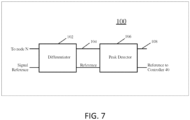
- a current sensor 100 which uses virtually no energy/power is disclosed.
- a differentiator circuit 102 has an input connected to node N (see FIG. 1 ).
- An output 104 of the differentiator 102 creates a signal D, which is proportional to the rate of change of voltage at node N. Because the impedance at node N is capacitive during the converter dead times, the signal at node N is proportional to the current flowing into node N during the dead times. Under the control of the controller 40, this signal D at output 104 is sampled during the dead times for a measure of inductor current, or fed to a peak detector 106 so as to measure the maximums or minimums automatically. The sampled signal at node 104 or peak-detected output signal at output 108 can then be used by the controller 40 of the power converter 20.
- FIG. 8 illustrates an exemplary low loss current sensor according to an aspect of the present invention.
- the differentiator 102 has been approximated by a high-pass filter composed of sensing capacitor C3 (typically 1pF-1nF) and resistor R1 (typically 100 ⁇ -10K ⁇ ), and the peak detector 106 has been implemented with diode D1 whose input is connected to the output 104, and detection capacitor C4 (typically 100pF-1nF) and switch S3 (which may be a MOSFET) connected in parallel to each other.
- the switch S3 is under the control of, or may be an integral part of the controller 40.
- S3 is closed to discharge detection capacitor C4, then opened by the controller 40. If output 108 feeds into a microcontroller, it may be possible for the microcontroller to hold the output node 108 low with an internal switch to discharge detection capacitor C4, thus eliminating the need for a separate switch S3.
- the full current of inductor L flows into node N, with a total capacitance of typically 1-1000nF, which includes the output capacitance Coss of the power switches S1 and S2 and the explicit capacitors C1 and C2 (see FIG. 1 ).
- Some small fraction of the inductor L current also flows through sensing capacitor C3, according to the ratio of C3 to the total capacitance at node N, which may typically be in the range of 1/100-1/10,000.
- This current is converted to a voltage by resistor R1, rectified by diode D1, and over several cycles, charges up detection capacitor C4 to a voltage equal to the peak value of output 104 less the voltage drop of diode D1 to produce a signal at output 108, which represents a measure of current flowing into the converter capacitors C1 and C2 through the inductor L during one of the dead times.
- the dead times typically occur at times of maximum and minimum inductor current.
- the invention may be configured to produce a measure of either the maximum or minimum (Ilmin) inductor current over the switching cycle.
- a typical method of measuring current involves passing the entire current through a resistor, which can be very lossy.
- the current sensor 100 of the present invention only about 1/1000th of the current is being passed through a resistor for only perhaps 1/100th of the time (the converter dead times). Therefore, the current sensor of FIG. 8 allows inductor L current to be sensed with extremely low power dissipation, e.g., on the order of 1/10,000th - 1/100,000th of the conventional technique.
- the differentiator circuit 102 has been shown with a high pass filter comprising capacitor C3 and resistor R1, other types of circuits can be used such as a resistor connected in series with an inductor between the switching node N and reference with the node common to the resistor and inductor being its output. Conventional active differentiators and peak detectors may also be employed.
- FIG. 9 illustrates representative waveforms of various nodes in the current sensor of FIG. 8 .
- the voltage 110 at node N alternates between 20 V and 0V.
- the current 112 flowing through the inductor L rises to approximately 11A when the switch S1 turns on and falls to approximately 0A when the switch S1 turns off and S2 turns on.
- the current through the inductor L falls below 0V to approximately -1. 5A before rising to 0A.
- the current sensor 100 can be configured to calculate either maximum or minimum current (negative or positive peak current) into a capacitive node by changing, for example, the orientation of the diode, it is preferred for use in the ZVS converter described herein to provide a measure of the minimum inductor current Ilmin.
- Ilmin can be calculated from the voltage V108 at output 108 of the current sensor 100 using the following equation, where M is a constant (negative in this example) dependent primarily on the circuit component values, and Vk is a constant voltage substantially equal to the diode drop of diode D1:
- Ilmin M* V108 + Vk
- Direct measurement of Ilmin allows the controller 40 to regulate T1 and T2 according to equations (6) and (7) so that Ilmin approaches the optimal value Ilmintarget.
- the controller 40 uses the sensed current at output 108 to control the power converter 20 for optimal charging of a battery at V2 from a power source at V1. Since the output 108 is an analog signal, it is routed to the A/D converter 16 of the controller to convert it to a digital signal. Often, the optimal input voltage at V1 for charging a battery at V2 changes according to the power being generated by, or other characteristics of, the power source at V1. For example, a power source such as a solar panel generates maximum power at a particular voltage which depends on various factors such as insolation, shading, dirt on the panel, temperature, age of the panel, and the like. That optimal voltage at any given time needs to be found for maximum transfer of power to the load at V2.
- the controller 40 can vary the high switch S1 on-time (T1) by a certain increment in one direction, e.g., gradually increasing T1 by a predetermined increment thereby gradually decreasing the voltage V1.
- the controller 40 monitors the output 108 to see if Ildc increases according to equation (15). If so, the controller 40 continues to increase T1 to reduce the voltage at V1 further to continue to "climb the hill" and increase Ildc. Assuming the battery voltage V2 is relatively constant, an increase in Ildc corresponds to an increase in power delivery from the solar panel to the battery.
- the controller 40 determines via monitoring output 108 that Ildc has decreased, it indicates that the power converter 20 went past the optimal voltage V1 and started to go "downhill" in power delivery. In that case, the controller 40 changes direction and starts to decrease the T1 by a second predetermined increment thereby gradually increasing the voltage V1.
- the second predetermined increment can be a smaller increment for fine tuning the proper T1.
- the decrease in T1 continues until power output decreases, at which point the controller will begin increasing T1, repeating the cycle.
- hill climbing is an iterative process and the controller 40 is continuously adjusting T1 to adjust for the changing power generation condition of the power source.
- controller 40 may be necessary for the controller 40 to adjust T2 (and T1 proportionally) to maintain Ilmin near Ilmintarget and thus ensure optimal electrical efficiency of the ZVS converter.
- the controller can directly compare the present voltage value (sampled values) at 108 to a previous voltage value at 108 to determine whether the current Ildc went up or down without any further calculation.
- adjustment of T1 and T2 for both optimal converter frequency and to implement a hill climbing algorithm may be accomplished without the need to calculate Ildc according to equation (15).
- the controller 40 samples the current from the current sensor 100 whenever the readings are needed. In another example, the controller 40 samples the current from the current sensor 100 at only the dead times, either 66, 68 (see FIG. 5 ) or both.
- the power converter 20 can be operated in a reverse direction to supply power to V1 from V2 simply by changing the direction of diode D1 in the peak detector 106 and adjusting the controller algorithm appropriately.
- Two current sensors may be used in order to produce a bidirectional power converter.
Landscapes
- Physics & Mathematics (AREA)
- Engineering & Computer Science (AREA)
- Power Engineering (AREA)
- General Physics & Mathematics (AREA)
- Nonlinear Science (AREA)
- Dc-Dc Converters (AREA)
Claims (6)
- Leistungswandler (20) aufweisend:erste und zweite Schalter (S1, S2), die in Reihe geschaltet sind und zwischen sich einen gemeinsamen Knoten (N) definieren;einen ersten und einen zweiten Schaltkreiskondensator (C1, C2), die parallel zu den ersten und zweiten Schaltern (S1, S2) geschaltet sind;eine Induktivität (L), die mit dem gemeinsamen Knoten (N) verbunden ist und dazu ausgepasst ist, eine Last mit Strom zu versorgen oder Strom von einem Eingang zu empfangen;einen verlustarmen Stromsensor (100), der dazu konfiguriert ist, einen in den gemeinsamen Knoten (N) fließenden Strom zu erfassen, und der eine Differenziererschaltung (102) aufweist, die einen mit dem ersten und dem zweiten Schaltungskondensator (C1, C2) verbundenen Eingang und einen Ausgang (104), der so ausgelegt ist, dass er am Ausgang (104) ein Ausgangssignal (D) erzeugt, das proportional zu dem durch den ersten und zweiten Schaltkreiskondensator (C1, C2) fließenden Strom ist, wobei die Differenziererschaltung (102) aufweist:einen Messkondensator (C3), der einen ersten Anschluss aufweist, der mit dem gemeinsamen Knoten (N) verbunden dazu ausgelegt ist, einen Ausgang zu erzeugen, der einen Strom führt, der proportional zu dem Strom ist, der durch den ersten und den zweiten Schaltkreiskondensator (C1, C2) fließt;einen Widerstand (R1), der mit einem zweiten Anschluss des Messkondensators (C3) verbunden ist und so konfiguriert ist, dass er einen Ausgang (104) des Stromsensors (100) definiert, wobei ein Spannungsabfall über dem Widerstand (R1) im Wesentlichen proportional zu dem durch den Messkondensator (C3) fließenden Strom ist;einen mit dem Widerstand (R1) verbundenen Spitzenwertdetektor (106) zum Erfassen eines Spitzenwerts des durch den ersten und zweiten Schaltkreiskondensator (C1, C2) fließenden Stroms,wobei der Spitzenwertdetektor (106) eine Diode (D1), die eine mit dem Widerstand (R1) verbundenen Eingang aufweist, und einen zwischen der Diode (D1) und einer Signalreferenz angeschlossenen Detektionskondensator (C4) umfasst, wobei die Spannung über dem Detektionskondensator (C4) einen erfassten Spitzenstromwert darstellt,eine Steuereinheit (40), die dazu ausgelegt ist, den ersten und den zweiten Schalter (S1, S2) auf komplementäre Weise zu schalten, um die Einschaltdauer von mindestens einem der ersten und zweiten Schalter (S1, S2) auf der Grundlage von Messwerten des Stromsensorausgangs (104) zu steuern, und die konfiguriert ist, das Ausgangssignal (D) am Ausgang (104) dem Spitzenwertdetektor (106) zuzuführen, um automatisch Maxima und Minima während der Totzeiten des ersten und zweiten Schalters (S1, S2) für eine Messung des Induktorstroms zu messen,wobei der Spitzenwertdetektor (106) ferner einen Schalter (S3) umfasst, der über den Detektionskondensator (C4) geschaltet ist,wobei die Steuereinheit (40) konfiguriert ist, eine Spannung über den Detektionskondensator (C4) abzutasten und den Schalter (S3) zu schließen, um den Detektionskondensator (C4) zu entladen und den Schalter (S3) vor dem Abtasten der Spannung zu öffnen.
- Leistungswandler nach Anspruch 1, wobei die Steuereinheit (40) dazu ausgelegt ist, einen optimalen Energieübertragungspunkt durch Variieren der Einschaltzeit von mindestens einem der ersten und zweiten Schalter (S1, S2) und durch Vergleichen entsprechender Werte des Stromsensorausgangs (104, 108) zu bestimmen.
- Leistungswandler nach Anspruch 1 oder 2, wobei die Kapazität des Messkondensators (C3) höchstens ein Prozent der Kapazität des ersten und zweiten Schaltkreiskondensators (C1, C2) beträgt.
- Leistungswandler nach Anspruch 1, wobei die Steuereinheit (40) dazu ausgelegt ist, eine Schaltfrequenz des ersten und zweiten Schalters (S1, S2) auf der Grundlage von Messwerten des Stromsensorausgangs (104, 108) dynamisch und kontinuierlich zu variieren.
- Leistungswandler nach Anspruch 1, wobei die Steuereinheit (40) das Ausgangssignal (108) des Stromsensors in digitale Werte umwandelt und die abgetasteten digitalen Werte abtastet.
- Leistungswandler nach Anspruch 1, wobei die Steuereinheit (40) die Einschaltzeit von mindestens einem der ersten und zweiten Schalter (S1, S2) auf der Grundlage eines direkten Vergleichs eines aktuellen Werts der Spannung über dem Erfassungskondensator (C4) und eines vorherigen Werts der Spannung über dem Erfassungskondensator (C4) ohne weitere Berechnung variiert.
Applications Claiming Priority (3)
| Application Number | Priority Date | Filing Date | Title |
|---|---|---|---|
| US201562200194P | 2015-08-03 | 2015-08-03 | |
| US15/226,468 US9759750B2 (en) | 2015-08-03 | 2016-08-02 | Low loss current sensor and power converter using the same |
| PCT/US2016/045264 WO2017023982A1 (en) | 2015-08-03 | 2016-08-03 | Low loss current sensor and power converter using the same |
Publications (3)
| Publication Number | Publication Date |
|---|---|
| EP3332260A1 EP3332260A1 (de) | 2018-06-13 |
| EP3332260A4 EP3332260A4 (de) | 2019-04-17 |
| EP3332260B1 true EP3332260B1 (de) | 2024-11-13 |
Family
ID=57943601
Family Applications (1)
| Application Number | Title | Priority Date | Filing Date |
|---|---|---|---|
| EP16833767.3A Active EP3332260B1 (de) | 2015-08-03 | 2016-08-03 | Verlustarmer stromsensor und leistungswandler damit |
Country Status (4)
| Country | Link |
|---|---|
| US (1) | US9759750B2 (de) |
| EP (1) | EP3332260B1 (de) |
| CA (1) | CA2992621C (de) |
| WO (1) | WO2017023982A1 (de) |
Families Citing this family (11)
| Publication number | Priority date | Publication date | Assignee | Title |
|---|---|---|---|---|
| FR3050336B1 (fr) * | 2016-04-15 | 2018-05-04 | Continental Automotive France | Procede de diagnostic de la commande en courant d'un moteur electrique d'un vehicule automobile |
| US10181847B2 (en) | 2017-02-01 | 2019-01-15 | Texas Instruments Incorporated | Ring amplitude measurement and mitigation |
| US10594315B2 (en) * | 2017-02-01 | 2020-03-17 | Texas Instruments Incorporated | Switching rate monitoring and control |
| FR3068844B1 (fr) * | 2017-07-10 | 2022-05-13 | Exagan | Dispositif electronique en demi-pont comprenant deux systemes pour la minimisation des temps morts entre les commutations d'un interrupteur niveau haut et d'un interrupteur niveau bas. |
| DE112018007167A5 (de) | 2018-02-27 | 2020-12-10 | Siemens Aktiengesellschaft | Halbbrücke mit Leistungshalbleitern |
| US11121704B2 (en) | 2018-04-23 | 2021-09-14 | Texas Instruments Incorporated | Parallelling multiple power switches |
| FR3081633B1 (fr) * | 2018-05-22 | 2021-06-18 | Exagan | Dispositif electronique en demi-pont comprenant deux systemes pour l'optimisation des temps morts entre les commutations d'un interrupteur niveau haut et d'un interrupteur niveau bas |
| US10673432B1 (en) * | 2018-12-13 | 2020-06-02 | Texas Instruments Incorporated | Delaying turn on time to transistor comparing global, peak current |
| FI129607B (en) * | 2021-05-18 | 2022-05-31 | Vensum Power Oy | System and method for zero voltage switching in a power converter |
| DE102022129779B4 (de) | 2022-11-10 | 2024-10-10 | Friedrich-Alexander-Universität Erlangen-Nürnberg, Körperschaft des öffentlichen Rechts | Verfahren zur Ermittlung des Stroms beim Nullspannungsschalten |
| US20240178746A1 (en) * | 2022-11-29 | 2024-05-30 | Qorvo Us, Inc. | Adaptive dead-time control for switching circuitry of a dc converter |
Citations (3)
| Publication number | Priority date | Publication date | Assignee | Title |
|---|---|---|---|---|
| US4373141A (en) * | 1981-01-22 | 1983-02-08 | E-Systems, Inc. | Fast updating peak detector circuit |
| EP1903652A2 (de) * | 2006-09-21 | 2008-03-26 | LuK Lamellen und Kupplungsbau Beteiligungs KG | Verfahren und Schaltung zum Bestimmen des maximalen, von einem Elektromotor aufgenommenen Stroms |
| US20110163992A1 (en) * | 2010-01-05 | 2011-07-07 | 3M Innovative Properties Company | High speed noise tolerant multi-touch touch device and controller therefor |
Family Cites Families (14)
| Publication number | Priority date | Publication date | Assignee | Title |
|---|---|---|---|---|
| US3072805A (en) * | 1958-11-13 | 1963-01-08 | Acoustica Associates Inc | Autopolarization of electrostrictive transducers |
| JP3249380B2 (ja) | 1995-06-13 | 2002-01-21 | 株式会社東芝 | 電力変換装置 |
| JP3477923B2 (ja) * | 1995-06-29 | 2003-12-10 | 三菱電機株式会社 | 内燃機関用燃焼状態検知装置 |
| US5684688A (en) | 1996-06-24 | 1997-11-04 | Reliance Electric Industrial Company | Soft switching three-level inverter |
| US6002922A (en) * | 1996-12-17 | 1999-12-14 | Motorola, Inc. | Method and apparatus for detecting communication signals |
| US5982160A (en) * | 1998-12-24 | 1999-11-09 | Harris Corporation | DC-to-DC converter with inductor current sensing and related methods |
| US6429638B1 (en) | 2000-08-31 | 2002-08-06 | Nortel Networks Limited | N-diode peak detector |
| EP1771937A1 (de) * | 2004-07-21 | 2007-04-11 | Koninklijke Philips Electronics N.V. | Automatische frequenzregelung für ein reihenresonanz-schaltnetzteil |
| US9203300B2 (en) | 2009-05-20 | 2015-12-01 | Alex Mevay | Systems and methods for controlling power converters |
| TWI429165B (zh) * | 2011-02-01 | 2014-03-01 | 富達通科技股份有限公司 | Method of data transmission in high power induction power supply |
| WO2012101906A1 (ja) | 2011-01-26 | 2012-08-02 | 株式会社村田製作所 | スイッチング電源装置 |
| US8941267B2 (en) * | 2011-06-07 | 2015-01-27 | Fu Da Tong Technology Co., Ltd. | High-power induction-type power supply system and its bi-phase decoding method |
| US8780590B2 (en) | 2012-05-03 | 2014-07-15 | Hong Kong Applied Science & Technology Research Institute Company, Ltd. | Output current estimation for an isolated flyback converter with variable switching frequency control and duty cycle adjustment for both PWM and PFM modes |
| KR102045780B1 (ko) | 2013-03-05 | 2019-11-18 | 삼성전자주식회사 | 양방향 전압 배치 회로, 이를 포함하는 전압 컨버터 및 전력 공급 장치 |
-
2016
- 2016-08-02 US US15/226,468 patent/US9759750B2/en active Active
- 2016-08-03 EP EP16833767.3A patent/EP3332260B1/de active Active
- 2016-08-03 WO PCT/US2016/045264 patent/WO2017023982A1/en not_active Ceased
- 2016-08-03 CA CA2992621A patent/CA2992621C/en active Active
Patent Citations (3)
| Publication number | Priority date | Publication date | Assignee | Title |
|---|---|---|---|---|
| US4373141A (en) * | 1981-01-22 | 1983-02-08 | E-Systems, Inc. | Fast updating peak detector circuit |
| EP1903652A2 (de) * | 2006-09-21 | 2008-03-26 | LuK Lamellen und Kupplungsbau Beteiligungs KG | Verfahren und Schaltung zum Bestimmen des maximalen, von einem Elektromotor aufgenommenen Stroms |
| US20110163992A1 (en) * | 2010-01-05 | 2011-07-07 | 3M Innovative Properties Company | High speed noise tolerant multi-touch touch device and controller therefor |
Non-Patent Citations (1)
| Title |
|---|
| "Operational Amplifiers Chapter 6", 31 December 2003, NEWNES, https://nvhrbiblio.nl/biblio/boek/Clayton%20-%20Operational%20Amplifiers.pdf, ISBN: 978-0-7506-5914-7, article GEORGE CLAYTON: "Operational Amplifiers Chapter 6", pages: 163 - 169, XP055689105 * |
Also Published As
| Publication number | Publication date |
|---|---|
| EP3332260A4 (de) | 2019-04-17 |
| US9759750B2 (en) | 2017-09-12 |
| CA2992621A1 (en) | 2017-02-09 |
| US20170040894A1 (en) | 2017-02-09 |
| CA2992621C (en) | 2019-06-18 |
| EP3332260A1 (de) | 2018-06-13 |
| WO2017023982A1 (en) | 2017-02-09 |
Similar Documents
| Publication | Publication Date | Title |
|---|---|---|
| EP3332260B1 (de) | Verlustarmer stromsensor und leistungswandler damit | |
| EP1687683B1 (de) | Adaptive verzögerungsregelschaltung für ein schaltnetzteil | |
| US10263518B2 (en) | System and method for switched power supply with delay measurement | |
| US8395362B2 (en) | Controlling a dead time of a switching voltage regulator | |
| US6377032B1 (en) | Method and apparatus for virtual current sensing in DC-DC switched mode power supplies | |
| US8810229B2 (en) | DC/DC converter | |
| US7196503B2 (en) | Current averaging circuit for a PWM power converter | |
| US8648583B2 (en) | Delay block for controlling a dead time of a switching voltage regulator | |
| US10389237B1 (en) | Light-load efficiency improvement of hybrid switched capacitor converter | |
| US9203301B2 (en) | Feedback for controlling the switching frequency of a voltage regulator | |
| US7456620B2 (en) | Determining dead times in switched-mode DC-DC converters | |
| TWI437808B (zh) | A system and method for dynamic threshold adjustment of a flyback power converter | |
| EP2999107A1 (de) | Energiegewinnungsschaltung und Verfahren | |
| US9979271B2 (en) | Power converter with zero-voltage switching control | |
| EP2515426A1 (de) | Schaltkreis | |
| CN109997301A (zh) | 用于dc-dc电力转换器的控制方案 | |
| US10126792B2 (en) | Power converter load current control | |
| KR20120092524A (ko) | 고정 오프 타임 부스트 컨버터 | |
| CN112311233A (zh) | 在恒定导通时间调节器中测量电流 | |
| US20210099092A1 (en) | Methods and systems of operating power converters | |
| US10181843B2 (en) | Adaptive control of the non-overlap time of power switches | |
| US8836299B2 (en) | Voltage converter | |
| CN110311557B (zh) | 直流-直流转换控制器及其运作方法 | |
| US20190181759A1 (en) | Buck-boost power converter controller | |
| JP2001136738A (ja) | スイッチングdc−dcコンバータ用制御回路 |
Legal Events
| Date | Code | Title | Description |
|---|---|---|---|
| STAA | Information on the status of an ep patent application or granted ep patent |
Free format text: STATUS: THE INTERNATIONAL PUBLICATION HAS BEEN MADE |
|
| PUAI | Public reference made under article 153(3) epc to a published international application that has entered the european phase |
Free format text: ORIGINAL CODE: 0009012 |
|
| STAA | Information on the status of an ep patent application or granted ep patent |
Free format text: STATUS: REQUEST FOR EXAMINATION WAS MADE |
|
| 17P | Request for examination filed |
Effective date: 20180302 |
|
| AK | Designated contracting states |
Kind code of ref document: A1 Designated state(s): AL AT BE BG CH CY CZ DE DK EE ES FI FR GB GR HR HU IE IS IT LI LT LU LV MC MK MT NL NO PL PT RO RS SE SI SK SM TR |
|
| AX | Request for extension of the european patent |
Extension state: BA ME |
|
| DAV | Request for validation of the european patent (deleted) | ||
| DAX | Request for extension of the european patent (deleted) | ||
| RAP1 | Party data changed (applicant data changed or rights of an application transferred) |
Owner name: SUNFORGE LLC |
|
| RIN1 | Information on inventor provided before grant (corrected) |
Inventor name: SUNFORGE LLC |
|
| A4 | Supplementary search report drawn up and despatched |
Effective date: 20190319 |
|
| RIC1 | Information provided on ipc code assigned before grant |
Ipc: G01R 19/04 20060101ALN20190313BHEP Ipc: H03K 5/1532 20060101ALN20190313BHEP Ipc: H02M 1/38 20070101ALI20190313BHEP Ipc: H02M 1/00 20060101ALI20190313BHEP Ipc: G01R 15/16 20060101ALN20190313BHEP Ipc: H02M 3/158 20060101AFI20190313BHEP |
|
| STAA | Information on the status of an ep patent application or granted ep patent |
Free format text: STATUS: EXAMINATION IS IN PROGRESS |
|
| 17Q | First examination report despatched |
Effective date: 20200122 |
|
| REG | Reference to a national code |
Ref country code: DE Ref legal event code: R079 Free format text: PREVIOUS MAIN CLASS: G01R0019000000 Ipc: H02M0003158000 Ref country code: DE Ref legal event code: R079 Ref document number: 602016090256 Country of ref document: DE Free format text: PREVIOUS MAIN CLASS: G01R0019000000 Ipc: H02M0003158000 |
|
| GRAP | Despatch of communication of intention to grant a patent |
Free format text: ORIGINAL CODE: EPIDOSNIGR1 |
|
| STAA | Information on the status of an ep patent application or granted ep patent |
Free format text: STATUS: GRANT OF PATENT IS INTENDED |
|
| RIC1 | Information provided on ipc code assigned before grant |
Ipc: H03K 5/1532 20060101ALN20220208BHEP Ipc: G01R 15/16 20060101ALN20220208BHEP Ipc: G01R 19/04 20060101ALN20220208BHEP Ipc: G01R 31/42 20060101ALI20220208BHEP Ipc: G01R 19/00 20060101ALI20220208BHEP Ipc: H02M 1/00 20060101ALI20220208BHEP Ipc: H02M 1/38 20070101ALI20220208BHEP Ipc: H02M 3/158 20060101AFI20220208BHEP |
|
| INTG | Intention to grant announced |
Effective date: 20220225 |
|
| RIC1 | Information provided on ipc code assigned before grant |
Ipc: H03K 5/1532 20060101ALN20220211BHEP Ipc: G01R 15/16 20060101ALN20220211BHEP Ipc: G01R 19/04 20060101ALN20220211BHEP Ipc: G01R 31/42 20060101ALI20220211BHEP Ipc: G01R 19/00 20060101ALI20220211BHEP Ipc: H02M 1/00 20060101ALI20220211BHEP Ipc: H02M 1/38 20070101ALI20220211BHEP Ipc: H02M 3/158 20060101AFI20220211BHEP |
|
| GRAS | Grant fee paid |
Free format text: ORIGINAL CODE: EPIDOSNIGR3 |
|
| GRAJ | Information related to disapproval of communication of intention to grant by the applicant or resumption of examination proceedings by the epo deleted |
Free format text: ORIGINAL CODE: EPIDOSDIGR1 |
|
| GRAL | Information related to payment of fee for publishing/printing deleted |
Free format text: ORIGINAL CODE: EPIDOSDIGR3 |
|
| STAA | Information on the status of an ep patent application or granted ep patent |
Free format text: STATUS: EXAMINATION IS IN PROGRESS |
|
| RIN1 | Information on inventor provided before grant (corrected) |
Inventor name: MEVAY, ALEX C.H. |
|
| INTC | Intention to grant announced (deleted) | ||
| P01 | Opt-out of the competence of the unified patent court (upc) registered |
Effective date: 20230528 |
|
| GRAP | Despatch of communication of intention to grant a patent |
Free format text: ORIGINAL CODE: EPIDOSNIGR1 |
|
| STAA | Information on the status of an ep patent application or granted ep patent |
Free format text: STATUS: GRANT OF PATENT IS INTENDED |
|
| RIC1 | Information provided on ipc code assigned before grant |
Ipc: H03K 5/1532 20060101ALN20240207BHEP Ipc: G01R 15/16 20060101ALN20240207BHEP Ipc: G01R 19/04 20060101ALN20240207BHEP Ipc: G01R 31/42 20060101ALI20240207BHEP Ipc: G01R 19/00 20060101ALI20240207BHEP Ipc: H02M 1/00 20060101ALI20240207BHEP Ipc: H02M 1/38 20070101ALI20240207BHEP Ipc: H02M 3/158 20060101AFI20240207BHEP |
|
| INTG | Intention to grant announced |
Effective date: 20240221 |
|
| GRAJ | Information related to disapproval of communication of intention to grant by the applicant or resumption of examination proceedings by the epo deleted |
Free format text: ORIGINAL CODE: EPIDOSDIGR1 |
|
| STAA | Information on the status of an ep patent application or granted ep patent |
Free format text: STATUS: EXAMINATION IS IN PROGRESS |
|
| RAP3 | Party data changed (applicant data changed or rights of an application transferred) |
Owner name: SUNFORGE LLC |
|
| GRAP | Despatch of communication of intention to grant a patent |
Free format text: ORIGINAL CODE: EPIDOSNIGR1 |
|
| STAA | Information on the status of an ep patent application or granted ep patent |
Free format text: STATUS: GRANT OF PATENT IS INTENDED |
|
| INTC | Intention to grant announced (deleted) | ||
| INTG | Intention to grant announced |
Effective date: 20240607 |
|
| RIC1 | Information provided on ipc code assigned before grant |
Ipc: H03K 5/1532 20060101ALN20240527BHEP Ipc: G01R 15/16 20060101ALN20240527BHEP Ipc: G01R 19/04 20060101ALN20240527BHEP Ipc: G01R 31/42 20060101ALI20240527BHEP Ipc: G01R 19/00 20060101ALI20240527BHEP Ipc: H02M 1/00 20060101ALI20240527BHEP Ipc: H02M 1/38 20070101ALI20240527BHEP Ipc: H02M 3/158 20060101AFI20240527BHEP |
|
| GRAS | Grant fee paid |
Free format text: ORIGINAL CODE: EPIDOSNIGR3 |
|
| GRAA | (expected) grant |
Free format text: ORIGINAL CODE: 0009210 |
|
| STAA | Information on the status of an ep patent application or granted ep patent |
Free format text: STATUS: THE PATENT HAS BEEN GRANTED |
|
| AK | Designated contracting states |
Kind code of ref document: B1 Designated state(s): AL AT BE BG CH CY CZ DE DK EE ES FI FR GB GR HR HU IE IS IT LI LT LU LV MC MK MT NL NO PL PT RO RS SE SI SK SM TR |
|
| REG | Reference to a national code |
Ref country code: GB Ref legal event code: FG4D |
|
| REG | Reference to a national code |
Ref country code: CH Ref legal event code: EP |
|
| REG | Reference to a national code |
Ref country code: IE Ref legal event code: FG4D |
|
| REG | Reference to a national code |
Ref country code: DE Ref legal event code: R096 Ref document number: 602016090256 Country of ref document: DE |
|
| REG | Reference to a national code |
Ref country code: NL Ref legal event code: FP |
|
| REG | Reference to a national code |
Ref country code: LT Ref legal event code: MG9D |
|
| PG25 | Lapsed in a contracting state [announced via postgrant information from national office to epo] |
Ref country code: PT Free format text: LAPSE BECAUSE OF FAILURE TO SUBMIT A TRANSLATION OF THE DESCRIPTION OR TO PAY THE FEE WITHIN THE PRESCRIBED TIME-LIMIT Effective date: 20250313 Ref country code: IS Free format text: LAPSE BECAUSE OF FAILURE TO SUBMIT A TRANSLATION OF THE DESCRIPTION OR TO PAY THE FEE WITHIN THE PRESCRIBED TIME-LIMIT Effective date: 20250313 Ref country code: HR Free format text: LAPSE BECAUSE OF FAILURE TO SUBMIT A TRANSLATION OF THE DESCRIPTION OR TO PAY THE FEE WITHIN THE PRESCRIBED TIME-LIMIT Effective date: 20241113 |
|
| PG25 | Lapsed in a contracting state [announced via postgrant information from national office to epo] |
Ref country code: FI Free format text: LAPSE BECAUSE OF FAILURE TO SUBMIT A TRANSLATION OF THE DESCRIPTION OR TO PAY THE FEE WITHIN THE PRESCRIBED TIME-LIMIT Effective date: 20241113 |
|
| REG | Reference to a national code |
Ref country code: AT Ref legal event code: MK05 Ref document number: 1742432 Country of ref document: AT Kind code of ref document: T Effective date: 20241113 |
|
| PG25 | Lapsed in a contracting state [announced via postgrant information from national office to epo] |
Ref country code: BG Free format text: LAPSE BECAUSE OF FAILURE TO SUBMIT A TRANSLATION OF THE DESCRIPTION OR TO PAY THE FEE WITHIN THE PRESCRIBED TIME-LIMIT Effective date: 20241113 |
|
| PG25 | Lapsed in a contracting state [announced via postgrant information from national office to epo] |
Ref country code: ES Free format text: LAPSE BECAUSE OF FAILURE TO SUBMIT A TRANSLATION OF THE DESCRIPTION OR TO PAY THE FEE WITHIN THE PRESCRIBED TIME-LIMIT Effective date: 20241113 |
|
| PG25 | Lapsed in a contracting state [announced via postgrant information from national office to epo] |
Ref country code: NO Free format text: LAPSE BECAUSE OF FAILURE TO SUBMIT A TRANSLATION OF THE DESCRIPTION OR TO PAY THE FEE WITHIN THE PRESCRIBED TIME-LIMIT Effective date: 20250213 |
|
| PG25 | Lapsed in a contracting state [announced via postgrant information from national office to epo] |
Ref country code: LV Free format text: LAPSE BECAUSE OF FAILURE TO SUBMIT A TRANSLATION OF THE DESCRIPTION OR TO PAY THE FEE WITHIN THE PRESCRIBED TIME-LIMIT Effective date: 20241113 Ref country code: AT Free format text: LAPSE BECAUSE OF FAILURE TO SUBMIT A TRANSLATION OF THE DESCRIPTION OR TO PAY THE FEE WITHIN THE PRESCRIBED TIME-LIMIT Effective date: 20241113 Ref country code: GR Free format text: LAPSE BECAUSE OF FAILURE TO SUBMIT A TRANSLATION OF THE DESCRIPTION OR TO PAY THE FEE WITHIN THE PRESCRIBED TIME-LIMIT Effective date: 20250214 |
|
| PG25 | Lapsed in a contracting state [announced via postgrant information from national office to epo] |
Ref country code: PL Free format text: LAPSE BECAUSE OF FAILURE TO SUBMIT A TRANSLATION OF THE DESCRIPTION OR TO PAY THE FEE WITHIN THE PRESCRIBED TIME-LIMIT Effective date: 20241113 |
|
| PG25 | Lapsed in a contracting state [announced via postgrant information from national office to epo] |
Ref country code: RS Free format text: LAPSE BECAUSE OF FAILURE TO SUBMIT A TRANSLATION OF THE DESCRIPTION OR TO PAY THE FEE WITHIN THE PRESCRIBED TIME-LIMIT Effective date: 20250213 |
|
| PG25 | Lapsed in a contracting state [announced via postgrant information from national office to epo] |
Ref country code: SM Free format text: LAPSE BECAUSE OF FAILURE TO SUBMIT A TRANSLATION OF THE DESCRIPTION OR TO PAY THE FEE WITHIN THE PRESCRIBED TIME-LIMIT Effective date: 20241113 |
|
| PG25 | Lapsed in a contracting state [announced via postgrant information from national office to epo] |
Ref country code: DK Free format text: LAPSE BECAUSE OF FAILURE TO SUBMIT A TRANSLATION OF THE DESCRIPTION OR TO PAY THE FEE WITHIN THE PRESCRIBED TIME-LIMIT Effective date: 20241113 |
|
| PG25 | Lapsed in a contracting state [announced via postgrant information from national office to epo] |
Ref country code: EE Free format text: LAPSE BECAUSE OF FAILURE TO SUBMIT A TRANSLATION OF THE DESCRIPTION OR TO PAY THE FEE WITHIN THE PRESCRIBED TIME-LIMIT Effective date: 20241113 |
|
| PG25 | Lapsed in a contracting state [announced via postgrant information from national office to epo] |
Ref country code: RO Free format text: LAPSE BECAUSE OF FAILURE TO SUBMIT A TRANSLATION OF THE DESCRIPTION OR TO PAY THE FEE WITHIN THE PRESCRIBED TIME-LIMIT Effective date: 20241113 |
|
| PG25 | Lapsed in a contracting state [announced via postgrant information from national office to epo] |
Ref country code: SK Free format text: LAPSE BECAUSE OF FAILURE TO SUBMIT A TRANSLATION OF THE DESCRIPTION OR TO PAY THE FEE WITHIN THE PRESCRIBED TIME-LIMIT Effective date: 20241113 |
|
| PG25 | Lapsed in a contracting state [announced via postgrant information from national office to epo] |
Ref country code: CZ Free format text: LAPSE BECAUSE OF FAILURE TO SUBMIT A TRANSLATION OF THE DESCRIPTION OR TO PAY THE FEE WITHIN THE PRESCRIBED TIME-LIMIT Effective date: 20241113 |
|
| REG | Reference to a national code |
Ref country code: DE Ref legal event code: R097 Ref document number: 602016090256 Country of ref document: DE |
|
| PG25 | Lapsed in a contracting state [announced via postgrant information from national office to epo] |
Ref country code: SE Free format text: LAPSE BECAUSE OF FAILURE TO SUBMIT A TRANSLATION OF THE DESCRIPTION OR TO PAY THE FEE WITHIN THE PRESCRIBED TIME-LIMIT Effective date: 20241113 |
|
| PGFP | Annual fee paid to national office [announced via postgrant information from national office to epo] |
Ref country code: NL Payment date: 20250826 Year of fee payment: 10 |
|
| PLBE | No opposition filed within time limit |
Free format text: ORIGINAL CODE: 0009261 |
|
| STAA | Information on the status of an ep patent application or granted ep patent |
Free format text: STATUS: NO OPPOSITION FILED WITHIN TIME LIMIT |
|
| PGFP | Annual fee paid to national office [announced via postgrant information from national office to epo] |
Ref country code: DE Payment date: 20250827 Year of fee payment: 10 |
|
| PGFP | Annual fee paid to national office [announced via postgrant information from national office to epo] |
Ref country code: IT Payment date: 20250820 Year of fee payment: 10 |
|
| PGFP | Annual fee paid to national office [announced via postgrant information from national office to epo] |
Ref country code: GB Payment date: 20250827 Year of fee payment: 10 |
|
| 26N | No opposition filed |
Effective date: 20250814 |
|
| REG | Reference to a national code |
Ref country code: CH Ref legal event code: H13 Free format text: ST27 STATUS EVENT CODE: U-0-0-H10-H13 (AS PROVIDED BY THE NATIONAL OFFICE) Effective date: 20260324 |
|
| PG25 | Lapsed in a contracting state [announced via postgrant information from national office to epo] |
Ref country code: MC Free format text: LAPSE BECAUSE OF FAILURE TO SUBMIT A TRANSLATION OF THE DESCRIPTION OR TO PAY THE FEE WITHIN THE PRESCRIBED TIME-LIMIT Effective date: 20241113 |
|
| PG25 | Lapsed in a contracting state [announced via postgrant information from national office to epo] |
Ref country code: LU Free format text: LAPSE BECAUSE OF NON-PAYMENT OF DUE FEES Effective date: 20250803 |
|
| PG25 | Lapsed in a contracting state [announced via postgrant information from national office to epo] |
Ref country code: CH Free format text: LAPSE BECAUSE OF NON-PAYMENT OF DUE FEES Effective date: 20250831 |