EP3333986B1 - Elektronisches bauteil und abbildungsvorrichtung - Google Patents
Elektronisches bauteil und abbildungsvorrichtung Download PDFInfo
- Publication number
- EP3333986B1 EP3333986B1 EP17204303.6A EP17204303A EP3333986B1 EP 3333986 B1 EP3333986 B1 EP 3333986B1 EP 17204303 A EP17204303 A EP 17204303A EP 3333986 B1 EP3333986 B1 EP 3333986B1
- Authority
- EP
- European Patent Office
- Prior art keywords
- connector
- electronic component
- external conductor
- case portion
- external
- Prior art date
- Legal status (The legal status is an assumption and is not a legal conclusion. Google has not performed a legal analysis and makes no representation as to the accuracy of the status listed.)
- Active
Links
Images


Classifications
-
- H—ELECTRICITY
- H04—ELECTRIC COMMUNICATION TECHNIQUE
- H04N—PICTORIAL COMMUNICATION, e.g. TELEVISION
- H04N23/00—Cameras or camera modules comprising electronic image sensors; Control thereof
- H04N23/50—Constructional details
- H04N23/51—Housings
-
- H—ELECTRICITY
- H10—SEMICONDUCTOR DEVICES; ELECTRIC SOLID-STATE DEVICES NOT OTHERWISE PROVIDED FOR
- H10F—INORGANIC SEMICONDUCTOR DEVICES SENSITIVE TO INFRARED RADIATION, LIGHT, ELECTROMAGNETIC RADIATION OF SHORTER WAVELENGTH OR CORPUSCULAR RADIATION
- H10F39/00—Integrated devices, or assemblies of multiple devices, comprising at least one element covered by group H10F30/00, e.g. radiation detectors comprising photodiode arrays
- H10F39/80—Constructional details of image sensors
- H10F39/804—Containers or encapsulations
-
- H—ELECTRICITY
- H01—ELECTRIC ELEMENTS
- H01R—ELECTRICALLY-CONDUCTIVE CONNECTIONS; STRUCTURAL ASSOCIATIONS OF A PLURALITY OF MUTUALLY-INSULATED ELECTRICAL CONNECTING ELEMENTS; COUPLING DEVICES; CURRENT COLLECTORS
- H01R13/00—Details of coupling devices of the kinds covered by groups H01R12/70 or H01R24/00 - H01R33/00
- H01R13/40—Securing contact members in or to a base or case; Insulating of contact members
-
- H—ELECTRICITY
- H01—ELECTRIC ELEMENTS
- H01R—ELECTRICALLY-CONDUCTIVE CONNECTIONS; STRUCTURAL ASSOCIATIONS OF A PLURALITY OF MUTUALLY-INSULATED ELECTRICAL CONNECTING ELEMENTS; COUPLING DEVICES; CURRENT COLLECTORS
- H01R13/00—Details of coupling devices of the kinds covered by groups H01R12/70 or H01R24/00 - H01R33/00
- H01R13/46—Bases; Cases
-
- H—ELECTRICITY
- H01—ELECTRIC ELEMENTS
- H01R—ELECTRICALLY-CONDUCTIVE CONNECTIONS; STRUCTURAL ASSOCIATIONS OF A PLURALITY OF MUTUALLY-INSULATED ELECTRICAL CONNECTING ELEMENTS; COUPLING DEVICES; CURRENT COLLECTORS
- H01R13/00—Details of coupling devices of the kinds covered by groups H01R12/70 or H01R24/00 - H01R33/00
- H01R13/46—Bases; Cases
- H01R13/502—Bases; Cases composed of different pieces
- H01R13/504—Bases; Cases composed of different pieces different pieces being moulded, cemented, welded, e.g. ultrasonic welding, or swaged together
-
- H—ELECTRICITY
- H01—ELECTRIC ELEMENTS
- H01R—ELECTRICALLY-CONDUCTIVE CONNECTIONS; STRUCTURAL ASSOCIATIONS OF A PLURALITY OF MUTUALLY-INSULATED ELECTRICAL CONNECTING ELEMENTS; COUPLING DEVICES; CURRENT COLLECTORS
- H01R13/00—Details of coupling devices of the kinds covered by groups H01R12/70 or H01R24/00 - H01R33/00
- H01R13/648—Protective earth or shield arrangements on coupling devices, e.g. anti-static shielding
- H01R13/658—High frequency shielding arrangements, e.g. against EMI [Electro-Magnetic Interference] or EMP [Electro-Magnetic Pulse]
- H01R13/6581—Shield structure
-
- H—ELECTRICITY
- H04—ELECTRIC COMMUNICATION TECHNIQUE
- H04N—PICTORIAL COMMUNICATION, e.g. TELEVISION
- H04N23/00—Cameras or camera modules comprising electronic image sensors; Control thereof
- H04N23/50—Constructional details
-
- H—ELECTRICITY
- H05—ELECTRIC TECHNIQUES NOT OTHERWISE PROVIDED FOR
- H05K—PRINTED CIRCUITS; CASINGS OR CONSTRUCTIONAL DETAILS OF ELECTRIC APPARATUS; MANUFACTURE OF ASSEMBLAGES OF ELECTRICAL COMPONENTS
- H05K7/00—Constructional details common to different types of electric apparatus
- H05K7/20—Modifications to facilitate cooling, ventilating, or heating
- H05K7/2039—Modifications to facilitate cooling, ventilating, or heating characterised by the heat transfer by conduction from the heat generating element to a dissipating body
-
- H—ELECTRICITY
- H05—ELECTRIC TECHNIQUES NOT OTHERWISE PROVIDED FOR
- H05K—PRINTED CIRCUITS; CASINGS OR CONSTRUCTIONAL DETAILS OF ELECTRIC APPARATUS; MANUFACTURE OF ASSEMBLAGES OF ELECTRICAL COMPONENTS
- H05K7/00—Constructional details common to different types of electric apparatus
- H05K7/20—Modifications to facilitate cooling, ventilating, or heating
- H05K7/20845—Modifications to facilitate cooling, ventilating, or heating for automotive electronic casings
- H05K7/20854—Heat transfer by conduction from internal heat source to heat radiating structure
-
- H—ELECTRICITY
- H05—ELECTRIC TECHNIQUES NOT OTHERWISE PROVIDED FOR
- H05K—PRINTED CIRCUITS; CASINGS OR CONSTRUCTIONAL DETAILS OF ELECTRIC APPARATUS; MANUFACTURE OF ASSEMBLAGES OF ELECTRICAL COMPONENTS
- H05K9/00—Screening of apparatus or components against electric or magnetic fields
- H05K9/0007—Casings
-
- H—ELECTRICITY
- H05—ELECTRIC TECHNIQUES NOT OTHERWISE PROVIDED FOR
- H05K—PRINTED CIRCUITS; CASINGS OR CONSTRUCTIONAL DETAILS OF ELECTRIC APPARATUS; MANUFACTURE OF ASSEMBLAGES OF ELECTRICAL COMPONENTS
- H05K9/00—Screening of apparatus or components against electric or magnetic fields
- H05K9/0007—Casings
- H05K9/0049—Casings being metallic containers
-
- H—ELECTRICITY
- H01—ELECTRIC ELEMENTS
- H01R—ELECTRICALLY-CONDUCTIVE CONNECTIONS; STRUCTURAL ASSOCIATIONS OF A PLURALITY OF MUTUALLY-INSULATED ELECTRICAL CONNECTING ELEMENTS; COUPLING DEVICES; CURRENT COLLECTORS
- H01R13/00—Details of coupling devices of the kinds covered by groups H01R12/70 or H01R24/00 - H01R33/00
- H01R13/40—Securing contact members in or to a base or case; Insulating of contact members
- H01R13/405—Securing in non-demountable manner, e.g. moulding, riveting
-
- H—ELECTRICITY
- H01—ELECTRIC ELEMENTS
- H01R—ELECTRICALLY-CONDUCTIVE CONNECTIONS; STRUCTURAL ASSOCIATIONS OF A PLURALITY OF MUTUALLY-INSULATED ELECTRICAL CONNECTING ELEMENTS; COUPLING DEVICES; CURRENT COLLECTORS
- H01R24/00—Two-part coupling devices, or either of their cooperating parts, characterised by their overall structure
- H01R24/38—Two-part coupling devices, or either of their cooperating parts, characterised by their overall structure having concentrically or coaxially arranged contacts
- H01R24/40—Two-part coupling devices, or either of their cooperating parts, characterised by their overall structure having concentrically or coaxially arranged contacts specially adapted for high frequency
- H01R24/52—Two-part coupling devices, or either of their cooperating parts, characterised by their overall structure having concentrically or coaxially arranged contacts specially adapted for high frequency mounted in or to a panel or structure
Definitions
- the present disclosure relates to an electronic component and, particularly, relates to an electronic component for an imaging device, such as an on-vehicle camera, and an imaging device including the same.
- An on-vehicle imaging device is used in a drive recorder of a vehicle and to improve visibility behind a vehicle.
- Such an imaging device includes a substrate on which an image pickup element, such as a CMOS, is mounted and an electronic component, such as a connector.
- An imaging signal (an electric signal) generated by the image pickup element is output to an external device through a harness connected to the imaging device.
- the external device connection for connecting such a harness for example, there is a known connector for an electronic apparatus in Japanese Unexamined Patent Application Publication No. 2015-170526 ( Fig. 3 , connector 30 for electronic apparatus) including a tubular resin connector housing, a tubular metal external conductor held inside the connector housing, a tubular dielectric held inside the external conductor, and a pin-shaped internal conductor that is inserted in the dielectric along an axial direction of the tubular dielectric.
- the external conductor disposed outside the dielectric is capable of functioning as an electromagnetic wave shield that protects the internal conductor serving as a transmission path of an imaging signal.
- the connector has a feature in that the connector is suitable for high speed transmission of imaging signals.
- Japanese Unexamined Patent Application Publication No. 2013-3244 discloses an imaging device including a metal housing. It can be conceived that a preferable imaging device configuration that has advantages of both of the above can be obtained by combining the connector for an electronic device in Japanese Unexamined Patent Application Publication No. 2015-170526 ( Fig. 3 , connector 30 for electronic apparatus) described above that is effective in electromagnetic wave shielding together with the metal housing in Japanese Unexamined Patent Application Publication No. 2013-3244 ( Fig. 3 ) that is effective in radiating heat.
- EP 2 833 489 A2 refers to an electronic device module according to the preamble of claim 1, in which an electronic device unit to be connected to an external device via connector terminals is placed in a casing.
- WO 2016/087227 A1 describes a camera for a motor vehicle with a housing which shields electromagnetic radiation in certain areas, including a circuit board disposed in the housing and an interface device for connecting the camera to the motor vehicle, which is electrically connected to the circuit board.
- DE 10 2014 118175 A1 relates to a camera for a motor vehicle, including a circuit board disposed in a housing and a connecting device for connecting the camera to the motor vehicle.
- the connecting device has a video terminal device, via which image data can be transmitted to the motor vehicle, a bus terminal device, which can be connected to a data bus of the motor vehicle, and/or a supply terminal device, via which the camera can be supplied with electrical energy from the motor vehicle.
- the connecting device is formed as a surface-mounted device and electrically connected to the at least one circuit board.
- CN 205 429 250 U discloses a connector component and the connector component's subassembly of making a video recording.
- a metal external conductor that constitutes an outer periphery of the connector component does not bite into the housing that is also made of metal, making it difficult to obtain sufficient holding force. Accordingly, there is a concern that the connector component may be displaced or fall off from the housing by impact, vibration, or pressing force. Furthermore, since the metal materials are scratched against each other when the connector component is press-fitted into the housing, there is a concern that metal burrs and metal scraps that are the cause of short circuiting may be created.
- An object thereof is to provide an electronic component of an imaging device that can achieve both electromagnetic wave shielding and heat radiation. Furthermore, another object is to provide an imaging device that includes such an electronic component.
- the present disclosure is an electronic component according to claim 1, for an imaging device, the electronic component including a housing that includes a case portion that accommodates a substrate on which a connector is mounted, and an external device connection to which an external device is fitted and connected, and the external device connection including an internal conductor that becomes conductively connected to the external device, and a tubular metal external conductor that accommodates the internal conductor, in which the case portion is made of metal, and the external device connection includes a rigid resin holding portion including a case portion connection portion that holds the case portion, and an external conductor connection portion that holds the external conductor.
- the external device connection includes the resin holding portion, and the resin holding portion includes the case portion connection portion that holds the metal case portion, and the external conductor connection portion that holds the metal external conductor.
- the present disclosure configured in the above manner, there is no need to press-fit the case portion and the external conductor that are formed of metal materials; accordingly, there is no concern of displacement and falling off happening due to insufficient holding force, and since the metal materials do not scratch against each other, metal burrs and metal scraps that are the cause of short circuiting are not created.
- the present disclosure is capable of obtaining an electronic component for an imaging device that includes a metal external conductor that is effective in shielding the internal conductor from the electromagnetic wave while the inner heat is effectively radiated to the outside with a metal case portion.
- the case portion that accommodates the substrate is made of metal, not only the electromagnetic wave shielding effect of the external conductor on the internal conductor, but also the electromagnetic wave shielding effect of the case portion can be exerted on the internal conductor. Furthermore, the case portion is capable of exerting a shielding effect that prevents the electromagnetic wave noise of the electronic component disposed between the case portion and the external conductor from leaking out of the imaging device and also, a shielding effect, opposite to the above, that prevents the electromagnetic wave noise from entering the imaging device from the outside towards the inside can be exerted.
- the holding portion of the present disclosure is configured so that the case portion connection portion includes a molded fixing surface with the case portion, and the external conductor connection portion includes a molded fixing surface with the external conductor.
- the holding portion, and the case portion and the external conductor are fixed with the molded fixing surfaces, the holding portion, the case portion, and the external conductor can be firmly formed as an integral structure.
- the holding portion is configured as a molded body that is integrally structured with the case portion and the external conductor, more specifically, the holding portion can be configured with the case portion and the external conductor as an insert molded body.
- the holding portion of the present disclosure may include a fitting portion to which the external device is fitted.
- a harness of the external device for example, can be reliably connected to the fitting portion.
- the holding portion can have functions of holding the case portion and the external conductor, and connecting an external device.
- the external conductor of the present disclosure may include a fitting chamber at an end portion of the external conductor on a case portion side, the fitting chamber accommodating the connector, and a female terminal conductively contacted to the connector accommodated in the fitting chamber.
- a connector When conductively connecting the external conductor to the substrate, one may conceive of a method in which a connector is provided in the substrate.
- the external conductor when the external conductor is configured as a male terminal, and the connector of the substrate is configured as a female connector, a problem arises in that the area occupied by the substrate becomes large compared with a case in which the connector of the substrate is configured as a male connector.
- the external conductor include the fitting chamber that accommodates the connector of the substrate, and the female terminal conductively contacted to the accommodated connector, the substrate side is configured as the male connector and the occupied area of the substrate can be reduced.
- the female terminal of the present disclosure may include at least one curved contact spring piece that press contacts, from an outer side, a conductive contact portion provided on an outer peripheral surface of the connector.
- the contact spring piece can reliably press contact the conductive contact portion provided on the outer peripheral surface of the connector.
- the female terminal may include a plurality of contact spring pieces, the contact spring pieces being disposed along the outer peripheral surface of the connector.
- the external conductor of the present disclosure may include a protruding end portion that protrudes inside an inner space of the case portion at an end portion of the external conductor on a case portion side.
- the holding portion of the present disclosure may be formed of carbon fiber reinforced resin. With the above, the holding portion can also exert an electromagnetic wave shielding effect.
- the present disclosure provides an imaging device that includes either one of the above electronic components.
- an imaging device may be obtained that includes a metal external conductor that is effective in shielding the internal conductor from the electromagnetic wave while the inner heat is effectively radiated to the outside with a metal case portion. Accordingly, the present disclosure can provide an imaging device that is suitable for high-quality and high-speed transmission of an imaging signal (an electric signal) from an image pickup element.
- an imaging device can be provided in which, while the metal case portion effectively radiates the internal heat to the outside, the metal external conductor can eliminate the adverse effect of the electromagnetic wave noise on the internal conductor. Furthermore, the metal case portion and the metal external conductor configured in the above manner can be held reliably with the resin holding portion.
- an X direction illustrated in Fig. 1 is the left-right direction
- a Y direction that is perpendicular to the surface of the sheet is the front-rear direction
- a Z direction is an optical axis direction and the height direction of the imaging device.
- the left, the right, the front, the rear, up, and down described above are specified, the above directions do not limit the mounting direction and the use direction of the electronic component, the imaging device, and the like of the present disclosure.
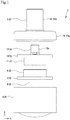
- an imaging device 1 includes a housing 2 formed of a resin molded body made of rigid resin, and an imaging component 3.
- the housing 2 includes a front housing 4 and a rear housing 5, and the imaging component 3 is accommodated inside an inner space 6 of the housing 2.
- the imaging component 3 exemplified in the exemplary embodiment includes an image pickup element 8 and an inter-substrate connecting connector 9 mounted on a first substrate 7, and an inter-substrate connecting connector 11 and a substrate-side connector 12 mounted on a second substrate 10.
- Circuit wiring of a signal processing system and various elements are mounted on the first substrate 7 and the second substrate 10, and the circuit wiring of the signal processing system and the various elements are in conductive communication with each other through the inter-substrate connecting connectors 9 and 11.
- the substrate-side connector 12 is fitted and connected to an external connection connector 13 serving as an "external device connection" provided in the rear housing 5.
- the external connection connector 13 is fitted and connected to a harness component (not shown), and the harness component is connected to an external device. As described above, an imaging signal generated by the imaging component 3 of the imaging device 1 is transmitted to the external device from the external connection connector 13 of the rear housing 5 through the harness component.
- the features of the imaging device 1 having the outlined configuration described above are the rear housing 5 and the substrate-side connector 12; accordingly, the features thereof will be described in further detail.
- the rear housing 5 includes a case portion 14 and the external connection connector 13 described above.
- the case portion 14 is made of metal, such as an aluminum alloy, and includes a polygonal tube-shaped tubular peripheral wall 14a and a wall portion 14b formed on one end side of the tubular peripheral wall 14a.
- the front housing 4 is mounted on an opening edge 14c formed on the other end side of the tubular peripheral wall 14a.
- a hole-like connection portion 14d connected to the external connection connector 13 is provided in the wall portion 14b.
- the external connection connector 13 includes a holding portion 15, a shielding member 16 serving as an "external conductor”, a dielectric 17, a pin terminal 18 serving as an "internal conductor", and a female terminal 19.
- the holding portion 15 is a molded body formed of carbon fiber reinforced resin, and is formed, by insert molding, as an integrally molded body (an insert molded body) that holds the metal case portion 14 and the metal shielding member 16.
- the carbon fiber reinforced resin of the holding portion 15 is a resin, such as a thermoplastic resin or a thermosetting resin, in which a conductive carbon fiber is dispersed and blended.
- a carbon fiber having a surface that has been treated by metal plating may be used, for example.
- the holding portion 15 will have an electromagnetic wave shielding performance; accordingly, the entire rear housing 5 will be capable of exerting an electromagnetic wave shielding effect.
- a waterproof sealing portion 20 is formed at the boundary between the holding portion 15 and the case portion 14.
- the sealing portion 20 is formed by filling a waterproof potting material.
- a case portion connection portion 15a that holds the connection portion 14d of the case portion 14 described above is formed in the holding portion 15.
- the case portion connection portion 15a is formed as a molded fixing surface by insert molding and is adhered and firmly fixed to the connection portion 14d.
- a cylindrical base portion 15b is formed in the holding portion 15.
- a shielding member connection portion 15c serving as an "external conductor connection portion” that holds the shielding member 16 is formed in the base portion 15b.
- the shielding member connection portion 15c is also formed as a molded fixing surface by insert molding and is adhered and firmly fixed to the shielding member 16.
- a cylindrical fitting portion 15d is formed on one side of the base portion 15b in the Z direction.
- a fitting chamber 15d1 to which the harness component (not shown) is fitted and connected by being inserted therein is formed inside the fitting portion 15d.
- a recess 15e is formed on the other side of the base portion 15b, and a waterproof sealing portion 15f similar to the sealing portion 20 described above is formed inside the recess 15e.
- the shielding member 16 is formed of a cylindrical metal material. A tubular portion 16a and a connector portion 16b are formed in the shielding member 16. The shielding member 16 is formed so as to have a length in the Z direction that is longer than a length of the pin terminal 18 so that an electromagnetic wave shielding effect can be exerted across the entire length of the pin terminal 18.
- the dielectric 17 is disposed inside the tubular portion 16a.
- a protrusion 16c that forms a stopper structure with respect to the shielding member connection portion 15c is formed on an outer peripheral surface of the tubular portion 16a, and joining force between the shielding member 16 and the holding portion 15 is enhanced by an increase in the area of the molded fixing surface of the shielding member connection portion 15c and the stopper structure.
- the connector portion 16b is formed so as to have a diameter that is larger than that of the tubular portion 16a, and the connector portion 16b is formed so as to be long enough to extend from the base portion 15b through the recess 15e and protrude into the inner space 6 of the rear housing 5.
- An inner space of the connector portion 16b is a fitting chamber 16d of the substrate-side connector 12.
- the female terminal 19 is disposed inside the connector portion 16b.
- the female terminal 19 is a member conductively connected to the substrate-side connector 12 and includes a pair of annular portions 19a positioned on one side and the other side in the Z direction, and curved contact spring pieces 19b that connect the annular portions 19a.
- the contact spring pieces 19b are disposed in a plural number so as to be spaced apart in the circumferential direction of the connector portion 16b and the circumferential direction of the annular portions 19a.
- the contact spring pieces 19b receiving the pressing force of the substrate-side connector 12 inserted therein become elongated such that the curvature thereof is eased, and are displaced in a direction moving the pair of annular portions 19a away from each other.
- the dielectric 17 is held by being pressed fitted inside the shielding member 16, and holds the shielding member 16 and the pin terminal 18 in an insulated state.
- a tubular fitting hole 17a is formed in the dielectric 17.
- a terminal of the harness component (not shown) is inserted into the fitting hole 17a so as to be in conductive contact with the pin terminal 18.
- An insertion and holding portion 17b of the pin terminal 18 is formed on a lower side of the fitting hole 17a.
- the pin terminal 18 is held by the insertion and holding portion 17b by being pressed-fitted therein.
- a waterproof sealing portion 17c similar to the sealing portion 20 described above is formed on the underside of the dielectric 17 so that water content does not pass through a minute gap between the pin terminal 18 and the insertion and holding portion 17b.
- the pin terminal 18 is formed of a conductive metal material and is a member that transmits an imaging signal (an electric signal) from the imaging component 3 to the harness component (not shown).
- the pin terminal 18 is held by the dielectric 17 by press-fitting a base portion 18a into the insertion and holding portion 17b of the dielectric 17.
- a round and rod-shaped harness-side connection 18b that protrudes in the fitting hole 17a of the dielectric 17 is formed on one end side of the base portion 18a, and a round and rod-shaped connector-side connection 18c that protrudes in the fitting chamber 16d of the connector portion 16b is formed on the other end side of the base portion 18a.
- the connector-side connection 18c is in conductive communication with the substrate-side connector 12 described next.
- the substrate-side connector 12 includes an outer shell wall 12a serving as a "conductive contact portion", a housing 12b, and a terminal 12c.
- the outer shell wall 12a forms an outer peripheral surface of the substrate-side connector 12 and is formed of a cylindrical sheet metal.
- An opening 12a1 is formed at an upper end of the outer shell wall 12a, and a substrate connected portion 12a2 soldered to the second substrate 10 is formed at the lower end of the outer shell wall 12a.
- the housing 12b is formed of a cylindrical resin molded body.
- the housing 12b is press-fitted inside the outer shell wall 12a and is held therewith.
- a hole-like fitting chamber 12b1 is formed in the housing 12b along the central axis.
- a portion of the fitting chamber 12b1 that corresponds to the contact pieces 12c1 of the terminal 12c described later is formed in a tapered shape and forms an inner space that allows outward displacement of the contact pieces 12c1.
- a terminal holding portion 12b2 that holds a base portion 12c2 of the terminal 12c by press-fitting is provided at a lower end of the fitting chamber 12b1.
- the terminal 12c is formed of a conductive metal material and includes the pair of contact pieces 12c1 and the base portion 12c2. The terminal 12c is held by the housing 12b through the base portion 12c2. Each of the contact pieces 12c1 is formed in a cantilevered manner extending from the base portion 12c2. Each of the contact pieces 12c1 includes an elastic arm 12c3 that extends from the base portion 12c2, and a contact portion 12c4 that has a semicircular contact surface that matches an external shape of the round and rod-shaped connector-side connection 18c of the pin terminal 18. Furthermore, substrate connected portions 12c5 that are soldered to the second substrate 10 are formed in the base portion 12c2.
- the substrate-side connector 12 having the above-described structure is mounted on the second substrate 10.
- the substrate-side connector 12 serving as a male connector and the connector portion 16b of the external connection connector 13 serving as a female connector are fitted and connected to each other.
- the outer shell wall 12a is conductively contacted to the contact spring pieces 19b of the female terminal 19.
- the second substrate 10 is conductively connected to the shielding member 16.
- the connector-side connection 18c of the pin terminal 18 is inserted between the pair of contact pieces 12c1 of the terminal 12c of the substrate-side connector 12 and is conductively contacted thereto.
- the second substrate 10 is conductively connected to the pin terminal 18.
- the imaging device 1 is conductively connected to the harness component of the external device (not shown), and the imaging signal of the imaging device 1 is transmitted to an equipment main body of the external device.
- the external connection connector 13 of the rear housing 5 includes a resin holding portion 15, and the resin holding portion 15 includes the case portion connection portion 15a that holds the metal case portion 14, and the shielding member connection portion 15c that holds the metal shielding member 16. Accordingly, the case portion 14 and the shielding member 16 that are metal materials do not have to be press-fitted to each other and, accordingly, there is no concern of displacement and falling off happening that are caused by insufficient holding force due to press-fitting the metal materials to each other. Furthermore, since the metal materials are not scratched against each other by being press-fitted to each other, there is no concern of metal burrs and metal scraps, which are the cause of short circuiting, being created.
- the heat generated by an electric component 3 can be radiated to the outside effectively with the metal case portion 14.
- the metal shielding member 16 can also exert the effect of shielding the pin terminal 18 from electromagnetic waves. Accordingly, the imaging device 1 that is suitable for high-quality and high-speed transmission of an image signal (an electric signal) from the imaging component 3 can be obtained.
- the holding portion 15 is formed as a resin molded body in which the case portion 14 and the shielding member 16 are inserted, and the case portion 14, the shielding member 16, and the holding portion 15 are configured as an integrally structured molded body manufactured through a relatively easy method.
- the integrally structured holding portion 15 can be manufactured through a relatively easy method of insert molding.
- the holding portion 15 is not a metal member but is a resin molded body, shape of the fitting portion 15d is relatively flexible. Accordingly, there is an advantage in that the fitting portion 15d can be formed according to the fitting shape of the harness component of the external device (not shown).
- the shielding member 16 includes the fitting chamber 16d that accommodates the substrate-side connector 12, and the fitting chamber 16d includes the female terminal 19 conductively contacted to the outer shell wall 12a of the substrate-side connector 12.
- the shielding member 16 is configured as a male terminal
- the connector provided in the second substrate 10 is configured as a female connector
- the area occupied by the second substrate 10 becomes large compared with a case in which the connector of the second substrate 10 is configured as a male connector, such as the substrate-side connector 12.
- the connector portion 16b of the shielding member 16 is configured as a female connector including the female terminal 19, and the substrate-side connector 12 of the second substrate 10 is configured as a male connector; accordingly, the surface occupied by the second substrate 10 can be smaller.
- the plurality of contact spring pieces 19b are disposed in the circumferential direction of the connector portion 16b. Accordingly, even if a displacement occurs when the second substrate 10 is installed in the inner space 6 of the rear housing 5, the displacement of the substrate-side connector 12 can be absorbed by the elastic deformation of the plurality of contact spring pieces 19b while in a state in which the substrate-side connector 12 is fitted in the fitting chamber 16d.
- the connector portion 16b is formed so as to have a length, from the base portion 15b, that protrudes inside the inner space 6 of the rear housing 5 through the recess 15e.
- the connector portion 16b is a "protruding end portion" of the present disclosure. Since the metal connector portion 16b protrudes in the inner space 6 of the metal case portion 14 in the above manner, while including the resin holding portion 15 in the rear housing 5, an area of the pin terminal 18 where the case portion 14 and the shielding member 16 do not overlap each other in the axial direction (the Z direction) of the case portion 14 can be eliminated; accordingly, the electromagnetic wave shielding effect can be reliably exerted on the pin terminal 18.
- the holding portion 15 is formed of a molded body made of carbon fiber reinforced resin; however, the holding portion 15 may be formed as a molded body made of thermoplastic resin or thermosetting resin in which no carbon fiber is blended.
- the outer shell wall 12a is formed in a tubular manner so that the positioning between the substrate-side connector 12 and the contact spring pieces 19b in the circumferential direction is not required; however, the outer shell wall 12a may have a divided shape so as to correspond to each of the contact spring pieces 19b.
Landscapes
- Engineering & Computer Science (AREA)
- Microelectronics & Electronic Packaging (AREA)
- Physics & Mathematics (AREA)
- Thermal Sciences (AREA)
- Multimedia (AREA)
- Signal Processing (AREA)
- Details Of Connecting Devices For Male And Female Coupling (AREA)
- Studio Devices (AREA)
- Coupling Device And Connection With Printed Circuit (AREA)
- Shielding Devices Or Components To Electric Or Magnetic Fields (AREA)
Claims (8)
- Elektronisches Bauteil für eine Abbildungsvorrichtung (1),
wobei das elektronische Bauteil folgendes aufweist:ein Gehäuse (2), das folgendes aufweist:einen Gehäuseabschnitt (14), der eine Trägerplatte (10) aufnimmt, auf der ein Verbinder (12) montiert ist, undeine externe Geräteverbindung (13), an der ein externes Gerät angebracht und mit derselben verbunden ist; undwobei die externe Geräteverbindung (13) folgendes aufweist:
einen inneren Leiter (18), der leitend mit dem externen Gerät verbunden wird, und einen rohrförmigen, metallischen, externen Leiter (16), der den inneren Leiter (18) aufnimmt,wobei der Gehäuseabschnitt (14) aus Metall hergestellt ist,wobei die externe Geräteverbindung (13) einen starren Kunststoffhalteabschnitt (15) mit einem Gehäuseabschnitts-Verbindungsabschnitt (15a), welcher den Gehäuseabschnitt (14) hält, und einen externen Leiterverbindungsabschnitt (15c), der den externen Leiter (16) hält, aufweist,dadurch gekennzeichnet, dassder Gehäuseabschnitts-Verbindungsabschnitt (15a) eine gegossene Befestigungsfläche ist, die durch Umspritzen gebildet ist und an dem Gehäuseabschnitt (14) angehaftet und fest an demselben befestigt ist,wobei der externe Leiterverbindungsabschnitt (15c) die andere gegossene Befestigungsfläche ist, die durch Umspritzen gebildet ist und an dem externen Leiter angehaftet und fest an demselben befestigt ist undwobei der Halteabschnitt (15) einteilig mit dem Gehäuseabschnitt (14) und dem externen Leiter (16) als ein Umspritzkörper ausgeführt ist. - Elektronisches Bauteil nach Anspruch 1,
wobei der Halteabschnitt (15) einen Anbringabschnitt aufweist, an dem das externe Gerät angebracht ist. - Elektronisches Bauteil nach Anspruch 1 oder 2,
wobei der externe Leiter folgendes aufweist:
eine Anbringkammer an einem Endbereich des externen Leiters auf einer Gehäuseabschnittsseite, wobei die Anbringkammer den Verbinder aufnimmt, und einen weiblichen Anschluss (19), der leitend mit dem Verbinder, der in der Anbringkammer untergebracht ist, kontaktiert ist. - Elektronisches Bauteil nach Anspruch 3,
wobei der weibliche Anschluss (19) wenigstens ein gekrümmtes Kontaktfederstück aufweist, das von einer Außenseite mit einem leitenden Kontaktabschnitt,
der auf einer äußeren Umfangsfläche des Verbinders angeordnet ist, in Pressverbindung ist. - Elektronisches Bauteil nach Anspruch 4,
wobei der weibliche Anschluss (19) eine Vielzahl der Kontaktfederstücke aufweist, wobei die Kontaktfederstücke entlang der äußeren Umfangsfläche des Verbinders angeordnet sind. - Elektronisches Bauteil nach Anspruch 1,
wobei der externe Leiter einen hervorstehenden Endabschnitt aufweist, der in einen Innenraum (6) des Gehäuseabschnitts (14) an einem Endabschnitt des äußeren Leiters auf einer Gehäuseabschnittsseite hineinragt. - Elektronisches Bauteil nach Anspruch 1,
wobei der Halteabschnitt (15) aus kohlefaserverstärktem Kunststoff gebildet ist. - Abbildungsvorrichtung (1),
welche folgendes aufweist:
das elektronische Bauteil nach Anspruch 1.
Applications Claiming Priority (1)
| Application Number | Priority Date | Filing Date | Title |
|---|---|---|---|
| JP2016238189A JP6797654B2 (ja) | 2016-12-08 | 2016-12-08 | 電子部品及び撮像装置 |
Publications (2)
| Publication Number | Publication Date |
|---|---|
| EP3333986A1 EP3333986A1 (de) | 2018-06-13 |
| EP3333986B1 true EP3333986B1 (de) | 2020-12-30 |
Family
ID=60484270
Family Applications (1)
| Application Number | Title | Priority Date | Filing Date |
|---|---|---|---|
| EP17204303.6A Active EP3333986B1 (de) | 2016-12-08 | 2017-11-29 | Elektronisches bauteil und abbildungsvorrichtung |
Country Status (4)
| Country | Link |
|---|---|
| US (1) | US10593716B2 (de) |
| EP (1) | EP3333986B1 (de) |
| JP (1) | JP6797654B2 (de) |
| CN (1) | CN108184041B (de) |
Families Citing this family (11)
| Publication number | Priority date | Publication date | Assignee | Title |
|---|---|---|---|---|
| JP6749232B2 (ja) * | 2016-12-27 | 2020-09-02 | ホシデン株式会社 | レセプタクルコネクタおよびカメラユニット |
| JP2018147844A (ja) * | 2017-03-09 | 2018-09-20 | Smk株式会社 | 電気コネクタの取付構造及び電気コネクタモジュールの製造方法 |
| JP7282449B2 (ja) * | 2019-01-31 | 2023-05-29 | ヒロセ電機株式会社 | プラグおよびレセプタクル |
| JP7189073B2 (ja) | 2019-04-22 | 2022-12-13 | 京セラ株式会社 | 電子機器、撮像装置、移動体、及び撮像装置の製造方法 |
| CN110299652A (zh) * | 2019-06-26 | 2019-10-01 | 宁波为森智能传感技术有限公司 | 一种连接器 |
| DE102020108771A1 (de) | 2020-03-30 | 2021-09-30 | Connaught Electronics Ltd. | Verfahren zur Montage einer Kamera für ein Fahrzeug, Vormontagemodul für eine Kamera, sowie Kamera |
| CN111954399B (zh) * | 2020-08-05 | 2021-05-25 | 深圳市中和智通智能科技有限公司 | 基于5g通信和区块链的智慧城市用无人驾驶汽车数据传输装置 |
| JP2024522948A (ja) * | 2021-03-22 | 2024-06-24 | タイコ エレクトロニクス アンプ コリア カンパニー リミテッド | コネクタアセンブリ |
| JP7805826B2 (ja) * | 2022-03-14 | 2026-01-26 | ホシデン株式会社 | コネクタモジュール |
| CN117638555A (zh) * | 2022-08-19 | 2024-03-01 | 上海莫仕连接器有限公司 | 电连接器 |
| JP7822289B2 (ja) * | 2022-09-27 | 2026-03-02 | ホシデン株式会社 | コネクタモジュール |
Family Cites Families (16)
| Publication number | Priority date | Publication date | Assignee | Title |
|---|---|---|---|---|
| US4453796A (en) * | 1982-06-21 | 1984-06-12 | Amp Incorporated | Coaxial connector plug |
| JP2007022364A (ja) * | 2005-07-19 | 2007-02-01 | Auto Network Gijutsu Kenkyusho:Kk | 車載カメラ |
| JP5356264B2 (ja) * | 2010-01-18 | 2013-12-04 | シャープ株式会社 | カメラモジュールおよびその製造方法、電子情報機器 |
| EP2696575B1 (de) * | 2011-04-05 | 2018-10-10 | Panasonic Intellectual Property Management Co., Ltd. | Festkörperbildaufnahmevorrichtung sowie verfahren zur herstellung der festkörperbildaufnahmevorrichtung |
| JP5725989B2 (ja) | 2011-06-14 | 2015-05-27 | 京セラ株式会社 | 撮像モジュール |
| JP6039514B2 (ja) | 2013-07-29 | 2016-12-07 | 日本航空電子工業株式会社 | 電子機器モジュール |
| US10298823B2 (en) * | 2014-02-03 | 2019-05-21 | Magna Electronics Inc. | Vehicle camera housing with tolerance compensating connector |
| US9312623B2 (en) | 2014-03-07 | 2016-04-12 | Yazaki Corporation | Connector for electronic device |
| JP2015170526A (ja) | 2014-03-07 | 2015-09-28 | 矢崎総業株式会社 | 電子機器用コネクタ |
| JP5994814B2 (ja) * | 2014-05-08 | 2016-09-21 | Smk株式会社 | コネクタ構造 |
| JP2016024862A (ja) * | 2014-07-16 | 2016-02-08 | 矢崎総業株式会社 | コネクタ及びコネクタの取付方法 |
| CN204289795U (zh) * | 2014-11-28 | 2015-04-22 | 惠州比亚迪电子有限公司 | 摄像头组件及具有其的电子设备 |
| DE102014117648A1 (de) * | 2014-12-02 | 2016-06-02 | Connaught Electronics Ltd. | Kamera für ein Kraftfahrzeug und Kraftfahrzeug |
| DE102014118175A1 (de) | 2014-12-09 | 2016-06-09 | Connaught Electronics Ltd. | Kamera für ein Kraftfahrzeug mit einer Verbindungsvorrichtung, die als oberflächenmontiertes Bauelement ausgebildet ist, sowie Kraftfahrzeug |
| CN205488716U (zh) * | 2016-03-18 | 2016-08-17 | 泰科电子(苏州)有限公司 | 同轴连接器组件、电器组件及摄像头组件 |
| CN205429250U (zh) * | 2016-03-18 | 2016-08-03 | 泰科电子(上海)有限公司 | 连接器组件和包括该连接器组件的摄像组件 |
-
2016
- 2016-12-08 JP JP2016238189A patent/JP6797654B2/ja active Active
-
2017
- 2017-11-27 CN CN201711205852.4A patent/CN108184041B/zh active Active
- 2017-11-29 EP EP17204303.6A patent/EP3333986B1/de active Active
- 2017-11-29 US US15/825,267 patent/US10593716B2/en active Active
Non-Patent Citations (1)
| Title |
|---|
| None * |
Also Published As
| Publication number | Publication date |
|---|---|
| EP3333986A1 (de) | 2018-06-13 |
| JP6797654B2 (ja) | 2020-12-09 |
| US10593716B2 (en) | 2020-03-17 |
| CN108184041B (zh) | 2021-06-01 |
| JP2018098533A (ja) | 2018-06-21 |
| CN108184041A (zh) | 2018-06-19 |
| US20180166483A1 (en) | 2018-06-14 |
Similar Documents
| Publication | Publication Date | Title |
|---|---|---|
| EP3333986B1 (de) | Elektronisches bauteil und abbildungsvorrichtung | |
| JP7361857B2 (ja) | 撮像装置用部品及び撮像装置 | |
| EP3337159A1 (de) | Elektronische komponente und bildgebungsvorrichtung | |
| US10193252B2 (en) | Electronic component and imaging device | |
| CN105100561A (zh) | 摄像装置 | |
| JP6464693B2 (ja) | モジュール用コネクタ | |
| CN108028478A (zh) | 模块用连接器 | |
| US7186037B2 (en) | Optical active connector | |
| CN112615177B (zh) | 连接器以及电子设备 | |
| US20020154871A1 (en) | Optical connector, shield casing, optical connector device | |
| KR20090105069A (ko) | 차폐형 커넥터 하우징 어셈블리 및 이를 위한 도전성탄성부재 | |
| WO2017082080A1 (ja) | モジュール用コネクタ |
Legal Events
| Date | Code | Title | Description |
|---|---|---|---|
| PUAI | Public reference made under article 153(3) epc to a published international application that has entered the european phase |
Free format text: ORIGINAL CODE: 0009012 |
|
| STAA | Information on the status of an ep patent application or granted ep patent |
Free format text: STATUS: THE APPLICATION HAS BEEN PUBLISHED |
|
| AK | Designated contracting states |
Kind code of ref document: A1 Designated state(s): AL AT BE BG CH CY CZ DE DK EE ES FI FR GB GR HR HU IE IS IT LI LT LU LV MC MK MT NL NO PL PT RO RS SE SI SK SM TR |
|
| AX | Request for extension of the european patent |
Extension state: BA ME |
|
| STAA | Information on the status of an ep patent application or granted ep patent |
Free format text: STATUS: REQUEST FOR EXAMINATION WAS MADE |
|
| 17P | Request for examination filed |
Effective date: 20181207 |
|
| RBV | Designated contracting states (corrected) |
Designated state(s): AL AT BE BG CH CY CZ DE DK EE ES FI FR GB GR HR HU IE IS IT LI LT LU LV MC MK MT NL NO PL PT RO RS SE SI SK SM TR |
|
| STAA | Information on the status of an ep patent application or granted ep patent |
Free format text: STATUS: EXAMINATION IS IN PROGRESS |
|
| 17Q | First examination report despatched |
Effective date: 20191023 |
|
| GRAP | Despatch of communication of intention to grant a patent |
Free format text: ORIGINAL CODE: EPIDOSNIGR1 |
|
| STAA | Information on the status of an ep patent application or granted ep patent |
Free format text: STATUS: GRANT OF PATENT IS INTENDED |
|
| RIC1 | Information provided on ipc code assigned before grant |
Ipc: H01R 13/6581 20110101ALI20200904BHEP Ipc: H01R 13/504 20060101AFI20200904BHEP Ipc: H01R 24/52 20110101ALN20200904BHEP Ipc: H01R 13/405 20060101ALN20200904BHEP |
|
| INTG | Intention to grant announced |
Effective date: 20200925 |
|
| GRAS | Grant fee paid |
Free format text: ORIGINAL CODE: EPIDOSNIGR3 |
|
| GRAA | (expected) grant |
Free format text: ORIGINAL CODE: 0009210 |
|
| STAA | Information on the status of an ep patent application or granted ep patent |
Free format text: STATUS: THE PATENT HAS BEEN GRANTED |
|
| AK | Designated contracting states |
Kind code of ref document: B1 Designated state(s): AL AT BE BG CH CY CZ DE DK EE ES FI FR GB GR HR HU IE IS IT LI LT LU LV MC MK MT NL NO PL PT RO RS SE SI SK SM TR |
|
| REG | Reference to a national code |
Ref country code: GB Ref legal event code: FG4D |
|
| REG | Reference to a national code |
Ref country code: DE Ref legal event code: R096 Ref document number: 602017030390 Country of ref document: DE |
|
| REG | Reference to a national code |
Ref country code: AT Ref legal event code: REF Ref document number: 1350868 Country of ref document: AT Kind code of ref document: T Effective date: 20210115 |
|
| REG | Reference to a national code |
Ref country code: IE Ref legal event code: FG4D |
|
| PG25 | Lapsed in a contracting state [announced via postgrant information from national office to epo] |
Ref country code: GR Free format text: LAPSE BECAUSE OF FAILURE TO SUBMIT A TRANSLATION OF THE DESCRIPTION OR TO PAY THE FEE WITHIN THE PRESCRIBED TIME-LIMIT Effective date: 20210331 Ref country code: FI Free format text: LAPSE BECAUSE OF FAILURE TO SUBMIT A TRANSLATION OF THE DESCRIPTION OR TO PAY THE FEE WITHIN THE PRESCRIBED TIME-LIMIT Effective date: 20201230 Ref country code: NO Free format text: LAPSE BECAUSE OF FAILURE TO SUBMIT A TRANSLATION OF THE DESCRIPTION OR TO PAY THE FEE WITHIN THE PRESCRIBED TIME-LIMIT Effective date: 20210330 Ref country code: RS Free format text: LAPSE BECAUSE OF FAILURE TO SUBMIT A TRANSLATION OF THE DESCRIPTION OR TO PAY THE FEE WITHIN THE PRESCRIBED TIME-LIMIT Effective date: 20201230 |
|
| REG | Reference to a national code |
Ref country code: AT Ref legal event code: MK05 Ref document number: 1350868 Country of ref document: AT Kind code of ref document: T Effective date: 20201230 |
|
| PG25 | Lapsed in a contracting state [announced via postgrant information from national office to epo] |
Ref country code: SE Free format text: LAPSE BECAUSE OF FAILURE TO SUBMIT A TRANSLATION OF THE DESCRIPTION OR TO PAY THE FEE WITHIN THE PRESCRIBED TIME-LIMIT Effective date: 20201230 Ref country code: BG Free format text: LAPSE BECAUSE OF FAILURE TO SUBMIT A TRANSLATION OF THE DESCRIPTION OR TO PAY THE FEE WITHIN THE PRESCRIBED TIME-LIMIT Effective date: 20210330 Ref country code: LV Free format text: LAPSE BECAUSE OF FAILURE TO SUBMIT A TRANSLATION OF THE DESCRIPTION OR TO PAY THE FEE WITHIN THE PRESCRIBED TIME-LIMIT Effective date: 20201230 |
|
| REG | Reference to a national code |
Ref country code: NL Ref legal event code: MP Effective date: 20201230 |
|
| PG25 | Lapsed in a contracting state [announced via postgrant information from national office to epo] |
Ref country code: HR Free format text: LAPSE BECAUSE OF FAILURE TO SUBMIT A TRANSLATION OF THE DESCRIPTION OR TO PAY THE FEE WITHIN THE PRESCRIBED TIME-LIMIT Effective date: 20201230 |
|
| REG | Reference to a national code |
Ref country code: LT Ref legal event code: MG9D |
|
| PG25 | Lapsed in a contracting state [announced via postgrant information from national office to epo] |
Ref country code: LT Free format text: LAPSE BECAUSE OF FAILURE TO SUBMIT A TRANSLATION OF THE DESCRIPTION OR TO PAY THE FEE WITHIN THE PRESCRIBED TIME-LIMIT Effective date: 20201230 Ref country code: EE Free format text: LAPSE BECAUSE OF FAILURE TO SUBMIT A TRANSLATION OF THE DESCRIPTION OR TO PAY THE FEE WITHIN THE PRESCRIBED TIME-LIMIT Effective date: 20201230 Ref country code: CZ Free format text: LAPSE BECAUSE OF FAILURE TO SUBMIT A TRANSLATION OF THE DESCRIPTION OR TO PAY THE FEE WITHIN THE PRESCRIBED TIME-LIMIT Effective date: 20201230 Ref country code: PT Free format text: LAPSE BECAUSE OF FAILURE TO SUBMIT A TRANSLATION OF THE DESCRIPTION OR TO PAY THE FEE WITHIN THE PRESCRIBED TIME-LIMIT Effective date: 20210430 Ref country code: SK Free format text: LAPSE BECAUSE OF FAILURE TO SUBMIT A TRANSLATION OF THE DESCRIPTION OR TO PAY THE FEE WITHIN THE PRESCRIBED TIME-LIMIT Effective date: 20201230 Ref country code: RO Free format text: LAPSE BECAUSE OF FAILURE TO SUBMIT A TRANSLATION OF THE DESCRIPTION OR TO PAY THE FEE WITHIN THE PRESCRIBED TIME-LIMIT Effective date: 20201230 |
|
| PG25 | Lapsed in a contracting state [announced via postgrant information from national office to epo] |
Ref country code: PL Free format text: LAPSE BECAUSE OF FAILURE TO SUBMIT A TRANSLATION OF THE DESCRIPTION OR TO PAY THE FEE WITHIN THE PRESCRIBED TIME-LIMIT Effective date: 20201230 Ref country code: AT Free format text: LAPSE BECAUSE OF FAILURE TO SUBMIT A TRANSLATION OF THE DESCRIPTION OR TO PAY THE FEE WITHIN THE PRESCRIBED TIME-LIMIT Effective date: 20201230 |
|
| PG25 | Lapsed in a contracting state [announced via postgrant information from national office to epo] |
Ref country code: IS Free format text: LAPSE BECAUSE OF FAILURE TO SUBMIT A TRANSLATION OF THE DESCRIPTION OR TO PAY THE FEE WITHIN THE PRESCRIBED TIME-LIMIT Effective date: 20210430 |
|
| REG | Reference to a national code |
Ref country code: DE Ref legal event code: R097 Ref document number: 602017030390 Country of ref document: DE |
|
| PG25 | Lapsed in a contracting state [announced via postgrant information from national office to epo] |
Ref country code: AL Free format text: LAPSE BECAUSE OF FAILURE TO SUBMIT A TRANSLATION OF THE DESCRIPTION OR TO PAY THE FEE WITHIN THE PRESCRIBED TIME-LIMIT Effective date: 20201230 Ref country code: IT Free format text: LAPSE BECAUSE OF FAILURE TO SUBMIT A TRANSLATION OF THE DESCRIPTION OR TO PAY THE FEE WITHIN THE PRESCRIBED TIME-LIMIT Effective date: 20201230 |
|
| PLBE | No opposition filed within time limit |
Free format text: ORIGINAL CODE: 0009261 |
|
| STAA | Information on the status of an ep patent application or granted ep patent |
Free format text: STATUS: NO OPPOSITION FILED WITHIN TIME LIMIT |
|
| PG25 | Lapsed in a contracting state [announced via postgrant information from national office to epo] |
Ref country code: DK Free format text: LAPSE BECAUSE OF FAILURE TO SUBMIT A TRANSLATION OF THE DESCRIPTION OR TO PAY THE FEE WITHIN THE PRESCRIBED TIME-LIMIT Effective date: 20201230 |
|
| 26N | No opposition filed |
Effective date: 20211001 |
|
| PG25 | Lapsed in a contracting state [announced via postgrant information from national office to epo] |
Ref country code: ES Free format text: LAPSE BECAUSE OF FAILURE TO SUBMIT A TRANSLATION OF THE DESCRIPTION OR TO PAY THE FEE WITHIN THE PRESCRIBED TIME-LIMIT Effective date: 20201230 |
|
| PG25 | Lapsed in a contracting state [announced via postgrant information from national office to epo] |
Ref country code: SI Free format text: LAPSE BECAUSE OF FAILURE TO SUBMIT A TRANSLATION OF THE DESCRIPTION OR TO PAY THE FEE WITHIN THE PRESCRIBED TIME-LIMIT Effective date: 20201230 |
|
| PG25 | Lapsed in a contracting state [announced via postgrant information from national office to epo] |
Ref country code: IS Free format text: LAPSE BECAUSE OF FAILURE TO SUBMIT A TRANSLATION OF THE DESCRIPTION OR TO PAY THE FEE WITHIN THE PRESCRIBED TIME-LIMIT Effective date: 20210430 |
|
| PG25 | Lapsed in a contracting state [announced via postgrant information from national office to epo] |
Ref country code: MC Free format text: LAPSE BECAUSE OF FAILURE TO SUBMIT A TRANSLATION OF THE DESCRIPTION OR TO PAY THE FEE WITHIN THE PRESCRIBED TIME-LIMIT Effective date: 20201230 |
|
| REG | Reference to a national code |
Ref country code: CH Ref legal event code: PL |
|
| GBPC | Gb: european patent ceased through non-payment of renewal fee |
Effective date: 20211129 |
|
| PG25 | Lapsed in a contracting state [announced via postgrant information from national office to epo] |
Ref country code: LU Free format text: LAPSE BECAUSE OF NON-PAYMENT OF DUE FEES Effective date: 20211129 Ref country code: BE Free format text: LAPSE BECAUSE OF NON-PAYMENT OF DUE FEES Effective date: 20211130 |
|
| REG | Reference to a national code |
Ref country code: BE Ref legal event code: MM Effective date: 20211130 |
|
| PG25 | Lapsed in a contracting state [announced via postgrant information from national office to epo] |
Ref country code: LI Free format text: LAPSE BECAUSE OF NON-PAYMENT OF DUE FEES Effective date: 20211130 Ref country code: CH Free format text: LAPSE BECAUSE OF NON-PAYMENT OF DUE FEES Effective date: 20211130 |
|
| PG25 | Lapsed in a contracting state [announced via postgrant information from national office to epo] |
Ref country code: IE Free format text: LAPSE BECAUSE OF NON-PAYMENT OF DUE FEES Effective date: 20211129 Ref country code: GB Free format text: LAPSE BECAUSE OF NON-PAYMENT OF DUE FEES Effective date: 20211129 |
|
| PG25 | Lapsed in a contracting state [announced via postgrant information from national office to epo] |
Ref country code: FR Free format text: LAPSE BECAUSE OF NON-PAYMENT OF DUE FEES Effective date: 20211130 |
|
| PG25 | Lapsed in a contracting state [announced via postgrant information from national office to epo] |
Ref country code: HU Free format text: LAPSE BECAUSE OF FAILURE TO SUBMIT A TRANSLATION OF THE DESCRIPTION OR TO PAY THE FEE WITHIN THE PRESCRIBED TIME-LIMIT; INVALID AB INITIO Effective date: 20171129 |
|
| PG25 | Lapsed in a contracting state [announced via postgrant information from national office to epo] |
Ref country code: NL Free format text: LAPSE BECAUSE OF NON-PAYMENT OF DUE FEES Effective date: 20201230 Ref country code: CY Free format text: LAPSE BECAUSE OF FAILURE TO SUBMIT A TRANSLATION OF THE DESCRIPTION OR TO PAY THE FEE WITHIN THE PRESCRIBED TIME-LIMIT Effective date: 20201230 |
|
| PG25 | Lapsed in a contracting state [announced via postgrant information from national office to epo] |
Ref country code: SM Free format text: LAPSE BECAUSE OF FAILURE TO SUBMIT A TRANSLATION OF THE DESCRIPTION OR TO PAY THE FEE WITHIN THE PRESCRIBED TIME-LIMIT Effective date: 20201230 |
|
| PG25 | Lapsed in a contracting state [announced via postgrant information from national office to epo] |
Ref country code: MK Free format text: LAPSE BECAUSE OF FAILURE TO SUBMIT A TRANSLATION OF THE DESCRIPTION OR TO PAY THE FEE WITHIN THE PRESCRIBED TIME-LIMIT Effective date: 20201230 |
|
| PG25 | Lapsed in a contracting state [announced via postgrant information from national office to epo] |
Ref country code: MT Free format text: LAPSE BECAUSE OF FAILURE TO SUBMIT A TRANSLATION OF THE DESCRIPTION OR TO PAY THE FEE WITHIN THE PRESCRIBED TIME-LIMIT Effective date: 20201230 |
|
| PG25 | Lapsed in a contracting state [announced via postgrant information from national office to epo] |
Ref country code: TR Free format text: LAPSE BECAUSE OF FAILURE TO SUBMIT A TRANSLATION OF THE DESCRIPTION OR TO PAY THE FEE WITHIN THE PRESCRIBED TIME-LIMIT Effective date: 20201230 |
|
| PGFP | Annual fee paid to national office [announced via postgrant information from national office to epo] |
Ref country code: DE Payment date: 20251119 Year of fee payment: 9 |