EP3334151B1 - Verfahren zur ansteuerung eines bildsensors - Google Patents
Verfahren zur ansteuerung eines bildsensors Download PDFInfo
- Publication number
- EP3334151B1 EP3334151B1 EP16832502.5A EP16832502A EP3334151B1 EP 3334151 B1 EP3334151 B1 EP 3334151B1 EP 16832502 A EP16832502 A EP 16832502A EP 3334151 B1 EP3334151 B1 EP 3334151B1
- Authority
- EP
- European Patent Office
- Prior art keywords
- exposure
- gate
- imaging device
- state imaging
- solid
- Prior art date
- Legal status (The legal status is an assumption and is not a legal conclusion. Google has not performed a legal analysis and makes no representation as to the accuracy of the status listed.)
- Active
Links
Images


Classifications
-
- G—PHYSICS
- G01—MEASURING; TESTING
- G01S—RADIO DIRECTION-FINDING; RADIO NAVIGATION; DETERMINING DISTANCE OR VELOCITY BY USE OF RADIO WAVES; LOCATING OR PRESENCE-DETECTING BY USE OF THE REFLECTION OR RERADIATION OF RADIO WAVES; ANALOGOUS ARRANGEMENTS USING OTHER WAVES
- G01S7/00—Details of systems according to groups G01S13/00, G01S15/00, G01S17/00
- G01S7/48—Details of systems according to groups G01S13/00, G01S15/00, G01S17/00 of systems according to group G01S17/00
- G01S7/483—Details of pulse systems
- G01S7/486—Receivers
- G01S7/4868—Controlling received signal intensity or exposure of sensor
-
- G—PHYSICS
- G01—MEASURING; TESTING
- G01S—RADIO DIRECTION-FINDING; RADIO NAVIGATION; DETERMINING DISTANCE OR VELOCITY BY USE OF RADIO WAVES; LOCATING OR PRESENCE-DETECTING BY USE OF THE REFLECTION OR RERADIATION OF RADIO WAVES; ANALOGOUS ARRANGEMENTS USING OTHER WAVES
- G01S17/00—Systems using the reflection or reradiation of electromagnetic waves other than radio waves, e.g. lidar systems
- G01S17/02—Systems using the reflection of electromagnetic waves other than radio waves
- G01S17/06—Systems determining position data of a target
- G01S17/08—Systems determining position data of a target for measuring distance only
- G01S17/10—Systems determining position data of a target for measuring distance only using transmission of interrupted, pulse-modulated waves
-
- G—PHYSICS
- G01—MEASURING; TESTING
- G01S—RADIO DIRECTION-FINDING; RADIO NAVIGATION; DETERMINING DISTANCE OR VELOCITY BY USE OF RADIO WAVES; LOCATING OR PRESENCE-DETECTING BY USE OF THE REFLECTION OR RERADIATION OF RADIO WAVES; ANALOGOUS ARRANGEMENTS USING OTHER WAVES
- G01S17/00—Systems using the reflection or reradiation of electromagnetic waves other than radio waves, e.g. lidar systems
- G01S17/88—Lidar systems specially adapted for specific applications
- G01S17/89—Lidar systems specially adapted for specific applications for mapping or imaging
- G01S17/894—Three-dimensional [3D] imaging with simultaneous measurement of time-of-flight at a two-dimensional [2D] array of receiver pixels, e.g. time-of-flight cameras or flash lidar
-
- G—PHYSICS
- G01—MEASURING; TESTING
- G01S—RADIO DIRECTION-FINDING; RADIO NAVIGATION; DETERMINING DISTANCE OR VELOCITY BY USE OF RADIO WAVES; LOCATING OR PRESENCE-DETECTING BY USE OF THE REFLECTION OR RERADIATION OF RADIO WAVES; ANALOGOUS ARRANGEMENTS USING OTHER WAVES
- G01S7/00—Details of systems according to groups G01S13/00, G01S15/00, G01S17/00
- G01S7/48—Details of systems according to groups G01S13/00, G01S15/00, G01S17/00 of systems according to group G01S17/00
- G01S7/483—Details of pulse systems
- G01S7/486—Receivers
- G01S7/4861—Circuits for detection, sampling, integration or read-out
- G01S7/4863—Detector arrays, e.g. charge-transfer gates
-
- G—PHYSICS
- G01—MEASURING; TESTING
- G01S—RADIO DIRECTION-FINDING; RADIO NAVIGATION; DETERMINING DISTANCE OR VELOCITY BY USE OF RADIO WAVES; LOCATING OR PRESENCE-DETECTING BY USE OF THE REFLECTION OR RERADIATION OF RADIO WAVES; ANALOGOUS ARRANGEMENTS USING OTHER WAVES
- G01S7/00—Details of systems according to groups G01S13/00, G01S15/00, G01S17/00
- G01S7/48—Details of systems according to groups G01S13/00, G01S15/00, G01S17/00 of systems according to group G01S17/00
- G01S7/483—Details of pulse systems
- G01S7/486—Receivers
- G01S7/4865—Time delay measurement, e.g. time-of-flight measurement, time of arrival measurement or determining the exact position of a peak
-
- H—ELECTRICITY
- H04—ELECTRIC COMMUNICATION TECHNIQUE
- H04N—PICTORIAL COMMUNICATION, e.g. TELEVISION
- H04N23/00—Cameras or camera modules comprising electronic image sensors; Control thereof
- H04N23/70—Circuitry for compensating brightness variation in the scene
- H04N23/71—Circuitry for evaluating the brightness variation
-
- H—ELECTRICITY
- H04—ELECTRIC COMMUNICATION TECHNIQUE
- H04N—PICTORIAL COMMUNICATION, e.g. TELEVISION
- H04N25/00—Circuitry of solid-state image sensors [SSIS]; Control thereof
- H04N25/50—Control of the SSIS exposure
- H04N25/53—Control of the integration time
-
- H—ELECTRICITY
- H04—ELECTRIC COMMUNICATION TECHNIQUE
- H04N—PICTORIAL COMMUNICATION, e.g. TELEVISION
- H04N25/00—Circuitry of solid-state image sensors [SSIS]; Control thereof
- H04N25/70—SSIS architectures; Circuits associated therewith
- H04N25/76—Addressed sensors, e.g. MOS or CMOS sensors
-
- H—ELECTRICITY
- H10—SEMICONDUCTOR DEVICES; ELECTRIC SOLID-STATE DEVICES NOT OTHERWISE PROVIDED FOR
- H10F—INORGANIC SEMICONDUCTOR DEVICES SENSITIVE TO INFRARED RADIATION, LIGHT, ELECTROMAGNETIC RADIATION OF SHORTER WAVELENGTH OR CORPUSCULAR RADIATION
- H10F39/00—Integrated devices, or assemblies of multiple devices, comprising at least one element covered by group H10F30/00, e.g. radiation detectors comprising photodiode arrays
- H10F39/10—Integrated devices
- H10F39/12—Image sensors
- H10F39/15—Charge-coupled device [CCD] image sensors
- H10F39/151—Geometry or disposition of pixel elements, address lines or gate electrodes
- H10F39/1515—Optical shielding
-
- H—ELECTRICITY
- H10—SEMICONDUCTOR DEVICES; ELECTRIC SOLID-STATE DEVICES NOT OTHERWISE PROVIDED FOR
- H10F—INORGANIC SEMICONDUCTOR DEVICES SENSITIVE TO INFRARED RADIATION, LIGHT, ELECTROMAGNETIC RADIATION OF SHORTER WAVELENGTH OR CORPUSCULAR RADIATION
- H10F39/00—Integrated devices, or assemblies of multiple devices, comprising at least one element covered by group H10F30/00, e.g. radiation detectors comprising photodiode arrays
- H10F39/10—Integrated devices
- H10F39/12—Image sensors
- H10F39/15—Charge-coupled device [CCD] image sensors
- H10F39/153—Two-dimensional or three-dimensional array CCD image sensors
- H10F39/1538—Time-delay and integration
Definitions
- the present invention relates to methods for driving solid-state imaging devices to be used in imaging for distance measurement.
- TOF time of flight
- Patent Literature (PTL) 1 discloses a distance image sensor in which two different signal storage units store signals obtained by transfer of charge with different phases in synchronization with intermittent behavior of light from a light source, the distance to an object is determined using the distribution ratio of the stored signals, and furthermore, a third signal storage unit stores signals of background light only, and thus background light removal is performed to eliminate the impact of the background light
- Patent Literature (PTL) 2 discloses an optical distance measuring device having a pulsed radiation source that is implemented to transmit, in a temporally contiguous radiation pulse period, a radiation pulse having a pulse duration tp that is shorter than the radiation pulse period, and to transmit no radiation pulse in a temporally contiguous dark period.
- the optical distance measuring device includes a detector for detecting different amounts of radiation in two overlapping detection periods during the radiation pulse period to capture reflections of the radiation pulse at an object surface and a background radiation and/or in two overlapping detection periods during the dark period to capture background radiation.
- the optical distance measuring device further includes an evaluator determining a signal depending on a distance of the optical distance measuring device to an object based on the detected amount of radiation.
- the present invention provides a method for optical distance measurement and for multiple sampling.
- exposure periods T1 to T3 are set to have the same length as pulse width Tp where T1 is a first exposure period starting from time of a rising edge of irradiating light having pulse width Tp, T2 is a second exposure period starting from time of a falling edge of the irradiating light, and T3 is a third exposure period in which exposure is performed in a state where the irradiating light is OFF.
- the present invention has an object to provide a method for driving a solid-state imaging device which is small, has high distance measurement accuracy, and obtains a distance measurement signal that covers a wide distance measurement range.
- a small solid-state imaging device can obtain a distance measurement signal that covers a wide distance measurement range with high distance measurement accuracy.
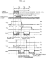
- FIG. 15A is a schematic configuration view of a conventional distance measurement pixel which obtains distance measurement information using three unit pixels.
- FIG. 15B is a timing chart for describing distance measurement driving of a conventional distance measurement device.
- FIG. 16 illustrates transitions of a pixel potential distribution at the time of distance measurement driving of the conventional distance measurement device.
- FIG. 15A structural elements of three unit pixels 70A, 70B, and 70C are illustrated, and three unit pixels 70A, 70B, and 70C form one distance measurement pixel 70.
- Unit pixel 70A includes one photoelectric conversion element 50A, read gate TG0, charge accumulation gate SG0, output gate OG0, and exposure reset gate PRS0.
- Unit pixel 70B includes one photoelectric conversion element 50B, a read gate TG1, charge accumulation gate SG1, output gate OG1, and exposure reset gate PRS1.
- Unit pixel 70C includes one photoelectric conversion element 50C, read gate TG2, charge accumulation gate SG2, output gate OG2, and exposure reset gate PRS2.
- distance measurement pixel 70 includes: floating diffusion (FD) 61 which is shared by three unit pixels 70A, 70B, and 70C; amplification transistor 63; reset transistor 64; and selection transistor 65.
- FD floating diffusion
- distance measurement pixel 70 having the abovementioned configuration, as illustrated in FIG. 15B , at the time of exposure of each photoelectric conversion element, the operation of starting the signal reading from the photoelectric conversion element to the charge accumulation gate and the operation of stopping the signal discharge from the photoelectric conversion element to drain VPRD are performed at the same time. Furthermore, the operation of stopping the signal reading from the photoelectric conversion element to the charge accumulation gate and the operation of starting the signal discharge from the photoelectric conversion element to drain VPRD are performed at the same time. Next, distance measurement driving of the conventional distance measurement device will be described.
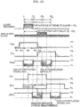
- read gate TG0 of unit pixel 70A (S0 exposure pixel) is OFF, exposure reset gate PRS0 is ON, and signal charge of photoelectric conversion element 50A is discharged to drain VPRD (P1 in FIG. 16 : discharge).
- read gate TG0 is switched OFF again (VH to VL), and exposure reset gate PRS0 is switched ON (VL to VH); thus, the charge of photoelectric conversion element 50A is discharged to drain VPRD, resulting in completion of S0 exposure sequence at unit pixel 70A.
- read gate TG1 is switched ON (VL to VH), and exposure reset gate PRS1 is switched OFF (VH to VL); thus, the signal charge of photoelectric conversion element 50B is transferred to charge accumulation gate SG1 and accumulated therein.
- read gate TG1 is switched OFF again (VH to VL), and exposure reset gate PRS1 is switched ON (VL to VH); thus, the charge of photoelectric conversion element 50B is discharged to drain VPRD, resulting in completion of S1 exposure sequence at unit pixel 70B.
- unit pixel 70C (BG exposure pixel)
- read gate TG2 is OFF
- exposure reset gate PRS2 is ON
- signal charge of photoelectric conversion element 50C is discharged to drain VPRD.
- read gate TG2 is switched ON (VL to VH), and exposure reset gate PRS2 is switched OFF (VH to VL); thus, the signal charge of photoelectric conversion element 50C is transferred to charge accumulation gate SG2 and accumulated therein.
- read gate TG2 is switched OFF again (VH to VL), and exposure reset gate PRS2 is switched ON (VL to VH); thus, the charge of photoelectric conversion element 50C is discharged to drain VPRD, resulting in completion of BG exposure sequence at unit pixel 70C.
- S0 exposure sequence, S1 exposure sequence, and BG exposure sequence are repeated several hundred to several hundred thousand times, the amount of accumulated signals in a charge accumulation transistor having charge accumulation gate SG is increased, and thereafter output gate OG is switched ON so that the charge accumulated in the charge accumulation transistor is transferred, and charge accumulation gate SG is switched OFF and output gate OG is switched OFF in sequence so that all of the accumulated charge is transferred and output to FD 61.
- three unit pixels form one distance measurement pixel, and distance measurement calculation is performed through one light emission and three exposure processes using three unit pixels.
- Equation 1 to Equation 4 distance L to a subject can be calculated on a per-distance-measurement-pixel basis according to Equation 1 to Equation 4 below.
- S0' represents the signal charge accumulated in charge accumulation gate SG0 in the S0 exposure sequence at unit pixel 70A
- S1' represents the signal charge accumulated in charge accumulation gate SG1 in the S1 exposure sequence at unit pixel 70B
- BG2 represents the signal charge accumulated in charge accumulation gate SG2 in the BG exposure sequence at unit pixel 70C.
- the conventional distance measurement device described above has the following problems.
- FIG. 17 illustrates the arrangement of a conventional distance measurement pixel which obtains distance measurement information using three unit pixels.
- Recent years have seen a sharp rise in the demand for small, high-resolution (at least QVGA) TOF sensors for a machine vision application, a gesture input application, etc., in the field of mobile, robot, and vehicle-mounted devices, for example. Accordingly, the realization of small, high-resolution TOF sensors capable of measuring a distance using miniaturized distance measurement pixels is awaited.
- each unit pixel performs one accumulation, and therefore three unit pixels are needed to obtain three signals (S0', S1', BG) required for distance measurement, causing an increase in the size of the distance measurement pixel.
- the optical size of the TOF sensor needs to be increased, as illustrated in FIG. 17 .
- Equation 4 As illustrated in the circuit diagram of the distance measurement pixel in FIG. 15A and the distance measurement drive timing in FIG. 15B , when S0 and S1 to be used in Equation 4 for calculating distance L are derived from Equation 1, the BG component is subtracted using BG2 accumulated in the charge accumulation transistor of unit pixel 70C.
- respective background light components actually contained in S0' and S1' are signals BG0 and BG1 obtained by the exposure of unit pixel 70A and 70B, which are different from unit pixel 70C.
- FIG. 18 is a timing chart for describing misaligned drive timing in distance measurement driving of a conventional distance measurement device.
- the timing at which read gate TG is switched ON and the timing at which exposure reset gate PRS is switched OFF are the same, and the timing at which the read gate is switched OFF and the timing at which exposure reset gate PRS is switched ON are the same. Since these pulses are applied from the periphery of a pixel region into the pixel region, the roundness of the pulse waveform, delayed timing, etc., cause a temporal misalignment of the ON/OFF timing for read gate TG with that of exposure reset gate PRS, as illustrated in FIG.
- the present invention has been conceived in order to such problems, and aims to provide a solid-state imaging device which is small, has high distance measurement accuracy, and obtains a distance measurement signal that covers a wide distance measurement range, and provide a method for driving the solid-state imaging device.
- FIG. 1 is a function block diagram illustrating an example of an outline configuration of solid-state imaging device 1000 according to Embodiment 1. As illustrated in this figure, solid-state imaging device 1000 includes imager 100, light source driver 200, drive controller 300, optical lens 400, and light source unit 500.
- Solid-state imaging device 1000 functions as a distance measurement imaging device which measures the distance to object 600, by emitting infrared light or the like from light source unit 500 toward object 600 and receiving, by imager 100, light reflected from object 600.
- Light source driver 200 generates a light emission signal instructing light irradiation to object 600.
- light source unit 500 irradiates object 600 with light using a light emission current generated by light source driver 200.
- Imager 100 includes an imaging region in which unit pixels including photoelectric conversion elements are two-dimensionally arranged, and performs exposure on a region including object 600 plural times according to timing indicated by the exposure signal generated by drive controller 300, and generates a distance measurement signal corresponding to the total amount of exposure performed plural times.
- the drive controller generates an exposure signal instructing exposure to light reflected from object 600, and calculates the distance to object 600 on the basis of the distance measurement signal received from imager 100.
- light source unit 500 emits near infrared light toward object 600 under background light, for example.
- the light reflected from object 600 enters imager 100 through optical lens 400.
- the reflected light incident on imager 100 forms an image, and the formed image is converted into an electrical signal.
- the operations of light source unit 500 and imager 100 are controlled by drive controller 300.
- the output of imager 100 is converted into a distance image, and also into a visible image depending on the usage, by drive controller 300.
- imager 100 is a solid-state imaging element such as what is called a complementary metal-oxide-semiconductor (CMOS) image sensor.
- CMOS complementary metal-oxide-semiconductor
- the solid-state imaging device according to the present invention is not required to include light source unit 500 and light source driver 200 which actively emit light toward object 600 unlike solid-state imaging device 1000 according to the present embodiment.
- the solid-state imaging device according to the present invention may obtain luminance information, etc., of object 600 by receiving external irradiating light (including natural light) reflected from object 600.
- FIG. 2 illustrates a circuit configuration of a distance measurement pixel of the solid-state imaging device according to Embodiment 1. This figure illustrates a circuit configuration of a distance measurement pixel two-dimensionally arranged in the imaging region of imager 100 according to the present embodiment. As illustrated in FIG.
- distance measurement pixel 10 includes: two unit pixels 10A and 10B which receive reflected light, photoelectrically convert the reflected light into signal charge, and accumulate and output the signal charge; one floating diffusion layer (FD) 21 which converts the signal charge into a voltage; reset (RST) transistor 24 which discharges the signal charge of FD 21 to a reset drain (VRD); amplification transistor 23 which is connected to a VDD power supply and amplifies a signal from FD 21; and selection (SEL) transistor 25 which outputs and controls a signal from amplification transistor 23 in accordance with an exteriorly obtained selection signal.
- FD floating diffusion layer
- RST reset
- VRD reset drain
- amplification transistor 23 which is connected to a VDD power supply and amplifies a signal from FD 21
- selection (SEL) transistor 25 which outputs and controls a signal from amplification transistor 23 in accordance with an exteriorly obtained selection signal.
- Each of two unit pixels 10A and 10B includes: one light receiver which receives the reflected light and photoelectrically converts the received light; one charge reset transistor which discharges, to a charge discharger, a signal obtained from the light receiver; two read transistors which read the signal from the light receiver; two charge accumulation transistors which accumulate the signal read by the two read transistors; and one or two output transistors which output the signal accumulated in the charge accumulation transistors.
- Each of the above-mentioned transistors has a structure in which a gate insulating film and a gate electrode are formed in this order above a semiconductor substrate, and can switch between a conducting state and a non-conducting state between a source and a drain using a drive pulse signal supplied from the gate electrode.
- each of the transistors or the gate electrode thereof may be referred to simply as a gate.
- unit pixel 10A includes one photoelectric conversion element 1A, read gates TG0 and TG2, charge accumulation gates SG0 and SG2, output gates OG0 and OG2, and charge reset gates PRS0.
- Unit pixel 10B includes one photoelectric conversion element 1B, read gates TG1 and TG3, charge accumulation gates SG1 and SG3, output gates OG1 and OG3, and charge reset gates PRS1.
- the number of read transistors, charge accumulation transistors, and output transistors included in one unit pixel is twice as large as that in the related art.
- These transistors can be formed within an element isolation region between the photoelectric conversion elements with the recent, finer CMOS process technology as long as the pixel size is in the range of 2 ⁇ m to 50 ⁇ m, which is typical for the TOF sensors, and thus it is possible to provide a sufficient area for the photoelectric conversion elements.
- FIG. 3 illustrates a cross-sectional structure of the unit pixel according to Embodiment 1. Specifically, the cross-sectional structure of a charge transfer path to which read gate TG2 of unit pixel 10A belongs is depicted in FIG. 3 .
- photoelectric conversion element 1A PDO
- RG2 read transistor
- PRS0 charge reset transistor
- the drain (VPRD) adjacent to the charge reset transistor (PRS0) is formed in a n+-type region.
- the drain (VPRD) discharges the signal charge from photoelectric conversion element 1A (PD0) via the charge reset transistor (PRS0), and thus is connected to a VH power supply.
- the signal charge accumulated in the charge accumulation transistor (SG2) is transferred to FD 21 via the output transistor (OG2) on the same principle as a charge-coupled device, and thus the charge accumulation transistor (SG2) and the output transistor (OG2) adjacent to the read transistor (TG2) are formed with an n-type buried channel.
- Light-shielding film 30 made from a metal or a metallic compound including tungsten (W), aluminum (Al), and copper (Cu) is formed at least on the charge accumulation transistor (SG2) so as not to allow the direct entry of the reflected light, the background light, and the like at the time of signal accumulation.
- Microlens 40 is formed above light-shielding film 30 via waveguide path LP, allowing the reflected light directed to unit pixel 10A to be efficiently condensed onto photoelectric conversion element 1A (PD0).
- light-shielding film 30 may be formed above the charge reset transistor (PRS0). In the present embodiment, however, since the charge reset transistor needs to be turned ON and OFF at very high speed, light-shielding film 30 is preferably unformed, with priority placed on the property of reducing parasitic capacitance.
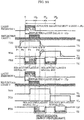
- FIG. 4A is a distance measurement drive timing chart for short-distance object measurement of the solid-state imaging device according to Embodiment 1.
- FIG. 4B is a distance measurement drive timing chart for medium-distance object measurement of the solid-state imaging device according to Embodiment 1.
- FIG. 4C is a distance measurement drive timing chart for long-distance object measurement of the solid-state imaging device according to Embodiment 1.
- FIG. 4D illustrates combinations of signals obtained by the short-distance object measurement, the medium-distance object measurement, and the long-distance object measurement.
- FIG. 5 illustrates transitions of a pixel potential distribution at the time of distance measurement driving of the unit pixel according to Embodiment 1.
- the short-distance object measurement is measurement for an object in which the delay amount of the reflected light with respect to the irradiating light is 0 to 1 Tp (short distance)
- the medium-distance object measurement is measurement for an object in which the delay amount of the reflected light with respect to the irradiating light is 1 Tp to 2 Tp (medium distance)
- the long-distance object measurement is measurement for an object in which the delay amount of the reflected light with respect to the irradiating light is 2 Tp to 3 Tp (long distance).
- drive controller 300 switches OFF read gate TG0 of unit pixel 10A and switches ON exposure reset gate PRS0 of unit pixel 10A.
- the signal charge of photoelectric conversion element 1A is discharged to drain VPRD (P1 in FIG. 5 ).
- drive controller 300 switches ON read gate TG0 (VL to VH) (P3 in FIG. 5 ).
- drive controller 300 causes exposure reset gate PRS0 to transition to OFF (VH to VL) in synchronization with the start of emission of an irradiating pulsed beam. With this, the first exposure of photoelectric conversion element 1A is started (P3 in FIG. 5 ).
- drive controller 300 causes exposure reset gate PRS0 to transition to ON (VL to VH) in synchronization with the end of the emission of the irradiating pulsed beam. With this, the first exposure of photoelectric conversion element 1A is completed (P4 in FIG. 5 ).
- drive controller 300 causes read gate TG0 to transition to OFF (VH to VL) (P5 in FIG. 5 ).
- the first exposure sequence is completed.
- the first exposure sequence corresponds to the first exposure operation of photoelectric conversion element 1A of unit pixel 10A in periods P1 to P5.
- drive controller 300 causes exposure reset gate PRS1 to transition to OFF (VH to VL) in synchronization with the end of the emission of the irradiating pulsed beam in period P3 mentioned above. With this, the first exposure of photoelectric conversion element 1B is started.
- drive controller 300 causes exposure reset gate PRS1 to transition to ON (VL to VH) at a point in time when period Tp (a first predetermined period of time) has elapsed since exposure reset gate PRS1 is switched OFF. With this, the first exposure of photoelectric conversion element 1B is completed.
- drive controller 300 causes read gate TG1 to transition to OFF (VH to VL).
- the second exposure sequence is completed.
- the second exposure sequence corresponds to the first exposure operation of photoelectric conversion element 1B of unit pixel 10B.
- drive controller 300 causes exposure reset gate PRS0 to transition to OFF (VH to VL). With this, the second exposure of photoelectric conversion element 1A is started.
- drive controller 300 causes exposure reset gate PRS0 to transition to ON (VL to VH) at a point in time when period Tp (the first predetermined period of time) has elapsed since exposure reset gate PRS0 is switched OFF. With this, the second exposure of photoelectric conversion element 1A is completed.
- drive controller 300 causes read gate TG2 to transition to OFF (VH to VL).
- the third exposure sequence is completed.
- the third exposure sequence corresponds to the second exposure operation of photoelectric conversion element 1A of unit pixel 10A.
- drive controller 300 causes exposure reset gate PRS1 to transition to OFF (VH to VL). With this, the second exposure of photoelectric conversion element 1B is started.
- drive controller 300 causes exposure reset gate PRS1 to transition to ON (VL to VH) at a point in time when period Tp (the first predetermined period of time) has elapsed since exposure reset gate PRS1 is switched OFF. With this, the second exposure of photoelectric conversion element 1B is completed.
- drive controller 300 causes read gate TG3 to transition to OFF (VH to VL).
- the fourth exposure sequence is completed.
- the fourth exposure sequence corresponds to the second exposure operation of photoelectric conversion element 1B of unit pixel 10B.
- drive controller 300 obtains a signal necessary for distance measurement by performing the first exposure sequence to the fourth exposure sequence.
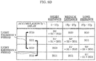
- FIG. 4D illustrates the correlation between the signals accumulated in the charge accumulation transistors (SGO, SG1, SG2, and SG3) and the distance measurement ranges.
- reflected-light signal S0' is accumulated in the charge accumulation transistor (SG0)
- reflected-light signal S1' is accumulated in the charge accumulation transistor (SG1)
- background-light signal BG0 is accumulated in the charge accumulation transistor (SG2)
- background-light signal BG1 is accumulated in the charge accumulation transistor (SG3).
- the signal amount of S0' and S1' (the reflected-light signals) is greater than that of BG0 and BG1 (the background-light signals), and thus, by determining a combination of two charge accumulation transistors (SG) having a great amount of signals, it is possible to use different distance measurement calculation expressions for short, medium, and long distances with reference to the table illustrated in FIG. 4D , which enables seamless distance measurement covering a wide range from a short distance to a long distance.
- Distance measurement calculation expressions for obtaining distance L to object 600 at short, medium, and long distances are shown below.
- read gate TG0 and exposure reset gate PRS0 are set to VH, and all the signal charge resulting from photoelectrical conversion by photoelectric conversion element 1A is discharged to the drain (VPRD) via exposure reset gate PRS0.
- read gate TG0 is switched ON (VH) first, and after a lapse of a certain period P2, exposure reset gate PRS0 is switched OFF (VL).
- both read gate TG0 and exposure reset gate PRS0 are ON (VH), but the potential of exposure reset gate PRS0 is set higher than the potential of read gate TG0.
- the threshold voltage of exposure reset gate PRS0 is set lower than the threshold voltage of read gate TG0. Examples of this approach include setting the p-type impurity concentration of exposure reset gate PRS0 lower than the p-type impurity concentration of read gate TG0.
- a direct-current (DC) voltage of approximately 0 to (VH-VL)/2 may be superimposed on exposure reset gate PRS0.
- DC direct-current
- Examples of this approach include setting high-level potential VH' of exposure reset gate PRS0 higher than potential VH of read gate TG0.
- read gate TG0 is ON and exposure reset gate PRS0 is OFF, and all the signal charge resulting from photoelectrical conversion by photoelectric conversion element 1A is transferred, via read gate TG0, to the charge accumulation transistor (SG0), and accumulated therein; thus, the exposure in the 0 to 1 Tp period is performed.
- exposure reset gate PRS0 is switched ON, and after a lapse of a certain period P4, read gate TG0 is switched OFF; thus, the first exposure sequence is completed.
- the state of potential in period P4 is the same as the state of potential in period P2
- the state of potential in period P5 is the same as the state of potential in period P1; the same or similar operations are performed.
- Embodiment 1 the case is assumed in which light is repeatedly emitted in such a manner that the interval between the start of emission of an irradiating pulsed beam and the next start of the light emission is longer than 4 Tp.
- the present variation describes a drive method in which the interval between the start of emission of an irradiating pulsed beam and the next start of the light emission is set to 4 Tp, and the light emission and the exposure are repeatedly performed on a 4-Tp cycle.
- FIG. 7A is a distance measurement drive timing chart for longer-distance object measurement of a solid-state imaging device according to a variation of Embodiment 1.
- FIG. 7B additionally illustrates a combination of signals obtained by the longer-distance object measurement.
- FIG. 7A illustrates the case of an object in which delay time of the reflected light is 3 Tp to 4 Tp (longer distance), and the distance measurement calculation table applied at this time is as illustrated in the table in FIG. 7B .
- the charge accumulation transistor (SG3) and the charge accumulation transistor (SG0) can obtain S0' and S1' even if the delay amount of the reflected light is between 3 Tp and 4 Tp.
- FIG. 8 illustrates a circuit configuration of a distance measurement pixel of a solid-state imaging device according to Embodiment 2.
- distance measurement pixel 11 includes: one unit pixel 11A which receives reflected light, photoelectrically converts the reflected light into signal charge, and accumulates and outputs the signal charge; one FD 21 which converts the signal charge into a voltage; reset (RST) transistor 24 which discharges the signal charge of FD 21 to a reset drain (VRD); amplification transistor 23 which is connected to a VDD power supply and amplifies a signal from FD 21; and selection (SEL) transistor 25 which outputs and controls a signal from amplification transistor 23 in accordance with an exteriorly obtained selection signal.
- RST reset
- VRD reset drain
- amplification transistor 23 which is connected to a VDD power supply and amplifies a signal from FD 21
- selection (SEL) transistor 25 which outputs and controls a signal from amplification transistor 23 in accordance with an exteriorly obtained selection signal.
- One unit pixel 11A includes: one light receiver which receives the reflected light and photoelectrically converts the received light; one charge reset transistor which discharges, to a charge discharger, a signal obtained from the light receiver; four read transistors which read the signal from the light receiver; four charge accumulation transistors which accumulate the signal read by the four read transistors; and one, two, or four output transistors which output the signal accumulated in the charge accumulation transistors ( FIG. 8 illustrates the case where four output transistors are provided).
- unit pixel 11A includes one photoelectric conversion element 1, read gates TG0, TG2, TG1, and TG3, charge accumulation gates SG0, SG2, SG1, and SG3, output gates OG0, OG2, OG1, and OG3, and charge reset gate PRS.
- the number of read gates TG and the number of charge accumulation gates SG are unchanged, but the number of photoelectric conversion elements and the number of charge reset gates PRS are each reduced from two to one. Therefore, the area of the photoelectric conversion element can be approximately doubled, and the sensitivity per photoelectric conversion element is increased about twofold.
- charge reset gate PRS In order to determine the distance measurement exposure time, charge reset gate PRS needs to be switched ON and OFF at a pulse width of several ns to several hundred ns. Especially, when a short pulse width is required to improve the distance measurement accuracy, the rising edge time and the falling edge time need be no greater than several ns.
- a typical solution to this issue is to increase the width of a metal wire or provide multiple wires so that the resistance is reduced, but this causes problems such as a smaller aperture of the photoelectric conversion element and a reduction in sensitivity.
- the photoelectric conversion element can be formed with a wide aperture, compared to that in Embodiment 1.
- the sensitivity per photoelectric conversion element can be increased twofold or more.
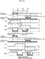
- FIG. 9A is a distance measurement drive timing chart for short-distance object measurement of the solid-state imaging device according to Embodiment 2.
- FIG. 9B is a distance measurement drive timing chart for medium-distance object measurement of the solid-state imaging device according to Embodiment 2.
- FIG. 9C is a distance measurement drive timing chart for long-distance object measurement of the solid-state imaging device according to Embodiment 2.
- FIG. 9D illustrates combinations of signals obtained by the short-distance object measurement, the medium-distance object measurement, and the long-distance object measurement.
- FIG. 10 illustrates comparison between sequences of light emission, exposure, and reading in distance measurement driving.
- drive controller 300 switches OFF read gate TG0 of unit pixel 11A and switches ON exposure reset gate PRS0 of unit pixel 11A.
- the signal charge of photoelectric conversion element 1 is discharged to drain VPRD.
- drive controller 300 switches ON read gate TG0 (VL to VH).
- drive controller 300 causes exposure reset gate PRS to transition to OFF (VH to VL) in synchronization with the start of emission of the first irradiating pulsed beam (light emission 1). With this, the first exposure of photoelectric conversion element 1 is started.
- drive controller 300 causes exposure reset gate PRS to transition to ON (VL to VH) in synchronization with the end of the emission of the first irradiating pulsed beam (light emission 1). With this, the first exposure of photoelectric conversion element 1 is completed.
- drive controller 300 causes read gate TG0 to transition to OFF (VH to VL).
- the first exposure sequence is completed.
- the first exposure sequence corresponds to the first exposure operation of photoelectric conversion element 1 of unit pixel 11A in periods P1 to P5.
- drive controller 300 causes exposure reset gate PRS to transition to OFF (VH to VL) at a point in time when period Tp has elapsed since exposure reset gate PRS is switched ON in the first exposure sequence. With this, the second exposure of photoelectric conversion element 1 is started.
- drive controller 300 causes exposure reset gate PRS to transition to ON (VL to VH) at a point in time when period Tp (the second predetermined period of time) has elapsed since exposure reset gate PRS is switched OFF. With this, the second exposure of photoelectric conversion element 1 is completed.
- drive controller 300 causes read gate TG2 to transition to OFF (VH to VL).
- the third exposure sequence is completed.
- the third exposure sequence corresponds to the second exposure operation of photoelectric conversion element 1 of unit pixel 11A.
- drive controller 300 causes exposure reset gate PRS to transition to OFF (VH to VL) in synchronization with the end of emission of the second irradiating pulsed beam (light emission 2). With this, the third exposure of photoelectric conversion element 1 is started.
- drive controller 300 causes exposure reset gate PRS to transition to ON (VL to VH) at a point in time when period Tp (the third predetermined period of time) has elapsed since exposure reset gate PRS is switched OFF. With this, the third exposure of photoelectric conversion element 1 is completed.
- drive controller 300 causes read gate TG1 to transition to OFF (VH to VL).
- the second exposure sequence is completed.
- the second exposure sequence corresponds to the third exposure operation of photoelectric conversion element 1 of unit pixel 11A.
- drive controller 300 causes exposure reset gate PRS to transition to OFF (VH to VL) at a point in time when period Tp has elapsed since exposure reset gate PRS is switched ON in the second exposure sequence. With this, the fourth exposure of photoelectric conversion element 1 is started.
- drive controller 300 causes exposure reset gate PRS to transition to ON (VL to VH) at a point in time when period Tp (the third predetermined period of time) has elapsed since exposure reset gate PRS is switched OFF. With this, the fourth exposure of photoelectric conversion element 1 is completed.
- drive controller 300 causes read gate TG3 to transition to OFF (VH to VL).
- the fourth exposure sequence is completed.
- the fourth exposure sequence corresponds to the fourth exposure operation of photoelectric conversion element 1 of unit pixel 11A.
- the first exposure sequence, the third exposure sequence, the second exposure sequence, and the fourth exposure sequence are sequentially performed, and thus drive controller 300 obtains a signal necessary for distance measurement.
- the sensitivity per photoelectric conversion element is increased to a value greater than or equal to twice that in Embodiment 1, and therefore the length of emission of the first irradiating pulsed beam (light emission 1) and the length of emission of the second irradiating pulsed beam (light emission 2) can each be reduced to half or less.
- the total length of light emission can be kept to less than or equal to the total length of light emission in the related art and Embodiment 1.
- the second irradiating pulsed beam (light emission 2) preferably has the same pulse width as the first irradiating pulsed beam (light emission 2).
- the first irradiating pulsed beam (light emission 1) is repeated several hundred to several million times, and then the second irradiating pulsed beam (light emission 2) is repeated the same number of times before the transition to reading.
- light emission 1 and light emission 2 which are repeated a small number of times may be alternately performed plural times before the transition to reading (Variation of Embodiment 2).
- the temporal difference between the exposure in light emission 1 and the exposure in light emission 2 can be smaller than that in Embodiment 2.
- distance measurement error on an edge portion of the object due to this temporal difference can be inhibited.
- the distance measurement calculation expressions for determining distance L to object 600 at short, medium, and long distances according to the present embodiment and the variation thereof are the same as those in Equations 5 to 10 indicated in Embodiment 1.
- reflected-light signal S0' is accumulated in the charge accumulation transistor (SG0)
- reflected-light signal S1' is accumulated in the charge accumulation transistor (SG1)
- background-light signal BG0 is accumulated in the charge accumulation transistor (SG2)
- background-light signal BG1 is accumulated in the charge accumulation transistor (SG3).
- the signal amount of S0' and S1' (the reflected-light signals) is greater than that of BG0 and BG1 (the background-light signals), and thus, by determining a combination of two charge accumulation transistors (SG) having a great amount of signals, it is possible to use different distance measurement calculation expressions for short, medium, and long distances with reference to the table illustrated in FIG. 9D , which enables seamless distance measurement covering a wide range from a short distance to a long distance.
- FIG. 11 illustrates transitions of a pixel potential distribution at the time of distance measurement driving of a unit pixel according to Embodiment 2.
- the potential change of the unit pixel at the time of exposure according to Embodiment 2 is basically the same as that according to Embodiment 1.
- read gate TG0 is set to VL
- exposure reset gate PRS is set to VH
- all the signal charge resulting from photoelectrical conversion by photoelectric conversion element 1 is discharged to the drain (VPRD) via exposure reset gate PRS.
- read gate TG0 is switched ON (VH) first, and after a lapse of a certain period P2, exposure reset gate PRS is switched OFF (VL).
- the threshold voltage of exposure reset gate PRS is set lower than the threshold voltage of read gate TG0.
- this approach include setting the p-type impurity concentration of exposure reset gate PRS lower than the p-type impurity concentration of read gate TG0.
- a DC voltage of approximately 0 to (VH-VL)/2 may be superimposed on exposure reset gate PRS0. Examples of this approach include setting high-level potential VH' of exposure reset gate PRS0 higher than potential VH of read gate TG0.
- read gate TG0 is ON and exposure reset gate PRS is OFF, and all the signal charge resulting from photoelectrical conversion by photoelectric conversion element 1 is transferred, via read gate TG0, to the charge accumulation transistor (SG0), and accumulated therein; thus, the exposure in the 0 to 1 Tp period is performed.
- exposure reset gate PRS is switched ON, and after a lapse of a certain period P4, read gate TG0 is switched OFF; thus, the first exposure sequence is completed.
- the state of potential in period P4 is the same as the state of potential in period P2
- the state of potential in period P5 is the same as the state of potential in period P1; the same or similar operations are performed.
- FIG. 13A is a distance measurement drive timing chart for longer-distance object measurement of a solid-state imaging device according to a variation of Embodiment 2.
- FIG. 13B additionally illustrates a combination of signals obtained by the longer-distance object measurement.
- FIG. 13A illustrates the case of an object in which delay time of the reflected light is 3 Tp to 4 Tp (longer distance), and the distance measurement calculation table applied at this time is as illustrated in the table in FIG. 13B .
- Embodiment 2 describes the case where light is repeatedly emitted in such a manner that the interval between the start of light emission and the next start of the light emission is longer than 4 Tp
- the present variation describes the case where the interval between the start of light emission and the next start of the light emission is set to 4 Tp, and the light emission and the exposure are repeatedly performed on a 4-Tp cycle.
- the charge accumulation transistor (SG3) and the charge accumulation transistor (SG0) can obtain S0' and S1' even if the delay amount of the reflected light is between 3 Tp and 4 Tp.
- the charge reset transistor which discharges, to the charge discharger, the signal obtained from the light receiver in the unit pixel according to Embodiment 2 is formed of a metal-oxide-semiconductor (MOS) transistor including an insulating film and a gate electrode film formed above the semiconductor substrate, but this charge reset transistor may be formed of an npn bipolar transistor, which is often used in an interline-transfer capacitive coupling element, as illustrated in FIG. 14 .
- MOS metal-oxide-semiconductor
- FIG. 14 illustrates a cross-sectional structure of a unit pixel according to another embodiment.
- n-type photoelectric conversion element 1A PDO
- p-well serves as a base portion
- VSUB n-type substrate electrode
- the p-well of the base portion is grounded, and when high-level voltage VH' is applied to the n-type substrate electrode (VSUB) of the collector portion, the signal charge resulting from photoelectric conversion by photoelectric conversion element 1A is discharged to n-type substrate electrode VSUB via the p-well.
- the parasitic capacitance between the p-well and substrate electrode VSUB is significantly reduced, compared to the parasitic capacitance between exposure reset gate PRSO and the drain (VPRD) according to Embodiment 2, and furthermore, when the n-type substrate electrode has a high n-type impurity concentration, the substrate resistance of the n-type substrate electrode is significantly reduced; thus, it is possible to make significant improvements to the roundness of the waveform of exposure reset pulse, the delayed timing, etc., that are caused by such parasitic capacitance and substrate resistance.
- Embodiment 2 there is no need to form exposure reset gate PRSO and the drain (VPRD) adjacent to photoelectric conversion element 1A, the area, aperture, etc., of photoelectric conversion element 1A can be widened, and thus more improvements to the sensitivity and the saturation are possible than in Embodiment 2.
- PRSO and the drain VPRD
- the abovementioned plurality of unit pixels may include m unit pixels each of which performs the exposure sequence n times to obtain a maximum of m ⁇ n signals having different exposure periods.
- the present invention is useful, for example, for a gesture user interface which detects movement of a person, an intrusion detection sensor which detects an object, a person, or the like entering the distance measurement range, and a three-dimensional input device which collects accurate data on the shape of an object in real-time.
Landscapes
- Engineering & Computer Science (AREA)
- Physics & Mathematics (AREA)
- General Physics & Mathematics (AREA)
- Computer Networks & Wireless Communication (AREA)
- Radar, Positioning & Navigation (AREA)
- Remote Sensing (AREA)
- Electromagnetism (AREA)
- Signal Processing (AREA)
- Multimedia (AREA)
- Optical Radar Systems And Details Thereof (AREA)
- Transforming Light Signals Into Electric Signals (AREA)
- Solid State Image Pick-Up Elements (AREA)
- Measurement Of Optical Distance (AREA)
Claims (18)
- Verfahren zum Ansteuern einer Festkörper-Bildgebungsvorrichtung (1000), die ein Abstandsmessbild zum Messen eines Abstands zu einem Objekt (600) erfasst, das mit einem gepulsten Strahl mit einer vorbestimmten Impulsbreite bestrahlt wird und eine Vielzahl von Pixeln (10A, 10B) einschließlich mindestens eines ersten Pixels auf einem Halbleitersubstrat einschließt, wobei das erste Pixel (10A) einschließt:einen photoelektrischen Wandler (1A), der von dem Objekt (600) reflektiertes Licht empfängt und das reflektierte Licht in Ladung umwandelt;einen Ladungsentlader (VPRD), der die Ladung des photoelektrischen Wandlers entlädt;ein Belichtungs-Rücksetzgatter (PRSO), das zwischen dem Timing für die Akkumulation der Ladung in dem photoelektrischen Wandler (1A) und dem Timing für die Entladung der Ladung aus dem photoelektrischen Wandler (1A) zum Ladungsentlader (VPRD) umschaltet;eine Vielzahl von Ladungsspeichern (SGO, SG2), die die Ladung des photoelektrischen Wandlers (1A) akkumulieren; undeine Vielzahl von Lesegattern (TGO, TG2), die zwischen dem photoelektrischen Wandler (1A) und der Vielzahl von Ladungsspeichern (SGO, SG2) vorgesehen sind und die Ladung aus dem photoelektrischen Wandler (1A) lesen und mindestens ein erstes Lesegatter (TG0) und ein zweites Lesegatter (TG2) einschließen, wobei das Verfahren zum Ansteuern der Festkörper-Bildgebungsvorrichtung (1000) umfasst:Durchführen einer ersten Belichtung als die Belichtung, die in einer ersten Periode durchgeführt wird, in der ein Gatter des ersten Lesegatters (TG0) in den leitenden Zustand eingeschaltet wird; undDurchführen einer zweiten Belichtung als die Belichtung, die in einer zweiten Periode durchgeführt wird, die in Verbindung mit einem Ende der ersten Periode gestartet wird und in der ein Gatter des zweiten Lesegatters (TG2) in den leitenden Zustand eingeschaltet wird;Starten der Belichtung des photoelektrischen Wandlers (1A), indem das Belichtungs-Rücksetzgatter (PRSO) nach dem Ablauf einer vorbestimmten Zeitspanne, die beginnt, wenn eines der Lesegatter (TGO, TG2) in einen leitenden Zustand versetzt wird, in einen nichtleitenden Zustand ausgeschaltet wird;Stoppen der Belichtung des photoelektrischen Wandlers (1A), indem das Belichtungs-Rücksetzgatter (PRSO) eine vorbestimmte Zeitspanne vor dem Ausschalten des jeweiligen Lesegatters (TGO, TG2) in den nichtleitenden Zustand, nachdem die Belichtung gestartet wird, in den leitenden Zustand eingeschaltet wird.
- Verfahren zum Ansteuern der Festkörper-Bildgebungsvorrichtung nach Anspruch 1,
wobei die erste Belichtung in einer Periode durchgeführt wird, die eine Periode überlappt, in der der gepulste Strahl emittiert wird, und
die zweite Belichtung in einer Periode durchgeführt wird, in der der gepulste Strahl nicht emittiert wird. - Verfahren zum Ansteuern der Festkörper-Bildgebungsvorrichtung nach einem der Ansprüche 1 und 2,
wobei eine Dauer der zweiten Belichtung gleich einer Dauer der ersten Belichtung ist. - Verfahren zum Ansteuern der Festkörper-Bildgebungsvorrichtung nach einem der Ansprüche 1 bis 3,
wobei die Vielzahl von Pixeln weiterhin einschließt mindestens ein zweites Pixel (10B) einschließend: den photoelektrischen Wandler (1B); das Belichtungs-Rücksetzgatter (PRS1); und eine Vielzahl von Lesegattern (TG1, TG3), die die Ladung aus dem photoelektrischen Wandler (1B) lesen und mindestens ein drittes Lesegatter (TG1) und ein viertes Lesegatter (TG3) einschließen, und
das Verfahren zum Ansteuern der Festkörper-Bildgebungsvorrichtung (1000) umfasst:Durchführen einer dritten Belichtung als die Belichtung, die in einer dritten Periode durchgeführt wird, in der ein Gatter des dritten Lesegatters (TG1) eingeschaltet ist; undDurchführen einer vierten Belichtung als die Belichtung, die in einer vierten Periode durchgeführt wird, die in Verbindung mit einem Ende der dritten Periode gestartet wird und in der ein Gatter des vierten Lesegatters (TG3) eingeschaltet ist. - Verfahren zum Ansteuern der Festkörper-Bildgebungsvorrichtung nach Anspruch 4,
wobei in Verbindung mit dem Einschalten eines Gatters des Belichtungs-Rücksetzgatters (PRSO) des ersten Pixels (10A), um die erste Belichtung zu stoppen, ein Gatter des Belichtungs-Rücksetzgatters (PRS1) des zweiten Pixels (10B) ausgeschaltet wird, um die dritte Belichtung zu starten. - Verfahren zum Ansteuern der Festkörper-Bildgebungsvorrichtung nach Anspruch 4 oder 5,
wobei in Verbindung mit dem Einschalten eines Gatters des Belichtungs-Rücksetzgatters (PRSO) des ersten Pixels (10A), um die zweite Belichtung zu stoppen, ein Gatter des Belichtungs-Rücksetzgatters (PRS1) des zweiten Pixels (10B) ausgeschaltet wird, um die vierte Belichtung zu starten. - Verfahren zum Ansteuern der Festkörper-Bildgebungsvorrichtung nach einem der Ansprüche 4 bis 6,
wobei die dritte Belichtung oder die vierte Belichtung durch Ausschalten eines Gatters des Belichtungs-Rücksetzgatters (PRS1) des zweiten Pixels (10B) nach Ablauf einer vorbestimmten Zeitspanne gestartet wird, die beginnt, wenn das Gatter des dritten Lesegatters (TG1) oder des vierten Lesegatters (TG3) eingeschaltet wird, und
nach dem Starten der Belichtung die dritte Belichtung oder die vierte Belichtung gestoppt wird, indem das Gatter des Belichtungs-Rücksetzgatters (PRS1) des zweiten Pixels (10B) eine vorbestimmte Zeitspanne vor dem Ausschalten des Gatters des dritten Lesegatters (TG1) oder des vierten Lesegatters (TG3) eingeschaltet wird. - Verfahren zum Ansteuern der Festkörper-Bildgebungsvorrichtung nach einem der Ansprüche 4 bis 7,
wobei eine Dauer der vierten Belichtung gleich einer Dauer der dritten Belichtung ist. - Verfahren zum Ansteuern der Festkörper-Bildgebungsvorrichtung nach einem der Ansprüche 1 bis 3,
wobei die erste Belichtung in Verbindung mit einem Start der Emission des gepulsten Strahls gestartet wird. - Verfahren zum Ansteuern der Festkörper-Bildgebungsvorrichtung nach einem der Ansprüche 4 bis 8,
wobei die erste Belichtung in Verbindung mit einem Start der Emission des gepulsten Strahls gestartet wird, und
die dritte Belichtung in Verbindung mit einem Ende der Emission des gepulsten Strahls gestartet wird. - Verfahren zum Ansteuern der Festkörper-Bildgebungsvorrichtung nach einem der Ansprüche 1 bis 10,
wobei einem Ansteuerimpulssignal, das dem Belichtungs-Rücksetzgatter (PRSO) zugeführt wird, eine Gleichstrom-(DC)-Vorspannung überlagert ist. - Verfahren zum Ansteuern der Festkörper-Bildgebungsvorrichtung nach einem der Ansprüche 1 bis 11,
wobei das Belichtungs-Rücksetzgatter (PRSO) einen npn-Bipolartransistor einschließt, der in einer Halbleitersubstrattiefenrichtung ausgebildet ist, in der der photoelektrische Wandler ausgebildet ist, und
die Vielzahl von Lesegattern (TGO, TG2) einen MetallOxid-Halbleiter (MOS)-Transistor einschließen. - Verfahren zum Ansteuern der Festkörper-Bildgebungsvorrichtung nach einem der Ansprüche 1 bis 11,
wobei das Belichtungs-Rücksetzgatter (PRSO) und die Vielzahl von Lesegattern (TGO, TG2) einen MOS-Transistor einschließen, und
ein Schwellenwert des MOS-Transistors des Belichtungs-Rücksetzgatters niedriger eingestellt ist als ein Schwellenwert des MOS-Transistors jedes der Vielzahl von Lesegattern. - Verfahren zum Ansteuern der Festkörper-Bildgebungsvorrichtung nach einem der Ansprüche 1 bis 13,
wobei das Belichtungs-Rücksetzgatter (PRSO) eine p-Typ-Diffusionsschichtkonzentration aufweist, die niedriger ist als eine p-Typ-Diffusionsschichtkonzentration jedes der Vielzahl von Lesegattern (TGO, TG2). - Verfahren zum Ansteuern der Festkörper-Bildgebungsvorrichtung nach einem der Ansprüche 1 bis 14,
wobei die Festkörper-Bildgebungsvorrichtung weiterhin einschließt:eine Vielzahl von Ladungsspeichern, die die Ladung des photoelektrischen Wandlers akkumulieren; undeine schwebende Diffusion (21), die ein Ladungssignal in ein Spannungssignal umwandelt. - Verfahren zum Ansteuern der Festkörper-Bildgebungsvorrichtung nach Anspruch 15,
wobei die Vielzahl von Pixeln weiterhin einschließt
eine lichtabschirmende Folie, die die Vielzahl der Ladungsspeicher vor Licht abschirmt. - Verfahren zum Ansteuern der Festkörper-Bildgebungsvorrichtung nach einem der Ansprüche 1 bis 16, weiterhin umfassend
Wiederholen der Belichtung n-mal. - Verfahren zum Ansteuern der Festkörper-Bildgebungsvorrichtung nach einem der Ansprüche 1 bis 17,
wobei die Vielzahl von Pixeln m Pixel einschließt, und
jedes der m Pixel die Belichtung n-mal durchführt, um ein Maximum von mXn Signalen mit unterschiedlichen Belichtungszeiten zu erhalten.
Applications Claiming Priority (2)
| Application Number | Priority Date | Filing Date | Title |
|---|---|---|---|
| JP2015154512 | 2015-08-04 | ||
| PCT/JP2016/003494 WO2017022219A1 (ja) | 2015-08-04 | 2016-07-28 | 固体撮像装置の駆動方法 |
Publications (3)
| Publication Number | Publication Date |
|---|---|
| EP3334151A1 EP3334151A1 (de) | 2018-06-13 |
| EP3334151A4 EP3334151A4 (de) | 2018-08-22 |
| EP3334151B1 true EP3334151B1 (de) | 2021-04-07 |
Family
ID=57942796
Family Applications (1)
| Application Number | Title | Priority Date | Filing Date |
|---|---|---|---|
| EP16832502.5A Active EP3334151B1 (de) | 2015-08-04 | 2016-07-28 | Verfahren zur ansteuerung eines bildsensors |
Country Status (5)
| Country | Link |
|---|---|
| US (1) | US10928493B2 (de) |
| EP (1) | EP3334151B1 (de) |
| JP (1) | JP6799538B2 (de) |
| CN (1) | CN107852470B (de) |
| WO (1) | WO2017022219A1 (de) |
Families Citing this family (27)
| Publication number | Priority date | Publication date | Assignee | Title |
|---|---|---|---|---|
| US10254389B2 (en) | 2015-11-06 | 2019-04-09 | Artilux Corporation | High-speed light sensing apparatus |
| US10418407B2 (en) | 2015-11-06 | 2019-09-17 | Artilux, Inc. | High-speed light sensing apparatus III |
| DE102016208347B4 (de) * | 2016-05-13 | 2017-12-21 | Infineon Technologies Ag | Optische Sensorvorrichtung und Verfahren zum Betreiben eines Laufzeitsensors |
| JP2018185179A (ja) * | 2017-04-25 | 2018-11-22 | 株式会社リコー | 測距装置、監視装置、3次元計測装置、移動体、ロボット及び測距方法 |
| AU2018386190A1 (en) * | 2017-12-13 | 2020-06-04 | Magic Leap, Inc. | Global shutter pixel circuit and method for computer vision applications |
| US11105928B2 (en) | 2018-02-23 | 2021-08-31 | Artilux, Inc. | Light-sensing apparatus and light-sensing method thereof |
| US10886311B2 (en) * | 2018-04-08 | 2021-01-05 | Artilux, Inc. | Photo-detecting apparatus |
| JP7362198B2 (ja) | 2018-07-18 | 2023-10-17 | ソニーセミコンダクタソリューションズ株式会社 | 受光素子、測距モジュール、および、電子機器 |
| CN112513671B (zh) * | 2018-08-02 | 2024-09-06 | 新唐科技日本株式会社 | 摄像装置、在该摄像装置中使用的固体摄像元件及摄像方法 |
| CN108957470B (zh) * | 2018-08-22 | 2021-02-26 | 上海炬佑智能科技有限公司 | 飞行时间测距传感器及其测距方法 |
| WO2020080065A1 (ja) * | 2018-10-16 | 2020-04-23 | 株式会社ブルックマンテクノロジ | 測距装置、カメラ、及び測距装置の駆動調整方法 |
| WO2020178920A1 (ja) * | 2019-03-01 | 2020-09-10 | 株式会社ブルックマンテクノロジ | 距離画像撮像装置および距離画像撮像装置による距離画像撮像方法 |
| JP2020153799A (ja) * | 2019-03-20 | 2020-09-24 | ソニーセミコンダクタソリューションズ株式会社 | 測距装置および測距方法 |
| CN113490862B (zh) * | 2019-03-29 | 2025-10-17 | 新唐科技日本株式会社 | 摄像装置以及差异信息算出方法 |
| DE112020002523T5 (de) * | 2019-05-24 | 2022-03-24 | Sony Semiconductor Solutions Corporation | Festkörper-bildgebungsvorrichtung und abstandsmessvorrichtung |
| JP7463671B2 (ja) * | 2019-08-01 | 2024-04-09 | Toppanホールディングス株式会社 | 距離画像撮像装置、及び距離画像撮像方法 |
| US12278252B2 (en) | 2019-08-28 | 2025-04-15 | Artilux, Inc. | Photo-detecting apparatus with low dark current |
| US12477856B2 (en) | 2019-08-28 | 2025-11-18 | Artilux, Inc. | Photo-detecting apparatus with low dark current |
| JP6824363B1 (ja) | 2019-10-30 | 2021-02-03 | 浜松ホトニクス株式会社 | イメージセンサ、及びイメージセンサの制御方法 |
| KR102887078B1 (ko) | 2019-11-07 | 2025-11-18 | 삼성전자주식회사 | 깊이의 측정 범위에 기초하여 동작하는 센서 및 이를 포함하는 센싱 시스템 |
| JP7638221B2 (ja) * | 2019-11-27 | 2025-03-03 | ヌヴォトンテクノロジージャパン株式会社 | 測距撮像装置 |
| CN114846355B (zh) * | 2020-01-17 | 2025-04-22 | 松下知识产权经营株式会社 | 测距装置 |
| CN111837053B (zh) | 2020-03-25 | 2024-04-26 | 深圳市汇顶科技股份有限公司 | 基于飞行时间的测距方法和测距系统 |
| JP7721260B2 (ja) * | 2020-10-21 | 2025-08-12 | キヤノン株式会社 | 光電変換装置、光電変換システム |
| KR20220073404A (ko) | 2020-11-26 | 2022-06-03 | 삼성전자주식회사 | 복수의 포토다이오드들을 포함하는 거리 픽셀 및 이를 포함하는 비행 거리 센서 |
| EP4020006B1 (de) * | 2020-12-23 | 2025-07-02 | STMicroelectronics (Research & Development) Limited | Time-of-flight sensor |
| TWI830306B (zh) * | 2022-07-27 | 2024-01-21 | 茂達電子股份有限公司 | 具有感測順序調變機制的光感測方法 |
Family Cites Families (13)
| Publication number | Priority date | Publication date | Assignee | Title |
|---|---|---|---|---|
| JP4235729B2 (ja) | 2003-02-03 | 2009-03-11 | 国立大学法人静岡大学 | 距離画像センサ |
| WO2007119626A1 (ja) * | 2006-03-31 | 2007-10-25 | National University Corporation Shizuoka University | 半導体測距素子及び固体撮像装置 |
| EP2587794B1 (de) * | 2008-04-07 | 2022-05-04 | Cmosis NV | Pixel und Pixelarray mit globaler Blende |
| DE102008018718B4 (de) * | 2008-04-14 | 2010-02-25 | Fraunhofer-Gesellschaft zur Förderung der angewandten Forschung e.V. | Optischer Abstandsmesser und Verfahren zur optischen Abstandsmessung |
| JP5404112B2 (ja) | 2009-03-12 | 2014-01-29 | キヤノン株式会社 | 固体撮像素子、その駆動方法及び撮像システム |
| DE102009037596B4 (de) * | 2009-08-14 | 2014-07-24 | Fraunhofer-Gesellschaft zur Förderung der angewandten Forschung e.V. | Pixelstruktur, System und Verfahren zur optischen Abstandsmessung sowie Steuerschaltung für die Pixelstruktur |
| JP5476190B2 (ja) * | 2010-03-31 | 2014-04-23 | 本田技研工業株式会社 | 固体撮像装置 |
| EP2437484B1 (de) * | 2010-10-01 | 2017-02-15 | Sony Semiconductor Solutions Corporation | Abbildungsvorrichtung und Kamerasystem |
| JP5576851B2 (ja) | 2011-12-27 | 2014-08-20 | 本田技研工業株式会社 | 測距システム及び測距方法 |
| JP5876289B2 (ja) * | 2011-12-28 | 2016-03-02 | 浜松ホトニクス株式会社 | 距離測定装置 |
| JP2013195344A (ja) * | 2012-03-22 | 2013-09-30 | Toshiba Corp | 飛行時間型距離センサ |
| WO2014207788A1 (ja) * | 2013-06-27 | 2014-12-31 | パナソニックIpマネジメント株式会社 | 固体撮像素子及び測距撮像装置 |
| CN105899966B (zh) * | 2014-01-14 | 2019-05-07 | 松下知识产权经营株式会社 | 距离图像生成装置以及距离图像生成方法 |
-
2016
- 2016-07-28 JP JP2017532370A patent/JP6799538B2/ja active Active
- 2016-07-28 EP EP16832502.5A patent/EP3334151B1/de active Active
- 2016-07-28 CN CN201680045243.4A patent/CN107852470B/zh active Active
- 2016-07-28 WO PCT/JP2016/003494 patent/WO2017022219A1/ja not_active Ceased
-
2018
- 2018-01-31 US US15/885,436 patent/US10928493B2/en active Active
Non-Patent Citations (1)
| Title |
|---|
| None * |
Also Published As
| Publication number | Publication date |
|---|---|
| US10928493B2 (en) | 2021-02-23 |
| CN107852470B (zh) | 2020-11-03 |
| JPWO2017022219A1 (ja) | 2018-05-31 |
| EP3334151A1 (de) | 2018-06-13 |
| CN107852470A (zh) | 2018-03-27 |
| JP6799538B2 (ja) | 2020-12-16 |
| WO2017022219A1 (ja) | 2017-02-09 |
| EP3334151A4 (de) | 2018-08-22 |
| US20180156899A1 (en) | 2018-06-07 |
Similar Documents
| Publication | Publication Date | Title |
|---|---|---|
| EP3334151B1 (de) | Verfahren zur ansteuerung eines bildsensors | |
| US11769775B2 (en) | Distance-measuring imaging device, distance measuring method of distance-measuring imaging device, and solid-state imaging device | |
| US10690755B2 (en) | Solid-state imaging device having increased distance measurement accuracy and increased distance measurement range | |
| KR101508410B1 (ko) | 거리 화상 센서, 및 촬상 신호를 비행시간법에 의해 생성하는 방법 | |
| EP3474038B1 (de) | Bildsensor zur bestimmung eines dreidimensionalen bildes und verfahren zur bestimmung eines dreidimensionalen bildes | |
| US8792087B2 (en) | Concept for optical distance measurement | |
| US7683954B2 (en) | Solid-state image sensor | |
| US20180246214A1 (en) | Solid-state imaging device, distance measurement device, and distance measurement method | |
| EP3334152B1 (de) | Festkörperbildgebungsvorrichtung | |
| US8947645B2 (en) | Photoelectric conversion element, light receiving device, light receiving system, and distance measuring device | |
| US20150092019A1 (en) | Image capture device | |
| US8947646B2 (en) | Photoelectric conversion element, light receiving device, light receiving system, and distance measuring device | |
| US20120200841A1 (en) | Photoelectric conversion element, light receiving device, light receiving system, and distance measuring device | |
| JP2010096730A (ja) | 測距システム及び測距方法 | |
| US20220003876A1 (en) | Distance image obtaining method and distance detection device | |
| US11194025B2 (en) | Solid-state imaging device and imaging apparatus including same | |
| JP6735515B2 (ja) | 固体撮像装置 | |
| WO2022137685A1 (ja) | 測距装置、測距方法および位相検出装置 | |
| Durini et al. | CMOS pixels for pulsed 3D time-of-flight sensors | |
| HK1123353A1 (en) | Spatial information detecting device and photodetector suitable therefor | |
| HK1123353B (en) | Spatial information detecting device and photodetector suitable therefor |
Legal Events
| Date | Code | Title | Description |
|---|---|---|---|
| STAA | Information on the status of an ep patent application or granted ep patent |
Free format text: STATUS: THE INTERNATIONAL PUBLICATION HAS BEEN MADE |
|
| PUAI | Public reference made under article 153(3) epc to a published international application that has entered the european phase |
Free format text: ORIGINAL CODE: 0009012 |
|
| STAA | Information on the status of an ep patent application or granted ep patent |
Free format text: STATUS: REQUEST FOR EXAMINATION WAS MADE |
|
| 17P | Request for examination filed |
Effective date: 20180125 |
|
| AK | Designated contracting states |
Kind code of ref document: A1 Designated state(s): AL AT BE BG CH CY CZ DE DK EE ES FI FR GB GR HR HU IE IS IT LI LT LU LV MC MK MT NL NO PL PT RO RS SE SI SK SM TR |
|
| AX | Request for extension of the european patent |
Extension state: BA ME |
|
| A4 | Supplementary search report drawn up and despatched |
Effective date: 20180720 |
|
| RIC1 | Information provided on ipc code assigned before grant |
Ipc: G01S 17/89 20060101ALI20180716BHEP Ipc: H01L 27/146 20060101ALI20180716BHEP Ipc: H04N 5/374 20110101ALI20180716BHEP Ipc: G01S 17/10 20060101ALI20180716BHEP Ipc: G01S 7/486 20060101ALI20180716BHEP Ipc: H04N 5/353 20110101AFI20180716BHEP |
|
| DAV | Request for validation of the european patent (deleted) | ||
| DAX | Request for extension of the european patent (deleted) | ||
| STAA | Information on the status of an ep patent application or granted ep patent |
Free format text: STATUS: EXAMINATION IS IN PROGRESS |
|
| 17Q | First examination report despatched |
Effective date: 20200513 |
|
| RAP1 | Party data changed (applicant data changed or rights of an application transferred) |
Owner name: PANASONIC SEMICONDUCTOR SOLUTIONS CO., LTD. |
|
| REG | Reference to a national code |
Ref country code: DE Ref legal event code: R079 Ref document number: 602016055792 Country of ref document: DE Free format text: PREVIOUS MAIN CLASS: H04N0005353000 Ipc: G01S0007486500 |
|
| GRAP | Despatch of communication of intention to grant a patent |
Free format text: ORIGINAL CODE: EPIDOSNIGR1 |
|
| STAA | Information on the status of an ep patent application or granted ep patent |
Free format text: STATUS: GRANT OF PATENT IS INTENDED |
|
| RIC1 | Information provided on ipc code assigned before grant |
Ipc: G01S 7/4865 20200101AFI20201119BHEP Ipc: G01S 7/4863 20200101ALI20201119BHEP Ipc: H01L 27/148 20060101ALI20201119BHEP Ipc: G01S 17/894 20200101ALI20201119BHEP |
|
| INTG | Intention to grant announced |
Effective date: 20201217 |
|
| RIN1 | Information on inventor provided before grant (corrected) |
Inventor name: SUZUKI, SEI Inventor name: YAMADA, TOHRU Inventor name: SHIMIZU, YASUYUKI |
|
| GRAS | Grant fee paid |
Free format text: ORIGINAL CODE: EPIDOSNIGR3 |
|
| GRAA | (expected) grant |
Free format text: ORIGINAL CODE: 0009210 |
|
| STAA | Information on the status of an ep patent application or granted ep patent |
Free format text: STATUS: THE PATENT HAS BEEN GRANTED |
|
| AK | Designated contracting states |
Kind code of ref document: B1 Designated state(s): AL AT BE BG CH CY CZ DE DK EE ES FI FR GB GR HR HU IE IS IT LI LT LU LV MC MK MT NL NO PL PT RO RS SE SI SK SM TR |
|
| REG | Reference to a national code |
Ref country code: GB Ref legal event code: FG4D |
|
| REG | Reference to a national code |
Ref country code: AT Ref legal event code: REF Ref document number: 1380386 Country of ref document: AT Kind code of ref document: T Effective date: 20210415 Ref country code: CH Ref legal event code: EP |
|
| REG | Reference to a national code |
Ref country code: DE Ref legal event code: R096 Ref document number: 602016055792 Country of ref document: DE |
|
| REG | Reference to a national code |
Ref country code: IE Ref legal event code: FG4D |
|
| REG | Reference to a national code |
Ref country code: DE Ref legal event code: R082 Ref document number: 602016055792 Country of ref document: DE Representative=s name: NOVAGRAAF BREVETS, FR Ref country code: DE Ref legal event code: R081 Ref document number: 602016055792 Country of ref document: DE Owner name: NUVOTON TECHNOLOGY CORPORATION JAPAN, NAGAOKAK, JP Free format text: FORMER OWNER: PANASONIC SEMICONDUCTOR SOLUTIONS CO., LTD., NAGAOKAKYO-SHI, KYOTO, JP Ref country code: DE Ref legal event code: R081 Ref document number: 602016055792 Country of ref document: DE Owner name: NUVOTON TECHNOLOGY CORPARATION JAPAN, NAGAOKAK, JP Free format text: FORMER OWNER: PANASONIC SEMICONDUCTOR SOLUTIONS CO., LTD., NAGAOKAKYO-SHI, KYOTO, JP |
|
| RAP4 | Party data changed (patent owner data changed or rights of a patent transferred) |
Owner name: NUVOTON TECHNOLOGY CORPORATION JAPAN |
|
| REG | Reference to a national code |
Ref country code: DE Ref legal event code: R082 Ref document number: 602016055792 Country of ref document: DE Representative=s name: NOVAGRAAF BREVETS, FR Ref country code: DE Ref legal event code: R081 Ref document number: 602016055792 Country of ref document: DE Owner name: NUVOTON TECHNOLOGY CORPORATION JAPAN, NAGAOKAK, JP Free format text: FORMER OWNER: NUVOTON TECHNOLOGY CORPARATION JAPAN, NAGAOKAKYO-SHI, KYOTO, JP |
|
| REG | Reference to a national code |
Ref country code: LT Ref legal event code: MG9D |
|
| RAP4 | Party data changed (patent owner data changed or rights of a patent transferred) |
Owner name: NUVOTON TECHNOLOGY CORPORATION JAPAN |
|
| REG | Reference to a national code |
Ref country code: NL Ref legal event code: MP Effective date: 20210407 Ref country code: AT Ref legal event code: MK05 Ref document number: 1380386 Country of ref document: AT Kind code of ref document: T Effective date: 20210407 |
|
| PG25 | Lapsed in a contracting state [announced via postgrant information from national office to epo] |
Ref country code: FI Free format text: LAPSE BECAUSE OF FAILURE TO SUBMIT A TRANSLATION OF THE DESCRIPTION OR TO PAY THE FEE WITHIN THE PRESCRIBED TIME-LIMIT Effective date: 20210407 Ref country code: LT Free format text: LAPSE BECAUSE OF FAILURE TO SUBMIT A TRANSLATION OF THE DESCRIPTION OR TO PAY THE FEE WITHIN THE PRESCRIBED TIME-LIMIT Effective date: 20210407 Ref country code: HR Free format text: LAPSE BECAUSE OF FAILURE TO SUBMIT A TRANSLATION OF THE DESCRIPTION OR TO PAY THE FEE WITHIN THE PRESCRIBED TIME-LIMIT Effective date: 20210407 Ref country code: AT Free format text: LAPSE BECAUSE OF FAILURE TO SUBMIT A TRANSLATION OF THE DESCRIPTION OR TO PAY THE FEE WITHIN THE PRESCRIBED TIME-LIMIT Effective date: 20210407 Ref country code: BG Free format text: LAPSE BECAUSE OF FAILURE TO SUBMIT A TRANSLATION OF THE DESCRIPTION OR TO PAY THE FEE WITHIN THE PRESCRIBED TIME-LIMIT Effective date: 20210707 Ref country code: NL Free format text: LAPSE BECAUSE OF FAILURE TO SUBMIT A TRANSLATION OF THE DESCRIPTION OR TO PAY THE FEE WITHIN THE PRESCRIBED TIME-LIMIT Effective date: 20210407 |
|
| PG25 | Lapsed in a contracting state [announced via postgrant information from national office to epo] |
Ref country code: PT Free format text: LAPSE BECAUSE OF FAILURE TO SUBMIT A TRANSLATION OF THE DESCRIPTION OR TO PAY THE FEE WITHIN THE PRESCRIBED TIME-LIMIT Effective date: 20210809 Ref country code: PL Free format text: LAPSE BECAUSE OF FAILURE TO SUBMIT A TRANSLATION OF THE DESCRIPTION OR TO PAY THE FEE WITHIN THE PRESCRIBED TIME-LIMIT Effective date: 20210407 Ref country code: NO Free format text: LAPSE BECAUSE OF FAILURE TO SUBMIT A TRANSLATION OF THE DESCRIPTION OR TO PAY THE FEE WITHIN THE PRESCRIBED TIME-LIMIT Effective date: 20210707 Ref country code: SE Free format text: LAPSE BECAUSE OF FAILURE TO SUBMIT A TRANSLATION OF THE DESCRIPTION OR TO PAY THE FEE WITHIN THE PRESCRIBED TIME-LIMIT Effective date: 20210407 Ref country code: RS Free format text: LAPSE BECAUSE OF FAILURE TO SUBMIT A TRANSLATION OF THE DESCRIPTION OR TO PAY THE FEE WITHIN THE PRESCRIBED TIME-LIMIT Effective date: 20210407 Ref country code: LV Free format text: LAPSE BECAUSE OF FAILURE TO SUBMIT A TRANSLATION OF THE DESCRIPTION OR TO PAY THE FEE WITHIN THE PRESCRIBED TIME-LIMIT Effective date: 20210407 Ref country code: GR Free format text: LAPSE BECAUSE OF FAILURE TO SUBMIT A TRANSLATION OF THE DESCRIPTION OR TO PAY THE FEE WITHIN THE PRESCRIBED TIME-LIMIT Effective date: 20210708 Ref country code: IS Free format text: LAPSE BECAUSE OF FAILURE TO SUBMIT A TRANSLATION OF THE DESCRIPTION OR TO PAY THE FEE WITHIN THE PRESCRIBED TIME-LIMIT Effective date: 20210807 |
|
| REG | Reference to a national code |
Ref country code: DE Ref legal event code: R097 Ref document number: 602016055792 Country of ref document: DE |
|
| PG25 | Lapsed in a contracting state [announced via postgrant information from national office to epo] |
Ref country code: SM Free format text: LAPSE BECAUSE OF FAILURE TO SUBMIT A TRANSLATION OF THE DESCRIPTION OR TO PAY THE FEE WITHIN THE PRESCRIBED TIME-LIMIT Effective date: 20210407 Ref country code: SK Free format text: LAPSE BECAUSE OF FAILURE TO SUBMIT A TRANSLATION OF THE DESCRIPTION OR TO PAY THE FEE WITHIN THE PRESCRIBED TIME-LIMIT Effective date: 20210407 Ref country code: RO Free format text: LAPSE BECAUSE OF FAILURE TO SUBMIT A TRANSLATION OF THE DESCRIPTION OR TO PAY THE FEE WITHIN THE PRESCRIBED TIME-LIMIT Effective date: 20210407 Ref country code: ES Free format text: LAPSE BECAUSE OF FAILURE TO SUBMIT A TRANSLATION OF THE DESCRIPTION OR TO PAY THE FEE WITHIN THE PRESCRIBED TIME-LIMIT Effective date: 20210407 Ref country code: CZ Free format text: LAPSE BECAUSE OF FAILURE TO SUBMIT A TRANSLATION OF THE DESCRIPTION OR TO PAY THE FEE WITHIN THE PRESCRIBED TIME-LIMIT Effective date: 20210407 Ref country code: EE Free format text: LAPSE BECAUSE OF FAILURE TO SUBMIT A TRANSLATION OF THE DESCRIPTION OR TO PAY THE FEE WITHIN THE PRESCRIBED TIME-LIMIT Effective date: 20210407 Ref country code: DK Free format text: LAPSE BECAUSE OF FAILURE TO SUBMIT A TRANSLATION OF THE DESCRIPTION OR TO PAY THE FEE WITHIN THE PRESCRIBED TIME-LIMIT Effective date: 20210407 |
|
| PLBE | No opposition filed within time limit |
Free format text: ORIGINAL CODE: 0009261 |
|
| STAA | Information on the status of an ep patent application or granted ep patent |
Free format text: STATUS: NO OPPOSITION FILED WITHIN TIME LIMIT |
|
| REG | Reference to a national code |
Ref country code: CH Ref legal event code: PL |
|
| 26N | No opposition filed |
Effective date: 20220110 |
|
| GBPC | Gb: european patent ceased through non-payment of renewal fee |
Effective date: 20210728 |
|
| PG25 | Lapsed in a contracting state [announced via postgrant information from national office to epo] |
Ref country code: MC Free format text: LAPSE BECAUSE OF FAILURE TO SUBMIT A TRANSLATION OF THE DESCRIPTION OR TO PAY THE FEE WITHIN THE PRESCRIBED TIME-LIMIT Effective date: 20210407 |
|
| REG | Reference to a national code |
Ref country code: BE Ref legal event code: MM Effective date: 20210731 |
|
| PG25 | Lapsed in a contracting state [announced via postgrant information from national office to epo] |
Ref country code: LI Free format text: LAPSE BECAUSE OF NON-PAYMENT OF DUE FEES Effective date: 20210731 Ref country code: GB Free format text: LAPSE BECAUSE OF NON-PAYMENT OF DUE FEES Effective date: 20210728 Ref country code: CH Free format text: LAPSE BECAUSE OF NON-PAYMENT OF DUE FEES Effective date: 20210731 |
|
| PG25 | Lapsed in a contracting state [announced via postgrant information from national office to epo] |
Ref country code: IS Free format text: LAPSE BECAUSE OF FAILURE TO SUBMIT A TRANSLATION OF THE DESCRIPTION OR TO PAY THE FEE WITHIN THE PRESCRIBED TIME-LIMIT Effective date: 20210807 Ref country code: LU Free format text: LAPSE BECAUSE OF NON-PAYMENT OF DUE FEES Effective date: 20210728 Ref country code: FR Free format text: LAPSE BECAUSE OF NON-PAYMENT OF DUE FEES Effective date: 20210731 Ref country code: AL Free format text: LAPSE BECAUSE OF FAILURE TO SUBMIT A TRANSLATION OF THE DESCRIPTION OR TO PAY THE FEE WITHIN THE PRESCRIBED TIME-LIMIT Effective date: 20210407 |
|
| PG25 | Lapsed in a contracting state [announced via postgrant information from national office to epo] |
Ref country code: IT Free format text: LAPSE BECAUSE OF FAILURE TO SUBMIT A TRANSLATION OF THE DESCRIPTION OR TO PAY THE FEE WITHIN THE PRESCRIBED TIME-LIMIT Effective date: 20210407 Ref country code: IE Free format text: LAPSE BECAUSE OF NON-PAYMENT OF DUE FEES Effective date: 20210728 Ref country code: BE Free format text: LAPSE BECAUSE OF NON-PAYMENT OF DUE FEES Effective date: 20210731 |
|
| PG25 | Lapsed in a contracting state [announced via postgrant information from national office to epo] |
Ref country code: HU Free format text: LAPSE BECAUSE OF FAILURE TO SUBMIT A TRANSLATION OF THE DESCRIPTION OR TO PAY THE FEE WITHIN THE PRESCRIBED TIME-LIMIT; INVALID AB INITIO Effective date: 20160728 |
|
| PG25 | Lapsed in a contracting state [announced via postgrant information from national office to epo] |
Ref country code: CY Free format text: LAPSE BECAUSE OF FAILURE TO SUBMIT A TRANSLATION OF THE DESCRIPTION OR TO PAY THE FEE WITHIN THE PRESCRIBED TIME-LIMIT Effective date: 20210407 |
|
| PG25 | Lapsed in a contracting state [announced via postgrant information from national office to epo] |
Ref country code: MK Free format text: LAPSE BECAUSE OF FAILURE TO SUBMIT A TRANSLATION OF THE DESCRIPTION OR TO PAY THE FEE WITHIN THE PRESCRIBED TIME-LIMIT Effective date: 20210407 |
|
| PG25 | Lapsed in a contracting state [announced via postgrant information from national office to epo] |
Ref country code: MT Free format text: LAPSE BECAUSE OF FAILURE TO SUBMIT A TRANSLATION OF THE DESCRIPTION OR TO PAY THE FEE WITHIN THE PRESCRIBED TIME-LIMIT Effective date: 20210407 |
|
| PGFP | Annual fee paid to national office [announced via postgrant information from national office to epo] |
Ref country code: DE Payment date: 20250604 Year of fee payment: 10 |
|
| PG25 | Lapsed in a contracting state [announced via postgrant information from national office to epo] |
Ref country code: TR Free format text: LAPSE BECAUSE OF FAILURE TO SUBMIT A TRANSLATION OF THE DESCRIPTION OR TO PAY THE FEE WITHIN THE PRESCRIBED TIME-LIMIT Effective date: 20210407 |