EP3334152B1 - Dispositif d'imagerie à semi-conducteurs - Google Patents
Dispositif d'imagerie à semi-conducteurs Download PDFInfo
- Publication number
- EP3334152B1 EP3334152B1 EP16832501.7A EP16832501A EP3334152B1 EP 3334152 B1 EP3334152 B1 EP 3334152B1 EP 16832501 A EP16832501 A EP 16832501A EP 3334152 B1 EP3334152 B1 EP 3334152B1
- Authority
- EP
- European Patent Office
- Prior art keywords
- pixel
- charge
- imaging device
- exposure
- pixels
- Prior art date
- Legal status (The legal status is an assumption and is not a legal conclusion. Google has not performed a legal analysis and makes no representation as to the accuracy of the status listed.)
- Active
Links
Images









Classifications
-
- H—ELECTRICITY
- H04—ELECTRIC COMMUNICATION TECHNIQUE
- H04N—PICTORIAL COMMUNICATION, e.g. TELEVISION
- H04N23/00—Cameras or camera modules comprising electronic image sensors; Control thereof
- H04N23/70—Circuitry for compensating brightness variation in the scene
- H04N23/76—Circuitry for compensating brightness variation in the scene by influencing the image signals
-
- G—PHYSICS
- G01—MEASURING; TESTING
- G01S—RADIO DIRECTION-FINDING; RADIO NAVIGATION; DETERMINING DISTANCE OR VELOCITY BY USE OF RADIO WAVES; LOCATING OR PRESENCE-DETECTING BY USE OF THE REFLECTION OR RERADIATION OF RADIO WAVES; ANALOGOUS ARRANGEMENTS USING OTHER WAVES
- G01S7/00—Details of systems according to groups G01S13/00, G01S15/00, G01S17/00
- G01S7/48—Details of systems according to groups G01S13/00, G01S15/00, G01S17/00 of systems according to group G01S17/00
- G01S7/483—Details of pulse systems
- G01S7/486—Receivers
- G01S7/4861—Circuits for detection, sampling, integration or read-out
- G01S7/4863—Detector arrays, e.g. charge-transfer gates
-
- G—PHYSICS
- G01—MEASURING; TESTING
- G01S—RADIO DIRECTION-FINDING; RADIO NAVIGATION; DETERMINING DISTANCE OR VELOCITY BY USE OF RADIO WAVES; LOCATING OR PRESENCE-DETECTING BY USE OF THE REFLECTION OR RERADIATION OF RADIO WAVES; ANALOGOUS ARRANGEMENTS USING OTHER WAVES
- G01S17/00—Systems using the reflection or reradiation of electromagnetic waves other than radio waves, e.g. lidar systems
- G01S17/88—Lidar systems specially adapted for specific applications
- G01S17/89—Lidar systems specially adapted for specific applications for mapping or imaging
- G01S17/894—Three-dimensional [3D] imaging with simultaneous measurement of time-of-flight at a two-dimensional [2D] array of receiver pixels, e.g. time-of-flight cameras or flash lidar
-
- H—ELECTRICITY
- H10—SEMICONDUCTOR DEVICES; ELECTRIC SOLID-STATE DEVICES NOT OTHERWISE PROVIDED FOR
- H10F—INORGANIC SEMICONDUCTOR DEVICES SENSITIVE TO INFRARED RADIATION, LIGHT, ELECTROMAGNETIC RADIATION OF SHORTER WAVELENGTH OR CORPUSCULAR RADIATION
- H10F39/00—Integrated devices, or assemblies of multiple devices, comprising at least one element covered by group H10F30/00, e.g. radiation detectors comprising photodiode arrays
- H10F39/10—Integrated devices
- H10F39/12—Image sensors
-
- H—ELECTRICITY
- H10—SEMICONDUCTOR DEVICES; ELECTRIC SOLID-STATE DEVICES NOT OTHERWISE PROVIDED FOR
- H10F—INORGANIC SEMICONDUCTOR DEVICES SENSITIVE TO INFRARED RADIATION, LIGHT, ELECTROMAGNETIC RADIATION OF SHORTER WAVELENGTH OR CORPUSCULAR RADIATION
- H10F39/00—Integrated devices, or assemblies of multiple devices, comprising at least one element covered by group H10F30/00, e.g. radiation detectors comprising photodiode arrays
- H10F39/10—Integrated devices
- H10F39/12—Image sensors
- H10F39/18—Complementary metal-oxide-semiconductor [CMOS] image sensors; Photodiode array image sensors
- H10F39/182—Colour image sensors
-
- H—ELECTRICITY
- H10—SEMICONDUCTOR DEVICES; ELECTRIC SOLID-STATE DEVICES NOT OTHERWISE PROVIDED FOR
- H10F—INORGANIC SEMICONDUCTOR DEVICES SENSITIVE TO INFRARED RADIATION, LIGHT, ELECTROMAGNETIC RADIATION OF SHORTER WAVELENGTH OR CORPUSCULAR RADIATION
- H10F39/00—Integrated devices, or assemblies of multiple devices, comprising at least one element covered by group H10F30/00, e.g. radiation detectors comprising photodiode arrays
- H10F39/10—Integrated devices
- H10F39/12—Image sensors
- H10F39/18—Complementary metal-oxide-semiconductor [CMOS] image sensors; Photodiode array image sensors
- H10F39/184—Infrared image sensors
-
- H—ELECTRICITY
- H10—SEMICONDUCTOR DEVICES; ELECTRIC SOLID-STATE DEVICES NOT OTHERWISE PROVIDED FOR
- H10F—INORGANIC SEMICONDUCTOR DEVICES SENSITIVE TO INFRARED RADIATION, LIGHT, ELECTROMAGNETIC RADIATION OF SHORTER WAVELENGTH OR CORPUSCULAR RADIATION
- H10F39/00—Integrated devices, or assemblies of multiple devices, comprising at least one element covered by group H10F30/00, e.g. radiation detectors comprising photodiode arrays
- H10F39/80—Constructional details of image sensors
- H10F39/802—Geometry or disposition of elements in pixels, e.g. address-lines or gate electrodes
- H10F39/8027—Geometry of the photosensitive area
-
- H—ELECTRICITY
- H10—SEMICONDUCTOR DEVICES; ELECTRIC SOLID-STATE DEVICES NOT OTHERWISE PROVIDED FOR
- H10F—INORGANIC SEMICONDUCTOR DEVICES SENSITIVE TO INFRARED RADIATION, LIGHT, ELECTROMAGNETIC RADIATION OF SHORTER WAVELENGTH OR CORPUSCULAR RADIATION
- H10F39/00—Integrated devices, or assemblies of multiple devices, comprising at least one element covered by group H10F30/00, e.g. radiation detectors comprising photodiode arrays
- H10F39/80—Constructional details of image sensors
- H10F39/805—Coatings
- H10F39/8057—Optical shielding
-
- H—ELECTRICITY
- H10—SEMICONDUCTOR DEVICES; ELECTRIC SOLID-STATE DEVICES NOT OTHERWISE PROVIDED FOR
- H10F—INORGANIC SEMICONDUCTOR DEVICES SENSITIVE TO INFRARED RADIATION, LIGHT, ELECTROMAGNETIC RADIATION OF SHORTER WAVELENGTH OR CORPUSCULAR RADIATION
- H10F39/00—Integrated devices, or assemblies of multiple devices, comprising at least one element covered by group H10F30/00, e.g. radiation detectors comprising photodiode arrays
- H10F39/80—Constructional details of image sensors
- H10F39/811—Interconnections
-
- G—PHYSICS
- G01—MEASURING; TESTING
- G01S—RADIO DIRECTION-FINDING; RADIO NAVIGATION; DETERMINING DISTANCE OR VELOCITY BY USE OF RADIO WAVES; LOCATING OR PRESENCE-DETECTING BY USE OF THE REFLECTION OR RERADIATION OF RADIO WAVES; ANALOGOUS ARRANGEMENTS USING OTHER WAVES
- G01S7/00—Details of systems according to groups G01S13/00, G01S15/00, G01S17/00
- G01S7/48—Details of systems according to groups G01S13/00, G01S15/00, G01S17/00 of systems according to group G01S17/00
- G01S7/481—Constructional features, e.g. arrangements of optical elements
- G01S7/4816—Constructional features, e.g. arrangements of optical elements of receivers alone
-
- H—ELECTRICITY
- H04—ELECTRIC COMMUNICATION TECHNIQUE
- H04N—PICTORIAL COMMUNICATION, e.g. TELEVISION
- H04N25/00—Circuitry of solid-state image sensors [SSIS]; Control thereof
- H04N25/10—Circuitry of solid-state image sensors [SSIS]; Control thereof for transforming different wavelengths into image signals
- H04N25/11—Arrangement of colour filter arrays [CFA]; Filter mosaics
- H04N25/13—Arrangement of colour filter arrays [CFA]; Filter mosaics characterised by the spectral characteristics of the filter elements
- H04N25/131—Arrangement of colour filter arrays [CFA]; Filter mosaics characterised by the spectral characteristics of the filter elements including elements passing infrared wavelengths
Definitions
- the present invention relates to solid-state imaging devices to be used in imaging for distance measurement.
- TOF time of flight
- Patent Literature (PTL) 1 discloses the related art in which two different signal storage units store signals obtained by transfer of charge with different phases in synchronization with intermittent behavior of light from a light source, the distance to an object is determined using the distribution ratio of the stored signals, and furthermore, a third signal storage unit stores signals of background light only, and thus background light removal is performed to eliminate the impact of the background light.
- exposure periods T1 to T3 are set to have the same length as pulse width Tp where T1 is a first exposure period starting from time of a rising edge of irradiating light having pulse width Tp, T2 is a second exposure period starting from time of a falling edge of the irradiating light, and T3 is a third exposure period in which exposure is performed in a state where the irradiating light is OFF.
- A2 represents a signal that reflects background light obtained in the state where the irradiating light is OFF, and will be hereinafter referred to as BG.
- PTL 1 discloses broadly classified three methods in each of which an increase in the pulse width (Tp) of the light source leads to an increase in distance measurement range D, but causes a decrease in distance resolution.
- the distance measurement accuracy is inversely proportional to the pulse width (Tp) of the light source; there is the problem that when the pulse width of the light source is increased in order to widen the distance measurement range (limit) D, conversely, the distance measurement accuracy is decreased.
- Disclosed examples of a method for removing the background light include method (a) in which three charge accumulation nodes are used, method (b) in which two charge accumulation nodes are used so that two images, i.e., an image obtained when the irradiating light is ON and an image obtained when the irradiating light is OFF, are read and a difference therebetween is calculated, and method (c) in which an integrator and a voltage control pulse delay circuit are used.
- three charge accumulation nodes are necessary, and taking dark current into consideration, a charge-coupled device (CCD) memory is desired; in this case, the aperture ratio drops significantly.
- CCD charge-coupled device
- the exposure period is determined according to the TX width, and therefore, in the case where the pulse width of the light source is reduced, the TX width is reduced, and there is a need to increase three TX wiring widths for suppressing a pulse wiring delay; thus, there is the problem that sensitivity is reduced, for example, because mechanical vignetting of incident light due to wiring occurs.
- the circuitry is complex, and it is not possible to obtain a sufficient aperture ratio in this case either.
- miniaturization of pixels that is, if the number of pixels is the same, downsizing, and if the optical size is the same, an increase in resolution, is difficult.
- (b) has the problem that the distance measurement accuracy is decreased because the background light is different between two images.
- the present invention has an object to provide a solid-state imaging device which is small, has high distance measurement accuracy, and obtains a distance measurement signal that covers a wide distance measurement range.
- a small solid-state imaging device can obtain a distance measurement signal that covers a wide distance measurement range with high distance measurement accuracy.
- FIG. 1 is a function block diagram illustrating an example of an outline configuration of distance measurement imaging device 1000 according to Embodiment 1.
- distance measurement imaging device 1000 includes solid-state imaging device 100, light source driver 200, TOF processor 300, optical lens 400, and light source unit 500.
- Solid-state imaging device 100 includes imager 101, AD converter 102, timing generator 103, and shutter driver 104.
- Timing generator 103 generates a light emission signal instructing light irradiation to object 600 to drive light source unit 500 via light source driver 200, and generates an exposure signal instructing exposure to light reflected from object 600.
- Imager 101 performs exposure on a region including object 600 plural times according to timing indicated by the exposure signal generated by timing generator 103, and obtains a signal corresponding to the total amount of the exposure performed plural times.
- TOF processor 300 calculates the distance to object 600 on the basis of the signal received from solid-state imaging device 100.
- light source unit 500 emits near infrared light toward object 600 under background light.
- the light reflected from object 600 enters imager 101 through optical lens 400.
- the reflected light incident on imager 101 forms an image, and the formed image is converted into an electrical signal.
- the operations of light source unit 500 and solid-state imaging device 100 are controlled by timing generator 103 of solid-state imaging device 100.
- the output of solid-state imaging device 100 is converted into a distance image, and also into a visible image depending on the usage, by TOF processor 300.
- solid-state imaging device 100 is what is called a complementary metal-oxide-semiconductor (CMOS) image sensor.
- CMOS complementary metal-oxide-semiconductor
- FIG. 2 illustrates a pixel circuit configuration of distance measurement imaging device 1000 according to Embodiment 1.
- the circuit configurations of pixel 50A and pixel 50B provided in an imaging region of imager 101 of solid-state imaging device 100 are illustrated.
- a plurality of sets of pixel 50A and pixel 50B are two-dimensionally arranged; among the plurality of pixels 50A and 50B arranged in the imaging region, one set of pixel 50A and pixel 50B is illustrated in in FIG. 2 .
- Pixel 50A is a first pixel included in a first pixel group
- pixel 50B is a second pixel included in a second pixel group.
- Pixel 50A includes photoelectric converter 1A, readers 12A1 and 12A2, charge accumulators 2A and 4A, transfer controller 9A, outputter 11A, and exposure controllers 6A.
- Pixel 50B includes photoelectric converter 1B, readers 12B1 and 12B2, charge accumulators 3B and 5B, transfer controller 9B, outputter 11B, and exposure controllers 7B. Furthermore, floating diffusion (FD) 10, amplification transistor 13, reset transistor 14 which resets FD 10, and selection transistor 15 are disposed in common to pixels 50A and 50B.
- FD floating diffusion
- two pixels 50A and 50B adjacent to each other in the vertical direction share FD 10 and amplification transistor 13.
- FIG. 3 is a drive timing chart illustrating operations of solid-state imaging device 100 according to Embodiment 1 during exposure.
- Drive pulse signals ODG1 and ODG2 are respectively applied to the gates of exposure controllers 6A and 7B in FIG. 2 .
- Drive pulse signals TG1, TG3, TG2, and TG4 are applied to the gates of readers 12A1, 12A2, 12B1, and 12B2 in FIG. 2 .
- Drive pulse signals VG1, VG3, VG2, and VG4 are applied to the gates of charge accumulators 2A, 4A, 3B, and 5B in FIG. 2 .
- Irradiating light that is repeatedly turned ON and OFF at a constant interval is repeatedly emitted from light source unit 500.
- T0 is the pulse width of irradiating light (PT) emitted from light source unit 500.
- Reflected light (PR) which is light reflected from object 600 reaches imager 101 with a delay of Td according to the distance from a light source and is converted into a signal charge in photoelectric converters 1A and 1B.
- FIG. 3 includes distance measurement range 1, distance measurement range 2, and distance measurement range 3 which are classified by delay time Td of the reflected light (PR); distance measurement with Td having 0 to T0 is classified as distance measurement range 1, distance measurement with Td having T0 to 2T0 is classified as distance measurement range 2, and distance measurement with Td having 2T0 to 3T0 is classified as distance measurement range 3. All of time t1 to time t5 are arranged at the same time interval which is equal to irradiation pulse width T0.
- distance measurement included in distance measurement range 1 will be described.
- drive pulse signals ODG1 and ODG2 are in the high state, and charge generated in photoelectric converter 1A of pixel 50A and photoelectric converter 1B of pixel 50B is discharged to an overflow drain (VDD).
- Drive pulse signals TG1 to TG4 are in the low state.
- Drive pulse signals VG1 to VG4 are in the high state.
- charge accumulators 2A and 4A are electrically cut off from photoelectric converter 1A
- charge accumulators 3B and 5B are electrically cut off from photoelectric converter 1B.
- signal charge generated in photoelectric converters 1A and 1B is discharged to the overflow drain (VDD) via exposure controllers 6A and 7B, respectively, and is not accumulated in photoelectric converters 1A and 1B.
- drive pulse signal ODG1 switches to the low state, and the discharge of the charge from photoelectric converter 1A to the overflow drain (VDD) is stopped.
- drive pulse signal TG1 transitions from the low state to the high state earlier than drive pulse signal ODG1 by T0/2, and transfer of signal charge generated by entry of the reflected light (PR) containing the background light, to charge accumulator 2A via reader 12A1 (the first reader), is started.
- drive pulse signal ODG1 switches to the high state, and the signal charge generated in photoelectric converter 1A is discharged to the overflow drain (VDD).
- a preceding component (A0) of a reflected pulsed beam containing the background light is stored in charge accumulator 2A.
- drive pulse signal ODG2 switches to the low state, and the discharge of the charge from photoelectric converter 1B to the overflow drain (VDD) is stopped.
- drive pulse signal TG2 transitions from the low state to the high state earlier than drive pulse signal ODG2 by T0/2, and transfer of signal charge generated by entry of the reflected light (PR) containing the background light, to charge accumulator 3B via reader 12B1 (the third reader), is started.
- PR reflected light
- drive pulse signal ODG2 switches to the high state, and the signal charge generated in photoelectric converter 1B is discharged to the overflow drain (VDD).
- a succeeding component (A1) of the reflected pulsed beam containing the background light is stored in charge accumulator 3B.
- drive pulse signal ODG1 switches to the low state, and the discharge of the charge from photoelectric converter 1A to the overflow drain (VDD) is stopped.
- drive pulse signal TG3 transitions from the low state to the high state earlier than drive pulse signal ODG1 by T0/2, and transfer of signal charge generated by entry of the background light, to charge accumulator 4A via reader 12A2 (the second reader), is started.
- drive pulse signal ODG2 switches to the low state, and the discharge of the charge from photoelectric converter 1B to the overflow drain (VDD) is stopped.
- drive pulse signal TG4 transitions from the low state to the high state earlier than drive pulse signal ODG2 by T0/2, and transfer of signal charge generated by entry of the background light, to charge accumulator 5B via reader 12B2 (the fourth reader), is started.
- preceding component A0 of the reflected pulsed beam containing the background light is accumulated in charge accumulator 2A
- background light component BG is accumulated in charge accumulator 4A
- succeeding component A1 of the reflected pulsed beam containing the background light is accumulated in charge accumulator 3B
- background light component BG is accumulated in charge accumulator 5B.
- A0 > A2 and A1 > A3 and distance L to object 600 is calculated according to Equation 1 shown below.
- BG which is an exposure amount of the background light may be any of A2, A3, and (A2 + A3) / 2.
- the start and the end of signal charge accumulation are determined only by drive pulse signals ODG1 and ODG2.
- the timing of transition of drive pulse X for reading charge from the low level to the high level and the drive timing of transition of gate drive pulse Y at the overflow drain from the high level to the low level are the same.
- the starting position is determined by gate drive pulse Y and the ending position is determined by drive pulse X in the center portion of the imaging region; thus, in addition to the timing adjustment, a designed configuration for delay matching is needed.
- the start and the end of signal charge accumulation are determined only by drive pulse signals ODG1 and ODG2, and therefore the delay time can be accurately adjusted.
- BG which is an exposure amount of the background light may be any of A0, A3, and (A0 + A3)/2.
- BG which is an exposure amount of the background light may be any of A0, A1, and (A0 + A1) / 2.
- the distance measurement imaging device can expand the distance measurement range, which is c ⁇ T 0 /2 in a conventional distance measurement imaging device, to 3c ⁇ T 0 /2 without reducing the distance measurement accuracy.
- FIG. 4 is a timing chart illustrating distance measurement signal output timing of solid-state imaging device 100 according to Embodiment 1.
- suffix 2i two rows including pixels 50A and 50B are denoted by suffix 2i
- suffix 2(i+1) two rows including pixels 50A and 50B are denoted by suffix 2(i+1).
- i is a natural number.
- the pixels denoted by suffix 2i represent two vertically adjacent pixels in the 2i-th an (2i+1)-th rows
- the pixels denoted by suffix 2(i+1) represent two vertically adjacent pixels in the (2i+2)-th and (2i+3)-th rows.
- RS represents a drive pulse signal that is applied to the gate of reset transistor 14
- SEL represents a drive pulse signal that is applied to the gate of selection transistor 15.
- FIG. 5 is a potential diagram for a charge accumulator, a transfer controller, an outputter, and an FD in the 2i-th and (2i+1)-th rows.
- drive signal VB which is applied to the gates of transfer controllers 9A and 9B
- drive signal OG which is applied to the gates of outputters 11A and 11B
- the charge accumulator includes a potential step for the purpose of facilitating charge transfer. This potential step can be formed by changing part of the impurity concentration of the charge accumulator.
- each of charge accumulators 2A, 4A, 3B, and 5B has a signal charge accumulated therein after an end of exposure operation.
- the initial state is a state in which (A0 + BG) is accumulated in charge accumulator 2A, (A1 + BG) is accumulated in charge accumulator 3B, and BG is accumulated in charge accumulators 4A and 5B.
- drive pulse signal VG3 changes to the low state. Accordingly, signal charge BG held in charge accumulator 4A is transferred to FD 10 by drive signal OG. The signal charge is converted into a voltage in FD 10 and is read to the outside by a source follower circuit including amplification transistor 13 and selection transistor 15.
- time t3 drive pulse signal RS at the high level is input to reset transistor 14, and FD 10 is reset to a power supply potential.
- drive pulse signal VG2 changes to the low state. Accordingly, signal charge (A1 + BG) held in charge accumulator 3B is transferred to FD 10 by drive signal OG.
- the output of the signal charge is as described earlier, and thus description thereof will be omitted here.
- time t5 drive pulse signals VG3 and VG2 change to the high state, and subsequently, drive pulse signals VG1 and VG4 change to the low state. Accordingly, signal charge (A0 + BG) and BG held in charge accumulator 2A and charge accumulator 5B is transferred to charge accumulator 4A and charge accumulator 3B (time t6).
- drive pulse signals VG1 and VG4 are the same in behavior. Therefore, the gate wires that transmit drive pulse signals VG1 and VG4 to the gates of charge accumulators 2A and 5B can be the same wire. Furthermore, transfer controllers 9A and 9B to which drive signal VB is applied and outputters 11A and 11B to which drive signal OG is applied have the same role from the standpoint of barrier formation and transfer channel formation for the charge accumulators; thus, the gate wires that transmit drive signal VB and drive signal OG can also be the same wire.
- the potentials of these gates can be set to the same GND potential.
- the potentials under the gates of the transfer controller and the outputter need to be low so that the transfer is possible even when VG1, VG2, VG3, and VG4 are at the low level; thus, although the number of electrons that can be held in the charge accumulators becomes smaller than that in the above-described driving method, a booster circuit provided in the solid-state imaging device can be used to increase the high level for the charge accumulators so that the reduction in the number of electrons is suppressed.
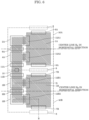
- FIG. 6 is a schematic plan view illustrating a layout configuration of pixels of solid-state imaging device 100 according to Embodiment 1.
- the plurality of pixels of imager 101 are two-dimensionally arranged in the imaging region on a semiconductor substrate, and pixel 50A included in the first pixel group and pixel 50B included in the second pixel group form a single pixel unit that is the smallest unit of distance measurement.
- FIG. 6 illustrates the layout configuration of a single pixel unit including pixels 50A and 50B having the circuit configuration illustrated in FIG. 2 .
- pixel 50A includes photoelectric converter 1A, readers 12A1 and 12A2, charge accumulators 2A and 4A, transfer controller 9A, outputter 11A, and exposure controllers 6A.
- Pixel 50B includes photoelectric converter 1B, readers 12B1 and 12B2, charge accumulators 3B and 5B, transfer controller 9B, outputter 11B, and exposure controllers 7B. Pixels 50A and 50B share FD 10 and overflow drain 8.
- Photoelectric converters 1A and 1B receive light reflected from object 600 and accumulate signal charge generated by photoelectric conversion.
- Charge accumulators 2A and 4A are respectively a first charge accumulator and a third charge accumulator which hold the signal charge accumulated in photoelectric converter 1A.
- Charge accumulators 2A and 4A are provided on an identical side of the outer edge of the region in which photoelectric converter 1A is formed.
- Charge accumulator 3B and 5B are respectively a second charge accumulator and a fourth charge accumulator which hold the signal charge accumulated in photoelectric converter 1B.
- Charge accumulators 3B and 5B are provided on an identical side of the outer edge of the region in which photoelectric converter 1B is formed.
- Readers 12A1 and 12A2 are respectively readers which read the signal charge from photoelectric converter 1A to charge accumulators 2A and 4A.
- Readers 12B1 and 12B2 are respectively readers which read the signal charge from photoelectric converter 1B to charge accumulators 3B and 5B.
- Transfer controller 9A is provided between charge accumulators 2A and 4A.
- Transfer controller 9B is provided between charge accumulators 3B and 5B.
- Outputter 11A is provided adjacent to charge accumulator 4A which is one of the two charge accumulators in pixel 50A.
- Outputter 11B is provided adjacent to charge accumulator 3B which is one of the two charge accumulators in pixel 50B.
- FD 10 is adjacent to charge accumulator 4A across outputter 11A and is adjacent to charge accumulator 3B across outputter 11B, and converts the signal charge into a voltage.
- Exposure controllers 6A are provided on two sides of photoelectric converter 1A that are orthogonal to the side thereof on which charge accumulators 2A and 4A are provided.
- Exposure controllers 7B are provided on two sides of photoelectric converter 1B that are orthogonal to the side thereof on which charge accumulators 3B and 5B are provided.
- Overflow drain 8 is provided adjacent to photoelectric converter 1A across exposure controller 6A or 7B and discharges, through exposure controller 6A or 7B, the signal charge accumulated in photoelectric converter 1A or 1B.
- Charge accumulators 2A, 4A, 3B, and 5B, readers 12A1, 12A2, 12B1, and 12B2, transfer controllers 9A and 9B, and outputters 11A and 11B are each formed by stacking a gate insulating film and a gate electrode above the semiconductor substrate.
- overflow drain 8 is desirably shared by adjacent pixels.
- FD 10 is connected to the source follower circuit, and amplifies and outputs a signal converted from a charge into a voltage; the configuration thereof is the same as or similar to a normal metal-oxide-semiconductor (MOS) image sensor, and thus description thereof will be omitted here.
- MOS metal-oxide-semiconductor
- the first pixel (pixel 50A) includes: a first reader and a second reader as the two readers; and a first exposure controller disposed on the same side as the first reader among the first reader and the second reader, and a second exposure controller disposed on the same side as the second reader among the first reader and the second reader, as the two exposure controllers
- the second pixel (pixel 50B) includes: a third reader and a fourth reader as the two readers; and a third exposure controller disposed on the same side as the third reader among the third reader and the fourth reader, and a fourth exposure controller disposed on the same side as the fourth reader among the third reader and the fourth reader, as the two exposure controllers.
- the gate electrode of reader 12A1 and the gate electrode of reader 12A2 are axisymmetrically arranged and are disposed on the identical side of the outer edge of a light-receiving region of photoelectric converter 1A. More specifically, in the present embodiment, in a plan view of the semiconductor substrate, the gate electrode of reader 12A1 and the gate electrode of reader 12A2 are arranged symmetrically with respect to center line H A passing through the center of the light-receiving region of photoelectric converter 1A, and are disposed on the identical side of the outer edge of the light-receiving region.
- the two gate electrodes of exposure controllers 6A are axisymmetrically arranged and are disposed on two sides of the outer edge of the light-receiving region of photoelectric converter 1A that are orthogonal to said identical side thereof.
- the gate electrode of one (the first exposure controller) of exposure controllers 6A is disposed on the same side as reader 12A1 among reader 12A1 (the first reader) and reader 12A2 (the second reader), and the gate electrode of the other (the second exposure controller) of exposure controllers 6A is disposed on the same side as reader 12A2 among reader 12A1 and reader 12A2.
- the two gate electrodes of exposure controllers 6A are respectively disposed on two sides that are close to reader 12A1 and reader 12A2 and orthogonal to the abovementioned identical side, and are arranged symmetrically with respect to center line H A .
- the gate electrode of reader 12B1 and the gate electrode of reader 12B2 are axisymmetrically arranged and are disposed on the identical side of the outer edge of a light-receiving region of photoelectric converter 1B. More specifically, in the present embodiment, in the abovementioned plan view, the gate electrode of reader 12B1 and the gate electrode of reader 12B2 are arranged symmetrically with respect to center line H B passing through the center of the light-receiving region of photoelectric converter 1B, and are disposed on the identical side of the outer edge of the light-receiving region.
- the two gate electrodes of exposure controllers 7B are axisymmetrically arranged and are disposed on two sides of the outer edge of the light-receiving region of photoelectric converter 1B that are orthogonal to said identical side thereof.
- the gate electrode of one (the third exposure controller) of exposure controllers 7B is disposed on the same side as reader 12B1 among reader 12B1 (the third reader) and reader 12B2 (the fourth reader), and the gate electrode of the other (the fourth exposure controller) of exposure controllers 7B is disposed on the same side as reader 12B2 among reader 12B1 and reader 12B2.
- the two gate electrodes of exposure controllers 7B are respectively disposed on two sides that are close to reader 12B1 and reader 12B2 and orthogonal to the abovementioned identical side, and are arranged symmetrically with respect to center line H B . The reason for this will be described below.
- the gate electrodes of the readers are not provided symmetrically, when leakage signals are generated due to background light or the like, the signals are not evenly distributed and are read at different rates. This leads to an error in the value obtained after subtraction of the background light in distance calculation, resulting in a decrease in the distance measurement accuracy.
- the gates of the readers are arranged symmetrically so that the amount of leakage signals due to background light or the like is equalized.
- FIG. 7 illustrates a distribution of potentials in the photoelectric converter and surrounding parts thereof according to Embodiment 1.
- FIG. 7 illustrates the distribution of potentials in the A-B cross-section in FIG. 6 .
- ODG ON
- the entire signal charge generated by light entry is desirably discharged to overflow drain 8.
- a small portion of the charge moves toward the gate of the reader under the influence of the potential distribution formed in the photoelectric conversion region.
- the gate electrodes of readers 12A1 and 12A2 are arranged symmetrically with respect to center line H A of photoelectric converter 1A in the horizontal direction, and two gate electrodes of exposure controllers 6A are respectively provided close to the gate electrodes of readers 12A1 and 12A2.
- the potential under the gate of the exposure controller may be set lower than the potential under the gate of the reader (drive pulse signal TG).
- FIG. 8 illustrates a distribution of potentials in a photoelectric converter and surrounding parts thereof according to a variation of Embodiment 1.
- a potential gradient is formed in the horizontal direction in the photoelectric converter.
- FIG. 9 illustrates a distribution of potentials in the horizontal direction in the photoelectric converter and surrounding parts thereof according to Embodiment 1.
- FIG. 9 illustrates the distribution of potentials in the C-D cross-section in FIG. 6 ; the solid line represents the distribution of potentials in the present embodiment, and the dashed line represents the distribution of potentials in a conventional example.
- the potential of the photoelectric converter when drive pulse signal TG is at the low level, has a gradient that makes a deep part near the gate electrode of the reader. With this, as illustrated in (b) in FIG.
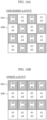
- FIG. 10A illustrates the layout of pixels arranged in a checkered pattern
- FIG. 10B illustrates the layout of pixels arranged in a stripe pattern.
- pixel 50A the first pixel
- pixel 50B the second pixel illustrated in FIG. 6 may be arranged in a checkered pattern or may be arranged in a stripe pattern.
- FIG. 11A illustrates the center of gravity of distance data in the layout of pixels arranged in a checkered pattern
- FIG. 11B illustrates the center of gravity of distance data in the layout of pixels arranged in a stripe pattern.
- the dashed line represents a range of calculation for signals for distance calculation that are output from the pixel unit made up of pixels 50A and 50B
- the black circle represents the center of gravity of distance data obtained by such calculation.
- the stripe layout illustrated in FIG. 10B is useful in an application in which only the horizontal resolution is considered important, whereas the checkered layout illustrated in FIG. 10A is preferred when both the horizontal and vertical resolutions are required. Furthermore, as illustrated in FIG. 11A , in the case of the checkered layout, since the centers of gravity of the distance data after the distance calculation are located in a checkered pattern, the vertical and horizontal resolutions aligned in the checkered pattern are substantially equal to the case where distance data is present for each pixel.
- the method of sharing FD 10 in the case of the checkered layout may be based on a sharing layout illustrated in FIG. 12 , for example.
- FIG. 12 illustrates an FD shared layout in the layout of the pixels arranged in the checkered pattern.
- the signals for distance calculation that are used in the distance data in the checkered pattern are output from the same FD amplifier. Therefore, the calculation can be performed without being affected by variations in sense capacitance between the pixels and variations in gain between amplifiers. Thus, it is possible to obtain high distance accuracy compared to the case where a distance is calculated using signals for distance calculation output from different FD amplifiers.
- FIG. 13 a configuration diagram of the gate wires of the exposure controller in an example of the checkered layout according to Embodiment 1.
- Drive pulse signals ODG1 and ODG2 are applied to the gate wires of the exposure controller, and therefore when there is a delay on the gate wires, the distance after calculation changes within an imaging surface, resulting in a decrease in accuracy. Furthermore, when the falling edges and the rising edges of drive pulse signals ODG1 and ODG2 are delayed, it is difficult to read the signal charge.
- the gate wires of the exposure controller are desirably arranged parallel to the short side of the imaging region and are further desirably supplied with the drive pulse signals from both ends of the gate wires.
- DC bias may be superimposed on drive pulse signals ODG1 and ODG2 that are applied to the gate of the exposure controller which controls exposure time. This advantageous effect will be described below.
- FIG. 14A illustrates a delay of drive pulse signal ODG at an end of the imaging region according to Embodiment 1
- FIG. 14B illustrates a delay of drive pulse signal ODG at the center of the imaging region according to Embodiment 1.
- the reset level of drive pulse signal ODG needs to be low in voltage because a power supply voltage is 2.8 V for mobile use, etc., but sometimes becomes close to the power supply voltage.
- Vth is this reset level, as illustrated on the left side (no DC bias) in FIG. 14A and FIG. 14B , when Vth is high, there is a difference in duty between an exposure ON period and an exposure OFF period, and the roundness of the waveform causes a misalignment in duty between the end and the center of the imaging region.
- there is an overlap between two exposure OFF periods determined by two drive pulse signals ODG1 and ODG2 and thus the resultant value after the calculation is different between the center and the end even when the distance to the subject is the same.
- the exposure ON period is separated at the end, and thus the distance calculation cannot be performed at the end.
- DC bias is applied to drive pulse signals ODG1 and ODG2 so that Vth is located at the amplification center of the pulse width. Accordingly, the duty can be 1:1 both at the end and at the center of the imaging region, and thus the in-plane distance measurement accuracy can be improved.
- Vth adjustment it is possible to obtain the same advantageous effects as the DC bias by making the impurity concentration of the exposure controller different from the impurity concentration of the reader so that the potential of the exposure controller becomes higher than the potential of the reader.
- Vth is desirably 50% of the amplitude of drive pulse signals ODG1 and ODG2.
- FIG. 15 is a timing chart illustrating a method for driving a solid-state imaging device according to Example 2.
- FIG. 16 is a schematic plan view of the imaging region for explaining that a different exposure control is performed for each pixel row in the solid-state imaging device according to Example 2.
- Example 2 in order to cope with a wide range of the reflectance of objects 600, the number of times drive pulse signal ODG is applied to the gate of the exposure controller is changed for each column, and thus exposure control is performed in such a way that the charge accumulator is not saturated even when object 600 having high reflectance is present.
- the number of times of exposure is different between drive pulse signal ODG1 (2j) in the 2j-th row and drive pulse signal ODG1 (2j+1) in the 2j+1-th row, and the number of times of exposure is different between drive pulse signal ODG2 (2j) in the 2j-th row and drive pulse signal ODG2 (2j+1) in the 2j+1-th row.
- FIG. 16 illustrates the case where the exposure controllers are wired in the direction of the short side (in this figure, the vertical direction); in this case, the number of times of exposure is different on a per-column basis.
- FIG. 17 is a timing chart illustrating a method for driving a solid-state imaging device according to a variation of Embodiment 2.
- the number of times of exposure for drive pulse signals OG1 and ODG2 is the same in the imaging region in the timing chart in FIG. 17 , the number of times the readers read drive pulse signals TG1 to TG4 may be controlled. Note that in Example 2, since the gate wires of the reader extend in the lateral direction, the amount of signals that are actually read to the charge accumulator can be adjusted on a per-row basis.
- the exposure periods are partially removed desirably at equal intervals, throughout all the exposure periods, in a pixel row or column in which the number of times of exposure is small, compared to the case where the exposure is performed more on the first half of the exposure after the start, for example, because simultaneity can be maintained.
- FIG. 18 is a schematic plan view illustrating a layout configuration of pixels of the solid-state imaging device according to Example 3.
- the solid-state imaging device according to the present embodiment is different from solid-state imaging device 100 according to Embodiment 1 only in that light-shielding films 20A and 20B are formed in the imaging region.
- light-shielding film 20A is provided so as to cover charge accumulators 2A and 4A and transfer controller 9A
- light-shielding film 20B is provided so as to cover charge accumulators 3B and 5B and transfer controller 9B.
- light-shielding films 20A and 20B are disposed so as to cover the charge accumulator and the gate electrode of the transfer controller. Meanwhile, the light-shielding film is selectively not disposed on the gate electrode of the exposure controller. With this, it is possible to reduce the increase in the parasitic capacitance of the exposure controller which is required to be driven at high speed.
- the light-shielding properties of the charge accumulator and the transfer controller improve, and thus the light resistance can be improved, and furthermore, the background light component is suppressed; thus, the distance accuracy can be improved.
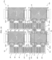
- FIG. 19 is a schematic plan view illustrating a layout configuration of pixels of the solid-state imaging device according to Embodiment 4
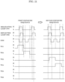
- FIG. 20 is a drive timing chart illustrating operations of the solid-state imaging device according to Example 4 during exposure.
- the solid-state imaging device includes a color filter, and as illustrated in FIG. 19 , has an RGB-IR array to enable both color imaging and distance measurement using IR pixels.
- the solid-state imaging device according to the present embodiment obtains four signals for distance calculation by using readers 12IR1 to 12IR4 on both sides of photoelectric converter 1IR of a pixel 50ir for IR reception (a third pixel). It is advantageous that the four signals for distance calculation can be obtained by sequentially switching drive pulse signals TG1 to TG4 to the high level in one period of irradiating light (PT), as illustrated in FIG. 20 .
- the number of light emission pulses can be reduced, and thus it is also advantageous that power consumption can be reduced.
- the exposure is controlled by readers 12IR1 to 12IR4, there is a need for four fast drive pulse signals TG1 to TG4. Therefore, a large wiring width is required, and a driver included in the solid-state imaging device is large in scale.
- FIG. 21 is a drive timing chart illustrating operations of a solid-state imaging device according to Variation 1 of Embodiment 4 during exposure.
- drive pulse signals TG1 and TG3 or drive pulse signals TG2 and TG4 are switched to the high level in one period of irradiating light (PT), and thus two signals for distance calculation are obtained.
- Readers 12IR1 to 12IR4 do not control exposure, but only read the signal controlled by drive pulse signal ODG in exposure controller 7IR. Note that the exposure sequence is divided into two while drive pulse signal ODG may be one.
- a signal for distance calculation is read by drive pulse signals TG1 and TG3
- the exposure timing for drive pulse signal ODG is delayed by the pulse width of irradiating light (PT)
- the signal for distance calculation is read by drive pulse signals TG2 and TG4 according to the charge accumulation state.
- a drive pulse signal having the same pulse width as an irradiating pulse is ODG only, and thus, compared to the embodiments illustrated in FIG. 19 and FIG. 20 , the pulse width of TG1 to TG4 is twice, and since the TG pulse does not control the exposure, the allowable amount of delay is large.
- the wiring width for TG1 to TG4 can be small and the scale of the driver can also be small.
- signals are read using readers 12IR1, 12IR3, 12R1, 12R2, 121, 12G2, 12B1, and 12B2.
- the present structure uses two readers for obtaining two signals having different exposure periods in the reading of all the pixels, it is also possible to use a configuration in which the RGB pixels have readers 12R1, 12G1, and 12B1 only, in the case where only one signal is obtained.
- FIG. 22A is a schematic plan view illustrating a layout configuration of pixels of a solid-state imaging device according to Variation 2 of Embodiment 4
- FIG. 22B is a drive timing chart illustrating operations of the solid-state imaging device according to variation 2 of Embodiment 4 during exposure.
- A0 and A2 may be obtained in the first exposure sequence
- A1 and A3 may be obtained in the second exposure sequence, as illustrated in FIG. 22B .
- FIG. 23 illustrates a distribution of potentials in the horizontal direction in the photoelectric converter and surrounding parts thereof according to Example 4. This does not apply to Variation 2 of Example 4.
- FIG. 23 illustrates the distribution of potentials in the E-F cross-section in FIG. 19 ; the solid line represents the distribution of potentials in the present embodiment, and the dashed line represents the distribution of potentials in a conventional example. This is different from that described in Embodiment 1 with reference to FIG. 9 in that, since the gate electrode of the reader is disposed on both sides of the photoelectric converter, the potential near the gate electrode on the both sides is flat so that charge can be transferred in both directions. With this, as illustrated in (b) in FIG.
- FD 10A is shared by two pixels 50r (a fifth pixel) and 50ir (the third pixel) and FD 10B is shared by two pixels 50g (a sixth pixel) and 50b (a fourth pixel), but one FD may be shared by these four pixels.
- the number of charge accumulators to which different drive pulse signals are applied increases by two, but it is possible to improve the distance measurement accuracy because there is no variation in sense capacitance.
- FIG. 24 illustrates a variation of the layout of pixels of the solid-state imaging device according to Example 4.
- the arrangement configuration of a pixel circuit according to the present embodiment can be applied to a 4 ⁇ 4 RGB-IR array such as that illustrated in this figure.
- the IR pixels are arranged in a checkered pattern, and thus it is advantageous that the resolution in both the horizontal direction and the vertical direction is twice as high as that of a 2 ⁇ 2 array such as that illustrated in FIG. 19 .
- the TOF operation using four charge accumulators is possible even in the RGB-IR array, and thus both the distance measurement range and the distance measurement accuracy can be sufficient, and it is possible to obtain an RGB-IR image as well.
- Example 5 A solid-state imaging device and a method for driving the same according to Example 5, not covered by the appended claims, will be described, focusing on differences from Embodiment 1 and Examples 2-4.
- FIG. 25 is a drive timing chart illustrating operations of the solid-state imaging device according to Example 5 during exposure. Unlike the driving method illustrated in FIG. 3 according to Embodiment 1, in the present embodiment, as illustrated in FIG. 25 , signal charge for one frame is read once after the first exposure sequence, then, after the second exposure sequence is performed, one frame is read, and lastly the same signals for the two frames are added up. Note that the configuration illustrated in FIG. 6 according to Embodiment 1 is assumed as the layout configuration of pixels of the solid-state imaging device according to the present embodiment.
- drive pulse signal TG3 is applied to the gate electrode of reader 12IR3 with the same timing as when drive pulse signal TG1 is applied to the gate electrode of reader 12IR1 in the first exposure sequence, and drive pulse signal TG1 is applied with the same timing as when drive pulse signal TG3 is applied in the first exposure sequence.
- drive pulse signal TG4 is applied to the gate electrode of reader 12IR4 with the same timing as when drive pulse signal TG2 is applied to the gate electrode of reader 12IR2 in the first exposure sequence, and drive pulse signal TG2 is applied with the same timing as when drive pulse signal TG4 is applied in the first exposure sequence.
- an embedded channel capacitive coupling element is used as the charge accumulator.
- dark current is generated, which may be different in each charge accumulator.
- the calculation result is affected, and thus dark current components needs to be the same for those that are subtracted from each other in the calculation.
- the present driving method it is possible to solve this problem by interchanging the timing at which drive pulse signal TG for reading is applied in the second exposure sequence.
- SD(A) represents the dark current in the first charge accumulator
- SD(B) represents the dark current in the third charge accumulator
- SD(C) represents the dark current in the second charge accumulator
- SD(D) represents the dark current in the fourth charge accumulator.
- signals that are accumulated in the respective charge accumulators and read after the first exposure is completed are A0+SD(A), A2+SD(B), A1+SD(C), and A3+SD(D).
- signals that are accumulated in the respective charge accumulators and read after the second exposure is completed are A2+SD(A), A0+SD(B), A3+SD(C), and A1+SD(D). Adding up these for the same signals for distance calculation results in the following.
- Either A0 or A2 is a signal having distance information, and one of A0 and A2 is a signal for background light information (BG); the same applies to A1 and 3.
- a method for calculating a distance using these four signals is as described in Embodiment 1.
- the timing for applying drive pulse signal TG is changed for different frames, and addition thereof allows the dark current in the signal having the distance information and the dark current in the corresponding BG signal to match each other; thus, even when there is a difference in dark current between the charge accumulators in a pixel, these can be cancelled.
- errors in distance measurement include (1) a difference in the number of sensitive electrons between pixels that is caused by production tolerance of on-chip lenses, aperture dimension, etc., and (2) a difference in amplifier gain that is caused by a difference in sense capacitance, etc.
- the abovementioned (2) can be solved, but the abovementioned (1) remains. This does not stand out in video because of variations in distance measurement that are caused by shot noise, but may become problematic when a shot noise reduction approach is used.
- the solid-state imaging device is small and enables three-dimensional measurement with high distance measurement accuracy and a wide distance measurement range, and is useful, for example, for three-dimensional measurement of persons, buildings, etc.
Landscapes
- Engineering & Computer Science (AREA)
- Physics & Mathematics (AREA)
- Radar, Positioning & Navigation (AREA)
- Computer Networks & Wireless Communication (AREA)
- General Physics & Mathematics (AREA)
- Remote Sensing (AREA)
- Electromagnetism (AREA)
- Signal Processing (AREA)
- Multimedia (AREA)
- Solid State Image Pick-Up Elements (AREA)
- Transforming Light Signals Into Electric Signals (AREA)
- Optical Radar Systems And Details Thereof (AREA)
- Studio Devices (AREA)
Claims (17)
- Dispositif d'imagerie à semi-conducteurs comprenant une pluralité de pixels agencés dans une matrice sur un substrat semi-conducteur,
dans lequel chacun de la pluralité de pixels (50A) comporte :un convertisseur photoélectrique (1A) qui est configuré pour recevoir une lumière d'un objet et convertir la lumière en charge ;un drain de débordement (8) qui est configuré pour décharger la charge du convertisseur photoélectrique (1A) ;deux contrôleurs d'exposition (6A) qui sont configurés pour commuter entre l'accumulation de la charge dans le convertisseur photoélectrique (1A) et la décharge de la charge du convertisseur photoélectrique (1A), chacun des contrôleurs d'exposition (6A) ayant une grille à laquelle est appliqué un signal d'impulsion de commande (ODG1) pour contrôler qu'une charge de signal générée dans le convertisseur photoélectrique (1A) est soit déchargée vers le drain de débordement (8) via les contrôleurs d'exposition (6A) et ne s'accumule pas dans le convertisseur photoélectrique (1A), soit non déchargée vers le drain de débordement (8) et s'accumule dans le convertisseur photoélectrique (1A) ;deux accumulateurs de charge (2A, 4A) dont chacun est configuré pour retenir la charge de signal accumulée dans le convertisseur photoélectrique (1A) ;deux lecteurs (12A1, 12A2) qui sont configurés pour lire respectivement la charge de signal du convertisseur photoélectrique (1A) vers les deux accumulateurs de charge (2A, 4A) et obtenir deux signaux ayant des périodes d'exposition différentes ;un contrôleur de transfert (9A) qui effectue un contrôle de transfert, notamment en contrôlant si la charge accumulée dans l'un des deux accumulateurs de charge (2A, 4A) est transférée ou bloquée pour être transférée vers l'autre des deux accumulateurs de charge, etdans lequelle contrôleur de transfert (9A) est disposé entre les deux accumulateurs de charge (2A, 4A),chacun des deux contrôleurs d'exposition (6A) et des deux lecteurs (12A1, 12A2) a une électrode de grille formée sur le substrat semi-conducteur, etdans une vue en plan du substrat semi-conducteur, une électrode de grille de l'un des deux lecteurs (12A1, 12A2) et une électrode de grille de l'autre des deux lecteurs (12A1, 12A2) sont agencées asymétriquement par rapport à une ligne centrale (HA) passant par le centre d'une région de réception de lumière du convertisseur photoélectrique (1A) et sont disposées du même côté d'un bord extérieur d'une région de réception de lumière du convertisseur photoélectrique (1A), et les deux électrodes de grille des contrôleurs d'exposition (6A) sont agencées asymétriquement par rapport à ladite ligne centrale (HA) et sont disposées des deux côtés du bord extérieur de la région de réception de lumière de convertisseur photoélectrique (1A) qui sont orthogonaux audit même côté du bord extérieur de la région de réception de lumière de convertisseur photoélectrique (1A). - Dispositif d'imagerie à semi-conducteurs selon la revendication 1,dans lequel le contrôleur de transfert (9A) est disposé entre les deux accumulateurs de charge (2A, 4A) dans une direction verticale, etles deux lecteurs (12A1, 12A2) sont disposés entre le convertisseur photoélectrique (1A) et les deux accumulateurs de charge (2A, 4A), respectivement, dans un direction horizontale.
- Dispositif d'imagerie à semi-conducteurs selon la revendication 1 ou 2,
dans lequel le contrôleur de transfert (9A) a une électrode de grille réglée sur un potentiel de référence commun. - Dispositif d'imagerie à semi-conducteurs selon la revendication 1,dans lequel chacun de la pluralité de pixels (50A, 50B) comporte en outreun film de protection contre la lumière (20A, 20B) qui protège au moins une partie d'une électrode de grille de chacun des deux accumulateurs de charge (2A, 4A, 3B, 5B) de la lumière et évite de protéger une électrode de grille du contrôleur d'exposition (6A, 7B) de la lumière.
- Dispositif d'imagerie à semi-conducteurs selon la revendication 4, comprenant en outre
un contrôleur de commande qui contrôle la commande d'un signal d'impulsion de commande qui est appliqué à une électrode de grille de chacun des contrôleurs d'exposition (6A, 7B) et à une électrode de grille de chacun des deux lecteurs (12A1, 12A2, 12B1, 12B2). - Dispositif d'imagerie à semi-conducteurs selon la revendication 5, comprenant en outreune pluralité de fils de grille de contrôle d'exposition qui sont fournis pour chaque rangée de pixels ou chaque colonne de pixels et par lesquels le signal d'impulsion de commande est transmis à l'électrode de grille du contrôleur d'exposition (6A, 7B),dans lequel la pluralité de fils de grille de contrôle d'exposition sont disposés parallèlement à un côté court d'une région d'imagerie sur le substrat semi-conducteur, la région d'imagerie étant une région dans laquelle la pluralité de pixels sont agencés.
- Dispositif d'imagerie à semi-conducteurs selon la revendication 5 ou 6, comprenant en outreun fil de grille de lecture à travers lequel le signal d'impulsion de commande est transmis à l'électrode de grille de chacun des deux lecteurs (12A1, 12A2),dans lequel le nombre total de fois où le fil de grille de lecture passe à un niveau haut est différent sur une pluralité de fils de grille de lecture.
- Dispositif d'imagerie à semi-conducteurs selon l'une quelconque des revendications 5 à 7, comprenant en outreun fil de grille de contrôle d'exposition à travers lequel le signal d'impulsion de commande est transmis du contrôleur de commande à l'électrode de grille de chacun des contrôleurs d'exposition (6A, 7B),dans lequel le nombre total de fois où le fil de grille de contrôle d'exposition passe à un niveau bas est différent sur une pluralité de fils de grille de contrôle d'exposition.
- Dispositif d'imagerie à semi-conducteurs selon l'une quelconque des revendications 5 à 8,
dans lequel une tension de polarisation à courant continu (CC) est superposée sur le signal d'impulsion de commande. - Dispositif d'imagerie à semi-conducteurs selon l'une quelconque des revendications 1 à 9,dans lequel la pluralité de pixels comportent au moins un premier pixel (50A) et un deuxième pixel (50B) qui reçoivent une lumière infrarouge, etle premier pixel et le deuxième pixel partagent une diffusion flottante (10) qui convertit la charge des deux accumulateurs de charge (2A, 4A, 3B, 5B) en une tension.
- Dispositif d'imagerie à semi-conducteurs selon la revendication 10,dans lequel un signal d'impulsion de commande (VG1) est appliqué à un accumulateur de charge (2A) disposé plus loin de la diffusion flottante (10) parmi les deux accumulateurs de charge (2A, 4A) qui sont inclus dans le premier pixel (50A), et un signal d'impulsion de commande (VG4) est appliqué à un accumulateur de charge (5B) disposé plus loin de la diffusion flottante (10) parmi les deux accumulateurs de charge (3B, 5B) qui sont inclus dans le deuxième pixel (50B),et dans lequel les deux signaux d'impulsion de commande (VG1, VG4) ont le même comportement.
- Dispositif d'imagerie à semi-conducteurs selon la revendication 10 ou 11,dans lequel la pluralité de pixels comporte une pluralité de premiers pixels et une pluralité de deuxièmes pixels, etdans une vue en plan du substrat semi-conducteur, les premiers pixels et les deuxièmes pixels sont agencés en damier, etla diffusion flottante est agencée en damier dans la vue en plan.
- Dispositif d'imagerie à semi-conducteurs selon la revendication 10 ou 11,dans lequel la pluralité de pixels comporte une pluralité de premiers pixels et une pluralité de deuxièmes pixels, etdans une vue en plan du substrat semi-conducteur, les premiers pixels et les deuxièmes pixels sont agencés en bandes, etla diffusion flottante est agencée en bandes dans la vue en plan.
- Dispositif d'imagerie à semi-conducteurs selon la revendication 10,dans lequel la pluralité de pixels comportent un troisième pixel, un quatrième pixel, un cinquième pixel et un sixième pixel qui sont agencés de manière bidimensionnelle,le troisième pixel comporte :le convertisseur photoélectrique qui est unique ;les deux contrôleurs d'exposition ; etquatre lecteurs qui lisent la charge dans le convertisseur photoélectrique, etchacun du quatrième pixel, du cinquième pixel et du sixième pixel comporte :le convertisseur photoélectrique qui est unique ;les deux contrôleurs d'exposition ; etles deux lecteurs.
- Dispositif d'imagerie à semi-conducteurs selon la revendication 14,dans lequel chacun du troisième pixel, du cinquième pixel, et du sixième pixel comporte en outre les deux accumulateurs de charge, etle quatrième pixel comporteles deux accumulateurs de charge qui accumulent la charge lue dans le convertisseur photoélectrique du troisième pixel par deux lecteurs parmi les quatre lecteurs du troisième pixel, et la charge lue dans le convertisseur photoélectrique du quatrième pixel par les deux lecteurs du quatrième pixel.
- Dispositif d'imagerie à semi-conducteurs selon la revendication 14, comprenant en outreun contrôleur de commande qui contrôle la commande d'un signal d'impulsion de commande qui est appliqué à l'électrode de grille de chacun des deux contrôleurs d'exposition, des deux lecteurs, et des quatre lecteurs ;un mode de commande d'image dans lequel une image couleur est obtenue en utilisant les quatrième à sixième pixels ; etun mode de commande de mesure de distance dans lequel la lumière provenant de l'objet basée sur un faisceau pulsé émis vers l'objet est convertie en charge en utilisant le convertisseur photoélectrique du troisième pixel, et un signal de calcul de distance est obtenu en utilisant les accumulateurs de charge du troisième pixel et du quatrième pixel.
- Dispositif d'imagerie à semi-conducteurs selon l'une quelconque des revendications 15 à 16,
dans lequel les troisième à sixième pixels forment un groupe de pixels de quatre pixels de haut par quatre pixels large, et dans la vue en plan, le troisième pixel est agencé en damier dans le groupe de pixels.
Applications Claiming Priority (2)
| Application Number | Priority Date | Filing Date | Title |
|---|---|---|---|
| JP2015154552 | 2015-08-04 | ||
| PCT/JP2016/003493 WO2017022218A1 (fr) | 2015-08-04 | 2016-07-28 | Dispositif d'imagerie à semi-conducteurs |
Publications (3)
| Publication Number | Publication Date |
|---|---|
| EP3334152A1 EP3334152A1 (fr) | 2018-06-13 |
| EP3334152A4 EP3334152A4 (fr) | 2018-08-22 |
| EP3334152B1 true EP3334152B1 (fr) | 2023-10-11 |
Family
ID=57942686
Family Applications (1)
| Application Number | Title | Priority Date | Filing Date |
|---|---|---|---|
| EP16832501.7A Active EP3334152B1 (fr) | 2015-08-04 | 2016-07-28 | Dispositif d'imagerie à semi-conducteurs |
Country Status (5)
| Country | Link |
|---|---|
| US (1) | US10666875B2 (fr) |
| EP (1) | EP3334152B1 (fr) |
| JP (1) | JP6738334B2 (fr) |
| CN (1) | CN107925733B (fr) |
| WO (1) | WO2017022218A1 (fr) |
Families Citing this family (12)
| Publication number | Priority date | Publication date | Assignee | Title |
|---|---|---|---|---|
| CN108389870A (zh) | 2017-02-03 | 2018-08-10 | 松下知识产权经营株式会社 | 摄像装置 |
| JP6653482B2 (ja) * | 2017-04-06 | 2020-02-26 | パナソニックIpマネジメント株式会社 | 撮像装置、およびそれに用いられる固体撮像装置 |
| DE112018006100T5 (de) * | 2017-12-26 | 2020-10-29 | Robert Bosch Gmbh | Einzelchip-rgb-d-kamera |
| KR102488321B1 (ko) * | 2017-12-29 | 2023-01-13 | 삼성전자주식회사 | 3차원 이미지 센서의 픽셀 어레이 및 3차원 이미지 센서의 구동 방법 |
| US11092678B2 (en) * | 2018-06-21 | 2021-08-17 | Analog Devices, Inc. | Measuring and removing the corruption of time-of-flight depth images due to internal scattering |
| KR102615195B1 (ko) * | 2018-07-19 | 2023-12-18 | 삼성전자주식회사 | ToF 기반의 3D 이미지 센서 및 그 이미지 센서를 구비한 전자 장치 |
| WO2020080065A1 (fr) * | 2018-10-16 | 2020-04-23 | 株式会社ブルックマンテクノロジ | Dispositif de mesure de distance, appareil de prise de vues et procédé de réglage de l'entraînement d'un dispositif de mesure de distance |
| WO2020166572A1 (fr) * | 2019-02-15 | 2020-08-20 | パナソニックセミコンダクターソリューションズ株式会社 | Dispositif d'imagerie et procédé de calcul d'informations de distance |
| WO2020195046A1 (fr) * | 2019-03-27 | 2020-10-01 | パナソニックIpマネジメント株式会社 | Dispositif d'imagerie à semi-conducteurs |
| CN110346780A (zh) * | 2019-07-31 | 2019-10-18 | 炬佑智能科技(苏州)有限公司 | 飞行时间传感相机及其局部检测精度调整方法 |
| CN110456380B (zh) * | 2019-07-31 | 2021-12-28 | 炬佑智能科技(苏州)有限公司 | 飞行时间传感相机及其深度检测方法 |
| JP7505221B2 (ja) * | 2020-03-25 | 2024-06-25 | Toppanホールディングス株式会社 | 固体撮像素子および撮像システム |
Citations (2)
| Publication number | Priority date | Publication date | Assignee | Title |
|---|---|---|---|---|
| WO2007119626A1 (fr) * | 2006-03-31 | 2007-10-25 | National University Corporation Shizuoka University | Element semiconducteur de mesure de distance et element a solide de formation d'image |
| US20120248290A1 (en) * | 2011-03-31 | 2012-10-04 | Honda Motor Co., Ltd. | Solid-state image sensing device |
Family Cites Families (9)
| Publication number | Priority date | Publication date | Assignee | Title |
|---|---|---|---|---|
| JP4235729B2 (ja) | 2003-02-03 | 2009-03-11 | 国立大学法人静岡大学 | 距離画像センサ |
| JP4524609B2 (ja) * | 2004-10-29 | 2010-08-18 | ソニー株式会社 | 固体撮像素子、固体撮像素子の駆動方法および撮像装置 |
| TWI433307B (zh) * | 2008-10-22 | 2014-04-01 | Sony Corp | 固態影像感測器、其驅動方法、成像裝置及電子器件 |
| JP2010161183A (ja) * | 2009-01-07 | 2010-07-22 | Panasonic Corp | 固体撮像装置 |
| JP5404112B2 (ja) | 2009-03-12 | 2014-01-29 | キヤノン株式会社 | 固体撮像素子、その駆動方法及び撮像システム |
| US8179463B1 (en) * | 2009-05-19 | 2012-05-15 | On Semiconductor Trading Ltd. | Image sensor with shared node |
| WO2014002415A1 (fr) * | 2012-06-28 | 2014-01-03 | パナソニック株式会社 | Dispositif d'imagerie |
| JP6442710B2 (ja) * | 2013-07-23 | 2018-12-26 | パナソニックIpマネジメント株式会社 | 固体撮像装置、撮像装置及びその駆動方法 |
| WO2015025497A1 (fr) * | 2013-08-23 | 2015-02-26 | パナソニックIpマネジメント株式会社 | Système de mesure de la distance et dispositif de génération de signaux |
-
2016
- 2016-07-28 WO PCT/JP2016/003493 patent/WO2017022218A1/fr not_active Ceased
- 2016-07-28 JP JP2017532369A patent/JP6738334B2/ja active Active
- 2016-07-28 CN CN201680045328.2A patent/CN107925733B/zh active Active
- 2016-07-28 EP EP16832501.7A patent/EP3334152B1/fr active Active
-
2018
- 2018-01-29 US US15/882,316 patent/US10666875B2/en active Active
Patent Citations (4)
| Publication number | Priority date | Publication date | Assignee | Title |
|---|---|---|---|---|
| WO2007119626A1 (fr) * | 2006-03-31 | 2007-10-25 | National University Corporation Shizuoka University | Element semiconducteur de mesure de distance et element a solide de formation d'image |
| US20090114919A1 (en) * | 2006-03-31 | 2009-05-07 | National University Corporation Shizuoka Univ. | Semiconductor range-finding element and solid-state imaging device |
| US20120248290A1 (en) * | 2011-03-31 | 2012-10-04 | Honda Motor Co., Ltd. | Solid-state image sensing device |
| JP2012217060A (ja) * | 2011-03-31 | 2012-11-08 | Honda Motor Co Ltd | 固体撮像装置 |
Also Published As
| Publication number | Publication date |
|---|---|
| EP3334152A4 (fr) | 2018-08-22 |
| JP6738334B2 (ja) | 2020-08-12 |
| WO2017022218A1 (fr) | 2017-02-09 |
| US10666875B2 (en) | 2020-05-26 |
| EP3334152A1 (fr) | 2018-06-13 |
| CN107925733A (zh) | 2018-04-17 |
| CN107925733B (zh) | 2020-09-18 |
| JPWO2017022218A1 (ja) | 2018-05-24 |
| US20180167562A1 (en) | 2018-06-14 |
Similar Documents
| Publication | Publication Date | Title |
|---|---|---|
| EP3334152B1 (fr) | Dispositif d'imagerie à semi-conducteurs | |
| EP3333893B1 (fr) | Dispositif d'imagerie à semi-conducteurs | |
| CN107852470B (zh) | 固体摄像装置的驱动方法 | |
| US10838066B2 (en) | Solid-state imaging device, distance measurement device, and distance measurement method | |
| KR101508410B1 (ko) | 거리 화상 센서, 및 촬상 신호를 비행시간법에 의해 생성하는 방법 | |
| JP6145826B2 (ja) | 撮像装置及びその駆動方法 | |
| US11399148B2 (en) | Solid-state imaging device and imaging apparatus including same | |
| US10491842B2 (en) | Imaging device, a solid-state imaging device for use in the imaging device | |
| US20130228691A1 (en) | Circuit configuration and method for time of flight sensor | |
| JP2011128024A (ja) | 3次元撮像装置 | |
| US10048380B2 (en) | Distance-measuring imaging device and solid state imaging element | |
| JPWO2016133053A1 (ja) | 距離画像計測装置 | |
| US11194025B2 (en) | Solid-state imaging device and imaging apparatus including same |
Legal Events
| Date | Code | Title | Description |
|---|---|---|---|
| STAA | Information on the status of an ep patent application or granted ep patent |
Free format text: STATUS: THE INTERNATIONAL PUBLICATION HAS BEEN MADE |
|
| PUAI | Public reference made under article 153(3) epc to a published international application that has entered the european phase |
Free format text: ORIGINAL CODE: 0009012 |
|
| STAA | Information on the status of an ep patent application or granted ep patent |
Free format text: STATUS: REQUEST FOR EXAMINATION WAS MADE |
|
| 17P | Request for examination filed |
Effective date: 20180125 |
|
| AK | Designated contracting states |
Kind code of ref document: A1 Designated state(s): AL AT BE BG CH CY CZ DE DK EE ES FI FR GB GR HR HU IE IS IT LI LT LU LV MC MK MT NL NO PL PT RO RS SE SI SK SM TR |
|
| AX | Request for extension of the european patent |
Extension state: BA ME |
|
| A4 | Supplementary search report drawn up and despatched |
Effective date: 20180720 |
|
| RIC1 | Information provided on ipc code assigned before grant |
Ipc: G01S 17/89 20060101ALI20180716BHEP Ipc: H04N 5/369 20110101ALI20180716BHEP Ipc: H01L 27/146 20060101ALI20180716BHEP Ipc: G01S 7/486 20060101AFI20180716BHEP |
|
| DAV | Request for validation of the european patent (deleted) | ||
| DAX | Request for extension of the european patent (deleted) | ||
| STAA | Information on the status of an ep patent application or granted ep patent |
Free format text: STATUS: EXAMINATION IS IN PROGRESS |
|
| 17Q | First examination report despatched |
Effective date: 20200511 |
|
| RAP1 | Party data changed (applicant data changed or rights of an application transferred) |
Owner name: PANASONIC SEMICONDUCTOR SOLUTIONS CO., LTD. |
|
| RAP3 | Party data changed (applicant data changed or rights of an application transferred) |
Owner name: NUVOTON TECHNOLOGY CORPORATION JAPAN |
|
| RAP3 | Party data changed (applicant data changed or rights of an application transferred) |
Owner name: NUVOTON TECHNOLOGY CORPORATION JAPAN |
|
| REG | Reference to a national code |
Ref country code: DE Ref legal event code: R079 Free format text: PREVIOUS MAIN CLASS: H04N0005369000 Ipc: H04N0025700000 Ref country code: DE Ref legal event code: R079 Ref document number: 602016083415 Country of ref document: DE Free format text: PREVIOUS MAIN CLASS: H04N0005369000 Ipc: H04N0025700000 |
|
| RIC1 | Information provided on ipc code assigned before grant |
Ipc: G01S 17/894 20200101ALI20230427BHEP Ipc: G01S 7/4863 20200101ALI20230427BHEP Ipc: G01S 7/481 20060101ALI20230427BHEP Ipc: H01L 27/146 20060101ALI20230427BHEP Ipc: H04N 25/70 20230101AFI20230427BHEP |
|
| GRAP | Despatch of communication of intention to grant a patent |
Free format text: ORIGINAL CODE: EPIDOSNIGR1 |
|
| STAA | Information on the status of an ep patent application or granted ep patent |
Free format text: STATUS: GRANT OF PATENT IS INTENDED |
|
| INTG | Intention to grant announced |
Effective date: 20230615 |
|
| GRAS | Grant fee paid |
Free format text: ORIGINAL CODE: EPIDOSNIGR3 |
|
| GRAA | (expected) grant |
Free format text: ORIGINAL CODE: 0009210 |
|
| STAA | Information on the status of an ep patent application or granted ep patent |
Free format text: STATUS: THE PATENT HAS BEEN GRANTED |
|
| AK | Designated contracting states |
Kind code of ref document: B1 Designated state(s): AL AT BE BG CH CY CZ DE DK EE ES FI FR GB GR HR HU IE IS IT LI LT LU LV MC MK MT NL NO PL PT RO RS SE SI SK SM TR |
|
| REG | Reference to a national code |
Ref country code: GB Ref legal event code: FG4D |
|
| REG | Reference to a national code |
Ref country code: CH Ref legal event code: EP |
|
| REG | Reference to a national code |
Ref country code: DE Ref legal event code: R096 Ref document number: 602016083415 Country of ref document: DE |
|
| P01 | Opt-out of the competence of the unified patent court (upc) registered |
Effective date: 20231004 |
|
| REG | Reference to a national code |
Ref country code: IE Ref legal event code: FG4D |
|
| REG | Reference to a national code |
Ref country code: LT Ref legal event code: MG9D |
|
| REG | Reference to a national code |
Ref country code: NL Ref legal event code: MP Effective date: 20231011 |
|
| REG | Reference to a national code |
Ref country code: AT Ref legal event code: MK05 Ref document number: 1621417 Country of ref document: AT Kind code of ref document: T Effective date: 20231011 |
|
| P03 | Opt-out of the competence of the unified patent court (upc) deleted | ||
| PG25 | Lapsed in a contracting state [announced via postgrant information from national office to epo] |
Ref country code: NL Free format text: LAPSE BECAUSE OF FAILURE TO SUBMIT A TRANSLATION OF THE DESCRIPTION OR TO PAY THE FEE WITHIN THE PRESCRIBED TIME-LIMIT Effective date: 20231011 |
|
| PG25 | Lapsed in a contracting state [announced via postgrant information from national office to epo] |
Ref country code: GR Free format text: LAPSE BECAUSE OF FAILURE TO SUBMIT A TRANSLATION OF THE DESCRIPTION OR TO PAY THE FEE WITHIN THE PRESCRIBED TIME-LIMIT Effective date: 20240112 |
|
| PG25 | Lapsed in a contracting state [announced via postgrant information from national office to epo] |
Ref country code: IS Free format text: LAPSE BECAUSE OF FAILURE TO SUBMIT A TRANSLATION OF THE DESCRIPTION OR TO PAY THE FEE WITHIN THE PRESCRIBED TIME-LIMIT Effective date: 20240211 |
|
| PG25 | Lapsed in a contracting state [announced via postgrant information from national office to epo] |
Ref country code: LT Free format text: LAPSE BECAUSE OF FAILURE TO SUBMIT A TRANSLATION OF THE DESCRIPTION OR TO PAY THE FEE WITHIN THE PRESCRIBED TIME-LIMIT Effective date: 20231011 |
|
| PG25 | Lapsed in a contracting state [announced via postgrant information from national office to epo] |
Ref country code: AT Free format text: LAPSE BECAUSE OF FAILURE TO SUBMIT A TRANSLATION OF THE DESCRIPTION OR TO PAY THE FEE WITHIN THE PRESCRIBED TIME-LIMIT Effective date: 20231011 |
|
| PG25 | Lapsed in a contracting state [announced via postgrant information from national office to epo] |
Ref country code: ES Free format text: LAPSE BECAUSE OF FAILURE TO SUBMIT A TRANSLATION OF THE DESCRIPTION OR TO PAY THE FEE WITHIN THE PRESCRIBED TIME-LIMIT Effective date: 20231011 |
|
| PG25 | Lapsed in a contracting state [announced via postgrant information from national office to epo] |
Ref country code: LT Free format text: LAPSE BECAUSE OF FAILURE TO SUBMIT A TRANSLATION OF THE DESCRIPTION OR TO PAY THE FEE WITHIN THE PRESCRIBED TIME-LIMIT Effective date: 20231011 Ref country code: IS Free format text: LAPSE BECAUSE OF FAILURE TO SUBMIT A TRANSLATION OF THE DESCRIPTION OR TO PAY THE FEE WITHIN THE PRESCRIBED TIME-LIMIT Effective date: 20240211 Ref country code: GR Free format text: LAPSE BECAUSE OF FAILURE TO SUBMIT A TRANSLATION OF THE DESCRIPTION OR TO PAY THE FEE WITHIN THE PRESCRIBED TIME-LIMIT Effective date: 20240112 Ref country code: ES Free format text: LAPSE BECAUSE OF FAILURE TO SUBMIT A TRANSLATION OF THE DESCRIPTION OR TO PAY THE FEE WITHIN THE PRESCRIBED TIME-LIMIT Effective date: 20231011 Ref country code: BG Free format text: LAPSE BECAUSE OF FAILURE TO SUBMIT A TRANSLATION OF THE DESCRIPTION OR TO PAY THE FEE WITHIN THE PRESCRIBED TIME-LIMIT Effective date: 20240111 Ref country code: AT Free format text: LAPSE BECAUSE OF FAILURE TO SUBMIT A TRANSLATION OF THE DESCRIPTION OR TO PAY THE FEE WITHIN THE PRESCRIBED TIME-LIMIT Effective date: 20231011 Ref country code: PT Free format text: LAPSE BECAUSE OF FAILURE TO SUBMIT A TRANSLATION OF THE DESCRIPTION OR TO PAY THE FEE WITHIN THE PRESCRIBED TIME-LIMIT Effective date: 20240212 |
|
| PG25 | Lapsed in a contracting state [announced via postgrant information from national office to epo] |
Ref country code: SE Free format text: LAPSE BECAUSE OF FAILURE TO SUBMIT A TRANSLATION OF THE DESCRIPTION OR TO PAY THE FEE WITHIN THE PRESCRIBED TIME-LIMIT Effective date: 20231011 Ref country code: RS Free format text: LAPSE BECAUSE OF FAILURE TO SUBMIT A TRANSLATION OF THE DESCRIPTION OR TO PAY THE FEE WITHIN THE PRESCRIBED TIME-LIMIT Effective date: 20231011 Ref country code: PL Free format text: LAPSE BECAUSE OF FAILURE TO SUBMIT A TRANSLATION OF THE DESCRIPTION OR TO PAY THE FEE WITHIN THE PRESCRIBED TIME-LIMIT Effective date: 20231011 Ref country code: NO Free format text: LAPSE BECAUSE OF FAILURE TO SUBMIT A TRANSLATION OF THE DESCRIPTION OR TO PAY THE FEE WITHIN THE PRESCRIBED TIME-LIMIT Effective date: 20240111 Ref country code: LV Free format text: LAPSE BECAUSE OF FAILURE TO SUBMIT A TRANSLATION OF THE DESCRIPTION OR TO PAY THE FEE WITHIN THE PRESCRIBED TIME-LIMIT Effective date: 20231011 Ref country code: HR Free format text: LAPSE BECAUSE OF FAILURE TO SUBMIT A TRANSLATION OF THE DESCRIPTION OR TO PAY THE FEE WITHIN THE PRESCRIBED TIME-LIMIT Effective date: 20231011 |
|
| PG25 | Lapsed in a contracting state [announced via postgrant information from national office to epo] |
Ref country code: DK Free format text: LAPSE BECAUSE OF FAILURE TO SUBMIT A TRANSLATION OF THE DESCRIPTION OR TO PAY THE FEE WITHIN THE PRESCRIBED TIME-LIMIT Effective date: 20231011 |
|
| REG | Reference to a national code |
Ref country code: DE Ref legal event code: R097 Ref document number: 602016083415 Country of ref document: DE |
|
| PG25 | Lapsed in a contracting state [announced via postgrant information from national office to epo] |
Ref country code: CZ Free format text: LAPSE BECAUSE OF FAILURE TO SUBMIT A TRANSLATION OF THE DESCRIPTION OR TO PAY THE FEE WITHIN THE PRESCRIBED TIME-LIMIT Effective date: 20231011 |
|
| PG25 | Lapsed in a contracting state [announced via postgrant information from national office to epo] |
Ref country code: SK Free format text: LAPSE BECAUSE OF FAILURE TO SUBMIT A TRANSLATION OF THE DESCRIPTION OR TO PAY THE FEE WITHIN THE PRESCRIBED TIME-LIMIT Effective date: 20231011 |
|
| PG25 | Lapsed in a contracting state [announced via postgrant information from national office to epo] |
Ref country code: SM Free format text: LAPSE BECAUSE OF FAILURE TO SUBMIT A TRANSLATION OF THE DESCRIPTION OR TO PAY THE FEE WITHIN THE PRESCRIBED TIME-LIMIT Effective date: 20231011 Ref country code: SK Free format text: LAPSE BECAUSE OF FAILURE TO SUBMIT A TRANSLATION OF THE DESCRIPTION OR TO PAY THE FEE WITHIN THE PRESCRIBED TIME-LIMIT Effective date: 20231011 Ref country code: RO Free format text: LAPSE BECAUSE OF FAILURE TO SUBMIT A TRANSLATION OF THE DESCRIPTION OR TO PAY THE FEE WITHIN THE PRESCRIBED TIME-LIMIT Effective date: 20231011 Ref country code: IT Free format text: LAPSE BECAUSE OF FAILURE TO SUBMIT A TRANSLATION OF THE DESCRIPTION OR TO PAY THE FEE WITHIN THE PRESCRIBED TIME-LIMIT Effective date: 20231011 Ref country code: EE Free format text: LAPSE BECAUSE OF FAILURE TO SUBMIT A TRANSLATION OF THE DESCRIPTION OR TO PAY THE FEE WITHIN THE PRESCRIBED TIME-LIMIT Effective date: 20231011 Ref country code: DK Free format text: LAPSE BECAUSE OF FAILURE TO SUBMIT A TRANSLATION OF THE DESCRIPTION OR TO PAY THE FEE WITHIN THE PRESCRIBED TIME-LIMIT Effective date: 20231011 Ref country code: CZ Free format text: LAPSE BECAUSE OF FAILURE TO SUBMIT A TRANSLATION OF THE DESCRIPTION OR TO PAY THE FEE WITHIN THE PRESCRIBED TIME-LIMIT Effective date: 20231011 |
|
| PLBE | No opposition filed within time limit |
Free format text: ORIGINAL CODE: 0009261 |
|
| STAA | Information on the status of an ep patent application or granted ep patent |
Free format text: STATUS: NO OPPOSITION FILED WITHIN TIME LIMIT |
|
| 26N | No opposition filed |
Effective date: 20240712 |
|
| PG25 | Lapsed in a contracting state [announced via postgrant information from national office to epo] |
Ref country code: SI Free format text: LAPSE BECAUSE OF FAILURE TO SUBMIT A TRANSLATION OF THE DESCRIPTION OR TO PAY THE FEE WITHIN THE PRESCRIBED TIME-LIMIT Effective date: 20231011 |
|
| PG25 | Lapsed in a contracting state [announced via postgrant information from national office to epo] |
Ref country code: SI Free format text: LAPSE BECAUSE OF FAILURE TO SUBMIT A TRANSLATION OF THE DESCRIPTION OR TO PAY THE FEE WITHIN THE PRESCRIBED TIME-LIMIT Effective date: 20231011 |
|
| PG25 | Lapsed in a contracting state [announced via postgrant information from national office to epo] |
Ref country code: MC Free format text: LAPSE BECAUSE OF FAILURE TO SUBMIT A TRANSLATION OF THE DESCRIPTION OR TO PAY THE FEE WITHIN THE PRESCRIBED TIME-LIMIT Effective date: 20231011 |
|
| REG | Reference to a national code |
Ref country code: CH Ref legal event code: PL |
|
| PG25 | Lapsed in a contracting state [announced via postgrant information from national office to epo] |
Ref country code: LU Free format text: LAPSE BECAUSE OF NON-PAYMENT OF DUE FEES Effective date: 20240728 |
|
| GBPC | Gb: european patent ceased through non-payment of renewal fee |
Effective date: 20240728 |
|
| PG25 | Lapsed in a contracting state [announced via postgrant information from national office to epo] |
Ref country code: LU Free format text: LAPSE BECAUSE OF NON-PAYMENT OF DUE FEES Effective date: 20240728 |
|
| PG25 | Lapsed in a contracting state [announced via postgrant information from national office to epo] |
Ref country code: CH Free format text: LAPSE BECAUSE OF NON-PAYMENT OF DUE FEES Effective date: 20240731 Ref country code: BE Free format text: LAPSE BECAUSE OF NON-PAYMENT OF DUE FEES Effective date: 20240731 |
|
| PG25 | Lapsed in a contracting state [announced via postgrant information from national office to epo] |
Ref country code: FR Free format text: LAPSE BECAUSE OF NON-PAYMENT OF DUE FEES Effective date: 20240731 |
|
| PG25 | Lapsed in a contracting state [announced via postgrant information from national office to epo] |
Ref country code: GB Free format text: LAPSE BECAUSE OF NON-PAYMENT OF DUE FEES Effective date: 20240728 |
|
| REG | Reference to a national code |
Ref country code: BE Ref legal event code: MM Effective date: 20240731 |
|
| PG25 | Lapsed in a contracting state [announced via postgrant information from national office to epo] |
Ref country code: IE Free format text: LAPSE BECAUSE OF NON-PAYMENT OF DUE FEES Effective date: 20240728 |
|
| PG25 | Lapsed in a contracting state [announced via postgrant information from national office to epo] |
Ref country code: FI Free format text: LAPSE BECAUSE OF FAILURE TO SUBMIT A TRANSLATION OF THE DESCRIPTION OR TO PAY THE FEE WITHIN THE PRESCRIBED TIME-LIMIT Effective date: 20231011 |
|
| PGFP | Annual fee paid to national office [announced via postgrant information from national office to epo] |
Ref country code: DE Payment date: 20250604 Year of fee payment: 10 |
|
| PG25 | Lapsed in a contracting state [announced via postgrant information from national office to epo] |
Ref country code: CY Free format text: LAPSE BECAUSE OF FAILURE TO SUBMIT A TRANSLATION OF THE DESCRIPTION OR TO PAY THE FEE WITHIN THE PRESCRIBED TIME-LIMIT; INVALID AB INITIO Effective date: 20160728 |
|
| PG25 | Lapsed in a contracting state [announced via postgrant information from national office to epo] |
Ref country code: HU Free format text: LAPSE BECAUSE OF FAILURE TO SUBMIT A TRANSLATION OF THE DESCRIPTION OR TO PAY THE FEE WITHIN THE PRESCRIBED TIME-LIMIT; INVALID AB INITIO Effective date: 20160728 |