EP3334183A2 - Système transducteur capacitif, transducteur capacitif et capteur acoustique - Google Patents
Système transducteur capacitif, transducteur capacitif et capteur acoustique Download PDFInfo
- Publication number
- EP3334183A2 EP3334183A2 EP17196739.1A EP17196739A EP3334183A2 EP 3334183 A2 EP3334183 A2 EP 3334183A2 EP 17196739 A EP17196739 A EP 17196739A EP 3334183 A2 EP3334183 A2 EP 3334183A2
- Authority
- EP
- European Patent Office
- Prior art keywords
- capacitor
- electrode film
- capacitance
- capacitive transducer
- semiconductor substrate
- Prior art date
- Legal status (The legal status is an assumption and is not a legal conclusion. Google has not performed a legal analysis and makes no representation as to the accuracy of the status listed.)
- Granted
Links
Images





Classifications
-
- H—ELECTRICITY
- H04—ELECTRIC COMMUNICATION TECHNIQUE
- H04R—LOUDSPEAKERS, MICROPHONES, GRAMOPHONE PICK-UPS OR LIKE ACOUSTIC ELECTROMECHANICAL TRANSDUCERS; ELECTRIC HEARING AIDS; PUBLIC ADDRESS SYSTEMS
- H04R9/00—Transducers of moving-coil, moving-strip, or moving-wire type
- H04R9/08—Microphones
-
- H—ELECTRICITY
- H04—ELECTRIC COMMUNICATION TECHNIQUE
- H04R—LOUDSPEAKERS, MICROPHONES, GRAMOPHONE PICK-UPS OR LIKE ACOUSTIC ELECTROMECHANICAL TRANSDUCERS; ELECTRIC HEARING AIDS; PUBLIC ADDRESS SYSTEMS
- H04R19/00—Electrostatic transducers
-
- H—ELECTRICITY
- H04—ELECTRIC COMMUNICATION TECHNIQUE
- H04R—LOUDSPEAKERS, MICROPHONES, GRAMOPHONE PICK-UPS OR LIKE ACOUSTIC ELECTROMECHANICAL TRANSDUCERS; ELECTRIC HEARING AIDS; PUBLIC ADDRESS SYSTEMS
- H04R19/00—Electrostatic transducers
- H04R19/005—Electrostatic transducers using semiconductor materials
-
- H—ELECTRICITY
- H04—ELECTRIC COMMUNICATION TECHNIQUE
- H04R—LOUDSPEAKERS, MICROPHONES, GRAMOPHONE PICK-UPS OR LIKE ACOUSTIC ELECTROMECHANICAL TRANSDUCERS; ELECTRIC HEARING AIDS; PUBLIC ADDRESS SYSTEMS
- H04R19/00—Electrostatic transducers
- H04R19/04—Microphones
-
- H—ELECTRICITY
- H04—ELECTRIC COMMUNICATION TECHNIQUE
- H04R—LOUDSPEAKERS, MICROPHONES, GRAMOPHONE PICK-UPS OR LIKE ACOUSTIC ELECTROMECHANICAL TRANSDUCERS; ELECTRIC HEARING AIDS; PUBLIC ADDRESS SYSTEMS
- H04R2201/00—Details of transducers, loudspeakers or microphones covered by H04R1/00 but not provided for in any of its subgroups
- H04R2201/003—Mems transducers or their use
-
- H—ELECTRICITY
- H04—ELECTRIC COMMUNICATION TECHNIQUE
- H04R—LOUDSPEAKERS, MICROPHONES, GRAMOPHONE PICK-UPS OR LIKE ACOUSTIC ELECTROMECHANICAL TRANSDUCERS; ELECTRIC HEARING AIDS; PUBLIC ADDRESS SYSTEMS
- H04R2410/00—Microphones
- H04R2410/03—Reduction of intrinsic noise in microphones
Definitions
- the present invention relates to a capacitive transducer system, a capacitive transducer, and an acoustic sensor. More specifically, the present invention relates to a capacitive transducer system, a capacitive transducer, and an acoustic sensor, being configured in a capacitor structure formed by the MEMS technique and including a vibration electrode film and a back plate.
- Some of the capacitive transducers as described above have achieved a figuration by using the MEMS technique, the figuration being where a vibration electrode film that vibrates under pressure is disposed facing a back plate fixed with the electrode film through a gap.
- the figuration of the capacitive transducer as above can be achieved, for example, by the following steps: forming on a semiconductor substrate a vibration electrode film and such a sacrifice layer as to cover the vibration electrode film; forming a back plate on the sacrifice layer; and removing the sacrifice layer.
- a noise is considered to result from some causes, such as a noise based on Brownian motion of air accumulated between the semiconductor substrate and the vibration electrode film, and this noise may hinder improvement in an SN ratio.
- a technique of preparing two microphones and subtracting output signals from both of them to cancel a noise component e.g., US Patent No. 6714654 or US Patent No. 2008/144874 A ).
- the present invention was made in view of such circumstances as above. It is an object of the present invention to provide a technique capable of improving an SN ratio of a capacitive transducer system, a capacitive transducer, or an acoustic sensor, with a more reliable or simpler configuration.
- the present invention for solving the above problem is a capacitive transducer system, including: a capacitive transducer, which includes two fixed electrodes being a first fixed electrode and a second fixed electrode, and a vibration electrode disposed between the first fixed electrode and the second fixed electrode so as to face both fixed electrodes through gaps, and in which a first capacitor is made up of the first fixed electrode and the vibration electrode, and a second capacitor is made up of the a second fixed electrode and the vibration electrode, the capacitive transducer being configured to convert transformation of the vibration electrode into changes in capacitance in the first capacitor and the second capacitor; and a controller configured to process voltages supplied to the first capacitor and the second capacitor and/or signals based on the changes in capacitance of the first capacitor and the second capacitor.
- the respective signals based on the changes in capacitance of the first capacitor and the second capacitor are added or subtracted in such a direction as to cancel each other.
- a value of at least one of an electrode area, an electrode position, an inter-electrode gap, a supplied voltage, and a gain of each of the first fixed electrode, the second fixed electrode, and the vibration electrode may be decided such that a level of the signal based on the change in capacitance of the first capacitor and a level of the signal based on the change in capacitance of the second capacitor are different from each other, and a noise level of the first capacitor and a noise level of the second capacitor are equivalent to each other.
- the signal based on the change in capacitance in the capacitor made up of the fixed electrode and the vibration electrode is influenced by an electrode area, an electrode position, an inter-electrode gap, a supplied voltage, a gain, or the like.
- a value of at least one of the electrode area, the electrode position, the inter-electrode gap, the supplied voltage, and the gain of each of the first fixed electrode, the second fixed electrode, and the vibration electrode is decided such that a level of the signal based on the change in capacitance of the first capacitor and a level of the signal based on the change in capacitance of the second capacitor are different from each other, and a noise level of the first capacitor and a noise level of the second capacitor are equivalent to each other.
- the first fixed electrode may be a semiconductor substrate having an opening
- the second fixed electrode may be a fixed electrode film disposed so as to face the opening of the semiconductor substrate, and formed in a back plate having sound holes that allow passage of air
- the vibration electrode may be the vibration electrode film disposed between the back plate and the semiconductor substrate so as to face the back plate and the semiconductor substrate respectively through gaps.
- the semiconductor substrate may have the surface to be conductive by ion planting or the like, or may be formed of a conductive material. Accordingly, in the MEMS manufacturing process, the first fixed electrode can be formed more easily without an additional film formation process. Further, in the present invention, the fixed electrode film may be formed on the surface of a portion in the semiconductor substrate, the portion facing the vibration electrode film. Thereby, the shape and area of the first fixed electrode can be adjusted with higher flexibility.
- the vibration electrode film may be provided with a stopper that comes into contact with the semiconductor substrate when the vibration electrode film is transformed to the semiconductor substrate side, and an insulation made of an insulator may be provided at a tip of the stopper on the semiconductor substrate side.
- the present invention by electrical connection between a signal line of the signal based on the change in capacitance of the first capacitor and a signal line of the signal based on the change in capacitance of the second capacitor, the respective signals based on the changes in capacitance of the first capacitor and the second capacitor are added or subtracted in such a direction as to cancel each other. Accordingly, it is possible to improve the SN ratio of an output signal itself from the capacitive transducer before the output signal is inputted into the controller, and thereby to reduce a burden of the controller.
- the signal based on the change in capacitance of the first capacitor and the signal based on the change in capacitance of the second capacitor are calculated by addition or subtraction in such a direction as to cancel each other in the controller. Accordingly, the noises in the signal based on the change in capacitance of the first capacitor and the signal based on the change in capacitance of the second capacitor can be canceled in the controller with higher flexibility, to more reliably improve the SN ratio of output from the capacitive transducer system.
- the capacitive transducer includes a semiconductor substrate having an opening; a back plate disposed so as to face the opening of the semiconductor substrate, and having sound holes that allow passage of air; and a vibration electrode film disposed so as to face the back plate through a gap.
- the first fixed electrode and the second fixed electrode may be formed by dividing the fixed electrode film formed on the back plate, the vibration electrode may be a vibration electrode film, and the signal based on the change in capacitance of the first capacitor and the signal based on the change in capacitance of the second capacitor may be calculated by addition or subtraction in such a direction as to cancel each other in the controller.
- the fixed electrode film formed in the back plate is divided to form the first fixed electrode and the second fixed electrode.
- the first capacitor is formed of the first fixed electrode and a portion of the vibration electrode film, the portion facing the first fixed electrode
- the second capacitor is formed of the second fixed electrode and a portion of the vibration electrode film, the portion facing the second fixed electrode.
- the present invention may be an acoustic sensor, including the above capacitive transducer system, and configured to detect sound pressure. It is thereby possible to provide an acoustic sensor having a higher SN ratio.
- the present invention may be a capacitive transducer including: a semiconductor substrate having an opening; a back plate disposed so as to face the opening of the semiconductor substrate, and having sound holes that allow passage of air; and a vibration electrode film disposed between the back plate and the semiconductor substrate so as to face the back plate and the semiconductor substrate respectively through gaps, the capacitive transducer being configured to convert transformation of the vibration electrode film into changes in capacitance between the vibration electrode film and the back plate and between the vibration electrode film and the semiconductor substrate.
- a first capacitor may be made up of a first fixed electrode provided in the semiconductor substrate and the vibration electrode film, and transformation of the vibration electrode film may be converted into a change in capacitance of the first capacitor
- a second capacitor may be made up of a second fixed electrode provided in the back plate and the vibration electrode film, and transformation of the vibration electrode film may be converted into a change in capacitance of the second capacitor.
- the respective signals based on the changes in capacitance of the first capacitor and the second capacitor may be added to each other and outputted.
- the signal based on the change in capacitance of the first capacitor and the signal based on the change in capacitance of the second capacitor have reversal polarity.
- a value of at least one of an electrode area, an electrode position, and an inter-electrode gap of each of the first fixed electrode, the second fixed electrode, and the vibration electrode may be decided such that a level of the signal based on the change in capacitance of the first capacitor and a level of the signal based on the change in capacitance of the second capacitor are different from each other, and a noise level of the first capacitor and a noise level of the second capacitor are equivalent to each other.
- the semiconductor substrate may have the surface to be conductive, or may be formed of a conductive material.
- the fixed electrode film may be formed on the surface of a portion in the semiconductor substrate, the portion facing the vibration electrode film.
- the vibration electrode film may be provided with a stopper that comes into contact with the semiconductor substrate when the vibration electrode film is transformed to the semiconductor substrate side, and an insulation made of an insulator may be provided at a tip of the stopper on the semiconductor substrate side.
- the present invention may be an acoustic sensor including the above capacitive transducer and configured to detect sound pressure.
- the capacitive transducer is configured to detect displacement of a vibration electrode film, and can thus be used as a sensor other than the acoustic sensor.
- the capacitive transducer may be used as a pressure sensor, or may be used as an acceleration sensor, an inertia sensor, or some other sensor. It may also be used as an element other than the sensor, such as a speaker for converting an electrical signal into displacement.
- a back plate, a vibration electrode film, a back chamber, a semiconductor substrate, and the like in the following description is an example. This placement is not restrictive so long as an equivalent function is exerted. For example, the placement of the back plate and the vibration electrode film may be reversed.
- Fig. 1 is a perspective view illustrating an example of a conventional acoustic sensor 1 manufactured by the MEMS technique.
- Fig. 2 is an exploded perspective view illustrating an example of an internal structure of the acoustic sensor 1.
- the acoustic sensor 1 is a laminated body formed by laminating an insulating film 4, a vibration electrode film (diaphragm) 5, and a back plate 7 on the top surface of a semiconductor substrate 3 (hereinafter also referred to simply as a substrate) provided with a back chamber 2.
- the back plate 7 has a structure where a fixed electrode film 8 is formed on a fixed plate 6, and is formed by disposing the fixed electrode film 8 on the fixed plate 6 on the substrate 3 side.
- Sound holes are provided all over the fixed plate 6 of the back plate 7 as a large number of punched holes (each of meshed points on the fixed plate 6 illustrated in Fig. 2 corresponds to each of the sound holes). Further, a fixed electrode pad 10 for acquiring an output signal is provided at one of four corners of the fixed electrode film 8.
- the substrate 3 can be formed by a single crystal silicon, for example.
- the vibration electrode film 5 can be formed by conductive polycrystal silicon, for example.
- the vibration electrode film 5 is a substantially rectangular thin film, in which fixed parts 12 are provided at four corners of a vibration part 11 having a substantially quadrilateral shape that vibrates.
- the vibration electrode film 5 is disposed on the top surface of the substrate 3 so as to cover the back chamber 2, and is fixed to the substrate 3 at the four fixed parts 12 as anchor parts.
- the vibration part 11 of the vibration electrode film 5 reacts sensitively to sound pressure and vibrates vertically.
- the vibration electrode film 5 is not in contact with the substrate 3 or the back plate 7 in a place other than the four fixed parts 12. This allows smoother vertical vibration of the vibration electrode film 5 after sensitive reaction to sound pressure.
- a vibrating membrane electrode pad 9 is provided in one of the fixed parts 12 at the four corners of the vibration part 11.
- the fixed electrode film 8 provided in the back plate 7 is provided so as to correspond to the vibrating portion of the vibration electrode film 5 except for the fixed parts 12 at the four corners. This is because the fixed parts 12 at the four corners of the vibration electrode film 5 do not react sensitively to sound pressure to vibrate and hence capacitance between the vibration electrode film 5 and the fixed electrode film 8 remains unchanged.
- the sound passes through the sound hole to apply sound pressure to the vibration electrode film 5. That is, sound pressure is applied to the vibration electrode film 5 through this sound hole. Further, providing the sound hole facilitates air in an air gap between the back plate 7 and the vibration electrode film 5 to easily escape to the outside, which decreases thermal noise, leading to noise reduction.
- the vibration electrode film 5 vibrates upon receipt of sound, and the distance between the vibration electrode film 5 and the fixed electrode film 8 changes.
- capacitance between the vibration electrode film 5 and the fixed electrode film 8 changes.
- the output signal from the acoustic sensor 1 is inputted into an ASIC (not illustrated) as the controller and processed appropriately.
- the voltage applied to each of the vibration electrode film 5 and the fixed electrode film 8 is also supplied via the ASIC.
- a system including the acoustic sensor 1 and the ASIC is referred to as an acoustic sensor system.
- This acoustic sensor system corresponds to the capacitive transducer system in the present invention.
- a noise is considered to result from some causes, such as a noise based on Brownian motion of air accumulated between the semiconductor substrate and the vibration electrode film, and this noise may hinder improvement in the SN ratio.
- a change in capacitance between the vibration electrode film 5 and the substrate 3 is taken out as an electrical signal, along with a change in capacitance between the vibration electrode film 5 and the fixed electrode film 8 of the back plate 7, and those signals are added or subtracted to cancel noises and improve the SN ratio of the obtained signal.
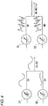
- Fig. 3A is a sectional view of the vicinity of the back plate 7 and the vibration electrode film 5 of the acoustic sensor 1 in the embodiment
- Fig. 3B is an equivalent circuit diagram obtained in that configuration.
- a change in capacitance between the vibration electrode film 5 and the fixed electrode film 8 of the back plate 7 is detected as an electrical signal
- a change in capacitance between the vibration electrode film 5 and the substrate 3 is also detected as an electrical signal. Both detected signals are added to each other to obtain a signal, which is taken as an output signal of the capacitive transducer. That is, in the embodiment, as illustrated in Fig.
- the vibration electrode film 5 and the fixed electrode film 8 of the back plate 7 are made to constitute a first capacitor C1
- the vibration electrode film 5 and the substrate 3 are made to constitute a second capacitor C2. Then, signals based on changes in capacitance of the first capacitor C1 and the second capacitor C2 are added to each other.
- the signal based on the change in capacitance of the first capacitor C1 (hereinafter also referred to as the signal from the first capacitor C1) and the signal based on the change in capacitance of the second capacitor C2 (hereinafter also referred to as the signal from the second capacitor C2) have reversed polarities.
- a noise of the signal from the first capacitor C1 and a noise of the signal from the second capacitor C2 also have reversed polarities.
- a ratio of levels of the signal from the first capacitor C1 and the signal from the second capacitor C2 is basically different from a ratio of noise levels concerning those signals. This is because, a generation process for the above noise is not necessarily the same as a generation process for the signal from the first capacitor C1 and the signal from the second capacitor C2.
- the level of the noise concerning the signal from the first capacitor C1 is matched with the level of the noise concerning the signal from the second capacitor C2. Accordingly, as illustrated in Fig. 4A , even after addition of a signal S1 from the first capacitor C1 and a signal S2 from the second capacitor C2, a signal S1 + S2 is left (S1 > S1 + S2, since S1 and S2 have reversed polarities). Meanwhile, as illustrated in Fig. 4B , after addition of a noise N1 concerning the signal from the first capacitor C1 and a noise N2 concerning the signal from the second capacitor C2, the obtained noise is substantially zero. Hence the SN ratio of the signal obtained as the acoustic sensor system can be improved as much as possible.
- the sensitivity of the change in the signal from the first capacitor C1 or the second capacitor C2 due to transformation of the vibration electrode film 5 can be expressed as Expression (5) below: Sensitivity ⁇ c ⁇ s ⁇ V / g where c is a constant representing a hardness of the vibration electrode film 5, s is an area of the vibration electrode film 5 constituting each capacitor, V is an inter-electrode voltage, and g is an inter-electrode gap. It is considered that Expression (5) substantially holds also for the noise concerning the signal from the first capacitor C1 or the second capacitor C2.
- hardnesses c1 and c2, areas s1 and s2, inter-electrode voltages V1 and V2, and inter-electrode gaps g1 and g2 of the vibration electrode film 5, which forms the first capacitor C1 and the second capacitor C2 illustrated in Fig. 5B are decided appropriately in terms of design. This allows matching between the noise concerning the signal from the first capacitor C1 and the noise concerning the signal from the second capacitor C2. Therefore, adding the noise concerning the signal from the first capacitor C1 and the noise concerning the signal from the second capacitor C2 enables both noises to be canceled and a total noise to be minimized.
- the hardnesses c1 and c2 of the vibration electrode film 5, which forms the first capacitor C1 and the second capacitor C2 can be decided as mutually different values by changing regions to be used for the first capacitor C1 and the second capacitor C2 in the vibration electrode film 5, while the material of the vibration electrode film 5 is the same.
- the signal from the first capacitor C1 and the signal from the second capacitor C2 are added to each other by wiring among the vibrating membrane electrode pad 9 on the vibration electrode film 5, which is the common electrode for both capacitors, the fixed electrode pad 10 on the fixed electrode film 8 of the back plate 7, and an electrode pad 13 on the substrate 3, or wiring in the ASIC adjacent to the acoustic sensor 1, or by calculation.
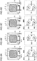
- Figs. 6A to 6D illustrate variations of wiring in that case.
- a structure made up of the vibration electrode film 5, the fixed electrode film 8 in the back plate 7, and the substrate 3 may be referred to as a MEMS with respect to the ASIC.
- VP means the vibration electrode film 5
- BP means the fixed electrode film 8 of the back plate 7, and
- Sub means the substrate 3.
- Fig 6A is an example where the vibrating membrane electrode pad 9 on the common vibration electrode film 5 in the MEMS is set to an output IN, and a voltage Volt1 is supplied from the ASIC to the fixed electrode pad 10 on the fixed electrode film 8, while a voltage Volt2 is supplied from the ASIC to the electrode pad 13 on the substrate 3.
- values of the voltages Volt1, Volt2 supplied from the ASIC can be adjusted as appropriate.
- the hardness c1 or c2 of the vibration electrode film 5, the area s1 or s2 of the vibration electrode film 5, and the inter-electrode gap g1 or g2 in the MEMS can be decided as appropriate.
- all the parameters represented in Expression (5) can be adjusted. It is thereby possible to more reliably improve the SN ratio as the acoustic sensor system with higher flexibility by matching the levels of the noises N1 and N2 concerning the signal S1 from the first capacitor C1 and the signal S2 from the second capacitor C2, while providing a certain difference between the levels of the respective signals.
- the parameters on the MEMS side the hardness c1 or c2 of the vibration electrode film 5, the area s1 or s2 of the vibration electrode film 5, and the inter-electrode gap g1 or g2 in the MEMS) can be adjusted.
- adjusting only the parameters on the MEMS side makes it possible to match the levels of the noises N1 and N2 concerning the signal S1 from the first capacitor C1 and the signal S2 from the second capacitor C2, while providing a certain difference between the levels of the respective signals, so as to improve the SN ratio as the acoustic sensor system.
- Fig 6C is an example where the voltage Volt is supplied to the vibrating membrane electrode pad 9 on the common vibration electrode film 5 in the MEMS, the fixed electrode pad 10 on the fixed electrode film 8 of the back plate 7 is set to a first output IN1, the electrode pad 13 on the substrate 3 is set to a second output IN2, and those INs are inputted into the ASIC.
- the hardness c1 or c2 of the vibration electrode film 5, the area s1 or s2 of the vibration electrode film 5, and the inter-electrode gap g1 or g2 in the MEMS are adjusted, high-level adjustment can be performed in the ASIC, such as application of appropriate gains and offsets to the first output IN1 and the second output IN2 in the ASIC. It is thereby possible to more reliably improve the SN ratio as the acoustic sensor system by matching the levels of the noises N1 and N2 concerning the signal S1 from the first capacitor C1 and the signal S2 from the second capacitor C2, while providing a certain difference between the levels of the respective signals.
- Fig 6D is an example where the common voltage Volt is supplied to the vibrating membrane electrode pad 9 on the common vibration electrode film 5, the output of the fixed electrode pad 10 on the fixed electrode film 8 of the back plate 7 and the output of the electrode pad 13 on the substrate 3 are connected, and then the output IN is inputted into the ASIC.
- the parameters on the MEMS side the hardness c1 or c2 of the vibration electrode film 5, the area s1 or s2 of the vibration electrode film 5, and the inter-electrode gap g1 or g2 in the MEMS are adjusted.
- adjusting only the parameters on the MEMS side makes it possible to match the levels of the noises N1 and N2 concerning the signal S1 from the first capacitor C1 and the signal S2 from the second capacitor C2, while providing a certain difference between the levels of the respective signals, so as to improve the SN ratio as the acoustic sensor system.
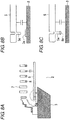
- the second capacitor C2 are formed of the vibration electrode film 5 and the substrate 3 in the embodiment, in this case, the whole or the surface of the substrate 3 may be made conductive as illustrated in Fig. 7A . This enables the substrate 3 to be used as it is as the fixed electrode, without providing an additional film formation process. Meanwhile, as illustrated in Fig. 7B , a conductive fixed electrode may be separately provided on the surface of the substrate 3 on the vibration electrode film 5 side. This facilitates adjustment of the area of the fixed electrode of the second capacitor C2, thus enabling adjustment of the level and the noise level of the signal from the second capacitor C2 in a simpler or more accurate manner.
- a stopper 5a for preventing sticking with the substrate 3 may be formed on the vibration electrode film 5.
- an insulation 3a made of an insulator may be formed on the substrate 3 as illustrated in Fig. 8B
- an insulation 5b made of an insulator may be provided at the tip of the stopper 5a on the vibration electrode film 5 as illustrated in Fig. 8C . It is thereby possible to prevent occurrence of an electrical short circuit when the vibration electrode film 5 and the substrate 3 come into contact with each other at the stopper 5a.
- Fig. 9A is a sectional view of the vicinity of the back plate 7 and the vibration electrode film 5 of the acoustic sensor 1 in the embodiment
- Fig. 9B is an equivalent circuit diagram obtained in that configuration.
- the fixed electrode film 8 of the back plate 7 is divided into a first fixed electrode film 8a and a second fixed electrode film 8b.
- the vibration electrode film 5 and the first fixed electrode film 8a constitute the first capacitor C1.
- the vibration electrode film 5 and the second fixed electrode film 8b constitute the second capacitor C2. That is, in the embodiment, both the first capacitor C1 and the second capacitor C2 are made up of the vibration electrode film 5 and the fixed electrode film 8 of the back plate 7.
- the signal from the first capacitor C1 and the signal from the second capacitor C2 have the same polarity, and the noise of the signal from the first capacitor C1 and the noise of the signal from the second capacitor C2 also have the same polarity. Accordingly, canceling the noises concerning the signals from the first capacitor C1 and the second capacitor C2 requires subtraction of the signal from the first capacitor C1 and the signal from the second capacitor C2, rather than addition of those signals.
- the output IN1 of the first capacitor C1 and the output IN2 of the second capacitor C2 are each inputted into the ASIC. Then, after IN2 is reversed in the ASIC, both outputs are added to each other. It is thereby possible to more reliably improve the SN ratio as the acoustic sensor system by matching the levels of the noises concerning the signal from the first capacitor C1 and the signal from the second capacitor C2 and canceling the noise of the signal from the first capacitor C1 and the noise of the signal from the second capacitor C2, while providing a certain difference between the levels of the respective signals.
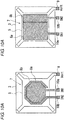
- Figs. 10A and 10B illustrate examples of a dividing method in the case of dividing the fixed electrode of the back plate 7 into the first fixed electrode film 8a and the second fixed electrode film 8b.
- the second fixed electrode film 8b may be disposed so as to enclose the first fixed electrode film 8a as illustrated in Fig. 10A , or the first fixed electrode film 8a and the second fixed electrode film 8b may be disposed side by side as illustrated in Fig. 10B .
Landscapes
- Physics & Mathematics (AREA)
- Engineering & Computer Science (AREA)
- Acoustics & Sound (AREA)
- Signal Processing (AREA)
- Electrostatic, Electromagnetic, Magneto- Strictive, And Variable-Resistance Transducers (AREA)
- Pressure Sensors (AREA)
- Circuit For Audible Band Transducer (AREA)
- Micromachines (AREA)
Applications Claiming Priority (1)
| Application Number | Priority Date | Filing Date | Title |
|---|---|---|---|
| JP2016238141A JP7143056B2 (ja) | 2016-12-08 | 2016-12-08 | 静電容量型トランスデューサシステム、静電容量型トランスデューサ及び、音響センサ |
Publications (3)
| Publication Number | Publication Date |
|---|---|
| EP3334183A2 true EP3334183A2 (fr) | 2018-06-13 |
| EP3334183A3 EP3334183A3 (fr) | 2018-06-27 |
| EP3334183B1 EP3334183B1 (fr) | 2023-04-19 |
Family
ID=60119923
Family Applications (1)
| Application Number | Title | Priority Date | Filing Date |
|---|---|---|---|
| EP17196739.1A Active EP3334183B1 (fr) | 2016-12-08 | 2017-10-17 | Système transducteur capacitif, transducteur capacitif et capteur acoustique |
Country Status (4)
| Country | Link |
|---|---|
| US (1) | US10412501B2 (fr) |
| EP (1) | EP3334183B1 (fr) |
| JP (1) | JP7143056B2 (fr) |
| CN (1) | CN108174333B (fr) |
Families Citing this family (5)
| Publication number | Priority date | Publication date | Assignee | Title |
|---|---|---|---|---|
| CN111277936B (zh) * | 2019-12-30 | 2021-08-10 | 瑞声声学科技(深圳)有限公司 | 一种mems麦克风 |
| EP4191318B1 (fr) * | 2020-07-31 | 2025-03-12 | FUJIFILM Corporation | Dispositif de balayage optique, son procédé de commande et système de dessin d'image |
| JP2023142356A (ja) * | 2022-03-25 | 2023-10-05 | Mmiセミコンダクター株式会社 | Memsマイクロフォン |
| CN115002631A (zh) * | 2022-04-20 | 2022-09-02 | 苏州敏芯微电子技术股份有限公司 | 麦克风组件及电子设备 |
| CN121013661A (zh) * | 2023-04-24 | 2025-11-25 | 菲利普莫里斯生产公司 | 用于气溶胶生成装置的改进的青少年访问预防 |
Citations (3)
| Publication number | Priority date | Publication date | Assignee | Title |
|---|---|---|---|---|
| US6714654B2 (en) | 2002-02-06 | 2004-03-30 | George Jay Lichtblau | Hearing aid operative to cancel sounds propagating through the hearing aid case |
| US20080144874A1 (en) | 2006-12-19 | 2008-06-19 | Fortemedia, Inc. | Microphone array with electromagnetic interference shielding means |
| JP2011250170A (ja) | 2010-05-27 | 2011-12-08 | Omron Corp | 音響センサ、音響トランスデューサ、該音響トランスデューサを利用したマイクロフォン、および音響トランスデューサの製造方法 |
Family Cites Families (19)
| Publication number | Priority date | Publication date | Assignee | Title |
|---|---|---|---|---|
| US6813954B2 (en) * | 2001-05-25 | 2004-11-09 | Panametrics, Inc. | High sensitivity pressure sensor with long term stability |
| WO2007024909A1 (fr) | 2005-08-23 | 2007-03-01 | Analog Devices, Inc. | Systeme multi-microphones |
| JP4770605B2 (ja) * | 2006-06-26 | 2011-09-14 | ヤマハ株式会社 | 平衡出力マイクロホンおよび平衡出力マイクロホンの製造方法 |
| US7888754B2 (en) * | 2007-12-28 | 2011-02-15 | Yamaha Corporation | MEMS transducer |
| WO2009105793A1 (fr) * | 2008-02-26 | 2009-09-03 | Akg Acoustics Gmbh | Ensemble transducteur |
| JP5769964B2 (ja) * | 2008-07-11 | 2015-08-26 | ローム株式会社 | Memsデバイス |
| JP2010098518A (ja) * | 2008-10-16 | 2010-04-30 | Rohm Co Ltd | Memsセンサの製造方法およびmemsセンサ |
| JPWO2010073598A1 (ja) * | 2008-12-24 | 2012-06-07 | パナソニック株式会社 | 平衡信号出力型センサー |
| JP2011193342A (ja) * | 2010-03-16 | 2011-09-29 | Panasonic Corp | Memsデバイス |
| US20130044899A1 (en) * | 2011-08-15 | 2013-02-21 | Harman International Industries, Inc. | Dual Backplate Microphone |
| JP6237978B2 (ja) | 2013-03-13 | 2017-11-29 | オムロン株式会社 | 静電容量型センサ、音響センサ及びマイクロフォン |
| US10589987B2 (en) * | 2013-11-06 | 2020-03-17 | Infineon Technologies Ag | System and method for a MEMS transducer |
| JP6264969B2 (ja) * | 2014-03-14 | 2018-01-24 | オムロン株式会社 | 音響トランスデューサ |
| US20150296307A1 (en) * | 2014-04-10 | 2015-10-15 | Knowles Electronics, Llc. | Dual diaphragm and dual back plate acoustic apparatus |
| US10165342B2 (en) | 2014-05-12 | 2018-12-25 | Tdk Corporation | Microphone assembly and method of manufacturing a microphone assembly |
| US9491531B2 (en) * | 2014-08-11 | 2016-11-08 | 3R Semiconductor Technology Inc. | Microphone device for reducing noise coupling effect |
| US10375482B2 (en) | 2015-03-12 | 2019-08-06 | Omron Corporation | Capacitance type transducer and acoustic sensor |
| CN205584497U (zh) * | 2016-05-09 | 2016-09-14 | 上海微联传感科技有限公司 | 硅麦克风 |
| US9936304B2 (en) * | 2016-08-23 | 2018-04-03 | Infineon Technologies Ag | Digital silicon microphone with configurable sensitivity, frequency response and noise transfer function |
-
2016
- 2016-12-08 JP JP2016238141A patent/JP7143056B2/ja active Active
-
2017
- 2017-10-17 EP EP17196739.1A patent/EP3334183B1/fr active Active
- 2017-10-18 CN CN201710970853.1A patent/CN108174333B/zh active Active
- 2017-11-09 US US15/808,736 patent/US10412501B2/en active Active
Patent Citations (3)
| Publication number | Priority date | Publication date | Assignee | Title |
|---|---|---|---|---|
| US6714654B2 (en) | 2002-02-06 | 2004-03-30 | George Jay Lichtblau | Hearing aid operative to cancel sounds propagating through the hearing aid case |
| US20080144874A1 (en) | 2006-12-19 | 2008-06-19 | Fortemedia, Inc. | Microphone array with electromagnetic interference shielding means |
| JP2011250170A (ja) | 2010-05-27 | 2011-12-08 | Omron Corp | 音響センサ、音響トランスデューサ、該音響トランスデューサを利用したマイクロフォン、および音響トランスデューサの製造方法 |
Also Published As
| Publication number | Publication date |
|---|---|
| JP2018098526A (ja) | 2018-06-21 |
| EP3334183B1 (fr) | 2023-04-19 |
| CN108174333B (zh) | 2020-07-07 |
| US10412501B2 (en) | 2019-09-10 |
| EP3334183A3 (fr) | 2018-06-27 |
| CN108174333A (zh) | 2018-06-15 |
| US20180167741A1 (en) | 2018-06-14 |
| JP7143056B2 (ja) | 2022-09-28 |
Similar Documents
| Publication | Publication Date | Title |
|---|---|---|
| EP3334183B1 (fr) | Système transducteur capacitif, transducteur capacitif et capteur acoustique | |
| US7245734B2 (en) | Directional microphone | |
| US10477322B2 (en) | MEMS device and process | |
| US10626007B2 (en) | Microelectromechanical transducer | |
| KR101318332B1 (ko) | 음파센서 및 마이크로폰 | |
| EP2320678B1 (fr) | Dispositif de microphone avec accéléromètre pour compensation de vibrations | |
| JP4552883B2 (ja) | 振動検出方法 | |
| EP2974365B1 (fr) | Microphone différentiel ayant polarisation à double polarité | |
| JP5325630B2 (ja) | マイクロホン装置並びにその調整装置及び調整方法 | |
| EP3457098A1 (fr) | Dispositif d'analyse de spectre de vibrations/sonore et procédés d'acquisition et d'analyse d'informations de fréquence | |
| GB2515836A (en) | MEMS device and process | |
| TWI457270B (zh) | 微機電系統裝置及製程 | |
| JPWO2018207578A1 (ja) | 圧電マイクロフォンチップおよび圧電マイクロフォン | |
| US20180002161A1 (en) | Mems device and process | |
| US20250178883A1 (en) | Vibration sensor | |
| CN109848022A (zh) | 超声波器件以及超声波测量装置 | |
| JP6908324B2 (ja) | 圧電素子 | |
| US10730747B2 (en) | MEMS devices and processes | |
| JPWO2018061805A1 (ja) | 圧電式マイクロフォン | |
| JP6867789B2 (ja) | Memsマイクロフォン | |
| JP2008259062A (ja) | 静電型トランスデューサ | |
| US20190075401A1 (en) | Mems devices and processes | |
| JP4672539B2 (ja) | コンデンサマイクロホン装置 | |
| JP7125004B2 (ja) | Mems素子 | |
| JP2025155881A (ja) | 音響変換装置 |
Legal Events
| Date | Code | Title | Description |
|---|---|---|---|
| PUAI | Public reference made under article 153(3) epc to a published international application that has entered the european phase |
Free format text: ORIGINAL CODE: 0009012 |
|
| STAA | Information on the status of an ep patent application or granted ep patent |
Free format text: STATUS: THE APPLICATION HAS BEEN PUBLISHED |
|
| PUAL | Search report despatched |
Free format text: ORIGINAL CODE: 0009013 |
|
| AK | Designated contracting states |
Kind code of ref document: A2 Designated state(s): AL AT BE BG CH CY CZ DE DK EE ES FI FR GB GR HR HU IE IS IT LI LT LU LV MC MK MT NL NO PL PT RO RS SE SI SK SM TR |
|
| AX | Request for extension of the european patent |
Extension state: BA ME |
|
| AK | Designated contracting states |
Kind code of ref document: A3 Designated state(s): AL AT BE BG CH CY CZ DE DK EE ES FI FR GB GR HR HU IE IS IT LI LT LU LV MC MK MT NL NO PL PT RO RS SE SI SK SM TR |
|
| AX | Request for extension of the european patent |
Extension state: BA ME |
|
| RIC1 | Information provided on ipc code assigned before grant |
Ipc: H04R 19/04 20060101ALI20180523BHEP Ipc: H04R 19/00 20060101AFI20180523BHEP |
|
| STAA | Information on the status of an ep patent application or granted ep patent |
Free format text: STATUS: REQUEST FOR EXAMINATION WAS MADE |
|
| 17P | Request for examination filed |
Effective date: 20180831 |
|
| RBV | Designated contracting states (corrected) |
Designated state(s): AL AT BE BG CH CY CZ DE DK EE ES FI FR GB GR HR HU IE IS IT LI LT LU LV MC MK MT NL NO PL PT RO RS SE SI SK SM TR |
|
| STAA | Information on the status of an ep patent application or granted ep patent |
Free format text: STATUS: EXAMINATION IS IN PROGRESS |
|
| 17Q | First examination report despatched |
Effective date: 20200612 |
|
| RAP1 | Party data changed (applicant data changed or rights of an application transferred) |
Owner name: MMI SEMICONDUCTOR CO., LTD. |
|
| GRAP | Despatch of communication of intention to grant a patent |
Free format text: ORIGINAL CODE: EPIDOSNIGR1 |
|
| STAA | Information on the status of an ep patent application or granted ep patent |
Free format text: STATUS: GRANT OF PATENT IS INTENDED |
|
| INTG | Intention to grant announced |
Effective date: 20221110 |
|
| GRAS | Grant fee paid |
Free format text: ORIGINAL CODE: EPIDOSNIGR3 |
|
| GRAA | (expected) grant |
Free format text: ORIGINAL CODE: 0009210 |
|
| STAA | Information on the status of an ep patent application or granted ep patent |
Free format text: STATUS: THE PATENT HAS BEEN GRANTED |
|
| AK | Designated contracting states |
Kind code of ref document: B1 Designated state(s): AL AT BE BG CH CY CZ DE DK EE ES FI FR GB GR HR HU IE IS IT LI LT LU LV MC MK MT NL NO PL PT RO RS SE SI SK SM TR |
|
| REG | Reference to a national code |
Ref country code: GB Ref legal event code: FG4D |
|
| REG | Reference to a national code |
Ref country code: DE Ref legal event code: R096 Ref document number: 602017067793 Country of ref document: DE |
|
| REG | Reference to a national code |
Ref country code: CH Ref legal event code: EP |
|
| REG | Reference to a national code |
Ref country code: IE Ref legal event code: FG4D |
|
| REG | Reference to a national code |
Ref country code: AT Ref legal event code: REF Ref document number: 1562088 Country of ref document: AT Kind code of ref document: T Effective date: 20230515 |
|
| REG | Reference to a national code |
Ref country code: LT Ref legal event code: MG9D |
|
| REG | Reference to a national code |
Ref country code: NL Ref legal event code: MP Effective date: 20230419 |
|
| REG | Reference to a national code |
Ref country code: AT Ref legal event code: MK05 Ref document number: 1562088 Country of ref document: AT Kind code of ref document: T Effective date: 20230419 |
|
| PG25 | Lapsed in a contracting state [announced via postgrant information from national office to epo] |
Ref country code: NL Free format text: LAPSE BECAUSE OF FAILURE TO SUBMIT A TRANSLATION OF THE DESCRIPTION OR TO PAY THE FEE WITHIN THE PRESCRIBED TIME-LIMIT Effective date: 20230419 |
|
| PG25 | Lapsed in a contracting state [announced via postgrant information from national office to epo] |
Ref country code: SE Free format text: LAPSE BECAUSE OF FAILURE TO SUBMIT A TRANSLATION OF THE DESCRIPTION OR TO PAY THE FEE WITHIN THE PRESCRIBED TIME-LIMIT Effective date: 20230419 Ref country code: PT Free format text: LAPSE BECAUSE OF FAILURE TO SUBMIT A TRANSLATION OF THE DESCRIPTION OR TO PAY THE FEE WITHIN THE PRESCRIBED TIME-LIMIT Effective date: 20230821 Ref country code: NO Free format text: LAPSE BECAUSE OF FAILURE TO SUBMIT A TRANSLATION OF THE DESCRIPTION OR TO PAY THE FEE WITHIN THE PRESCRIBED TIME-LIMIT Effective date: 20230719 Ref country code: ES Free format text: LAPSE BECAUSE OF FAILURE TO SUBMIT A TRANSLATION OF THE DESCRIPTION OR TO PAY THE FEE WITHIN THE PRESCRIBED TIME-LIMIT Effective date: 20230419 Ref country code: AT Free format text: LAPSE BECAUSE OF FAILURE TO SUBMIT A TRANSLATION OF THE DESCRIPTION OR TO PAY THE FEE WITHIN THE PRESCRIBED TIME-LIMIT Effective date: 20230419 |
|
| PG25 | Lapsed in a contracting state [announced via postgrant information from national office to epo] |
Ref country code: RS Free format text: LAPSE BECAUSE OF FAILURE TO SUBMIT A TRANSLATION OF THE DESCRIPTION OR TO PAY THE FEE WITHIN THE PRESCRIBED TIME-LIMIT Effective date: 20230419 Ref country code: PL Free format text: LAPSE BECAUSE OF FAILURE TO SUBMIT A TRANSLATION OF THE DESCRIPTION OR TO PAY THE FEE WITHIN THE PRESCRIBED TIME-LIMIT Effective date: 20230419 Ref country code: LV Free format text: LAPSE BECAUSE OF FAILURE TO SUBMIT A TRANSLATION OF THE DESCRIPTION OR TO PAY THE FEE WITHIN THE PRESCRIBED TIME-LIMIT Effective date: 20230419 Ref country code: LT Free format text: LAPSE BECAUSE OF FAILURE TO SUBMIT A TRANSLATION OF THE DESCRIPTION OR TO PAY THE FEE WITHIN THE PRESCRIBED TIME-LIMIT Effective date: 20230419 Ref country code: IS Free format text: LAPSE BECAUSE OF FAILURE TO SUBMIT A TRANSLATION OF THE DESCRIPTION OR TO PAY THE FEE WITHIN THE PRESCRIBED TIME-LIMIT Effective date: 20230819 Ref country code: HR Free format text: LAPSE BECAUSE OF FAILURE TO SUBMIT A TRANSLATION OF THE DESCRIPTION OR TO PAY THE FEE WITHIN THE PRESCRIBED TIME-LIMIT Effective date: 20230419 Ref country code: GR Free format text: LAPSE BECAUSE OF FAILURE TO SUBMIT A TRANSLATION OF THE DESCRIPTION OR TO PAY THE FEE WITHIN THE PRESCRIBED TIME-LIMIT Effective date: 20230720 Ref country code: AL Free format text: LAPSE BECAUSE OF FAILURE TO SUBMIT A TRANSLATION OF THE DESCRIPTION OR TO PAY THE FEE WITHIN THE PRESCRIBED TIME-LIMIT Effective date: 20230419 |
|
| PG25 | Lapsed in a contracting state [announced via postgrant information from national office to epo] |
Ref country code: FI Free format text: LAPSE BECAUSE OF FAILURE TO SUBMIT A TRANSLATION OF THE DESCRIPTION OR TO PAY THE FEE WITHIN THE PRESCRIBED TIME-LIMIT Effective date: 20230419 |
|
| PG25 | Lapsed in a contracting state [announced via postgrant information from national office to epo] |
Ref country code: SK Free format text: LAPSE BECAUSE OF FAILURE TO SUBMIT A TRANSLATION OF THE DESCRIPTION OR TO PAY THE FEE WITHIN THE PRESCRIBED TIME-LIMIT Effective date: 20230419 |
|
| REG | Reference to a national code |
Ref country code: DE Ref legal event code: R097 Ref document number: 602017067793 Country of ref document: DE |
|
| PG25 | Lapsed in a contracting state [announced via postgrant information from national office to epo] |
Ref country code: SM Free format text: LAPSE BECAUSE OF FAILURE TO SUBMIT A TRANSLATION OF THE DESCRIPTION OR TO PAY THE FEE WITHIN THE PRESCRIBED TIME-LIMIT Effective date: 20230419 Ref country code: SK Free format text: LAPSE BECAUSE OF FAILURE TO SUBMIT A TRANSLATION OF THE DESCRIPTION OR TO PAY THE FEE WITHIN THE PRESCRIBED TIME-LIMIT Effective date: 20230419 Ref country code: RO Free format text: LAPSE BECAUSE OF FAILURE TO SUBMIT A TRANSLATION OF THE DESCRIPTION OR TO PAY THE FEE WITHIN THE PRESCRIBED TIME-LIMIT Effective date: 20230419 Ref country code: EE Free format text: LAPSE BECAUSE OF FAILURE TO SUBMIT A TRANSLATION OF THE DESCRIPTION OR TO PAY THE FEE WITHIN THE PRESCRIBED TIME-LIMIT Effective date: 20230419 Ref country code: DK Free format text: LAPSE BECAUSE OF FAILURE TO SUBMIT A TRANSLATION OF THE DESCRIPTION OR TO PAY THE FEE WITHIN THE PRESCRIBED TIME-LIMIT Effective date: 20230419 Ref country code: CZ Free format text: LAPSE BECAUSE OF FAILURE TO SUBMIT A TRANSLATION OF THE DESCRIPTION OR TO PAY THE FEE WITHIN THE PRESCRIBED TIME-LIMIT Effective date: 20230419 |
|
| PLBE | No opposition filed within time limit |
Free format text: ORIGINAL CODE: 0009261 |
|
| STAA | Information on the status of an ep patent application or granted ep patent |
Free format text: STATUS: NO OPPOSITION FILED WITHIN TIME LIMIT |
|
| 26N | No opposition filed |
Effective date: 20240122 |
|
| PG25 | Lapsed in a contracting state [announced via postgrant information from national office to epo] |
Ref country code: SI Free format text: LAPSE BECAUSE OF FAILURE TO SUBMIT A TRANSLATION OF THE DESCRIPTION OR TO PAY THE FEE WITHIN THE PRESCRIBED TIME-LIMIT Effective date: 20230419 |
|
| PG25 | Lapsed in a contracting state [announced via postgrant information from national office to epo] |
Ref country code: SI Free format text: LAPSE BECAUSE OF FAILURE TO SUBMIT A TRANSLATION OF THE DESCRIPTION OR TO PAY THE FEE WITHIN THE PRESCRIBED TIME-LIMIT Effective date: 20230419 Ref country code: IT Free format text: LAPSE BECAUSE OF FAILURE TO SUBMIT A TRANSLATION OF THE DESCRIPTION OR TO PAY THE FEE WITHIN THE PRESCRIBED TIME-LIMIT Effective date: 20230419 Ref country code: MC Free format text: LAPSE BECAUSE OF FAILURE TO SUBMIT A TRANSLATION OF THE DESCRIPTION OR TO PAY THE FEE WITHIN THE PRESCRIBED TIME-LIMIT Effective date: 20230419 |
|
| REG | Reference to a national code |
Ref country code: CH Ref legal event code: PL |
|
| REG | Reference to a national code |
Ref country code: BE Ref legal event code: MM Effective date: 20231031 |
|
| PG25 | Lapsed in a contracting state [announced via postgrant information from national office to epo] |
Ref country code: LU Free format text: LAPSE BECAUSE OF NON-PAYMENT OF DUE FEES Effective date: 20231017 |
|
| GBPC | Gb: european patent ceased through non-payment of renewal fee |
Effective date: 20231017 |
|
| PG25 | Lapsed in a contracting state [announced via postgrant information from national office to epo] |
Ref country code: LU Free format text: LAPSE BECAUSE OF NON-PAYMENT OF DUE FEES Effective date: 20231017 |
|
| PG25 | Lapsed in a contracting state [announced via postgrant information from national office to epo] |
Ref country code: GB Free format text: LAPSE BECAUSE OF NON-PAYMENT OF DUE FEES Effective date: 20231017 |
|
| PG25 | Lapsed in a contracting state [announced via postgrant information from national office to epo] |
Ref country code: CH Free format text: LAPSE BECAUSE OF NON-PAYMENT OF DUE FEES Effective date: 20231031 |
|
| PG25 | Lapsed in a contracting state [announced via postgrant information from national office to epo] |
Ref country code: GB Free format text: LAPSE BECAUSE OF NON-PAYMENT OF DUE FEES Effective date: 20231017 Ref country code: FR Free format text: LAPSE BECAUSE OF NON-PAYMENT OF DUE FEES Effective date: 20231031 Ref country code: CH Free format text: LAPSE BECAUSE OF NON-PAYMENT OF DUE FEES Effective date: 20231031 |
|
| PG25 | Lapsed in a contracting state [announced via postgrant information from national office to epo] |
Ref country code: BE Free format text: LAPSE BECAUSE OF NON-PAYMENT OF DUE FEES Effective date: 20231031 |
|
| PG25 | Lapsed in a contracting state [announced via postgrant information from national office to epo] |
Ref country code: IE Free format text: LAPSE BECAUSE OF NON-PAYMENT OF DUE FEES Effective date: 20231017 |
|
| PG25 | Lapsed in a contracting state [announced via postgrant information from national office to epo] |
Ref country code: IE Free format text: LAPSE BECAUSE OF NON-PAYMENT OF DUE FEES Effective date: 20231017 |
|
| PG25 | Lapsed in a contracting state [announced via postgrant information from national office to epo] |
Ref country code: BG Free format text: LAPSE BECAUSE OF FAILURE TO SUBMIT A TRANSLATION OF THE DESCRIPTION OR TO PAY THE FEE WITHIN THE PRESCRIBED TIME-LIMIT Effective date: 20230419 |
|
| PG25 | Lapsed in a contracting state [announced via postgrant information from national office to epo] |
Ref country code: BG Free format text: LAPSE BECAUSE OF FAILURE TO SUBMIT A TRANSLATION OF THE DESCRIPTION OR TO PAY THE FEE WITHIN THE PRESCRIBED TIME-LIMIT Effective date: 20230419 |
|
| PGFP | Annual fee paid to national office [announced via postgrant information from national office to epo] |
Ref country code: DE Payment date: 20241021 Year of fee payment: 8 |
|
| PG25 | Lapsed in a contracting state [announced via postgrant information from national office to epo] |
Ref country code: CY Free format text: LAPSE BECAUSE OF FAILURE TO SUBMIT A TRANSLATION OF THE DESCRIPTION OR TO PAY THE FEE WITHIN THE PRESCRIBED TIME-LIMIT; INVALID AB INITIO Effective date: 20171017 |
|
| PG25 | Lapsed in a contracting state [announced via postgrant information from national office to epo] |
Ref country code: HU Free format text: LAPSE BECAUSE OF FAILURE TO SUBMIT A TRANSLATION OF THE DESCRIPTION OR TO PAY THE FEE WITHIN THE PRESCRIBED TIME-LIMIT; INVALID AB INITIO Effective date: 20171017 |
|
| PG25 | Lapsed in a contracting state [announced via postgrant information from national office to epo] |
Ref country code: TR Free format text: LAPSE BECAUSE OF FAILURE TO SUBMIT A TRANSLATION OF THE DESCRIPTION OR TO PAY THE FEE WITHIN THE PRESCRIBED TIME-LIMIT Effective date: 20230419 |