EP3334255B1 - Beleuchtungswerkzeug für fahrzeug und lichtquellenbeleuchtungsschaltung - Google Patents
Beleuchtungswerkzeug für fahrzeug und lichtquellenbeleuchtungsschaltung Download PDFInfo
- Publication number
- EP3334255B1 EP3334255B1 EP16832912.6A EP16832912A EP3334255B1 EP 3334255 B1 EP3334255 B1 EP 3334255B1 EP 16832912 A EP16832912 A EP 16832912A EP 3334255 B1 EP3334255 B1 EP 3334255B1
- Authority
- EP
- European Patent Office
- Prior art keywords
- signal
- voltage
- structured
- circuit
- frequency
- Prior art date
- Legal status (The legal status is an assumption and is not a legal conclusion. Google has not performed a legal analysis and makes no representation as to the accuracy of the status listed.)
- Not-in-force
Links
Images












Classifications
-
- H—ELECTRICITY
- H05—ELECTRIC TECHNIQUES NOT OTHERWISE PROVIDED FOR
- H05B—ELECTRIC HEATING; ELECTRIC LIGHT SOURCES NOT OTHERWISE PROVIDED FOR; CIRCUIT ARRANGEMENTS FOR ELECTRIC LIGHT SOURCES, IN GENERAL
- H05B45/00—Circuit arrangements for operating light-emitting diodes [LED]
- H05B45/40—Details of LED load circuits
- H05B45/44—Details of LED load circuits with an active control inside an LED matrix
- H05B45/48—Details of LED load circuits with an active control inside an LED matrix having LEDs organised in strings and incorporating parallel shunting devices
-
- B—PERFORMING OPERATIONS; TRANSPORTING
- B60—VEHICLES IN GENERAL
- B60Q—ARRANGEMENT OF SIGNALLING OR LIGHTING DEVICES, THE MOUNTING OR SUPPORTING THEREOF OR CIRCUITS THEREFOR, FOR VEHICLES IN GENERAL
- B60Q1/00—Arrangement of optical signalling or lighting devices, the mounting or supporting thereof or circuits therefor
- B60Q1/02—Arrangement of optical signalling or lighting devices, the mounting or supporting thereof or circuits therefor the devices being primarily intended to illuminate the way ahead or to illuminate other areas of way or environments
- B60Q1/04—Arrangement of optical signalling or lighting devices, the mounting or supporting thereof or circuits therefor the devices being primarily intended to illuminate the way ahead or to illuminate other areas of way or environments the devices being headlights
-
- B—PERFORMING OPERATIONS; TRANSPORTING
- B60—VEHICLES IN GENERAL
- B60Q—ARRANGEMENT OF SIGNALLING OR LIGHTING DEVICES, THE MOUNTING OR SUPPORTING THEREOF OR CIRCUITS THEREFOR, FOR VEHICLES IN GENERAL
- B60Q1/00—Arrangement of optical signalling or lighting devices, the mounting or supporting thereof or circuits therefor
- B60Q1/02—Arrangement of optical signalling or lighting devices, the mounting or supporting thereof or circuits therefor the devices being primarily intended to illuminate the way ahead or to illuminate other areas of way or environments
- B60Q1/04—Arrangement of optical signalling or lighting devices, the mounting or supporting thereof or circuits therefor the devices being primarily intended to illuminate the way ahead or to illuminate other areas of way or environments the devices being headlights
- B60Q1/14—Arrangement of optical signalling or lighting devices, the mounting or supporting thereof or circuits therefor the devices being primarily intended to illuminate the way ahead or to illuminate other areas of way or environments the devices being headlights having dimming means
- B60Q1/1407—General lighting circuits comprising dimming circuits
-
- H—ELECTRICITY
- H02—GENERATION; CONVERSION OR DISTRIBUTION OF ELECTRIC POWER
- H02M—APPARATUS FOR CONVERSION BETWEEN AC AND AC, BETWEEN AC AND DC, OR BETWEEN DC AND DC, AND FOR USE WITH MAINS OR SIMILAR POWER SUPPLY SYSTEMS; CONVERSION OF DC OR AC INPUT POWER INTO SURGE OUTPUT POWER; CONTROL OR REGULATION THEREOF
- H02M3/00—Conversion of DC power input into DC power output
- H02M3/02—Conversion of DC power input into DC power output without intermediate conversion into AC
- H02M3/04—Conversion of DC power input into DC power output without intermediate conversion into AC by static converters
- H02M3/10—Conversion of DC power input into DC power output without intermediate conversion into AC by static converters using discharge tubes with control electrode or semiconductor devices with control electrode
- H02M3/145—Conversion of DC power input into DC power output without intermediate conversion into AC by static converters using discharge tubes with control electrode or semiconductor devices with control electrode using devices of a triode or transistor type requiring continuous application of a control signal
- H02M3/155—Conversion of DC power input into DC power output without intermediate conversion into AC by static converters using discharge tubes with control electrode or semiconductor devices with control electrode using devices of a triode or transistor type requiring continuous application of a control signal using semiconductor devices only
-
- H—ELECTRICITY
- H05—ELECTRIC TECHNIQUES NOT OTHERWISE PROVIDED FOR
- H05B—ELECTRIC HEATING; ELECTRIC LIGHT SOURCES NOT OTHERWISE PROVIDED FOR; CIRCUIT ARRANGEMENTS FOR ELECTRIC LIGHT SOURCES, IN GENERAL
- H05B45/00—Circuit arrangements for operating light-emitting diodes [LED]
- H05B45/10—Controlling the intensity of the light
-
- H—ELECTRICITY
- H05—ELECTRIC TECHNIQUES NOT OTHERWISE PROVIDED FOR
- H05B—ELECTRIC HEATING; ELECTRIC LIGHT SOURCES NOT OTHERWISE PROVIDED FOR; CIRCUIT ARRANGEMENTS FOR ELECTRIC LIGHT SOURCES, IN GENERAL
- H05B45/00—Circuit arrangements for operating light-emitting diodes [LED]
- H05B45/30—Driver circuits
- H05B45/37—Converter circuits
- H05B45/3725—Switched mode power supply [SMPS]
-
- Y—GENERAL TAGGING OF NEW TECHNOLOGICAL DEVELOPMENTS; GENERAL TAGGING OF CROSS-SECTIONAL TECHNOLOGIES SPANNING OVER SEVERAL SECTIONS OF THE IPC; TECHNICAL SUBJECTS COVERED BY FORMER USPC CROSS-REFERENCE ART COLLECTIONS [XRACs] AND DIGESTS
- Y02—TECHNOLOGIES OR APPLICATIONS FOR MITIGATION OR ADAPTATION AGAINST CLIMATE CHANGE
- Y02B—CLIMATE CHANGE MITIGATION TECHNOLOGIES RELATED TO BUILDINGS, e.g. HOUSING, HOUSE APPLIANCES OR RELATED END-USER APPLICATIONS
- Y02B20/00—Energy efficient lighting technologies, e.g. halogen lamps or gas discharge lamps
- Y02B20/30—Semiconductor lamps, e.g. solid state lamps [SSL] light emitting diodes [LED] or organic LED [OLED]
Definitions
- the present invention relates to a lighting circuit for a semiconductor light source according to the preamble of claim 1.
- Typical vehicular lamps are capable of switching between a low-beam mode and a high-beam mode.
- the low-beam mode is used to illuminate a close range with a predetermined light intensity.
- light distribution is determined so as to prevent glare being imparted to an oncoming vehicle or a leading vehicle.
- the low-beam mode is mainly used when the vehicle is traveling in an urban area.
- the high-beam mode is used to illuminate a distant range over a wide area ahead of the vehicle with a relatively high light intensity.
- the high-beam mode is mainly used when the vehicle is traveling at high speed along a road where there are a small number of oncoming vehicles and leading vehicles.
- the high-beam mode provides the driver with high visibility, which is an advantage, as compared with the low-beam mode.
- this leads to a problem of imparting glare to a pedestrian or otherwise a driver of a leading vehicle ahead of the vehicle.
- the ADB (Adaptive Driving Beam) technique in which a high-beam distribution pattern is dynamically and adaptively controlled based on the state of the surroundings of a vehicle.
- the ADB technique the presence or absence of a leading vehicle, an oncoming vehicle, or a pedestrian ahead of the vehicle is detected, and illumination is reduced or otherwise turned off for a region that corresponds to such a vehicle or pedestrian thus detected, thereby reducing glare imparted to such a vehicle or pedestrian.
- a switching converter is used to turn on a light source of an vehicular lamp.
- ADB control operation there is a need to turn on and off the light source at high speed and to change the light amount at high speed.
- the present inventor has investigated an arrangement employing a hysteresis control method (which is also referred to as "Bang-Bang control” or “ripple control") that provides high responsivity.
- Fig. 1 is a block diagram showing a vehicular lamp employing a hysteresis control method investigated by the present inventors. It should be noted that this comparison technique thus investigated should not be recognized as a known technique.
- a vehicular lamp 1r includes a semiconductor light source 10 and a lighting circuit 20r.
- the semiconductor light source 10 includes a semiconductor device such as an LED (light-emitting diode), an LD (laser diode), or the like.
- the lighting circuit 20r includes a switching converter 30r, an output filter 31, and a converter controller 32r.
- the switching converter 30r receives a battery voltage V BAT (which will also be referred to as the "input voltage V IN ") from a battery 2 via a switch 4, and supplies a lamp current (driving current) I LAMP to the semiconductor light source 10.
- V BAT battery voltage
- V IN input voltage
- I LAMP lamp current (driving current) I LAMP to the semiconductor light source 10.
- the switching converter 30r is configured as a step-down converter (Buck converter) including an input capacitor C1, a switching transistor M1, a diode D1, and an inductor L1.
- the converter controller 32r detects a coil current I L of the switching converter 30r (i.e., output current of the step-down converter), and adjusts the duty ratio of the switching of the switching transistor M1 such that the output current I LAMP that corresponds to the coil current I L matches a target current I REF that corresponds to a target light amount of the semiconductor light source 10.
- the converter controller 32r is configured as a controller employing a hysteresis control method, including a current detection circuit 34, a hysteresis comparator 36, and a driver 38.
- a current sensing resistor (which will be referred to as the "sensing resistor” hereafter) R CS is arranged on a path of the coil current I L .
- a voltage drop occurs across the sensing resistor R CS in proportion to the coil current I L .
- the current detection circuit 34 generates a current detection signal V CS that represents the present coil current I L based on the voltage drop across the sensing resistor R CS
- the hysteresis comparator 36 compares the current detection signal V CS with a pair of threshold signals V THL and V THH determined according to a reference voltage V REF , and generates a control pulse S CNT that corresponds to a comparison result. Specifically, when the current detection signal V CS reaches an upper threshold signal V THH that corresponds to a peak value I PEAK of the coil current I L , the control pulse S CNT is switched to a first level. When the current detection signal V CS reaches a lower threshold signal V THL that corresponds to a bottom value I BOTTOM of the coil current I L , the control pulse S CNT is switched to a second level.
- the driver 38 drives the switching transistor M1 according to the control pulse S CNT .
- the coil current I L reciprocates between the peak value I PEAK and the bottom value I BOTTOM .
- a capacitor C2 and an inductor L2 form an output filter (current smoothing filter) 31, and smooth the coil current I L so as to generate the lamp current I LAMP .
- the lamp current I LAMP thus obtained is supplied to the semiconductor light source 10.
- European Patent Application No. 2852258 describes a semiconductor light source control device includes a driver circuit, which generates a drive current flowing through a plurality of LEDs connected in series and bypass switches, which are on-off controlled by a control signal. When the control signal indicates the off-state of the bypass switches, a voltage across the corresponding LEDs is clamped at an upper limit voltage by using the bypass switches.
- European Patent Application No. 2234255 describes a switching regulator, which supplies a controllable stable average current to a load, such as series-connected light emitting diodes.
- US Patent Application No. US2014/070728 describes a circuit for driving light emitting diodes includes a first semiconductor switch that is responsive to a driver signal and a freewheeling device coupled between a first supply terminal that provides a supply voltage and a second supply terminal that provides a reference potential.
- Japanese Patent Publication No. JP2014-216600 describes a LED lighting circuit with a primary circuit, a secondary circuit, and a transmission capacitor provided between the primary circuit and the secondary circuit, and a control part for suppressing variations in the on/off frequency of a switching element of a control device when either of or both of an input voltage and an output voltage are varied.
- JP2013-093214 describes a semiconductor light source lighting circuit having further excellent responsibility to load variation, which includes a transformer; a first switching element; a first diode and a second diode; an inductor and a control circuit that turns off the first switching element when the magnitude of an output current exceeds a first threshold value and turns on the first switching element when the value falls below a second threshold value.
- JP2009-009817 describes a fist light emitting module having first LEDs and a second light emitting module having second LEDs having a color temperature different from that of the first LEDs, and which are connected to a constant current power source in parallel.
- Such a converter employing the hysteresis control method has an advantage of high-speed responsivity.
- this arrangement has a disadvantage from the viewpoint of stability of the switching frequency and stability of the output as compared with a constant current control method employing an error amplifier.
- the present invention has been made in order to solve such a problem. Accordingly, it is an exemplary purpose of an embodiment of the present invention to provide a converter having at least one improved characteristic.
- An embodiment of the present invention relates to a lighting circuit.
- the lighting circuit comprises: a switching converter structured to supply electric power to a semiconductor light source; and a converter controller structured to control the switching converter.
- the converter controller comprises: a current detection circuit structured to generate a current detection signal that corresponds to a driving current supplied from the switching converter to the semiconductor light source; a hysteresis comparator structured to compare the current detection signal with an upper threshold signal and a lower threshold signal, and to generate a control pulse according to a comparison result; and a driver structured to drive a switching transistor of the switching converter according to the control pulse.
- the voltage difference between the upper threshold signal and the lower threshold signal is changed such that a frequency of the control pulse approaches a target value thereof.
- the switching frequency can be stabilized regardless of fluctuation of the input voltage or the output voltage, or otherwise variation in the inductance.
- the lighting circuit may further comprise: a frequency detection circuit structured to generate a frequency detection signal that indicates a frequency of the control pulse; and a threshold voltage adjustment circuit structured to change a voltage difference between the upper threshold signal and the lower threshold signal such that the frequency detection signal approaches a reference value.
- the threshold voltage adjustment circuit may comprise: an error signal generating circuit structured to generate a frequency error signal that corresponds to a difference between the frequency detection signal and the reference value; and a voltage source structured to generate an upper voltage and a lower voltage, and to change a voltage difference between the upper voltage and the lower voltage according to the frequency error signal.
- the hysteresis comparator may comprise: a selector structured to receive the upper voltage and the lower voltage, and to select one from among the upper voltage and the lower voltage according to the control pulse; and a first comparator structured to compare the current detection signal with a threshold voltage that corresponds to an output of the selector.
- the voltage source may comprise: a first terminal at which the upper voltage is developed; a second terminal at which the lower voltage is developed; a first resistor arranged between a fixed voltage line and the first terminal; a first transistor arranged between the first terminal and the second terminal; a second resistor arranged between the second terminal and a ground line; and an operational amplifier having an output coupled to a control terminal of the transistor, one input terminal coupled to receive the frequency error signal, and the other input terminal coupled to the second terminal.
- the error signal generating circuit may comprise a second comparator structured to generate a pulse signal that indicates a comparison result between the frequency detection signal and a reference value, and a low-pass filter structured to smooth the output signal of the second comparator.
- the error signal generating circuit may comprise an error amplifier.
- the frequency detection signal detection circuit may comprise a F/V conversion circuit.
- the frequency detection circuit may comprise a high-pass filter coupled to receive a control pulse or otherwise a gate pulse of the switching transistor, a first capacitor, a charger circuit structured to charge the first capacitor, and a second transistor structured to discharge the first capacitor according to the output signal of the high-pass filter.
- the frequency detection circuit may output a frequency detection signal that corresponds to the amplitude of a first periodic signal that occurs across the first capacitor.
- the frequency detection circuit may further comprise a peak hold circuit structured to receive the first periodic signal, and to output a frequency detection signal that indicates the peak value of the first periodic signal.
- the frequency detection circuit may further comprise an averaging circuit structured to receive the first periodic signal, and to output a frequency detection signal that indicates an average value of the first periodic signal.
- the lighting circuit may further comprise a modulator structured to generate a modulation signal having a lower frequency than a switching frequency of the switching transistor, and to modulate a difference between the upper threshold signal and the lower threshold signal according to the modulation signal.
- the lighting circuit may further comprise a modulator structured to superimpose, on a reference value, a modulation signal having a lower frequency than a switching frequency of the switching transistor.
- the modulator may comprise an oscillator structured to generate a modulation signal having any one from among a triangle wave, a sawtooth wave, a ramp wave, a sine wave, and a trapezoidal wave.
- the converter controller may be structured to receive a pulse dimming signal that has been pulse modulated according to a target light amount for the semiconductor light source, and to alternately repeat an operating period in which the switching transistor is switched on and off and a suspension period in which the switching is suspended. Also, during the suspension period, the threshold voltage adjustment circuit may hold the frequency detection signal at a level that has been set in the immediately previous operating period.
- this arrangement provides improved frequency stability in the pulse dimming operation.
- the error signal generating circuit may comprise: a second comparator structured to generate a pulse signal that indicates a comparison result between the frequency detection signal and the reference value; a sample-and-hold capacitor having one end that is set to a fixed electric potential; and a resistor and a switch arranged in series between an output of the second comparator and the other end of the sample-and-hold capacitor.
- the switch may be structured to switch on and off according to the pulse dimming signal.
- the lighting circuit comprises: a switching converter structured to supply electric power to a semiconductor light source; and a converter controller structured to control the switching converter.
- the converter controller comprises: a current detection circuit structured to generate a current detection signal that corresponds to a driving current supplied from the switching converter to the semiconductor light source; a hysteresis comparator structured to compare the current detection signal with an upper threshold signal and a lower threshold signal, and to generate a control pulse according to a comparison result; and a driver structured to drive a switching transistor of the switching converter according to the control pulse.
- this arrangement is capable of modulating the switching frequency.
- the lighting circuit may further comprise a modulator structured to generate a modulation signal having a lower frequency than a switching frequency of the switching transistor, and to modulate the difference between the upper threshold signal and the lower threshold signal according to the modulation signal.
- the modulator may comprise: an oscillator structured to generate a modulation signal having any one from among a triangle wave, a sawtooth wave, a ramp wave, a sine wave, and a trapezoidal wave; and a voltage source structured to generate an upper voltage and a lower voltage, and to change a voltage difference between the upper voltage and the lower voltage according to the modulation signal.
- the hysteresis comparator may comprise: a selector structured to receive the upper voltage and the lower voltage, and to select one from among the upper voltage and the lower voltage according to the control pulse; and a first comparator structured to compare the current detection signal with a threshold voltage that corresponds to an output of the selector.
- the vehicular lamp comprises: a semiconductor light source; and any one of the aforementioned lighting circuits structured to turn on the semiconductor light source.
- the vehicular lamp comprises: a first semiconductor light source and a second semiconductor light source each having one end coupled to a common node; a first switch arranged in series with the first semiconductor light source; a second switch arranged in series with the second semiconductor light source; and a converter structured to supply a driving current to the first semiconductor light source and the second semiconductor light source.
- the first switch and the second switch are structured to switch on and off according to respective PWM dimming signals having opposite logical values.
- this arrangement when the duty ratio of the PWM dimming pulse is 100%, this arrangement is capable of turning on one from among the first semiconductor light source and the second semiconductor light source. When the duty ratio thereof is 0%, this arrangement is capable of turning on the other one from among the first semiconductor light source and the second semiconductor light source. By changing the duty ratio, this arrangement is capable of switching between the lighting-on state of the first semiconductor light source and the lighting-on state of the second semiconductor light source in a seamless manner.
- this is capable of providing the switching converter with at least one improved characteristic.
- the state represented by the phrase "the member A is coupled to the member B” includes a state in which the member A is indirectly coupled to the member B via another member that does not substantially affect the electric connection between them, or that does not damage the functions or effects of the connection between them, in addition to a state in which they are physically and directly coupled.
- the state represented by the phrase "the member C is provided between the member A and the member B" includes a state in which the member A is indirectly coupled to the member C, or the member B is indirectly coupled to the member C via another member that does not substantially affect the electric connection between them, or that does not damage the functions or effects of the connection between them, in addition to a state in which they are directly coupled.
- the reference symbols denoting electric signals such as a voltage signal, current signal, or the like, and the reference symbols denoting circuit elements such as a resistor, capacitor, or the like, also represent the corresponding voltage value, current value, resistance value, or capacitance value as necessary.
- Fig. 2 is an operation waveform diagram showing the operation of the lighting circuit 20r shown in Fig. 1 .
- the switching transistor M1 is turned on. Conversely, during the low-level period of the control pulse S CNT , the switching transistor M1 is turned off.
- V IN is applied to the left end of the inductor L1
- V OUT is applied to the right end. In this state, the voltage across both ends of the inductor L1 is represented by V IN - V OUT .
- the coil current I L (i.e., driving current I DRV ) that flows through the inductor L1 rises with a slope represented by (V IN - V OUT )/L.
- L represents the inductance of the inductor L1.
- the left end of the inductor L1 is essentially set to the ground potential (strictly, -V F ), and V OUT is applied to the right end. Accordingly, the voltage across both ends of the inductor L1 is represented by -V OUT .
- the coil current I L i.e., driving current I DRV
- T ON ⁇ I/ V IN ⁇ V OUT / L
- T OFF ⁇ I / V OUT / L ⁇
- ⁇ I represents the hysteresis width of the coil current I L , i.e., the difference between the peak value I PEAK and the bottom value I BOTTOM .
- ⁇ I is proportional to the difference ⁇ V between the upper threshold signal V THH and the lower threshold signal V THL .
- ⁇ I ⁇ V / R CS
- the switching frequency of the switching transistor M1 In a case in which the switching frequency of the switching transistor M1 is maintained at a completely constant value, this leads to concentration of the electromagnetic noise spectrum. In some cases, such a state is undesirable. For example, even in a case in which the switching frequency is designed such that it is outside the radio broadcast band, in some cases, the harmonic waves thereof become a cause of the occurrence of beat noise in a radio.
- Fig. 3 is a block diagram showing a vehicular lamp 1 according to a first embodiment.
- the vehicular lamp 1 includes a semiconductor light source 10 and a lighting circuit 20.
- the semiconductor light source 10 include LEDs, LDs, organic EL (electroluminescence), and the like.
- the semiconductor light source 10 is not restricted in particular.
- the lighting circuit 20 includes a switching converter 30 and a converter controller 32.
- the switching converter 30 is configured as a step-down converter.
- the converter controller 32 stabilizes the driving current I DRV , which is supplied from the switching converter 30 to the semiconductor light source 10, to a predetermined target current I REF .
- the converter controller 32 includes a current detection circuit 34, a hysteresis comparator 36, a driver 38, a frequency detection circuit 40, and a threshold voltage adjustment circuit 42.
- the current detection circuit 34 generates a current detection signal V CS that corresponds to the driving current I DRV supplied from the switching converter 30 to the semiconductor light source 10.
- a sensing resistor R CS may be arranged on a path of the driving current I DRV .
- the current detection circuit 34 may amplify a voltage drop across the sensing resistor R CS so as to generate the current detection signal V CS .
- the hysteresis comparator 36 compares the current detection signal V CS with an upper threshold signal V THH and a lower threshold signal V THL , and generates a control pulse S CNT that corresponds to the comparison result.
- the driver 38 drives a switching transistor M1 of the switching converter 30 according to the control pulse S CNT .
- the high level of the control pulse S CNT corresponds to the on state of the switching transistor M1.
- the low level of the control pulse S CNT corresponds to the off state of the switching transistor M1.
- the frequency detection circuit 40 generates a frequency detection signal V FREQ that indicates the frequency of the control pulse S CNT , i.e., the switching frequency of the switching transistor M1.
- the threshold adjustment circuit 42 adjusts the voltage difference ⁇ V between the upper threshold signal V THH and the lower threshold signal V THL such that the frequency detection signal V FREQ approaches a reference value V REF . It should be noted that, in this operation, the threshold voltage adjustment circuit 42 preferably maintains the center level between the upper threshold signal V THH and the lower threshold signal V THL .
- the above is the basic configuration of the lighting circuit 20.
- the present invention encompasses various kinds of apparatuses and circuits that can be regarded as a block configuration or a circuit configuration shown in Fig. 3 , or otherwise that can be derived from the aforementioned description. That is to say, the present invention is not restricted to a specific configuration. More specific description will be made below regarding an example configuration for clarification and ease of understanding of the essence of the present invention and the circuit operation. That is to say, the following description will by no means be intended to restrict the technical scope of the present invention.
- Fig. 4 is a circuit diagram showing an example configuration of the converter controller 32 according to the first embodiment.
- the current detection circuit 34 is configured as a non-inverting amplifier including resistors R51 through R54 and an operational amplifier OA51.
- the configuration of the current detection circuit 34 is not restricted in particular.
- the resistors R51 and R52 may be omitted.
- the sensing resistor R CS may be arranged on the anode side of the semiconductor light source 10 in series with the inductor L1.
- the current detection circuit 34 may be configured to convert the output voltage V RCS , generated with the output voltage V OUT as a reference voltage, to a voltage with the ground voltage (0 V) as a reference voltage.
- the current detection circuit 34 may be configured as an inverting amplifier. In this case, the polarity of the hysteresis comparator 36 arranged as a downstream stage may preferably be inverted.
- the threshold voltage adjustment circuit 42 includes an error signal generating circuit 44 and a voltage source 46.
- the error signal generating circuit 44 generates a frequency error signal V ERR that corresponds to the difference between the frequency detection signal V FREQ and the reference value V REF .
- the voltage source 46 generates a set of the upper voltage V H and the lower voltage V L .
- the hysteresis comparator 36 includes a first comparator COMP1 and a selector 37.
- the selector 37 receives the upper voltage V H and the lower voltage V L , and selects one from among them that corresponds to the control pulse S CNT . Specifically, when the control pulse S CNT is set to a level (high level) that corresponds to the on state of the switching transistor M1, the selector 37 selects the upper voltage V H . When the control pulse S CNT is set to a level (low level) that corresponds to the off state of the switching transistor M1, the selector 37 selects the lower voltage V L .
- the first comparator COMP1 compares the current detection signal V CS with the threshold voltage V THH or V THL that corresponds to the output of the selector 37.
- the output voltages (V H and V L ) are subjected to weighted averaging (weighted addition) by means of the resistors R61 through R63, so as to generate the threshold voltages (V THH and V THL ).
- the resistors R61 through R63 may be omitted.
- the upper voltage V H and the lower voltage V L are employed as the upper threshold signal V THH and the lower threshold signal V THL , respectively.
- Fig. 5 is a circuit diagram showing an example configuration of the frequency detection circuit 40 and the threshold voltage adjustment circuit 42.
- the voltage source 46 includes a first terminal P1, a second terminal P2, a first resistor R21, a second resistor R22, and a current source 48.
- the current source 48 is provided on a path including the first resistor R21 and the second resistor R22, and generates a current I C that corresponds to the frequency error signal V ERR .
- the upper voltage V H and the lower voltage V L occur at the first terminal P1 and the second terminal P2, respectively, and are represented by the following Expressions.
- V H V CC ⁇ R 21 ⁇ I C
- V L R 22 ⁇ I C
- V ERR the frequency error signal
- V H + V L V CC - R21 ⁇ I C + R22 ⁇ I C )/2.
- R21 R22
- V CC /2 which is a constant value.
- the frequency detection circuit 40 can be regarded as a F/V conversion circuit.
- the frequency detection circuit 40 includes a high-pass filter 52, a first capacitor C11, a second transistor M12, a charger circuit 54, and a peak hold circuit 56.
- the high-pass filter 52 receives the control pulse S CNT or otherwise a gate pulse of the switching transistor M1.
- the high-pass filter 52 can also be regarded as a differentiating circuit.
- One end of the first capacitor C11 is grounded.
- the charger circuit 54 charges the first capacitor C11.
- the charger circuit 54 is configured as a current source or otherwise a resistor.
- the second transistor M12 is coupled in parallel with the first capacitor C11. When the output signal of the high-pass filter 52 exceeds the gate-source threshold voltage of the second transistor M12, the first capacitor C11 is discharged.
- a first periodic signal S11 having a ramp waveform is generated at the first capacitor C11.
- the frequency detection circuit 40 outputs the frequency detection signal V FREQ that corresponds to the amplitude of the first periodic signal S11.
- the peak hold circuit 56 receives the first periodic signal S11, and outputs the frequency detection signal V FREQ that indicates the peak value of the first periodic signal S11.
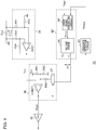
- Fig. 6 is a circuit diagram showing a more specific configuration of the frequency detection circuit 40 and the threshold voltage adjustment circuit 42.
- the peak hold circuit 56 includes transistors Q71 and Q72, resistors R71 and R72, and a capacitor C71. It should be noted that the configuration of the peak hold circuit 56 is not restricted to such an arrangement.
- the error signal generating circuit 44 includes a second comparator COMP2 and a low-pass filter 50.
- the second comparator COMP2 generates a pulse signal S12 that indicates a comparison result between the frequency detection signal V FREQ and the reference value V REF .
- the low-pass filter 50 smoothes the output signal S12 of the second comparator COMP2.
- the low-pass filter 50 includes resistors R81 and R82 and a capacitor C81. However, the configuration of the low-pass filter 50 is not restricted in particular.
- the error signal generating circuit 44 may be an error amplifier configured as an operational amplifier.
- the error signal generating circuit 44 may be an error amplifier including a transconductance amplifier that generates a current that corresponds to a difference between the frequency detection signal V FREQ and the reference value V REF , and a capacitor that smoothes the output current of the transconductance amplifier and converts the smoothed output current into a voltage.
- the voltage source 46 includes a first resistor R21, a second resistor R22, a first transistor M21, and an operational amplifier OA1.
- the first transistor M21 is arranged between the first terminal P1 and the second terminal P2.
- the output of the operational amplifier OA1 is coupled to a control terminal (gate) of the first transistor.
- the frequency error signal V ERR is input to one input terminal (non-inverting input terminal) of the operational amplifier OA1, and the other input terminal (inverting input terminal) is coupled to the second terminal P2.
- the operational amplifier OA1, the first transistor M21, and the second resistor R22 can be regarded as a current source that generates the current I C that corresponds to the frequency error signal V ERR , which corresponds to the current source 48 shown in Fig. 5 .
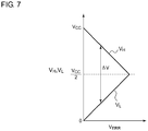
- the upper voltage V H and the lower voltage V L are represented by the following Expressions.
- Fig. 7 is a diagram showing the upper voltage V H and the lower voltage V L .
- the above is the configuration of the lighting circuit 20 according to the first embodiment. Next, description will be made regarding the operation thereof.
- this arrangement is capable of maintaining the average level of the upper threshold signal V THH and the lower threshold signal V THL at a constant level. This is capable of preventing the occurrence of flicker in the semiconductor light source 10.
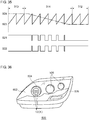
- Figs. 8A through 8C are operation waveform diagrams each showing the operation of the lighting circuit 20.
- Figs. 8A through 8C show operation waveforms with different input voltages V IN .
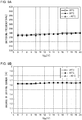
- Fig. 9A is a diagram showing the relation between the input voltage V IN and the switching frequency.
- Fig. 9B is a diagram showing the relation between the input voltage V IN and an average value of the driving current I DRV .
- the frequency feedback control operation functions as an effective measure against fluctuation in the switching frequency due to all kinds of fluctuation and variation such as fluctuation of the output voltage V OUT , variation in the inductance of the inductor L1, and fluctuation in the temperature, in addition to fluctuation of the input voltage V IN .
- This is capable of suppressing unexpected fluctuation in the switching frequency. This allows the costs required for a measure against switching noise to be reduced.
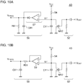
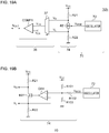
- Figs. 10A and 10B are circuit diagrams each showing the frequency detection circuit 40 according to the first modification.
- the peak hold circuit 56 has a configuration that differs from that shown in Fig. 6 .
- the peak hold circuit 56 includes a capacitor C81, a resistor R81, and a buffer 57.
- the buffer 57 is capable of functioning as a current source. However, the buffer 57 is not capable of functioning as a current sink.
- a peak voltage of the first periodic signal S11 occurs at the capacitor C81.
- the frequency detection circuit 40 shown in Fig. 10B includes an averaging circuit 58 instead of the peak hold circuit 56.
- the averaging circuit 58 includes a buffer 59, a resistor R91, and a capacitor C91, for example.
- the resistor 91 and the capacitor C91 function as a low-pass filter, which averages the output of the buffer 59.
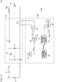
- Fig. 11 is a block diagram showing a lighting circuit 20a according to a second modification.
- a converter controller 32a shown in Fig. 11 further includes a modulator 60 in addition to the converter controller 32 shown in Fig. 3 .
- the modulator 60 superimposes a modulation signal V MOD having a frequency that is lower than the switching frequency of the switching transistor M1 on the reference value V REF that provides the target value of the switching frequency.
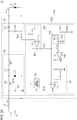
- Fig. 12 is a circuit diagram showing an example configuration of the modulator 60.
- the modulator 60 includes an oscillator 62 that generates the modulation signal V MOD having a frequency that is sufficiently lower than the switching frequency.
- the modulator 60 changes the reference value V REF according to the modulation signal V MOD .
- the oscillator 62 includes resistors R91 through R94, a capacitor C91, and an operational amplifier OA91.
- a triangle-wave modulation signal V MOD occurs at the capacitor C91 with the voltage level determined by the resistors R91 and R92 as a reference voltage.
- the waveform of the modulation signal V MOD is not restricted in particular.
- the modulation signal V MOD may be designed to be any one from among a sawtooth wave, a ramp wave, a sine wave, and a trapezoidal wave.
- the modulation signal V MOD may preferably be configured as a periodic signal having a slope.
- the modulation signal V MOD and the power supply voltage V CC are subjected to weighted averaging (weighted addition) by means of the resistors R95 through R97, thereby generating the reference value V REF on which the modulation signal V MOD has been superimposed.
- the switching frequency is feedback controlled such that the actual switching frequency approaches the target frequency, while slowly changing the target frequency of the switching frequency according to the modulation signal V MOD .
- This arrangement is capable of removing the effects of fluctuation of the input voltage V IN or the output voltage V OUT , variation in the inductance, fluctuation in the temperature, etc., and of providing the switching frequency with a sufficiently wide spectrum. This arrangement is capable of suppressing the occurrence of beat noise, etc.
- the modulator 60 may preferably modulate the difference ⁇ V between the upper threshold signal V THH and the lower threshold signal V THL according to the modulation signal V MOD .
- the modulator 60 may superimpose the modulation signal V MOD on the frequency error signal V ERR , which is an input signal of the operational amplifier OA1.
- the modulator 60 may superimpose the modulation signal V MOD on the gate signal of the first transistor M21, which is an output signal of the operation amplifier OA1.
- Fig. 13 is a circuit diagram showing another example configuration of a part of the lighting circuit 20a according to the second modification.
- the modulation signal V MOD is superimposed on the reference voltage V REF supplied to the input terminal (inverting input terminal) of the second comparator COMP2.
- the frequency detection circuit 40 and the threshold voltage adjustment circuit 42 are each configured as an analog circuit.
- at least a part thereof may be configured as a digital circuit.
- the frequency detection circuit 40 may be configured as a digital counter that measures the period (frequency) of the control pulse S CNT .
- the frequency detection signal is generated as a digital value.
- the threshold voltage adjustment circuit 42 may be configured as a digital circuit.
- the error signal generating circuit 44 may be configured as a compensator that performs a PI (Proportional Integral) control operation or a PID (Proportional Integral Derivative) control operation.
- the voltage source 46 may be configured as a D/A converter or the like.
- the overall configuration of the converter controller 32 may be configured based on a digital circuit.
- an A/D converter that converts the output signal of the current detection circuit 34 into a digital value may preferably be provided as an additional component, and the hysteresis comparator 36 may be configured as a digital comparator.
- the switching converter 30 may be configured as a step-up converter, a step-up/step-down converter, or otherwise a converter employing a transformer. Also, the switching converter 30 may be configured as other kinds of converters such as a Cuk converter or the like.
- Figs. 14A and 14B are circuit diagrams each showing the hysteresis comparator 36 according to a modification.
- the hysteresis comparators shown in Figs. 14A and 14B each include resistors R1 through R3 in addition to the first comparator COMP1.
- the threshold voltage V TH is provided with hysteresis by means of the feedback control operation.
- the feedback amount is changed by changing the resistance value of the feedback resistor R3, so as to change the voltage difference between the threshold voltages V THH and V THL .
- a variable voltage source VS is provided to a feedback path, and the voltage generated by the variable voltage source VS is changed so as to change the voltage difference between the threshold voltages V THH and V THL .
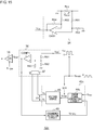
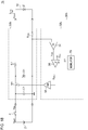
- Fig. 15 is a circuit diagram showing a converter controller 32c according to a sixth modification.
- the converter controller 32c receives a pulse-width modulated PWM dimming signal, and has a PWM dimming (PWM illumination reducing) function of changing the light amount output from the light source according to the duty ratio of the PWM dimming signal.
- the PWM dimming signal S PWM has a frequency on the order of several hundred Hz.
- the converter controller 32 switches on and off the switching transistor M1 according to the control pulse S CNT (operating period).
- the switching transistor M1 is turned off (suspension period).
- PWM pulse width modulation
- PFM pulse frequency modulation
- the configuration for providing the PWM dimming operation is not restricted in particular. For example, as shown in Fig. 15 , the power supply voltage V CC ' supplied to the resistor R61 and/or the power supply voltage V CC ' supplied to the voltage source 46 may be switched between 0 V and V CC according to the PWM dimming signal S PWM .
- the enable state and the disable state of the driver 38 may be controlled according to the PWM dimming signal S PWM .
- the light amount output from the semiconductor light source 10 can be controlled according to the duty ratio of the PWM dimming signal S PWM .
- the control pulse S CNT is fixedly set to the low level (or otherwise the high level). Accordingly, in this state, the switching frequency becomes zero. Accordingly, the frequency detection signal V FREQ detected by the frequency detection circuit 40 becomes a voltage level that corresponds to the zero frequency. In this case, the voltage level of the frequency error signal V ERR deviates from the optimum value for the operating period. As a result, immediately after the PWM dimming signal S PWM transits from the second level (suspension period) to the first level (operating period), the switching frequency of the control pulse S CNT deviates from the target value, following which the switching frequency gradually approaches the target value.
- a threshold voltage adjustment circuit 42c has a function of sampling and holding the frequency error signal V ERR using the PWM dimming signal S PWM .
- Fig. 16 is a circuit diagram showing a specific example configuration of the threshold voltage adjustment circuit 42c shown in Fig. 15 .
- the threshold voltage adjustment circuit 42c further includes a sample-and-hold circuit 90.
- the sample-and-hold circuit 90 receives the PWM dimming signal S PWM in addition to the frequency error signal V ERR .
- the sample-and-hold circuit 90 samples the frequency error signal V ERR , and holds the frequency error signal V ERR thus sampled during the suspension period.
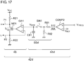
- Fig. 17 is a circuit diagram showing another example configuration of a threshold voltage adjustment circuit 42d shown in Fig. 15 .
- the sample-and-hold circuit 90 shown in Fig. 16 is monolithically configured together with an error signal generating circuit 44d.
- the error signal generating circuit 44d includes a second comparator COMP2 and a low-pass filter 50d.
- a switch SW1 is arranged between a capacitor C81 and a resistor R81 that form the low-pass filter 50d. In the operating period in which the PWM dimming signal S PWM is set to the first level, the switch SW1 is set to the on state. In the suspension period in which the PWM dimming signal S PWM is set to the second level, the switch SW1 is set to the off state.
- the frequency error signal V ERR is maintained at the voltage level set in the operating period even during the suspension period. This allows the switching frequency to immediately approach the target value.
- Fig. 18 is a block diagram showing a vehicular lamp 1b according to a second aspect.
- the converter controller 32b shown in Fig. 18 includes a current detection circuit 34, a hysteresis comparator 36, a driver 38, and a modulator 70.
- the current detection circuit 34 generates a current detection signal V CS that corresponds a driving current I DRV supplied from the switching converter 30 to the semiconductor light source 10.
- the hysteresis comparator 36 compares the current detection signal V CS with the upper threshold signal V THH and the lower threshold signal V THL , and generates a control pulse S CNT that corresponds to the comparison result.
- the driver 38 drives the switching transistor M1 of the switching converter 30 according to the control pulse.
- the modulator 70 generates a modulation signal V MOD having a lower frequency than the switching frequency of the switching transistor M1.
- the modulator 70 modulates the difference between the upper threshold signal V THH and the lower threshold signal V THL according to the modulation signal V MOD .
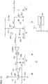
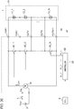
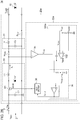
- Figs. 19A and 19B are circuit diagrams each showing a specific example configuration of the converter controller 32b shown in Fig. 18 . Description will be made with reference to Fig. 19A .
- the modulator 70 includes an oscillator 72 and a voltage source 74.
- the oscillator 72 generates a modulation signal V MOD having any one from among a triangle wave, a sawtooth wave, a ramp wave, a sine wave, and a trapezoidal wave.
- the oscillator 72 may have the same configuration as that of the oscillator 62 shown in Fig. 12 . Also, other configurations may be employed.
- the voltage source 74 generates an upper voltage V H and a lower voltage V L , and changes the voltage difference ⁇ V between the upper voltage V H and the lower voltage V L according to the modulation signal V MOD .
- the voltage source 74 may be configured in the same manner as the voltage source 46 shown in Fig. 5 .
- the hysteresis comparator 36 includes a selector 37 and a first comparator COMP1 as with the arrangement shown in Fig. 4 . It should be noted that, in Fig. 19A , the output V TH of the selector 37 is directly input to the first comparator COMP1, and accordingly, the upper voltage V H and the lower voltage V L are employed as the threshold voltages V THH and V THL , respectively. Also, the resistors R61 through R63 may be arranged as additional components as shown in Fig. 4 .
- the voltage source 74 includes resistors R101 through R103, an operational amplifier OA1, a first resistor R21, a second resistor R22, and a first transistor M21.
- the modulation signal V MOD and the power supply voltage V CC are subjected to weighed addition by means of the resistors R101 through R103.
- the operational amplifier OA1, the first transistor M21, and the second resistor R22 correspond to the current source 48 shown in Fig. 19A .
- this arrangement is capable of modulating the difference between the upper voltage V H and the lower voltage V L according to the modulation signal V MOD while maintaining the average of the upper voltage V H and the lower voltage V L at a constant value.
- this arrangement is capable of spreading the spectrum of the switching frequency, thereby suppressing the occurrence of beat noise or the like.
- Fig. 20 is a block diagram showing the vehicular lamp 1 having an ADB function using an array method.
- the high-beam illumination region is formed of N (N represents an integer of 2 or more) multiple divided sub regions.
- the semiconductor light source 10 includes multiple light-emitting elements 12_1 through 12_N associated with the N sub regions.
- Each light-emitting element 12 is configured as a semiconductor device such as an LED (light-emitting diode), LD (laser diode), or the like.
- the light-emitting elements 12 are arranged such that they irradiate the corresponding sub regions.
- the lighting circuit 20 controls the on state (lighting-on state) and the off state (lighting-off state) of each of the multiple light-emitting elements 12_1 through 12_N, so as to change the high-beam light distribution.
- the lighting circuit 20 PWM pulse-width modulation
- the lighting circuit 20 includes multiple bypass circuits 80 1 through 80_N and a controller 82 in addition to the switching controller 30 and the unshown converter controller 32.
- the multiple bypass circuits 80_1 through 80_N are associated with the multiple light-emitting elements 12_1 through 12_N.
- Each bypass circuit 80 is configured to be switchable between the on state and the off state.
- the driving current I DRV flows through the bypass circuit 80_i instead of flowing through the light-emitting element 12_i, which turns off the light-emitting element 12_i.
- the bypass circuit 80_i is set to the off state, the driving current I DRV flows through the light-emitting element 12_i, which turns on the light-emitting element 12_i.
- An upstream processor (e.g., electronic control unit ECU) 6 configured to control the vehicular lamp 1 determines the sub regions to be irradiated by the high-beam based on the state ahead of the vehicle, and instructs the controller 82 of the lighting circuit 20.
- the controller 82 controls the states of the bypass circuits 80_1 through 80_N according to a control instruction received from the processor 6. Specifically, the controller 82 selects the light-emitting elements 12 that correspond to the sub regions to be irradiated, and the bypass circuits 80 respectively arranged in parallel with the light-emitting elements thus selected are set to the off state. Furthermore, the bypass circuits 80 respectively arranged in parallel with the remaining light-emitting elements 12 are turned on.
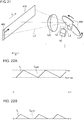
- Fig. 21 is a perspective view showing a schematic configuration of a vehicular lamp 1 having an ADB function employing a blade scanning method.
- the vehicular lamp 1 mainly includes a blade (reflecting mirror) 400, a light source 10, a projector lens 120, and a lighting circuit 20.
- Multiple light sources 10 may be provided.
- description will be made regarding an arrangement including a single light source 10.
- the light source 10 is configured as a semiconductor light source employing an LED (light-emitting diode) or a laser diode.
- the blade 400 receives an output light L1 from the light source 10. Furthermore, the blade 400 repeats a predetermined periodic movement so as to scan a reflected light L2 in a forward region ahead of the vehicle along a horizontal direction (Y direction in the drawing).
- the blade 400 is mounted on a rotor of an unshown motor, and is rotationally driven. At a given time point, the output light L1 input to the blade 400 is reflected with a reflection angle that corresponds to the position (rotational angle of the rotor) of the blade 400, thereby forming an illumination region 402.
- the blade 400 is rotationally driven so as to change the reflection angle, thereby scanning the illumination region 402 in the Y direction.
- the lighting circuit 20 controls the light amount (luminance) to be supplied from the light source 10 in synchronization with the periodic movement of the blade 400 so as to obtain a desired light distribution pattern.
- An area (region) that is provided with the illumination region 402 will be referred to as the "lighting-on region R ON ".
- an area (region) that is not provided with the illumination region 402 will be referred to as the "lighting-off region R OFF ".
- the light distribution pattern 410 is a combination of the lighting-on regions R ON and the lighting-off regions R OFE .
- the configuration for scanning the light ahead of the vehicle is not restricted to such an arrangement shown in Fig. 21 .
- a polygon mirror or a mirror galvanometer may be employed instead of the blade 400.
- a liquid crystal scanner may be employed so as to scan the light.
- the light may be scanned by shifting or displacing a lens in a periodic manner.
- an actuator may be mounted on the light source 10, and the light source 10 itself may be shifted or displaced.
- an optical element (electro-optical element) array that is capable of controlling the light phase may be employed. With such an arrangement, by controlling the wave front of the light, the light traveling direction may be controlled so as to scan the light.
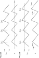
- Figs. 22A and 22B are operation waveform diagrams each showing the operation of the lighting circuit 20r shown in Fig. 1 .
- Fig. 22A shows the operation when the lamp current I LAMP is large.
- Fig. 22B shows the operation when the lamp current I LAMP is small.
- the lamp current I LAMP matches the average value of the peak current and the bottom current. Accordingly, the average level of the lamp current I LAMP , i.e., the luminance, can be linearly controlled according to the reference voltage V ADIM .
- the operation mode becomes a current discontinuous mode, in which the lamp current I LAMP deviates from the average value of the peak value I PEAK and the bottom value I BOTTOM of the coil current I L . Accordingly, the linear luminance control operation cannot be performed according to the reference voltage V ADIM . It should be noted that a similar problem can occur in a case in which the output filter 31 is omitted.
- Fig. 23 is an operation waveform diagram showing the operation of the lighting circuit 20r shown in Fig. 1 .
- a delay time ⁇ OFF ( ⁇ ON ) occurs from the time point at which the detection voltage V CS crosses the threshold signal V THH (V THL ) to the time point at which the switching transistor M1 turns off (turns on) due to the effects of a delay that occurs in the hysteresis comparator 36, a delay that occurs in the driver 38, a delay that occurs in the switching transistor M1, etc.
- the peak value I PEAK of the coil current I L becomes greater than a value I THH that corresponds to the threshold signal V THH , and the bottom value I BOTTOM of the coil current I L becomes smaller than a value I THL that corresponds to the threshold signal V THL .
- I PEAK I THH + ⁇ OFF ⁇ V IN ⁇ V OUT / L 1
- Fig. 24 is a block diagram showing a vehicular lamp 1a according to a third example.
- the vehicular lamp 1a includes a battery 2, a switch 4, a semiconductor light source 10, and a lighting circuit 20a.
- the lighting circuit 20a includes a switching converter 30, an output filter 31, and a converter controller 32a.
- the switching converter 30 is configured as a step-down converter.
- the converter controller 32a stabilizes the lamp current I LAMP , which is supplied from the switching converter 30 to the semiconductor light source 10 via the output filter 31, to a predetermined target current I REF .
- the switching converter 30 may be configured as a step-up converter, a step-up/step-down converter, or otherwise a converter employing a transformer. Also, the switching converter 30 may be configured as other kinds of converters such as a Cuk converter or the like.
- the converter controller 32a includes a current detection circuit 34, a pulse modulator 100, and a driver 38.
- the current detection circuit 34 generates a current detection signal (which will be referred to as the "second current detection signal") V CS2 that corresponds to the coil current (output current) I L of the switching converter 30.
- V CS2 a current detection signal
- a ripple component that occurs in the synchronization of the switching of the switching transistor M1 is superimposed on the second current detection signal V CS2 .
- a sensing resistor R CS may be inserted in series with the inductor L1 on the anode side of the semiconductor light source 10. With such an arrangement, the voltage drop across the sensing resistor R CS may be amplified by means of the current detection circuit 34, so as to generate the second current detection signal V CS2 .
- the configuration of the current detection circuit 34 is not restricted in particular.
- the pulse modulator 100 generates a control pulse S CNT based on the second current detection signal V CS2 .
- the pulse modulator 100 is configured as a controller employing a hysteresis control (Bang-Bang control) method.
- the pulse modulator 100 includes an error amplifier 102 and a low-pass filter 104 in addition to the hysteresis comparator 36.
- the error amplifier 102 amplifies the difference between the DC component of the coil current I L , i.e., the first current signal V CS1 that corresponds to the DC component of the lamp current I LAMP supplied to the semiconductor light source 10, and an analog signal (which will be referred to as the "analog dimming signal” hereafter) V ADIM that indicates the lamp current I LAMP (consequently the luminance) to be supplied, so as to generate an error signal V ERR .
- the first current detection signal V CS1 is configured as a current component obtained by removing a ripple component from the coil current I L . More specifically, the low-pass filter 104 is arranged on the upstream side of the error amplifier 102.
- the low-pass filter 104 smoothes the second current detection signal V CS2 , so as to generate the first current detection signal V CS1 .
- the low-pass filter 104 may be configured as an RC filter.
- the error amplifier 102 amplifies the difference between the first current detection signal V CS1 which is an output of the low-pass filter 104 and the analog dimming signal V ADIM .
- the hysteresis comparator 36 compares the second current detection signal V CS2 with the upper threshold signal V THH and the lower threshold signal V THL determined according to the error signal V ERR , and generates the control pulse S CNT that corresponds to the comparison result.
- the driver 38 drives the switching transistor M1 of the switching converter 30 according to the control pulse S CNT .
- the high level of the control pulse S CNT corresponds to the on state of the switching transistor M1.
- the low level of the control pulse S CNT corresponds to the off state of the switching transistor M1.
- the switching transistor M1 is configured as a P-channel MOSFET.
- the driver 38 applies a low-level voltage (e.g., ground voltage) to the gate of the switching transistor M1.
- the driver 38 applies a high-level voltage (e.g., input voltage V IN ) to the gate of the switching transistor M1.
- Fig. 25A is an operation waveform diagram showing the operation of the lighting circuit 20a shown in Fig. 24 .
- Fig. 25B is an operation waveform diagram showing the operation of a conventional lighting circuit.
- the operation waveforms are shown when the input voltage V IN is small.
- the operation waveforms are shown when the input voltage V IN is large.
- description will be made assuming that ⁇ CN is zero.
- I PEAK I THH + ⁇ OFF ⁇ V IN ⁇ V OUT / L 1
- I THH is also constant. Accordingly, when the input voltage V IN changes, this changes the peak current I PEAK . Accordingly, this leads to a change in the average value of the coil current I L , i.e., leads to a change in the lamp current I LAMP . Specifically, when the input voltage V IN becomes large, this leads to an increase in the slope of V CS in a period in which the coil current I L rises. This also leads to an increase in the peak current I PEAK . Conversely, when the input voltage V IN becomes small, this leads to a reduction in the peak current I PEAK . As a result, I PEAK2 becomes larger than I PEAK1 , and accordingly, I LMAP2 becomes larger than I LAMP1 .
- the error amplifier 102 adjusts the error signal V ERR such that the average value of the current detection signal V CS (i.e., the average value of the coil current I L ) approaches the analog dimming voltage V ADIM , thereby adjusting the threshold signals V THH and V THL .
- V CS the average value of the current detection signal
- V ADIM the analog dimming voltage
- I THH in Expression (1) is adjusted such that the peak current I PEAK is maintained at a constant value.
- the lamp current I LAMP is also maintained at a constant value.
- I THH and I THL are adjusted such that (I PEAK + I BOTTOM )/2 is maintained at a constant value.
- this arrangement is capable of feedback controlling the threshold currents I THH and I THL such that the average current thereof is maintained at a constant value even if the slope of the lamp current I LAMP changes due to a change in the input voltage V IN or the output voltage V OUT . This is capable of solving the fourth problem.
- the threshold signal V THH is adjusted such that the average value of the coil current I L , i.e., the average value of the lamp current I LAMP , is adjusted based on the analog dimming voltage V ADIM .
- this arrangement is capable of solving at least one from among the third problem and the fourth problem.
- the lighting circuit 20a shown in Fig. 24 requires only a single sensing resistor R CS for detecting a current. Accordingly, this arrangement is advantageous from the viewpoint of power loss as compared with a fourth example described later.
- Fig. 26 is a block diagram showing a lighting circuit 20e according to a fourth example.
- the lighting circuit 20e includes a first sensing resistor R CS1 provided on a side closer to the semiconductor light source 10 as compared with the output filter 31, and a second sensing resistor R CS2 provided on a side closer to the inductor L1 as compared with the output filter 31.
- the voltage drop across the first sensing resistor R CS1 is proportional to the lamp current I LAMP (i.e., the DC component of the coil current I L ) smoothed by the output filter 31, which corresponds to the first current detection signal V CS1 .
- the above is the configuration of the lighting circuit 20e according to the fourth example.
- the fourth example provides the same effects as those provided by the third example.
- the first current detection signal V CS1 is affected by detection error in the current detection circuit 34.
- the first current detection signal V CS1 is generated without involving the current detection circuit 34.
- this arrangement is capable of detecting the lamp current I LAMP with high precision without suffering the effects of detection error in the current detection circuit 34.
- Fig. 26 does not require the low-pass filter 104 shown in Fig. 24 . This allows a required cost to be reduced, and allows the circuit area to be reduced.
- the second sensing resistor R CS2 may be inserted on the ground side in the same manner as the sensing resistor R CS shown in Fig. 24 .
- an arrangement may be made in which the first sensing resistor R CS1 is arranged on the anode side of the semiconductor light source 10, and a current detection amplifier is provided as an additional component in order to convert the voltage drop across the first sensing resistor R CS1 into a value with the ground voltage as a reference voltage.
- Fig. 27 is a circuit diagram showing a lighting circuit 20b according to a fifth example.
- the converter controller 32b is configured to be switchable between the hysteresis control mode and an error amplifier control mode based on the output of the error amplifier.
- the converter controller 32b receives, as an input signal from an external circuit, a mode control signal MODE which indicates the mode to be set.
- a mode control signal MODE which indicates the mode to be set.
- PWM pulse width modulation
- the converter controller 32b includes a current detection circuit 34, a driver 38, and a pulse modulator 200.
- the current detection circuit 34 generates a current detection signal V CS that corresponds to the coil current (or output current) I L of the converter 30.
- the pulse modulator 200 generates a control pulse S CNT based on the current detection signal V CS .
- the current detection signal V CS is compared with the threshold signals V THH and V THL , and the control pulse S CNT is output based on the comparison result.
- the pulse modulator 200 adjusts the duty ratio of the control pulse S CNT such that the time average value of the current detection signal V CS approaches a target value thereof.
- the driver 38 drives the switching transistor M1 according to the control pulse S CNT .
- the lighting circuit 20b With the lighting circuit 20b, by selecting a suitable mode according to the operation state of the vehicular lamp, e.g., according to the lamp current (luminance) I LAMP , the input voltage V IN , the output voltage V OUT , etc., this arrangement is capable of solving at least one of the aforementioned problems.
- the hysteresis mode is selected in a situation in which the operation can be performed in the current continuous mode.
- the PWM mode is selected in a situation in which the operation is performed in the current discontinuous mode.
- Fig. 28 is a circuit diagram showing an example configuration of the lighting circuit 20b shown in Fig. 27 .
- the pulse modulator 200 includes a first error amplifier 202, an oscillator 204, a hysteresis voltage source 206, and a comparator unit 208.
- the first error amplifier 202 amplifies the difference between a third current detection signal V CS3 that corresponds to the lamp current I LAMP and a first analog signal V ADIM1 , so as to generate a first error signal V ERR1 .
- the first analog signal V ADIM1 indicates a target value of the lamp current I LAMP to be set in the PWM mode (error amplifier control mode).
- the oscillator 204 generates a periodic signal V OSC having any one from among a triangle wave, a sawtooth wave, and a ramp wave.
- the hysteresis voltage source 206 generates the upper threshold signal V THH and the lower threshold signal V THL determined according to a second analog signal V ADIM2 .
- the second analog signal V ADIM2 indicates a target value of the lamp current I LAMP (coil current I L ) to be set in the hysteresis control mode.
- the comparator unit 208 compares a fourth current detection signal V CS4 that corresponds to the coil current I L with the upper threshold signal V THH and the lower threshold signal V THL , and generates a control pulse S CNT based on the comparison result. Furthermore, in the PWM mode, the comparator unit 208 compares the first error signal V ERR1 with the periodic signal V OSC , and generates the control pulse S CNT based on the comparison result.
- the comparator unit 208 includes a comparator 210, a first selector 212, and a second selector 214.
- the first selector 212 selects one from among the current detection signal V CS and the first error signal V ERR1 according to the mode control signal MODE.
- the second selector 214 selects one from among the threshold signal V THH or otherwise V THL and the periodic signal V OSC according to the mode control signal MODE.
- the high level (1) of the mode control signal MODE corresponds to the PWM mode, and the low level (0) thereof corresponds to the hysteresis control mode.
- the third current detection signal V CS3 and the fourth current detection signal V CS4 are each configured as a current detection signal V CS generated by the current detection circuit 34.
- the present invention is not restricted to such an arrangement.
- the third current detection signal V CS3 and the fourth current detection signal V CS4 may be separately generated by means of different sensing resistors.
- the semiconductor light source 10 is configured as a semiconductor laser.
- the hysteresis control mode is selected.
- the PWM mode is selected.
- the voltage level of the analog dimming signal V ADIM is controlled according to the mode.
- the analog dimming voltage V ADIM is generated by dividing the reference voltage V REF by means of resistors.
- an arrangement may be made in which an upper-side resistor R U of the resistor voltage dividing circuit is configured to have a fixed resistance value, and a lower-side resistor R L thereof is switched according to the mode control signal MODE.
- the lower-side resistor R L may include first resistors R L1 and R L2 and a switch M L2 , and the on/off state of the switch M L2 may be switched according to the mode control signal MODE.
- the mode control signal MODE when the mode control signal MODE is set to 1, the hysteresis control mode is selected. In this mode, the analog dimming signal V ADIM is set to the first analog signal V ADIM1 .
- MODE 0, the PWM mode is selected. In this mode, the analog dimming signal V ADIM is set to the second analog signal V ADIM2 .
- the operation mode is switchable between two modes.
- Fig. 29 is a circuit diagram showing a lighting circuit 20f according to a sixth example.
- the sixth example can be regarded as a combination of the fifth example and the third example.
- a converter controller 32f further includes a second error amplifier 220 and a filter 222 in addition to the configuration of the converter controller 32b shown in Fig. 28 .
- the second error amplifier 220 amplifies the difference between the DC component of the lamp current I LAMP , i.e., a fifth current detection signal V CS5 that corresponds to the DC component of the coil current I L , and a reference signal V ADIM2 that indicates a target value of the fifth current detection signal V CS5 , so as to generate a second error signal V ERR2 .
- the filter 222 corresponds to the low-pass filter 104 shown in Fig. 24 .
- the filter 222 smoothes the current detection signal V CS generated by the current detection circuit 34, so as to generate the fifth current detection signal V CS5 .
- the hysteresis voltage source 206 receives the second error signal V ERR2 instead of the second analog signal V ADIM2 shown in Fig. 28 .
- the hysteresis voltage source 206 generates the upper threshold signal V THH and the lower threshold signal V THL determined according to the second error signal V ERR2 .
- Fig. 30 is a circuit diagram showing a lighting circuit 20g according to a seventh example.
- the seventh example can be regarded as a combination of the fifth example and the fourth example.
- the lighting circuit 20g is provided with two sensing resistors R CS1 and R CS2 in the same manner as the lighting circuit 20e shown in Fig. 26 .
- the fifth current detection signal V CS5 corresponds to the lamp current I LAMP output via the output filter 31 including the inductor L2 and the capacitor C2.
- the other configuration is the same as that shown in Fig. 29 .
- Fig. 31 is a circuit diagram showing a lighting circuit 20c according to an eighth example.
- a pulse modulator 200c further includes a frequency detection circuit 40 and a hysteresis width adjuster 42 in addition to the configuration of the pulse modulator 200 shown in Fig. 28 .
- the frequency detection circuit 40 In the hysteresis control mode, the frequency detection circuit 40 generates a frequency detection signal V FREQ that indicates the frequency of the control pulse S CNT , i.e., the switching frequency of the switching transistor M1.
- the switching frequency can be stabilized to a frequency that corresponds to the reference value V REF regardless of fluctuation of the input voltage V IN or the output voltage V OUT or variation in the inductance L1.
- Fig. 32 is a circuit diagram showing an example configuration of a part of the lighting circuit 20c shown in Fig. 31 .
- the hysteresis voltage source 206 includes resistors R21 and R22, a transistor M21, an operational amplifier OA1, and a selector 37.
- the first resistor R21, the first transistor M21, and the second resistor R22 are sequentially arranged in series between a line 207 at which the analog dimming signal V ADIM is applied and the ground.
- the gate of the first transistor M21 is biased as appropriate.
- an operational amplifier OA1 is provided in order to bias the first transistor M21.
- the output of the operational amplifier OA1 is coupled to the gate of the first transistor M21.
- the non-inverting input terminal of the operational amplifier OA1 is coupled to a connection node that connects the transistor M21 and the second resistor R22.
- a control voltage V X is input to the inverting input terminal thereof.
- the two voltages V H and V L are represented by the following Expressions.
- V H V ADIM ⁇ I X ⁇ R 21
- V L I X ⁇ R 22
- this arrangement is capable of controlling the hysteresis width according to the control voltage V X .
- V H + V L / 2 V ADIM / 2
- this arrangement is capable of controlling the average value of the coil current I according to the analog dimming voltage V ADIM .
- the selector 37 receives the first voltage V H that occurs at a connection node that couples the first resistor R21 and the first transistor M21, and the second voltage V L that occurs at a connection node that couples the first transistor M21 and the second resistor R22.
- the selector 37 outputs one from among the voltages thus received, according to the control pulse S CNT .
- the frequency detection circuit 40 can be regarded as a F/V conversion circuit.
- the frequency detection circuit 40 includes a high-pass filter 52, a first capacitor C11, a second transistor M12, a charger circuit 54, and a peak hold circuit 56.
- the high-pass filter 52 receives the control pulse S CNT or a gate pulse of the switching transistor M1.
- the high-pass filter 52 can also be regarded as a differentiating circuit.
- One end of the first capacitor C11 is grounded.
- the charger circuit 54 charges the first capacitor C11.
- the charger circuit 54 is configured as a current source or otherwise a resistor.
- the transistor M12 is coupled in parallel with the first capacitor C11. When the output signal of the high-pass filter 52 exceeds a gate-source threshold signal, the first capacitor C11 is discharged.
- a first periodic signal S11 having a ramp waveform is generated at the first capacitor C11.
- the frequency detection circuit 40 outputs the frequency detection signal V FREQ that corresponds to the amplitude of the first periodic signal S11.
- the peak hold circuit 56 receives the first periodic signal S11, and outputs the frequency detection signal V FREQ that indicates the peak value of the first periodic signal S11.
- the frequency detection circuit 40 may include a capacitor C12 for holding the peak.
- the hysteresis width adjuster 42 includes a comparator COMP2 and a low-pass filter 50.
- the comparator COMP2 generates a pulse signal S12 that indicates a comparison result between the frequency detection signal V FREQ and a reference value V Y .
- the low-pass filter 50 smoothes the output signal S12 of the comparator COMP2.
- An error amplifier may be substituted for the comparator COMP2 and the low-pass filter 50.
- the oscillator 204 shares circuit components with at least a part of the frequency detection circuit 40 and the hysteresis width adjuster 42.
- the capacitor C12 of the peak hold circuit 56 and the comparator COMP2 of the hysteresis width adjuster 42 are shared as a part of the oscillator 204.
- the oscillator 204 further includes a current source CS1 and a switch SW1 in addition to the comparator COMP2 and the capacitor C12.
- the switch SW1 is arranged in parallel with the capacitor C12.
- the comparator COMP2 compares the voltage V C21 at the capacitor C12 with a predetermined threshold voltage V Y . When V C21 is larger than V Y , the switch SW1 is turned on. With this arrangement, the voltage V C21 across the capacitor C21 is configured as a periodic signal V OSC having a ramp waveform.
- a comparator may be provided in addition to the capacitor C11, the current source 54, and the transistor M12, so as to form the oscillator 204.
- Fig. 33 is a circuit diagram showing a lighting circuit 20h according to a ninth example.
- the lighting circuit 20h is configured as a combination of the lighting circuit 20f shown in Fig. 29 and the lighting circuit 20c shown in Fig. 31 .
- a converter controller 32h shown in Fig. 33 further includes a second error amplifier 220 and a filter 222 in addition to the converter controller 32c shown in Fig. 31 .
- the second error amplifier 220 amplifies the difference between the DC component of the lamp current I LAMP , i.e., the fifth current detection signal V CS5 that corresponds to the DC component of the coil current I L , and a reference signal V ADIM2 that indicates a target value of the fifth current detection signal V CS5 , so as to generate a second error signal V ERR2 .
- the filter 222 smoothes the current detection signal V CS generated by the current detection circuit 34, so as to generate the fifth current detection signal V CS5 .
- the hysteresis voltage source 206 receives the second error signal V ERR2 instead of the second analog signal V ADIM2 shown in Fig. 31 .
- the hysteresis voltage source 206 generates the upper threshold signal V THH and the lower threshold signal V THL , which are shifted up and down according to the second error signal V ERR2 .
- the voltage difference ⁇ V between the upper threshold signal V THH and the lower threshold signal V THL is adjusted by the hysteresis width adjuster 42.
- the fifth current detection signal V CS5 may be generated based on the voltage drop across the sensing resistor R CS1 as shown in Fig. 30 . That is to say, the lighting circuit 20g shown in Fig. 30 and the lighting circuit 20c shown in Fig. 31 may be combined.
- Fig. 34 is a block diagram showing a vehicular lamp 1d according to a tenth example.
- the vehicular lamp 1d includes a first semiconductor light source 10_1 and a second semiconductor light source 10_2 each having one end coupled to a common node, a first switch SW21 arranged in series with the first semiconductor light source 10_1, a second switch SW22 arranged in series with the second semiconductor light source 10_2, and a switching converter 30d that supplies a driving current I DRV to the first semiconductor light source 10_1 and the second semiconductor light source 10_2.
- the switching converter 30d may be configured using a combination of the converters and the controllers described in the first embodiment through the eighth embodiment. However, the configuration of the switching converter 30d is not restricted to such an arrangement.
- the vehicular lamp 1d is configured such that the first switch SW21 and the second switch SW22 are switched on and off according to the PWM dimming pulses S21 and S22 having opposite logical values.
- the PWM controller 300 may include a PWM comparator 302 that compares a PWM ramp wave S23 with a duty instruction value S24 so as to generate the first PWM dimming pulse S21 and an inverter 304 that inverts the first PWM dimming pulse S21 so as to generate the second PWM dimming pulse S22.
- Fig. 35 is an operation waveform diagram showing the operation of the vehicular lamp 1d shown in Fig. 34 .
- this arrangement is capable of turning on one from among the first semiconductor light source 10_1 and the second semiconductor light source 10_2.
- this arrangement is capable of turning on the other one from among the first semiconductor light source 10_1 and the second semiconductor light source 10_2.
- this arrangement is capable of switching the lighting-on state of the first semiconductor light source 10_1 to the lighting-on state of the second semiconductor light source 10_2 in a seamless manner.
- Only a single semiconductor light source 10 is coupled to the output of the single converter 30d over all the periods regardless of the duty ratio. That is to say, only a single semiconductor light source 10 is turned on over all the periods. This allows fluctuation of the output of the switching converter 30d to be reduced, thereby facilitating the design of the switching converter 30d.
- Fig. 36 is a perspective view showing a lamp unit (lamp assembly) 500 including the vehicular lamp 1.
- the lamp unit 500 includes a transparent cover 502, a high-beam unit 504, a low-beam unit 506, and a housing 508.
- the aforementioned vehicular lamp 1 may be employed as the high-beam unit 504, for example.
- the vehicular lamp 1 may be employed as the low-beam unit 506 instead of or otherwise in addition to the high-beam unit 504.
- a bottom-detection and on-time-fixed control operation or otherwise a peak-detection and off-time-fixed control operation may be performed.
- other control operations using an output of the error amplifier such as a PFM control operation may be employed instead of the PWM control operation.
- the present invention is applicable to step-up converters and step-up/step-down converters. It should be noted that, in a case of a step-down converter, the coil current is equivalent to the output current. However, in a case of a step-up converter, the coil current is equivalent to the input current. A part of the coil current corresponds to the output current.
- the present invention is applicable to illumination or the like.
Landscapes
- Engineering & Computer Science (AREA)
- Mechanical Engineering (AREA)
- Power Engineering (AREA)
- Circuit Arrangement For Electric Light Sources In General (AREA)
- Lighting Device Outwards From Vehicle And Optical Signal (AREA)
Claims (9)
- Beleuchtungsschaltung (20), die Folgendes umfasst:einen Schaltwandler (30), der ausgelegt ist, eine Halbleiterlichtquelle (10) mit elektrischer Leistung zu versorgen; undeine Wandlersteuereinrichtung (32), die ausgelegt ist, den Schaltwandler (30) zu steuern,wobei die Wandlersteuereinrichtung (32) Folgendes umfasst:eine Stromdetektionsschaltung (34), die ausgelegt ist, ein Stromdetektionssignal (VCS) zu erzeugen, das einem Antriebsstrom (IDRV) entspricht, der der Halbleiterlichtquelle (10) von dem Schaltwandler (30) zugeführt wird;einen Hysteresekomparator (36), der ausgelegt ist, das Stromdetektionssignal (Vcs) mit einem oberen Schwellensignal (VTHH) und einem unteren Schwellensignal (VTHL) zu vergleichen, um ein Vergleichsergebnis bereitzustellen und um einen Steuerimpuls (SCNT) entsprechend dem Vergleichsergebnis zu erzeugen;einen Treiber (38), der ausgelegt ist, einen Schalttransistor (M1) des Schaltwandlers (30) entsprechend dem Steuerimpuls (SCNT) anzutreiben;eine Frequenzdetektionsschaltung (40), die ausgelegt ist, ein Frequenzdetektionssignal (VFREQ) zu erzeugen, das eine Frequenz des Steuerimpulses (SCNT) anzeigt; undeine Schwellenspannungseinstellschaltung (42), die ausgelegt ist, eine Spannungsdifferenz zwischen dem oberen Schwellensignal (VTHH) und dem unteren Schwellensignal (VTHL) derart zu verändern, dass sich das Frequenzdetektionssignal (VFREQ) einem Referenzwert (VREF) nähert,dadurch gekennzeichnet, dass die Schwellenspannungseinstellschaltung (42) Folgendes umfasst:eine Fehlersignalerzeugungsschaltung (44), die einen Fehlerverstärker umfasst, der als ein Operationsverstärker konfiguriert ist, wobei der Fehlerverstärker ausgelegt ist, eine Differenz zwischen dem Frequenzdetektionssignal (VFREQ) und dem Referenzwert (VREF) zu verstärken, um ein Frequenzfehlersignal (VERR) zu erzeugen, wobei das Frequenzfehlersignal (VERR) desto größer ist, je größer die Differenz (VFREQ - VREF) ist; undeine Spannungsquelle (46), die ausgelegt ist, eine obere Spannung (VH) und eine untere Spannung (VL) zu erzeugen und eine Spannungsdifferenz (VH - VL) zwischen der oberen Spannung (VH) und der unteren Spannung (VL) entsprechend dem Frequenzfehlersignal (VERR) zu verändern, wobei die Spannungsdifferenz (VH - VL) kleiner wird, wenn das Frequenzfehlersignal (VERR) größer wird; undder Hysteresekomparator (36) Folgendes umfasst:eine Auswahlvorrichtung (37), die ausgelegt ist, die obere Spannung (VH) und die untere Spannung (VL) zu empfangen und die obere Spannung (VH) oder die untere Spannung (VL) entsprechend dem Steuerimpuls (SCNT) auszuwählen; undeinen ersten Komparator (COMP1), der ausgelegt ist, das Stromdetektionssignal (Vcs) mit einer Schwellenspannung, die einer Ausgabe der Auswahlvorrichtung (37) entspricht, zu vergleichen;und die obere Schwellenspannung (VTHH) und die untere Schwellenspannung (VTHL) jeweils entsprechend der oberen Spannung (VH) und der unteren Spannung (VL) erzeugt werden.
- Beleuchtungsschaltung nach Anspruch 1, wobei die Spannungsquelle (46) Folgendes umfasst:einen ersten Anschluss zum Ausgeben der oberen Spannung (VH);einen zweiten Anschluss zum Ausgeben der unteren Spannung (VL);einen Transistor (M21), der zwischen den ersten Anschluss und den zweiten Anschluss geschaltet ist;einen ersten Widerstand (R21), der zwischen einer festen Spannungsleitung und dem ersten Anschluss angeordnet ist;einen zweiten Widerstand (R22), der zwischen dem zweiten Anschluss und einer Masseleitung angeordnet ist; undeinen Operationsverstärker (OA1), der einen Ausgang, der mit einem Steueranschluss des Transistors (M21) gekoppelt ist, einen Eingangsanschluss, der gekoppelt ist, um das Frequenzfehlersignal zu empfangen, und den anderen Eingangsanschluss, der an den zweiten Anschluss gekoppelt ist, aufweist.
- Beleuchtungsschaltung nach einem der Ansprüche 1 oder 2, wobei die Frequenzdetektionsschaltung (40) Folgendes umfasst:ein Hochpassfilter (52), das gekoppelt ist, um den Steuerimpuls des Hysteresekomparators (36) oder eines Gate-Impulses des Schalttransistors (M1) zu empfangen;einen ersten Kondensator (C11);eine Ladeschaltung (R54), die ausgelegt ist, den ersten Kondensator zu laden; undeinen zweiten Transistor (M12), der ausgelegt ist, den ersten Kondensator entsprechend einem Ausgangssignal des Hochpassfilters zu entladen,
wobei die Frequenzdetektionsschaltung ausgelegt ist, das Frequenzdetektionssignal entsprechend einer Amplitude eines ersten periodischen Signals, das über dem ersten Kondensator auftritt, auszugeben. - Beleuchtungsschaltung (20a) nach einem der Ansprüche 1 bis 3, die ferner einen Modulator (60) umfasst, der einen Oszillator (62) enthält, der ausgelegt ist, ein Modulationssignal (VMOD) zu erzeugen, das eine niedrigere Frequenz aufweist als eine Schaltfrequenz des Schalttransistors (M1), und eine Spannungsdifferenz zwischen dem oberen Schwellensignal und dem unteren Schwellensignal durch das Verändern des Referenzwertes VREF, der entsprechend dem Modulationssignal in die Schwellenspannungseinstellschaltung (42) eingegeben wird, zu modulieren.
- Beleuchtungsschaltung nach einem der Ansprüche 1 bis 3, die ferner einen Modulator (62) umfasst, der ausgelegt ist, ein Modulationssignal zu erzeugen, das eine niedrigere Frequenz als eine Schaltfrequenz des Schalttransistors besitzt und eine Dreieckswelle, eine Sägezahnwelle, eine Rampenwelle, eine Sinuswelle oder eine Trapezwelle enthält, und das Modulationssignal über den Referenzwert (VREF) zu legen.
- Beleuchtungsschaltung nach Anspruch 1, wobei die Wandlersteuereinrichtung ausgelegt ist, ein Impulsdimmsignal (SPWM) zu empfangen, das entsprechend einer Solllichtmenge für die Halbleiterlichtquelle impulsmoduliert worden ist, und um eine Betriebsperiode, in der der Schalttransistor (M1) ein- und ausgeschaltet wird, und eine Aussetzungsperiode, in der der Schalttransistor ausgesetzt wird, abwechselnd zu wiederholen,
und wobei die Schwellenspannungseinstellschaltung (42) ausgelegt ist, während der Aussetzungsperiode das Frequenzdetektionssignal auf einem Niveau zu halten, das in der unmittelbar vorhergehenden Betriebsperiode eingestellt worden ist. - Beleuchtungsschaltung nach Anspruch 6, wobei die Fehlersignalerzeugungsschaltung (44) Folgendes umfasst:den Fehlerverstärker, der einen zweiten Komparator (COMP2) umfasst, der ausgelegt ist, ein Impulssignal (S12) zu erzeugen, das ein Vergleichsergebnis zwischen einem Frequenzdetektionssignal (VFREQ) und dem Referenzwert (VREF) anzeigt;einen Abtast-/Halte-Kondensator (C81), der ein Ende aufweist, das auf ein festes elektrisches Potenzial eingestellt ist; undeinen Widerstand (R81) und einen Schalter (SW1), die zwischen einem Ausgang des zweiten Komparators (COMP2) und dem anderen Ende des Abtast-/Halte-Kondensators (C81) in Reihe geschaltet sind,wobei der Schalter (SW1) ausgelegt ist, entsprechend dem Impulsdimmsignal (SPWM) ein- und auszuschalten.
- Fahrzeugleuchte (1), die Folgendes umfasst:eine Halbleiterlichtquelle (10); unddie Beleuchtungsschaltung (20) nach einem der Ansprüche 1 bis 7, die ausgelegt ist, die Halbleiterlichtquelle einzuschalten.
- Fahrzeugleuchte (1d), die Folgendes umfasst:eine erste Halbleiterlichtquelle (10_1) und eine zweite Halbleiterlichtquelle (10_2), die jeweils ein Ende aufweisen, das mit einen gemeinsamen Knoten gekoppelt ist;einen ersten Schalter (SW21), der mit der ersten Halbleiterlichtquelle in Reihe angeordnet ist;einen zweiten Schalter (SW22), der mit der zweiten Halbleiterlichtquelle in Reihe angeordnet ist; unddie Beleuchtungsschaltung nach einem der Ansprüche 1 bis 7, die ausgelegt ist, die erste Halbleiterlichtquelle und die zweite Halbleiterlichtquelle mit einem Antriebsstrom zu versorgen,wobei der erste Schalter und der zweite Schalter ausgelegt sind, entsprechend den jeweiligen PWM-Dimmsignalen, die als Logiksignale konfiguriert sind, die einander entgegengesetzt sind, ein- und auszuschalten.
Priority Applications (1)
| Application Number | Priority Date | Filing Date | Title |
|---|---|---|---|
| EP19206884.9A EP3624566B1 (de) | 2015-08-04 | 2016-07-28 | Beleuchtungsschaltung |
Applications Claiming Priority (5)
| Application Number | Priority Date | Filing Date | Title |
|---|---|---|---|
| JP2015154404 | 2015-08-04 | ||
| JP2016021811 | 2016-02-08 | ||
| JP2016052924 | 2016-03-16 | ||
| JP2016115494 | 2016-06-09 | ||
| PCT/JP2016/072203 WO2017022633A1 (ja) | 2015-08-04 | 2016-07-28 | 車両用灯具および光源の点灯回路 |
Related Child Applications (2)
| Application Number | Title | Priority Date | Filing Date |
|---|---|---|---|
| EP19206884.9A Division-Into EP3624566B1 (de) | 2015-08-04 | 2016-07-28 | Beleuchtungsschaltung |
| EP19206884.9A Division EP3624566B1 (de) | 2015-08-04 | 2016-07-28 | Beleuchtungsschaltung |
Publications (3)
| Publication Number | Publication Date |
|---|---|
| EP3334255A1 EP3334255A1 (de) | 2018-06-13 |
| EP3334255A4 EP3334255A4 (de) | 2019-05-15 |
| EP3334255B1 true EP3334255B1 (de) | 2020-11-25 |
Family
ID=57943414
Family Applications (2)
| Application Number | Title | Priority Date | Filing Date |
|---|---|---|---|
| EP19206884.9A Active EP3624566B1 (de) | 2015-08-04 | 2016-07-28 | Beleuchtungsschaltung |
| EP16832912.6A Not-in-force EP3334255B1 (de) | 2015-08-04 | 2016-07-28 | Beleuchtungswerkzeug für fahrzeug und lichtquellenbeleuchtungsschaltung |
Family Applications Before (1)
| Application Number | Title | Priority Date | Filing Date |
|---|---|---|---|
| EP19206884.9A Active EP3624566B1 (de) | 2015-08-04 | 2016-07-28 | Beleuchtungsschaltung |
Country Status (5)
| Country | Link |
|---|---|
| US (1) | US10569695B2 (de) |
| EP (2) | EP3624566B1 (de) |
| JP (1) | JP6726668B2 (de) |
| CN (2) | CN108141940B (de) |
| WO (1) | WO2017022633A1 (de) |
Families Citing this family (25)
| Publication number | Priority date | Publication date | Assignee | Title |
|---|---|---|---|---|
| JP2017070004A (ja) * | 2015-09-28 | 2017-04-06 | ルネサスエレクトロニクス株式会社 | 半導体装置 |
| CN109691235B (zh) * | 2016-09-09 | 2021-02-19 | 株式会社小糸制作所 | 点亮电路、车辆用灯具及光源的驱动方法 |
| US10291124B2 (en) * | 2017-07-06 | 2019-05-14 | Active-Semi (BVI) Inc. | Spread spectrum control apparatus and method |
| CN109640433B (zh) * | 2017-10-05 | 2023-03-31 | 精工爱普生株式会社 | 发光控制电路、光源装置以及投射型影像显示装置 |
| CN107834645A (zh) * | 2017-11-18 | 2018-03-23 | 广西电网有限责任公司电力科学研究院 | 一种应用于配电自动化终端后备超级电容的充电电路 |
| JP6946976B2 (ja) * | 2017-11-28 | 2021-10-13 | 株式会社豊田自動織機 | 誘導性負荷駆動装置 |
| CN111670609B (zh) * | 2018-01-29 | 2022-11-04 | 罗姆股份有限公司 | 发光元件驱动控制装置、发光元件驱动电路装置 |
| CN108832810A (zh) * | 2018-07-10 | 2018-11-16 | 哈尔滨工业大学(深圳) | 二极管伏安特性负载电源的控制方法 |
| CN109193865A (zh) * | 2018-10-29 | 2019-01-11 | 广西电网有限责任公司电力科学研究院 | 一种滞环控制的配电终端超级电容充电电路 |
| CN109617417B (zh) * | 2018-12-12 | 2020-11-17 | 成都芯源系统有限公司 | 一种单功率级多路输出的电源电路及其控制电路 |
| EP3926807A4 (de) | 2019-02-13 | 2022-03-30 | Koito Manufacturing Co., Ltd. | Fahrzeugleuchte, beleuchtungsschaltung dafür und gleichstromwandlersteuerschaltung |
| JP2020155203A (ja) * | 2019-03-18 | 2020-09-24 | セイコーエプソン株式会社 | 発光制御装置、光源装置及び投写型映像表示装置 |
| JP7324056B2 (ja) * | 2019-06-03 | 2023-08-09 | ローム株式会社 | 発光素子駆動装置 |
| CN110225616B (zh) * | 2019-06-06 | 2021-10-15 | 成都芯源系统有限公司 | 调光电路及其控制方法 |
| CN112086855B (zh) * | 2019-06-13 | 2022-11-01 | 海信视像科技股份有限公司 | 激光器驱动电路、激光器显示设备及激光器驱动方法 |
| JP7273749B2 (ja) * | 2020-03-03 | 2023-05-15 | 三菱電機株式会社 | 電源装置及び半導体光源点灯装置 |
| CN111347841B (zh) * | 2020-03-23 | 2022-05-13 | 高斯贝尔数码科技股份有限公司 | 一种汽车消毒灯控制系统及方法 |
| WO2021192368A1 (ja) * | 2020-03-24 | 2021-09-30 | ローム株式会社 | 発光制御装置、発光装置及び車両 |
| JP7534599B2 (ja) * | 2020-05-28 | 2024-08-15 | ミツミ電機株式会社 | 直流電源装置および電源ラインのノイズ抑制方法 |
| US11460873B2 (en) * | 2020-06-09 | 2022-10-04 | Samsung Electronics Co., Ltd. | Power management integrated circuit including detection circuit with capacitive element |
| JP7520668B2 (ja) | 2020-09-30 | 2024-07-23 | ローム株式会社 | 電流検出回路 |
| CN112350573A (zh) * | 2020-11-13 | 2021-02-09 | 福州大学 | 一种Boost-改进升压增益Cuk变换器单开关DC-DC电路 |
| CN118975112A (zh) | 2022-03-31 | 2024-11-15 | 罗姆股份有限公司 | 半导体装置、模块 |
| US20240243547A1 (en) * | 2023-01-13 | 2024-07-18 | Streamlight, Inc. | Driver circuit and method for a semiconductor laser |
| CN119136386B (zh) * | 2024-11-11 | 2025-02-11 | 江苏中科朗恩斯车辆科技有限公司 | 一种可连续调光的光源驱动方法及系统 |
Family Cites Families (28)
| Publication number | Priority date | Publication date | Assignee | Title |
|---|---|---|---|---|
| JP4685531B2 (ja) * | 2005-07-11 | 2011-05-18 | ローム株式会社 | 降圧型スイッチングレギュレータおよびその制御回路ならびにそれを用いた電子機器 |
| US7675487B2 (en) * | 2005-07-15 | 2010-03-09 | Honeywell International, Inc. | Simplified light-emitting diode (LED) hysteretic current controller |
| JP2009542188A (ja) * | 2006-06-26 | 2009-11-26 | コーニンクレッカ フィリップス エレクトロニクス エヌ ヴィ | 負荷を一定電流で駆動する駆動回路 |
| US8237372B2 (en) * | 2006-12-04 | 2012-08-07 | Nxp B.V. | Electronic device for driving light emitting diodes |
| JP2008166165A (ja) * | 2006-12-28 | 2008-07-17 | Toshiba Lighting & Technology Corp | 点灯装置 |
| US7541750B2 (en) * | 2007-05-28 | 2009-06-02 | Leadtrend Technology Corp. | DC to DC converter with load open detection and related method thereof |
| JP5141874B2 (ja) * | 2007-06-28 | 2013-02-13 | 東芝ライテック株式会社 | 照明装置 |
| TWI457049B (zh) * | 2007-07-13 | 2014-10-11 | Richtek Techohnology Corp | 發光二極體驅動器及其控制方法 |
| EP2311298B1 (de) * | 2008-01-30 | 2018-12-19 | Nxp B.V. | Verfahren und schalteranordnung zur regulierung eines durch eine led-schalteranordnung fliessenden led-stroms sowie zugehörige schalterzusammensetzung und beleuchtungssystem |
| JP5291997B2 (ja) | 2008-06-25 | 2013-09-18 | ルネサスエレクトロニクス株式会社 | 超音波モータ制御装置 |
| JP5190390B2 (ja) * | 2009-01-27 | 2013-04-24 | 三菱電機株式会社 | 発光素子点灯制御装置 |
| EP2234255A1 (de) * | 2009-03-27 | 2010-09-29 | Diodes Zetex Semiconductors Limited | Steuerung für Schaltregler, Schaltregler und Lichtquelle |
| JP5407548B2 (ja) * | 2009-05-21 | 2014-02-05 | ミツミ電機株式会社 | スイッチング電源装置 |
| JP5479940B2 (ja) * | 2010-02-16 | 2014-04-23 | 株式会社小糸製作所 | 昇降圧dc−dcコンバータ及び車両用灯具 |
| US20130038234A1 (en) * | 2010-04-30 | 2013-02-14 | Geert Willem Van der Veen | Dimming regulator including programmable hysteretic down-converter for increasing dimming resolution of solid state lighting loads |
| JP2013093214A (ja) * | 2011-10-26 | 2013-05-16 | Koito Mfg Co Ltd | 半導体光源点灯回路 |
| US9265109B2 (en) * | 2012-05-18 | 2016-02-16 | Koito Manufacturing Co., Ltd. | Light source control device |
| JP6030922B2 (ja) * | 2012-06-11 | 2016-11-24 | 株式会社小糸製作所 | 光源制御装置 |
| JP2013258003A (ja) * | 2012-06-12 | 2013-12-26 | Koito Mfg Co Ltd | 半導体光源制御装置 |
| TWI480715B (zh) * | 2012-07-04 | 2015-04-11 | Champion Microelectronic Corp | Led電源驅動功率因素修正器以初級側回授降低電流失真同時控制輸出電流之控制裝置 |
| US8803445B2 (en) * | 2012-09-07 | 2014-08-12 | Infineon Technologies Austria Ag | Circuit and method for driving LEDs |
| CN103199698A (zh) * | 2012-12-14 | 2013-07-10 | 华南理工大学 | Buck-Boost变换器的混杂控制方法 |
| JP6114582B2 (ja) * | 2013-03-14 | 2017-04-12 | 株式会社小糸製作所 | 光源制御装置 |
| JP6147073B2 (ja) * | 2013-04-30 | 2017-06-14 | 株式会社小糸製作所 | 制御部および車両用灯具 |
| JP6262557B2 (ja) * | 2014-02-12 | 2018-01-17 | 株式会社小糸製作所 | 車両用灯具およびその駆動装置、その制御方法 |
| DE102015217712B4 (de) * | 2014-09-16 | 2017-01-19 | Koito Manufacturing Co., Ltd. | Beleuchtungsschaltkreis und Fahrzeugleuchte, die einen solchen aufweist |
| JP6396160B2 (ja) * | 2014-10-02 | 2018-09-26 | 株式会社小糸製作所 | 車両用灯具およびその点灯回路 |
| JP6830774B2 (ja) * | 2016-08-25 | 2021-02-17 | 株式会社小糸製作所 | 点灯回路および車両用灯具 |
-
2016
- 2016-07-28 EP EP19206884.9A patent/EP3624566B1/de active Active
- 2016-07-28 JP JP2017532551A patent/JP6726668B2/ja active Active
- 2016-07-28 CN CN201680045718.XA patent/CN108141940B/zh not_active Expired - Fee Related
- 2016-07-28 EP EP16832912.6A patent/EP3334255B1/de not_active Not-in-force
- 2016-07-28 WO PCT/JP2016/072203 patent/WO2017022633A1/ja not_active Ceased
- 2016-07-28 CN CN201910733838.4A patent/CN110430637B/zh not_active Expired - Fee Related
-
2018
- 2018-02-04 US US15/888,027 patent/US10569695B2/en active Active
Non-Patent Citations (1)
| Title |
|---|
| None * |
Also Published As
| Publication number | Publication date |
|---|---|
| EP3624566A1 (de) | 2020-03-18 |
| JPWO2017022633A1 (ja) | 2018-05-24 |
| CN108141940B (zh) | 2019-11-19 |
| WO2017022633A1 (ja) | 2017-02-09 |
| CN110430637A (zh) | 2019-11-08 |
| EP3334255A1 (de) | 2018-06-13 |
| JP6726668B2 (ja) | 2020-07-22 |
| EP3334255A4 (de) | 2019-05-15 |
| US20180178710A1 (en) | 2018-06-28 |
| EP3624566B1 (de) | 2021-04-07 |
| CN110430637B (zh) | 2022-03-01 |
| US10569695B2 (en) | 2020-02-25 |
| CN108141940A (zh) | 2018-06-08 |
Similar Documents
| Publication | Publication Date | Title |
|---|---|---|
| EP3334255B1 (de) | Beleuchtungswerkzeug für fahrzeug und lichtquellenbeleuchtungsschaltung | |
| US10710495B2 (en) | Automotive lamp | |
| CN107787084B (zh) | 点灯电路以及车辆用灯具 | |
| US10641454B2 (en) | Vehicle lamp that projects scanning beam scanned by optical scanning system to form first pattern, and that projects emission beam of second light source section to form second pattern | |
| US10766400B2 (en) | Vehicle lamp and lighting circuit of light source | |
| US20200187327A1 (en) | Lighting circuit and vehicle lamp | |
| JP6521693B2 (ja) | 車両灯具システム | |
| EP3836756A1 (de) | Beleuchtungsschaltung und fahrzeugleuchte | |
| KR20180121378A (ko) | 차량용 등기구 | |
| JP6767860B2 (ja) | コンバータコントローラおよび車両用灯具 | |
| US10993297B2 (en) | Lighting circuit and vehicular lamp | |
| WO2019078127A1 (ja) | 点灯回路および車両用灯具 | |
| US12526906B2 (en) | Lamp | |
| US12139062B2 (en) | Automotive lamp system | |
| WO2021010325A1 (ja) | 点灯回路および車両用灯具 | |
| CN107771413B (zh) | 车辆前灯 | |
| JP2017224497A (ja) | 車両用灯具および光源の点灯回路 |
Legal Events
| Date | Code | Title | Description |
|---|---|---|---|
| STAA | Information on the status of an ep patent application or granted ep patent |
Free format text: STATUS: THE INTERNATIONAL PUBLICATION HAS BEEN MADE |
|
| PUAI | Public reference made under article 153(3) epc to a published international application that has entered the european phase |
Free format text: ORIGINAL CODE: 0009012 |
|
| STAA | Information on the status of an ep patent application or granted ep patent |
Free format text: STATUS: REQUEST FOR EXAMINATION WAS MADE |
|
| 17P | Request for examination filed |
Effective date: 20180219 |
|
| AK | Designated contracting states |
Kind code of ref document: A1 Designated state(s): AL AT BE BG CH CY CZ DE DK EE ES FI FR GB GR HR HU IE IS IT LI LT LU LV MC MK MT NL NO PL PT RO RS SE SI SK SM TR |
|
| AX | Request for extension of the european patent |
Extension state: BA ME |
|
| DAV | Request for validation of the european patent (deleted) | ||
| DAX | Request for extension of the european patent (deleted) | ||
| RIC1 | Information provided on ipc code assigned before grant |
Ipc: B60Q 1/14 20060101ALI20190212BHEP Ipc: H05B 37/02 20060101AFI20190212BHEP Ipc: H05B 33/08 20060101ALI20190212BHEP Ipc: H02M 3/155 20060101ALI20190212BHEP Ipc: B60Q 1/04 20060101ALI20190212BHEP |
|
| A4 | Supplementary search report drawn up and despatched |
Effective date: 20190417 |
|
| RIC1 | Information provided on ipc code assigned before grant |
Ipc: B60Q 1/14 20060101ALI20190411BHEP Ipc: H02M 3/155 20060101ALI20190411BHEP Ipc: H05B 37/02 20060101AFI20190411BHEP Ipc: H05B 33/08 20060101ALI20190411BHEP Ipc: B60Q 1/04 20060101ALI20190411BHEP |
|
| STAA | Information on the status of an ep patent application or granted ep patent |
Free format text: STATUS: EXAMINATION IS IN PROGRESS |
|
| 17Q | First examination report despatched |
Effective date: 20200124 |
|
| REG | Reference to a national code |
Ref country code: DE Ref legal event code: R079 Ref document number: 602016048743 Country of ref document: DE Free format text: PREVIOUS MAIN CLASS: H05B0037020000 Ipc: H05B0045370000 |
|
| GRAP | Despatch of communication of intention to grant a patent |
Free format text: ORIGINAL CODE: EPIDOSNIGR1 |
|
| STAA | Information on the status of an ep patent application or granted ep patent |
Free format text: STATUS: GRANT OF PATENT IS INTENDED |
|
| RIC1 | Information provided on ipc code assigned before grant |
Ipc: B60Q 1/04 20060101ALI20200728BHEP Ipc: H05B 45/48 20200101ALI20200728BHEP Ipc: H05B 45/37 20200101AFI20200728BHEP Ipc: H02M 3/155 20060101ALI20200728BHEP Ipc: B60Q 1/14 20060101ALI20200728BHEP |
|
| INTG | Intention to grant announced |
Effective date: 20200901 |
|
| RIN1 | Information on inventor provided before grant (corrected) |
Inventor name: KIKUCHI, SATOSHI Inventor name: ICHIKAWA, TOMOYUKI |
|
| GRAS | Grant fee paid |
Free format text: ORIGINAL CODE: EPIDOSNIGR3 |
|
| GRAA | (expected) grant |
Free format text: ORIGINAL CODE: 0009210 |
|
| STAA | Information on the status of an ep patent application or granted ep patent |
Free format text: STATUS: THE PATENT HAS BEEN GRANTED |
|
| AK | Designated contracting states |
Kind code of ref document: B1 Designated state(s): AL AT BE BG CH CY CZ DE DK EE ES FI FR GB GR HR HU IE IS IT LI LT LU LV MC MK MT NL NO PL PT RO RS SE SI SK SM TR |
|
| REG | Reference to a national code |
Ref country code: GB Ref legal event code: FG4D |
|
| REG | Reference to a national code |
Ref country code: CH Ref legal event code: EP |
|
| REG | Reference to a national code |
Ref country code: AT Ref legal event code: REF Ref document number: 1339805 Country of ref document: AT Kind code of ref document: T Effective date: 20201215 |
|
| REG | Reference to a national code |
Ref country code: DE Ref legal event code: R096 Ref document number: 602016048743 Country of ref document: DE |
|
| REG | Reference to a national code |
Ref country code: IE Ref legal event code: FG4D |
|
| REG | Reference to a national code |
Ref country code: AT Ref legal event code: MK05 Ref document number: 1339805 Country of ref document: AT Kind code of ref document: T Effective date: 20201125 |
|
| REG | Reference to a national code |
Ref country code: NL Ref legal event code: MP Effective date: 20201125 |
|
| PG25 | Lapsed in a contracting state [announced via postgrant information from national office to epo] |
Ref country code: GR Free format text: LAPSE BECAUSE OF FAILURE TO SUBMIT A TRANSLATION OF THE DESCRIPTION OR TO PAY THE FEE WITHIN THE PRESCRIBED TIME-LIMIT Effective date: 20210226 Ref country code: FI Free format text: LAPSE BECAUSE OF FAILURE TO SUBMIT A TRANSLATION OF THE DESCRIPTION OR TO PAY THE FEE WITHIN THE PRESCRIBED TIME-LIMIT Effective date: 20201125 Ref country code: NO Free format text: LAPSE BECAUSE OF FAILURE TO SUBMIT A TRANSLATION OF THE DESCRIPTION OR TO PAY THE FEE WITHIN THE PRESCRIBED TIME-LIMIT Effective date: 20210225 Ref country code: PT Free format text: LAPSE BECAUSE OF FAILURE TO SUBMIT A TRANSLATION OF THE DESCRIPTION OR TO PAY THE FEE WITHIN THE PRESCRIBED TIME-LIMIT Effective date: 20210325 Ref country code: RS Free format text: LAPSE BECAUSE OF FAILURE TO SUBMIT A TRANSLATION OF THE DESCRIPTION OR TO PAY THE FEE WITHIN THE PRESCRIBED TIME-LIMIT Effective date: 20201125 |
|
| PG25 | Lapsed in a contracting state [announced via postgrant information from national office to epo] |
Ref country code: AT Free format text: LAPSE BECAUSE OF FAILURE TO SUBMIT A TRANSLATION OF THE DESCRIPTION OR TO PAY THE FEE WITHIN THE PRESCRIBED TIME-LIMIT Effective date: 20201125 Ref country code: LV Free format text: LAPSE BECAUSE OF FAILURE TO SUBMIT A TRANSLATION OF THE DESCRIPTION OR TO PAY THE FEE WITHIN THE PRESCRIBED TIME-LIMIT Effective date: 20201125 Ref country code: IS Free format text: LAPSE BECAUSE OF FAILURE TO SUBMIT A TRANSLATION OF THE DESCRIPTION OR TO PAY THE FEE WITHIN THE PRESCRIBED TIME-LIMIT Effective date: 20210325 Ref country code: PL Free format text: LAPSE BECAUSE OF FAILURE TO SUBMIT A TRANSLATION OF THE DESCRIPTION OR TO PAY THE FEE WITHIN THE PRESCRIBED TIME-LIMIT Effective date: 20201125 Ref country code: BG Free format text: LAPSE BECAUSE OF FAILURE TO SUBMIT A TRANSLATION OF THE DESCRIPTION OR TO PAY THE FEE WITHIN THE PRESCRIBED TIME-LIMIT Effective date: 20210225 Ref country code: SE Free format text: LAPSE BECAUSE OF FAILURE TO SUBMIT A TRANSLATION OF THE DESCRIPTION OR TO PAY THE FEE WITHIN THE PRESCRIBED TIME-LIMIT Effective date: 20201125 |
|
| REG | Reference to a national code |
Ref country code: LT Ref legal event code: MG9D |
|
| PG25 | Lapsed in a contracting state [announced via postgrant information from national office to epo] |
Ref country code: HR Free format text: LAPSE BECAUSE OF FAILURE TO SUBMIT A TRANSLATION OF THE DESCRIPTION OR TO PAY THE FEE WITHIN THE PRESCRIBED TIME-LIMIT Effective date: 20201125 |
|
| PG25 | Lapsed in a contracting state [announced via postgrant information from national office to epo] |
Ref country code: SK Free format text: LAPSE BECAUSE OF FAILURE TO SUBMIT A TRANSLATION OF THE DESCRIPTION OR TO PAY THE FEE WITHIN THE PRESCRIBED TIME-LIMIT Effective date: 20201125 Ref country code: RO Free format text: LAPSE BECAUSE OF FAILURE TO SUBMIT A TRANSLATION OF THE DESCRIPTION OR TO PAY THE FEE WITHIN THE PRESCRIBED TIME-LIMIT Effective date: 20201125 Ref country code: LT Free format text: LAPSE BECAUSE OF FAILURE TO SUBMIT A TRANSLATION OF THE DESCRIPTION OR TO PAY THE FEE WITHIN THE PRESCRIBED TIME-LIMIT Effective date: 20201125 Ref country code: SM Free format text: LAPSE BECAUSE OF FAILURE TO SUBMIT A TRANSLATION OF THE DESCRIPTION OR TO PAY THE FEE WITHIN THE PRESCRIBED TIME-LIMIT Effective date: 20201125 Ref country code: CZ Free format text: LAPSE BECAUSE OF FAILURE TO SUBMIT A TRANSLATION OF THE DESCRIPTION OR TO PAY THE FEE WITHIN THE PRESCRIBED TIME-LIMIT Effective date: 20201125 Ref country code: EE Free format text: LAPSE BECAUSE OF FAILURE TO SUBMIT A TRANSLATION OF THE DESCRIPTION OR TO PAY THE FEE WITHIN THE PRESCRIBED TIME-LIMIT Effective date: 20201125 |
|
| REG | Reference to a national code |
Ref country code: DE Ref legal event code: R097 Ref document number: 602016048743 Country of ref document: DE |
|
| PG25 | Lapsed in a contracting state [announced via postgrant information from national office to epo] |
Ref country code: DK Free format text: LAPSE BECAUSE OF FAILURE TO SUBMIT A TRANSLATION OF THE DESCRIPTION OR TO PAY THE FEE WITHIN THE PRESCRIBED TIME-LIMIT Effective date: 20201125 |
|
| PLBE | No opposition filed within time limit |
Free format text: ORIGINAL CODE: 0009261 |
|
| STAA | Information on the status of an ep patent application or granted ep patent |
Free format text: STATUS: NO OPPOSITION FILED WITHIN TIME LIMIT |
|
| PG25 | Lapsed in a contracting state [announced via postgrant information from national office to epo] |
Ref country code: IT Free format text: LAPSE BECAUSE OF FAILURE TO SUBMIT A TRANSLATION OF THE DESCRIPTION OR TO PAY THE FEE WITHIN THE PRESCRIBED TIME-LIMIT Effective date: 20201125 Ref country code: AL Free format text: LAPSE BECAUSE OF FAILURE TO SUBMIT A TRANSLATION OF THE DESCRIPTION OR TO PAY THE FEE WITHIN THE PRESCRIBED TIME-LIMIT Effective date: 20201125 Ref country code: NL Free format text: LAPSE BECAUSE OF FAILURE TO SUBMIT A TRANSLATION OF THE DESCRIPTION OR TO PAY THE FEE WITHIN THE PRESCRIBED TIME-LIMIT Effective date: 20201125 |
|
| 26N | No opposition filed |
Effective date: 20210826 |
|
| PG25 | Lapsed in a contracting state [announced via postgrant information from national office to epo] |
Ref country code: SI Free format text: LAPSE BECAUSE OF FAILURE TO SUBMIT A TRANSLATION OF THE DESCRIPTION OR TO PAY THE FEE WITHIN THE PRESCRIBED TIME-LIMIT Effective date: 20201125 |
|
| PG25 | Lapsed in a contracting state [announced via postgrant information from national office to epo] |
Ref country code: ES Free format text: LAPSE BECAUSE OF FAILURE TO SUBMIT A TRANSLATION OF THE DESCRIPTION OR TO PAY THE FEE WITHIN THE PRESCRIBED TIME-LIMIT Effective date: 20201125 |
|
| REG | Reference to a national code |
Ref country code: CH Ref legal event code: PL |
|
| GBPC | Gb: european patent ceased through non-payment of renewal fee |
Effective date: 20210728 |
|
| PG25 | Lapsed in a contracting state [announced via postgrant information from national office to epo] |
Ref country code: MC Free format text: LAPSE BECAUSE OF FAILURE TO SUBMIT A TRANSLATION OF THE DESCRIPTION OR TO PAY THE FEE WITHIN THE PRESCRIBED TIME-LIMIT Effective date: 20201125 |
|
| REG | Reference to a national code |
Ref country code: BE Ref legal event code: MM Effective date: 20210731 |
|
| PG25 | Lapsed in a contracting state [announced via postgrant information from national office to epo] |
Ref country code: LI Free format text: LAPSE BECAUSE OF NON-PAYMENT OF DUE FEES Effective date: 20210731 Ref country code: GB Free format text: LAPSE BECAUSE OF NON-PAYMENT OF DUE FEES Effective date: 20210728 Ref country code: CH Free format text: LAPSE BECAUSE OF NON-PAYMENT OF DUE FEES Effective date: 20210731 |
|
| PG25 | Lapsed in a contracting state [announced via postgrant information from national office to epo] |
Ref country code: IS Free format text: LAPSE BECAUSE OF FAILURE TO SUBMIT A TRANSLATION OF THE DESCRIPTION OR TO PAY THE FEE WITHIN THE PRESCRIBED TIME-LIMIT Effective date: 20210325 Ref country code: LU Free format text: LAPSE BECAUSE OF NON-PAYMENT OF DUE FEES Effective date: 20210728 |
|
| PG25 | Lapsed in a contracting state [announced via postgrant information from national office to epo] |
Ref country code: IE Free format text: LAPSE BECAUSE OF NON-PAYMENT OF DUE FEES Effective date: 20210728 Ref country code: BE Free format text: LAPSE BECAUSE OF NON-PAYMENT OF DUE FEES Effective date: 20210731 |
|
| PG25 | Lapsed in a contracting state [announced via postgrant information from national office to epo] |
Ref country code: HU Free format text: LAPSE BECAUSE OF FAILURE TO SUBMIT A TRANSLATION OF THE DESCRIPTION OR TO PAY THE FEE WITHIN THE PRESCRIBED TIME-LIMIT; INVALID AB INITIO Effective date: 20160728 |
|
| P01 | Opt-out of the competence of the unified patent court (upc) registered |
Effective date: 20230517 |
|
| PG25 | Lapsed in a contracting state [announced via postgrant information from national office to epo] |
Ref country code: CY Free format text: LAPSE BECAUSE OF FAILURE TO SUBMIT A TRANSLATION OF THE DESCRIPTION OR TO PAY THE FEE WITHIN THE PRESCRIBED TIME-LIMIT Effective date: 20201125 |
|
| PGFP | Annual fee paid to national office [announced via postgrant information from national office to epo] |
Ref country code: DE Payment date: 20230531 Year of fee payment: 8 |
|
| PG25 | Lapsed in a contracting state [announced via postgrant information from national office to epo] |
Ref country code: MK Free format text: LAPSE BECAUSE OF FAILURE TO SUBMIT A TRANSLATION OF THE DESCRIPTION OR TO PAY THE FEE WITHIN THE PRESCRIBED TIME-LIMIT Effective date: 20201125 |
|
| PG25 | Lapsed in a contracting state [announced via postgrant information from national office to epo] |
Ref country code: TR Free format text: LAPSE BECAUSE OF FAILURE TO SUBMIT A TRANSLATION OF THE DESCRIPTION OR TO PAY THE FEE WITHIN THE PRESCRIBED TIME-LIMIT Effective date: 20201125 |
|
| PGFP | Annual fee paid to national office [announced via postgrant information from national office to epo] |
Ref country code: FR Payment date: 20240611 Year of fee payment: 9 |
|
| PG25 | Lapsed in a contracting state [announced via postgrant information from national office to epo] |
Ref country code: MT Free format text: LAPSE BECAUSE OF FAILURE TO SUBMIT A TRANSLATION OF THE DESCRIPTION OR TO PAY THE FEE WITHIN THE PRESCRIBED TIME-LIMIT Effective date: 20201125 |
|
| REG | Reference to a national code |
Ref country code: DE Ref legal event code: R119 Ref document number: 602016048743 Country of ref document: DE |
|
| PG25 | Lapsed in a contracting state [announced via postgrant information from national office to epo] |
Ref country code: DE Free format text: LAPSE BECAUSE OF NON-PAYMENT OF DUE FEES Effective date: 20250201 |
|
| PG25 | Lapsed in a contracting state [announced via postgrant information from national office to epo] |
Ref country code: FR Free format text: LAPSE BECAUSE OF NON-PAYMENT OF DUE FEES Effective date: 20250731 |