EP3335012B1 - Unité de commande electronique - Google Patents
Unité de commande electronique Download PDFInfo
- Publication number
- EP3335012B1 EP3335012B1 EP16750689.8A EP16750689A EP3335012B1 EP 3335012 B1 EP3335012 B1 EP 3335012B1 EP 16750689 A EP16750689 A EP 16750689A EP 3335012 B1 EP3335012 B1 EP 3335012B1
- Authority
- EP
- European Patent Office
- Prior art keywords
- control unit
- electronic control
- asic
- frequency
- signal
- Prior art date
- Legal status (The legal status is an assumption and is not a legal conclusion. Google has not performed a legal analysis and makes no representation as to the accuracy of the status listed.)
- Active
Links
Images

Classifications
-
- G—PHYSICS
- G01—MEASURING; TESTING
- G01D—MEASURING NOT SPECIALLY ADAPTED FOR A SPECIFIC VARIABLE; ARRANGEMENTS FOR MEASURING TWO OR MORE VARIABLES NOT COVERED IN A SINGLE OTHER SUBCLASS; TARIFF METERING APPARATUS; MEASURING OR TESTING NOT OTHERWISE PROVIDED FOR
- G01D5/00—Mechanical means for transferring the output of a sensing member; Means for converting the output of a sensing member to another variable where the form or nature of the sensing member does not constrain the means for converting; Transducers not specially adapted for a specific variable
- G01D5/12—Mechanical means for transferring the output of a sensing member; Means for converting the output of a sensing member to another variable where the form or nature of the sensing member does not constrain the means for converting; Transducers not specially adapted for a specific variable using electric or magnetic means
- G01D5/243—Mechanical means for transferring the output of a sensing member; Means for converting the output of a sensing member to another variable where the form or nature of the sensing member does not constrain the means for converting; Transducers not specially adapted for a specific variable using electric or magnetic means influencing the phase or frequency of AC
-
- G—PHYSICS
- G01—MEASURING; TESTING
- G01B—MEASURING LENGTH, THICKNESS OR SIMILAR LINEAR DIMENSIONS; MEASURING ANGLES; MEASURING AREAS; MEASURING IRREGULARITIES OF SURFACES OR CONTOURS
- G01B7/00—Measuring arrangements characterised by the use of electric or magnetic techniques
- G01B7/003—Measuring arrangements characterised by the use of electric or magnetic techniques for measuring position, not involving coordinate determination
-
- G—PHYSICS
- G01—MEASURING; TESTING
- G01B—MEASURING LENGTH, THICKNESS OR SIMILAR LINEAR DIMENSIONS; MEASURING ANGLES; MEASURING AREAS; MEASURING IRREGULARITIES OF SURFACES OR CONTOURS
- G01B7/00—Measuring arrangements characterised by the use of electric or magnetic techniques
- G01B7/02—Measuring arrangements characterised by the use of electric or magnetic techniques for measuring length, width or thickness
-
- G—PHYSICS
- G01—MEASURING; TESTING
- G01R—MEASURING ELECTRIC VARIABLES; MEASURING MAGNETIC VARIABLES
- G01R27/00—Arrangements for measuring resistance, reactance, impedance, or electric characteristics derived therefrom
- G01R27/02—Measuring real or complex resistance, reactance, impedance, or other two-pole characteristics derived therefrom, e.g. time constant
- G01R27/26—Measuring inductance or capacitance; Measuring quality factor, e.g. by using the resonance method; Measuring loss factor; Measuring dielectric constants ; Measuring impedance or related variables
- G01R27/2605—Measuring capacitance
-
- G—PHYSICS
- G01—MEASURING; TESTING
- G01R—MEASURING ELECTRIC VARIABLES; MEASURING MAGNETIC VARIABLES
- G01R27/00—Arrangements for measuring resistance, reactance, impedance, or electric characteristics derived therefrom
- G01R27/02—Measuring real or complex resistance, reactance, impedance, or other two-pole characteristics derived therefrom, e.g. time constant
- G01R27/26—Measuring inductance or capacitance; Measuring quality factor, e.g. by using the resonance method; Measuring loss factor; Measuring dielectric constants ; Measuring impedance or related variables
- G01R27/2611—Measuring inductance
Definitions
- the invention relates to an electronic control unit for a device for measuring a measured variable.
- a device for measuring a measured variable can be an inductive sensor.
- Inductive sensors are typically based on a change in one or more characteristic values of a system of one or more inductive components as a result of a measured variable.
- Such inductive components can be called, for example, coil, winding or inductance.
- Measured variables that cause the characteristic values to change can include position or length, angle, force, pressure or torque.
- a position sensor for the brake pedal of an automobile can be named as an example of an application.
- the CN103278181 discloses an LC resonance sensor.
- the inductive sensor with its variable characteristic value usually the inductance L
- L the inductive sensor with its variable characteristic value
- the oscillator always oscillates with its natural frequency, the most important influencing factor of which is L.
- the measurement of L is thus traced back to a frequency measurement, which can easily be carried out, for example, by counting the periods or zero crossings of the oscillator oscillation.
- lock-in amplifier also phase-sensitive rectifier, synchronous demodulator or carrier frequency amplifier
- the inductive sensor receives a stimulus with a fixed frequency (current or voltage).
- a signal processing circuit measures the other electrical quantity on the impedance (voltage or current).
- the signal processing corresponds to a narrow-band filtering of this variable by the frequency of the stimulus with subsequent determination of the complex amplitude and quotient formation with the stimulus to determine the characteristic value.
- the resonant system has limitations in the design of the inductive system because only one oscillation is possible per oscillator. Several signals can only be obtained with several independent oscillators and inductive systems, which significantly increases the cost of sensors with ratiometric or differential measurement. It also has the inductive system always has frequency dependencies, ie it can only be optimally designed for one frequency; the frequency range of the oscillator is always a compromise. By changing the oscillation frequency, cross-sensitivities can falsify the measurement result because, for example, the inductance L is influenced by another frequency-dependent variable in addition to the sensitivity to the measured variable. Finally, the difference between the maximum and the minimum counter result of the frequency measurement must exceed a minimum value so that the respective requirements with regard to measurement accuracy and resolution are met. Depending on the frequency, this requires a minimum measurement time that may not be available at all.
- the lock-in amplifier works with a constant frequency, but also requires a stimulus with this frequency.
- the frequency of these forced vibrations can be freely selected, but due to the frequency dependence of the inductive system, this is a contradiction to operation in resonance, i.e. with vibrations at the natural frequency. Therefore, the following advantages of resonance cannot be used:
- the inductive system as a resonator operated, already represents a filter in that it can achieve a particularly high amplitude in its natural frequency, which facilitates the measurement. Interference, the frequency of which deviates significantly from this frequency, is suppressed by the filter effect.
- the power requirement of the inductive system to maintain the oscillation is lowest in resonance if all other parameters remain the same. With a given power of the stimulus, a particularly high amplitude is thus possible.
- these two advantages represent the same facts, once from the point of view of the measurement and once from the point of view of the stimulus.
- the invention relates to an electronic control unit for a device for measuring a measured variable.
- the electronic control unit is configured to be connected directly to a parallel resonant circuit which is formed from a first inductance and a capacitance.
- the electronic control unit is configured to excite the parallel resonant circuit in an oscillating manner with an excitation frequency which is derived from a cycle of the electronic control unit.
- the electronic control unit is also configured to be connected directly to at least one measuring inductance, which is designed to sense the measured variable and which is coupled to the first inductance. It is also configured to measure a value on the measurement inductance that indicates the measured variable.
- Such an electronic control unit enables the construction of a device with particularly advantageous properties.
- a device for measuring a measured variable typically has a first inductance. It has a measuring inductance which is designed to sense the measured variable and which is coupled to the first inductance is. It also has a capacitance which is connected to the first inductance to form a parallel resonant circuit.
- the device also has the electronic control unit according to the invention.
- the electronic control unit is connected directly to the parallel resonant circuit and, as described, is configured to excite the parallel resonant circuit in an oscillating manner with an excitation frequency.
- the electronic control unit is directly connected to the measuring inductance and is configured to measure a value on the measuring inductance that indicates the measured variable.
- the measuring inductance can only be measured using an electronic control unit in a resonant circuit. This saves energy because the oscillating circuit oscillates by itself and, as a rule, only lost energy is tracked. So there is a forced oscillation. This allows the advantages of resonance to be used and is free from the above-mentioned limitations of a resonant system.
- the use of an electronic control unit to implement the functions saves costs and simplifies the system.
- the excitation of the resonant circuit can also be referred to as a stimulus.
- the excitation frequency can also be referred to as the stimulus frequency.
- the derivation of a clock can in particular take place by deriving from an internal, but also from an external clock. This means in particular that the excitation frequency is independent of a resonance frequency of the parallel resonant circuit.
- the device can be constructed in such a way that it does not have any amplifiers external to the electronic control unit. This also saves costs.
- the provision of a direct connection excludes a respective amplifier between the electronic control unit and components such as inductance or capacitance or oscillating circuit.
- a respective amplifier can in particular be integrated in the electronic control unit.
- the complementary stimulus is advantageous because it causes an oscillation around the mean value of the supply voltage.
- An amplitude is also half that Supply voltage possible or permissible; Depending on the specification of the microcontroller, also beyond that, for example up to half the supply voltage + 0.5 V.
- the voltages at the port pins are typically no longer square-wave voltages due to the internal resistance of the output stages.
- a stimulus that works on one side with port pins against reference potential or supply voltage typically does not offer any comparable options, because every stimulus (alternating voltage) that is added to these voltages is outside the permissible range even at low amplitudes.
- An electronic control unit can be understood to mean, for example, a microprocessor or a microcontroller.
- a microcontroller is to be understood in particular as a component which, in addition to the functions of a microprocessor, also has read / write memory (RAM), at least one type of read-only memory (ROM, EPROM, EEPROM, Flash, etc.), analog-digital memory.
- RAM read / write memory
- ROM read-only memory
- EPROM EEPROM
- Flash Flash
- ADC analog-digital memory
- Such a component typically does not require an external memory for operation and can run a program without external wiring, take measurements with the ADC and output digital signals via port pins that are determined by software or by the timer modules.
- the microcontroller typically only receives a voltage and clock supply as well as a reset pulse when it is switched on.
- a clock oscillator and a reset logic can also be integrated, so that typically only the supply voltage is supplied from the outside.
- the electronic control unit can also be, for example, an arrangement of a microprocessor with external wiring such as memory and clock supply, an application-specific integrated circuit (ASIC), an programmable logic controller (PLC) or an integrated circuit (IC).
- ASIC application-specific integrated circuit
- PLC programmable logic controller
- IC integrated circuit
- the electronic control unit is designed as an application-specific integrated circuit, ASIC, and / or as an application-specific standard product, ASSP. This allows cost advantages through mass production, which justify a certain development effort.
- An analog-to-digital converter (ADC) of the electronic control unit is typically used for measurement.
- the ADC is connected via a multiplexer to a number of port pins at which the voltage can be measured.
- the number of port pins used as inputs and the sequence in which the inputs are switched through to the ADC can typically be configured.
- the port pins connected to the multiplexer are thus available as inputs for performing several independent measurements.
- An integrated circuit can also be considered or defined as an electronic control unit that contains the circuit functions mentioned above. It is not necessary for the IC to be marketed by the manufacturer as an electronic control unit or for it to be freely available as a standard module. In this sense, an ASIC ("Application Specific Integrated Circuit", in particular one for an IC developed by a customer application), which fulfills all technical criteria, as an electronic control unit.
- ASIC Application Specific Integrated Circuit
- the value indicating the measured variable can typically be used to infer the measured variable, for example the measured variable can be calculated or looked up in a table.
- the electronic control unit is designed so that the parallel resonant circuit is connected to a first port pin and to a second port pin of the electronic control unit.
- the second port pin is cleverly supplied with an excitation signal that is inverted to the first port pin.
- an oscillation of the parallel resonant circuit does not take place around a reference potential, in particular ground, or around the supply voltage, but around half the supply voltage or at least around half the supply voltage. This avoids endangering the electronic control unit or the port pins or their wiring.
- the excitation frequency can in particular be achieved by dividing down or taking over a system clock at the port pin. This allows the provision of a signal clocked with the excitation frequency at the port pin using the common functionality of an electronic control unit.
- the stimulus can in particular be derived from a system clock of an electronic control unit.
- a timer or counter can be used for this. This typically divides the clock rate down to the frequency of the stimulus in an integer ratio.
- the system clock can also be used directly.
- the divided clock is preferably connected to the output stages of two or more port pins, one port pin or a group of port pins being controlled with the clock itself, whereas a second port pin or a second group of port pins is controlled with the inverted clock.
- it may be necessary to use a separate timer for each port pin because each timer can only be connected to a specific port pin without the possibility of branching the timer signal. This fact is usually not a problem because modern control units typically have many timers and usually only a few port pins are required, at least two.
- this frequency can optionally be changed by software when the system is in operation.
- a respective resistor in particular an ohmic resistor, can be connected between a number of the port pins and an inductance, that is to say for example the first inductance or the measuring inductance. Also this should still be understood as a direct connection.
- a current can be limited with the resistor, which avoids damage due to overload.
- the electronic control unit can be designed so that the parallel resonant circuit is connected in parallel to the first port pin to a number of further first port pins which are switched synchronously with the first port pin.
- the electronic control unit can also be designed so that the parallel resonant circuit is connected in parallel to the second port pin to a number of further second port pins which are switched synchronously to the second port pin. In this way, the respective maximum current loads of the port pins can be added, so that overall a higher maximum current can be achieved than when only one port pin is used.
- a synchronous circuit is to be understood in particular to mean that the same potential is basically applied to the respective port pins, that is to say that this is also switched over at the same time.
- the electronic control unit is preferably designed or configured for such a synchronous circuit.
- the voltages on the port pins serve in particular as a stimulus.
- a group of port pins optionally instead of a single port pin, which is supplied with the clock, and a single port pin, which is supplied with the inverted clock.
- a number of port pins that have too low a current-carrying capacity can provide a current that is multiplied by the number by being connected in parallel, as already mentioned above.
- inductive systems can be supplied with a stimulus whose impedance would otherwise be too low.
- the inductive system can have several with stimulus Provide inductivities to be supplied.
- the use of a timer per port pin can optionally also make it possible to supply the individual inductances with stimuli of different frequencies or phases.
- Port pins to which the parallel resonant circuit is connected preferably have a push-pull output stage or a tristate output stage. This can mean in particular that there is a switching element (bipolar or MOS transistor) for a low-resistance connection to the voltages of the two logic levels. Such designs have proven to be advantageous for the present application.
- the excitation frequency differs by a maximum of 25%, preferably a maximum of 20%, particularly preferably a maximum of 15%, even more preferably a maximum of 10% from a resonance frequency of the parallel resonant circuit.
- the electronic control unit can be designed to provide such an excitation frequency. It can be designed to determine the resonance frequency, for example as described below. It can also be designed to provide a defined distance between the excitation frequency and the resonance frequency and / or to prevent equality of the excitation frequency and the resonance frequency. An advantageous excitation is thereby achieved. Operation at resonance frequency is typically not intended, but can normally be tolerated as a borderline case.
- the circuit of the stimulus scales well and can be done without Change the requirements for the electronic control unit or the microcontroller with excitation frequencies from the kHz range to the MHz range, for example preferably from 5 kHz to 5 MHz.
- the electronic control unit or the microcontroller typically only the parameters of the inductive system and the capacitor of the resonant circuit are adjusted.
- the lower limit of 5 kHz has the particular effect that the inductances can be made sufficiently small and have as little influence as possible on the system on which measurements are to be made.
- the upper limit has the particular effect that the parasitic capacitances of the port pins and the connected external network together with the internal resistances of the output stages do not then form any effective low-pass filters. It should be understood, however, that frequencies outside the specified range can also be used, since the maximum tolerable influences always depend on the actual circumstances.
- the upper range e.g. from 500 kHz to 5 MHz, is particularly suitable for many measurement tasks, especially in automobiles.
- the inductive system is then very small and, since the required inductances are only a few microhenries, it can also be integrated compactly and inexpensively on a printed circuit board in the form of planar coils. If the inductive system is implemented in the form of planar coils, a stimulus frequency in the upper range is particularly preferred because otherwise the impedances in the inductive system are typically too small to be accessible for precise measurement without great effort.
- the electronic control unit is preferably designed to measure the measuring inductance when it is connected to a first pole on a port pin of the electronic control unit and a second pole is connected to a potential which is at least approximately the corresponds to half the supply voltage of the electronic control unit.
- At least approximately half the supply voltage can in particular be understood to mean a value which has a deviation of ⁇ 10% or ⁇ 5% from half the supply voltage. Exactly half the supply voltage can also be used. A deviation from this exact value does not lead to a measurement error, but can only worsen the achievable resolution.
- the potential which corresponds at least approximately to half the supply voltage of the electronic control unit, can be generated, for example, by means of a voltage divider.
- the potential which corresponds to at least approximately half the supply voltage of the electronic control unit, can also be generated by means of a smoothing capacitor, the smoothing capacitor having a first pole connected to a reference potential or to the supply voltage, and a second pole of the smoothing capacitor being connected via a resistor is connected to a port pin of the electronic control unit, to which a pulsed signal, in particular a signal with a predeterminable pulse duty factor, is applied.
- the electronic control unit can accordingly be designed to output a pulsed signal, in particular a signal with a predefinable duty cycle, on a port pin in order to generate the potential, which corresponds to at least approximately half the supply voltage of the electronic control unit, by means of the smoothing capacitor.
- the resistor can in particular be designed to achieve a small residual ripple, wherein it preferably has a resistance value of over 100 k ⁇ .
- An RC element can also be used as indicated.
- the capacitor is connected on one side to the supply voltage or reference potential, the other side is connected to a connection of a secondary winding of the measuring transformer.
- the resistor is also connected to this node, the value of which is typically in the range of over 100 k ⁇ .
- the other side of the resistor is connected to a port pin.
- the output stage typically switches between the logic levels and possibly also the high-resistance state of a tristate output stage in a timer-controlled manner in order to keep the capacitor voltage at approximately half the supply voltage.
- the timers of the microcontroller can form a pulse width modulator because then only the pulse width modulation (PWM) ratio has to be set for the correction of parameter changes. A central unit will then do little with this task burdened.
- the resistance value in the RC element should preferably be high so that the voltage at half the supply voltage has only a low residual ripple. Due to the filter effect of the measuring circuit, the effect of the residual ripple can be minimized by keeping the signal frequency, which is to be measured by an analog-to-digital converter (ADC), a sufficient distance from the PWM frequency.
- ADC analog-to-digital converter
- the RC element offers the possibility of further improving the metrological properties of the circuit.
- the residual ripple on the capacitor can be used specifically as a so-called “dither” in order to increase the resolution of the measurement.
- An auxiliary signal of low amplitude (the residual ripple) is added to a useful signal.
- the resolution in the measurement of the useful signal can then be increased by multiple sampling of the sum signal.
- the process is known as "dithering". It should be mentioned that the dithering can also be provided otherwise, for example without an RC element.
- the filter function can also be performed by other passive low-pass filters instead of the simple RC element.
- the electronic control unit is preferably configured to initially charge the smoothing capacitor to at least approximately half the supply voltage when switched on, while port pins to which the parallel resonant circuit is connected have the same logic level, and only then start excitation of the parallel resonant circuit.
- inductors affects both the port pins that generate the stimulus and the port pins that generate the Serve measurement, the risk of overvoltages, which can destroy a microcontroller.
- Measures to protect the microcontroller relate to the steady state. When the system is switched on, however, overvoltages can occur, even if the circuit is set up in such a way that there is no danger in the steady state.
- a switch-on procedure designed for protection is advantageous if the use of protective components specifically for the switch-on process is to be avoided. This is a sequence that can be carried out by the central unit of the electronic control unit or the microcontroller by program. As soon as the steady state has been reached, no additional measures are typically necessary and measurement operation can begin.
- the switch-on procedure preferably begins with the measurement circuit, during which the stimulus remains switched off. All existing RC elements or passive low-pass filters, which are used to generate a voltage of approximately half the supply voltage, are preferably precharged so that they can fulfill their purpose. If the stimulus is activated before approximately half the supply voltage has been reached at the corresponding node, the induced voltages can lead to a violation of the permissible voltage range.
- the fact that the resistance of the RC elements has to be high, as described above has a disruptive effect, because this means that pre-charging can take a long time, which causes an undesirable delay between switching on the supply voltage and the sensor system being ready to measure.
- the two connections of the electronic control unit or the microcontroller that provide the stimulus should have the same logic level so that no current flows through the corresponding inductance.
- the inductance has a very low resistance for direct current and is equivalent to a short circuit that would destroy these connections.
- the high-resistance state of tristate outputs is also advantageous. If the stimulus is finally started, it should preferably be activated almost simultaneously at both connections in order to keep the inevitable short circuit at the first level change of the first connection as short as possible.
- the program should preferably be written in such a way or the electronic control unit should preferably be configured in such a way that the delay between the activation times of the outputs is deterministic in that other activities are blocked, e.g. no interrupt is allowed.
- the electronic control unit preferably has an analog-to-digital converter to acquire a signal generated by the measuring inductance, with its characteristic values, in particular amplitude, phase, real part and / or imaginary part being determined, taking into account aliasing, preferably at the excitation frequency.
- the electronic control unit is advantageously configured to determine a frequency component at an evaluation frequency from a signal detected in the electronic control unit, the evaluation frequency in particular the excitation frequency or an alias of the excitation frequency.
- the selected stimulus frequency is so high that the Nyquist frequency of the ADC is below it even at the maximum possible sampling rate, then undersampling can be used in a targeted manner.
- the signal of the stimulus appears through aliasing at a frequency below the respective Nyquist frequency at the output of the ADC; Aliasing is therefore not a disruption or an exclusion criterion here, but rather desirable.
- the stimulus is an amplitude-modulated carrier, because if the measured variable changes, there is an amplitude modulation (AM) of the stimulus with the measured variable.
- AM amplitude modulation
- the sampling rate for correct functioning of the system according to the invention should preferably be at least four times as high as the bandwidth in the measured variable so that the bands do not overlap in a disruptive manner due to aliasing the AM signal has twice the bandwidth of the signal of the measured variable. Since the signal of the stimulus itself is very narrow-band - the coil current is typically almost sinusoidal due to the addition of the inductive system to the resonant circuit - and the bands for low-frequency measured variables can be made slightly narrow compared to the Nyquist bandwidth of the analog-digital converter (ADC) , no special measures are necessary to prevent undesired overlapping of bands due to aliasing and thus a corruption of the signal.
- ADC analog-digital converter
- the measuring inductance or, in general, the inductances at which the voltages to be measured are tapped are typically low-resistance, noise is not a significant factor Problem. Only the low ohmic resistance of the inductors is a source of noise. For the same reason, broadband interference sources in the vicinity of the sensor must typically have very large amplitudes in order to significantly influence the measurement: the low ohmic resistance is effective for capacitively or inductively coupled ones Sources of interference almost like a short circuit, because almost the entire interference voltage drops across the coupling impedance. In most applications, only narrow-band interferers achieve amplitudes that are relevant for the measuring circuit. Therefore, a narrow-band filtering of the voltages to be measured makes sense.
- Such filtering is typically done digitally, using a series of samples from the ADC to isolate the stimulus frequency in the input frequency mix.
- DFT Discrete Fourier Transformation
- the algorithm of which is executed by a central unit of the electronic control unit or the microcontroller.
- Goertzel filter or Goertzel algorithm which can numerically supply the amount and phase of an individual spectral line of the DFT in a particularly efficient manner, is particularly preferred.
- the frequency of the stimulus that is to say the excitation frequency or that alias frequency that arises from undersampling of the excitation frequency, is preferably to be selected as the frequency of this spectral line.
- the measuring inductance is galvanically coupled to the first inductance.
- the measuring inductance is magnetically coupled to the first inductance.
- the measuring inductance can in particular be coupled to the first inductance by being designed as a measuring transformer. Such designs have proven to be advantageous for typical applications.
- the first inductance, the measuring inductance and / or the capacitance are preferably components with a respective tolerance between 1% and 10%, preferably 1%, or less than 1%.
- the tolerance typically specifies the design-related maximum deviation from a target value.
- correspondingly low tolerances facilitate the design of the device, particularly in the context of mass production, since with a low tolerance the maximum deviation of the resonance frequency of the parallel resonant circuit is correspondingly low.
- the maximum quality can be limited in particular by connecting a resistor in the parallel resonant circuit.
- the maximum deviation is typically specified by the tolerance, that is to say the maximum deviation from the target value already mentioned above, of the respective component.
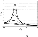
- Figure 1 shows a family of curves which shows the effect of the quality on the benefit of the addition of the inductive system to the resonant circuit in relation to the stimulus, i.e. the excitation by the excitation circuit.
- the ratio of the current I L through the excited inductance to the current I St of the stimulus is plotted. Without the addition of the inductive system to the resonant circuit, this ratio would always be equal to one because there is no further current path. Since the current I L corresponds to the useful current, because it generates the magnetic flux while the current I St corresponds to the effort, the quotient is an evaluation factor for the benefit. Values greater than one correspond to a profit.
- This benefit is plotted against the angular frequency ⁇ normalized to the resonance angular frequency ⁇ 0.
- the flock parameter is the quality; the value at ⁇ 0 in each curve corresponds to the value of the quality, ie the curves represent the quality Q with the values 8; 6; 4; 2; 1; 1 / ⁇ 2 (from top to
- the quality should be as high as possible for the highest possible quality-related benefit
- a high ratio of utility in the middle (resonance) and at the edges of the tolerance range leads to a reduction in usability, which is explained as follows: Every common measuring system, whether analog or digital, has a maximum input amplitude that typically must not be exceeded. Within this maximum, the relative resolution is proportional to the input signal because the smallest distinguishable step of the input signal is constant in the input signal range. If the input signal range is now fully exhausted at resonance, that is off Figure 1 resulting benefits can also be fully utilized. At the edges of the tolerance range, however, the benefit is reduced by the factor which results from the ratio of the benefit in the middle (resonance) and at the edges of the tolerance range.
- the aim is to optimize the design of the sensor system as part of the design.
- the aim is to keep the tolerance of the component parameters L and C, or their geometric mean ⁇ (LC), as low as possible. It is helpful that capacitors with tolerances of 1% and better have become available and cheaper in recent years.
- the main importance for the optimization, however, is the optimal choice of quality. In general, high quality values can typically only be used advantageously in combination with low tolerances of the term ⁇ (LC).
- the design method described below is therefore based on the idea of defining a tolerance for ⁇ (LC) for the respective application based on the availability of suitable, tightly tolerated capacitors and the design of an inductive system, from which the optimal quality can then be calculated.
- Q can also be plotted as a function of ⁇ 0 and ⁇ T.
- Q can be read off directly from such a representation, which saves the repeated insertion of values for Q in the calculation for maximum search.
- the results for Q are always maximum values, ie for a correspondingly designed system with ⁇ 0 and ⁇ T , Q should never exceed the calculated values, because otherwise the input signal range of the measuring system on which it is based is violated. If Q falls below the calculated value, no violation occurs; the input signal range of the measuring system is simply not exhausted.
- the measured variable can be sensed, for example, by changing a position of a magnetic core in the measuring inductance. This can change the value of the inductance of the measurement inductance.
- the measured variable can also be sensed by changing a distance between the measuring inductance and the first inductance.
- the measured variable can be sensed, for example, by changing a position of a magnetic and conductive element, a non-magnetic and conductive element, or a magnetic and non-conductive element adjacent to the measuring inductance and the first inductance.
- the element can for example be arranged between or also next to the first inductance and the measuring inductance. By changing its position, the coupling between the first inductance and the measuring inductance is changed.
- a magnetic and conductive element can be made of steel, for example.
- a non-magnetic and conductive element can be made of aluminum, for example.
- a magnetic and non-conductive element can be made of ferrite, for example.
- the measuring inductance can in particular be designed to sense a measured variable in the form of a position, a length, an angle, a force, a pressure and / or a torque. This corresponds to typical usage scenarios.
- the measured variable can typically be inferred from such characteristic values.
- the device has two, three or more than three measuring inductances or that the electronic control unit is designed for this. These can, for example, be designed to be movable individually or together. In particular, they can be influenced by the same measured variable, so that it is possible to compensate for disturbance variables, in particular the temperature.
- the device can have a first measuring inductance and a second measuring inductance, the first measuring inductance being arranged on a first longitudinal end of the first inductance and the second measuring inductance being arranged on a second longitudinal end of the first inductance.
- Such a design has proven to be advantageous for typical applications.
- the electronic control unit has a direct digital synthesis (DDS) module in order to generate the excitation frequency.
- DDS modules are known in the prior art and allow the almost stepless setting of the excitation frequency at a given cycle. They are typically not part of a microcontroller, but can in particular be used for a specially developed control unit, in particular as an application-specific standard product, or added to a design.
- a DDS module typically allows a much finer setting of the excitation frequency than is possible by dividing a system clock. If, for example, a system clock of 24 MHz is used, an excitation frequency of 4.8 MHz can be achieved with a divider of 5. With the next higher divider of 6, an excitation frequency of 4 MHz can be achieved. In comparison is the excitation frequency adjustable almost continuously using a typical DDS module.
- DDS means “Direct Digital Synthesis” in English and denotes a method known per se which is combined here in an ASIC / ASSP with the inductive sensor system in the manner of a lock-in amplifier and all the features mentioned in this application.
- An oscillator with a fixed frequency is typically used to generate frequencies that can be selected almost at will within a certain interval.
- a register i.e. a memory for a digitally represented number, is typically used, in which the current value of the phase of the signal to be output is stored.
- the value of a further register, the increment register is typically added to the first register, the phase register.
- the value of the phase register increases by a constant value and is therefore proportional to the time.
- phase register The maximum number range that the phase register can represent corresponds to the period of the signal to be output. Therefore, no special measures need to be taken if the phase register overflows; In the selected numerical representation, usually two's complement, the phase values simply assume values increasing again from the most negative value in the next signal period.
- a digital memory for example a ROM
- the address of which is obtained from the phase register is typically connected to the output of the phase register.
- the register bits are directly connected to the address lines of the memory.
- the word length of the phase register comprises significantly more bits than the number of address lines of the memory. This is particularly beneficial.
- the memory is then connected to the most significant address lines.
- the lower-order bits of the phase register allow a particularly precise phase value to be saved.
- the frequency can then be set in particularly narrow increments.
- the memory typically has the task of mapping the waveform of the signal to be output.
- the course of a sinusoid is particularly advantageously stored there. Since the address of the memory is now given by the phase register, it also increases proportionally to the time, the increment register representing the constant of proportionality, i.e. the frequency. There are therefore consecutive data words at the output of the memory which, in the selected numerical representation, correspond to a sine curve, for example.
- the data words are typically fed to a D / A converter whose output, instead of a simple inverter, is connected to the port pin at which the electronic control unit provides the circuit's stimulus.
- One D / A converter is required for each stimulus port pin; if necessary, partial structures of the converters can be used together in order to save silicon area.
- Inverters with staggered current carrying capacity are created in particular by transistors of different sizes (esp Channel width for MOS transistors, emitter area for bipolar transistors).
- D / A converter For maximum simplicity and minimized silicon area of the system, it is possible to intentionally keep certain performance indicators of the combination of DDS and digital-to-analog (D / A) converter at very low values that are otherwise rarely found. Since, for example, the harmonic content at the output of the D / A converter has only a minimal influence on the measurement result (the system typically also works with square-wave stimuli), the word length of the D / A converter can be kept small. In addition, only a single waveform and amplitude must be able to be output. It is therefore not necessary to make the signal values that can be output from the D / A converter equidistant. The D / A converter should only be able to generate the values that are required for this signal shape and amplitude.
- the memory then no longer contains any values that represent a non-linear course in its number range.
- the memory can then be replaced by a combination of counters.
- the circuit with DDS and digital-to-analog converter has two important advantages, both of which are based on the fact that the value of the increment register, which does not change when a signal with a constant frequency is output, is controlled by a higher-level logic unit , which can in particular be integrated in the electronic control unit, can be controlled. This corresponds to frequency modulation (FM) of the stimulus.
- FM frequency modulation
- the system can adjust the resonance frequency of the connected Search for the oscillating circuit during operation. Tolerances of this resonance frequency, whether due to the scattering of manufacturing parameters or influences such as the temperature, become meaningless. Furthermore, at the resonance frequency, the circuit always works at the maximum with regard to the filter effect of the resonant circuit, the spectral purity of the signals, the amplitude of the magnetic field for a given stimulus current and, as a result, with the maximum signal-to-noise ratio.
- the resonant circuit still executes forced oscillations at a fixed, externally specified frequency and does not oscillate freely in resonance. If the quality of the resonant circuit is too high, the microcontroller program can also provide for avoiding the resonance frequency in order to avoid exceeding the input voltage range for the induced voltages on the measuring side.
- the measurement options for inductive systems, the resonance frequency of which can vary greatly during operation due to the measured variable, are also expanded. The program of the microcontroller can then provide for the resonance frequency to be followed in order to achieve a large amplitude of the induced voltages in each case and to use the measured resonance frequency as a measured value or to include it in the calculation.
- Impedance spectroscopy means measuring spectra of the parameters of the inductive system.
- every operation with the resonance frequency means a minimization of the power loss.
- the electronic control unit is configured to determine a resonance frequency of the parallel resonant circuit by changing the excitation frequency. This can be used for various control tasks based on the resonance frequency.
- the electronic control unit can also be designed to set the excitation frequency identical to the resonance frequency or adjacent to the resonance frequency.
- a desired distance for example relative or absolute, can be specified between the excitation frequency and the resonance frequency. This can be positive or negative.
- frequency modulation can be used for interference suppression if either the measurement frequency is constantly changed slightly within a measurement interval, so that each narrow-band interferer actually only interferes in part of the measurement interval, or the microcontroller program searches for frequencies at which a particularly high signal -Noise ratio is found and then remains on this as long as the ratios do not worsen.
- a preferred embodiment is derived from this, in which the electronic control unit is configured to recognize a completed or imminent exceedance of a maximum level at a port pin and to change the excitation frequency in response to this, in particular to distance it further from the resonance frequency of the parallel resonant circuit. This means that it can be exceeded in a simple and reliable manner permissible level with the typical consequences such as measurement errors or damage can be avoided.
- the electronic control unit can be configured to perform interference suppression.
- the excitation frequency can be varied continuously within a measuring interval, for example between a lower frequency and an upper frequency. This allows the elimination of disturbance variables, which are typically only effective in a narrow frequency range, so that the excitation frequency with the variation only sweeps over a frequency of the disturbance variable for a relatively short time.
- the excitation frequency can also be varied within a measurement interval, a signal-to-noise ratio being determined as a function of the excitation frequency.
- the excitation frequency is then set to a value with a maximum signal-to-noise ratio. This allows an automated and simple optimization of the signal-to-noise ratio.
- the electronic control unit has at least one analog multiplier, which is connected to a port pin for connecting the measuring inductance.
- the electronic control unit has a signal module which, according to the invention, is designed as a direct digital synthesis (DDS) module.
- the signal module delivers an oscillating signal at a frequency with a defined, in particular a short distance from the excitation frequency. The distance can be, for example, 5% or 10%.
- An output signal of the analog multiplier is preferably in processed by the electronic control unit to determine the measured variable.
- a function block can be inserted that is typically not included in microcontrollers either.
- This is an analog multiplier as a mixer that can receive the signals from one of the inductances to be measured at one of the inputs, while an oscillation is applied to the other input, which can also be generated by a DDS block as described above.
- This oscillation should have a frequency that differs only by a few percent from the frequency of the stimulus.
- An oscillation then appears at the output of the multiplier, which represents a mixture of signals with the sum and difference frequency.
- This oscillation is passed on to the ADC and processed there in the same way.
- only the difference frequency is advantageously measured from the frequency mixture by setting the digital filtering with DFT or Goertzel filter already described to the difference frequency.
- the frequency of the stimulus and the frequency that the second DDS block outputs are not the same.
- the second DDS block would then typically also be superfluous because the same signal could be used in both cases.
- the difference frequency would be zero if the frequencies are the same, i.e. the voltage output is a direct voltage. This would make digital signal processing easier, because then neither DFT nor Goertzel filters would be necessary, but an oscillation with a difference frequency other than zero can be better isolated by filtering than the DC voltage.
- the information content is higher, because the oscillation is characterized by amplitude, phase and mean value, the DC voltage is only characterized by one value.
- the DDS module is then typically duplicated, whereby a digital-to-analog converter for the second DDS module can be designed with smaller transistors or other circuit principles in order to save chip area, because the output only affects internal nodes of the circuit.
- the device which can be set up by means of the electronic control unit according to the invention, can for example have an oscillator, an optional amplifier, an inductive system, an oscillating circuit capacitor, an optional measuring amplifier and a measuring system, in particular the measuring device.
- the amplifier amplifies the signal of the oscillator; it can be omitted in particular if the output of the oscillator already provides a sufficiently strong signal.
- This signal or that of the amplifier form the stimulus for the inductive system, which is supplemented by the capacitor to form the resonant circuit.
- the first inductance already mentioned above and the measuring inductance likewise already mentioned can be viewed as an inductive system.
- an additional measuring amplifier can be used, otherwise the measuring system in particular can be connected directly to the inductive system, for example by tapping an electrical variable or several electrical variables on the inductive system.
- the measuring system can, for example, be implemented as a lock-in amplifier (or phase-sensitive rectifier, synchronous demodulator or carrier frequency amplifier) implemented in analog or digital technology and possibly software and can determine one or more characteristic values of the inductive system with the aid of the oscillator signal as a reference signal.
- the excitation frequency is preferably adjustable. In particular, it can be set using software. This allows the excitation frequency or the stimulus to be modulated. Alternatively, the excitation frequency can also be fixed.
- the electronic control unit can be designed or configured, in particular, as a lock-in amplifier for the measurement described herein. This can also be referred to as a phase-sensitive rectifier, synchronous demodulator or carrier frequency amplifier and has proven to be advantageous for the application relevant here.
- the described design of an inductive system and a combination of the components described here ensures that the excess of the quantities relevant for the measurement, as is characteristic of resonance, in conjunction with a signal processing path as known from the lock-in amplifier can be connected. This reduces the power requirement of an inductive sensor system and / or increases its measurement resolution.
- Typical values in the range from 3 to 8 can advantageously be used or expected for Vt 2 / V0.
- the invention also relates to a device with an electronic control unit according to the invention. All of the designs and variants described can be used. The device in all variants can in particular also be claimed separately.
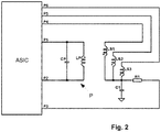
- An inductive system is designed as a measuring transformer made up of a first inductance LP and three measuring inductances, namely a first measuring inductance LS1, a second measuring inductance LS2 and a third measuring inductance LS3.
- a stimulus is provided by port pins P1 and P2 of the ASIC, which are controlled by an internal DDS module with an intended excitation frequency or stimulus frequency.
- a capacitance CP is connected in parallel with the first inductance LP, as a result of which a parallel resonant circuit P results.
- the oscillations of the resonant circuit P are continuously maintained by alternating voltages at P1 and P2, so that an oscillation of constant amplitude results.
- the current through the first inductance LP causes a magnetic flux which also detects the measuring inductances LS1, LS2, LS3.
- the magnetic coupling is symbolized by the arrow.
- the percentage of the magnetic flux of the first inductance LP, which also goes through the measuring inductances LS1, LS2 and LS3, depends on the measured variable.
- the distance between the first inductance LP and the measuring inductances LS1, LS2 and LS3 can change in order to measure it.
- a soft magnetic core or an electrically conductive body could also be located between the first inductance LP and the measuring inductances LS1, LS2 and LS3, the movement of which is measured.
- the magnetic flux induces voltages in the measuring inductances LS1, LS2 and LS3, which are fed to port pins P4, P5, P6 of the ASIC.
- An advantage of using three inductors LS1, LS2 and LS3 instead of a single one is the possibility of gaining more data for measuring the measurand.
- Values of the measuring inductances LS1, LS2 and LS3 therefore depend in different ways on the measured variable, so that any measuring errors in one of the measuring inductances LS1, LS2, LS3 can be corrected by calculating the measured values at all measuring inductances LS1, LS2 and LS3.
- the typically most important disturbance variable namely the temperature, can be compensated for.
- several measured variables can also be recorded with one system.
- the voltages at the port pins P4, P5, P6 are alternately fed to an analog-to-digital converter (ADC) in the ASIC via an integrated multiplexer.
- ADC analog-to-digital converter
- the ADC records each of these voltages several times.
- the amplitude and phase at the stimulus frequency are determined from the plurality of sample values that are determined by the ADC for each voltage. Further steps of digital signal processing and software can be carried out in order to finally determine the measured value for the measured variable from the amplitude and phase values.
- the measuring inductances LS1, LS2, LS3 are connected to a common potential, which is defined by a smoothing capacitor C1, at their respective poles which are opposite the poles connected to the port pins P4, P5, P6.
- the smoothing capacitor C1 is connected to its pole, which defines this potential, via a resistor R1 connected to a port pin P3 of the ASIC.
- the ASIC applies a pulse-width-modulated signal to this port pin P3 in order to maintain a certain potential on the average on the smoothing capacitor C1. This potential corresponds approximately to half the supply voltage of the ASIC.
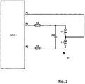
- Figure 3 shows a device according to a second embodiment of the invention.
- An ASIC is also provided here. The differences in the wiring compared to the device according to the first exemplary embodiment are explained below.
- a parallel resonant circuit P is formed by a first inductance L1, a measuring inductance L2 and a capacitance CP.
- the measuring inductance L2 is sensitive to the measured variable and changes, while the first inductance L1 has a constant value.
- resistors R2 and R3 which protect the port pins P1, P2 from excessive currents.
- a voltage is tapped between the first inductance L1 and the measuring inductance L2, which oscillates with the stimulus frequency and whose amplitude and phase depend on the measured variable.
- Figure 4 shows a possible internal circuit at P1 and P2, in particular if a standard port pin of an ASIC or another electronic component in CMOS technology is used.
- An inverter is formed from MOS transistors M1 and M2, the P-MOSFET M1 having the channel width WP and the N-MOSFET M2 having the channel width WN which is suitable for this in the present technology.
- the circuit is controlled by the stimulus signal; its output is connected to the actual port pin P1, the same structure can be found again at P2.
- a supply voltage is labeled VDD, which also applies to other figures.
- FIG Figure 5 One possible embodiment for a digital-to-analog converter is shown in FIG Figure 5 shown.
- the transistors M1 to M6 There are now three inverters with the transistors M1 to M6, the channel widths of the transistors being staggered and assuming the values WP / 2, WP / 4 and WP / 8 or WN / 2, WN / 4 and WN / 8.
- the transistors are not connected as inverters, but are supplied with input signals s1 to s6.
- the stimulus can be generated in 15 impedance or voltage levels and corresponding currents instead of just two levels if the signals s1 to s6 are cyclical like this changed so that all stages are run through.
- the circuit is very efficient with regard to its silicon area, because the area consumption is largely determined by the channel width and the summed channel width of the transistors M1 to M6 is the result Fig. 4 does not exceed. In other words, in both cases the same total channel width is required for the same total current carrying capacity.
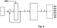
- a circuit for generating the signals s1 to s6 by means of DDS is shown in Fig. 6 shown.
- the outputs of an increment register 1 and a phase register 2 act on an adder, the output of which is connected to the input of the phase register 2.
- OSC oscillator signal
- the value of the phase register is increased by the value of the increment register.
- the content of the increment register is assumed to be a constant and therefore no input for setting this register is shown.
- the output of the phase register 2 is connected to the address bus A of a memory 3, as a result of which certain addresses of the memory 3 are selected.
- the address bus is n bits wide.
- the data words corresponding to the addresses then appear at the output of the memory 3, the data bus D.
- the data bus has a width of 4 bits because the 15 states of the corresponding digital-to-analog converter are off Fig. 5 can be coded with 4 bits.
- the data words of the data bus D are fed to a decoder 4, which converts the signals s1 to s6.
- Each of the 15 options for setting the digital-to-analog converter to a specific output value corresponds to a specific data word with 4 bits and a corresponding combination of signals s1 to s6.
- the combination of the increment register 1, the phase register 2, the adder and the memory 3 is usually called DDS.
Landscapes
- Physics & Mathematics (AREA)
- General Physics & Mathematics (AREA)
- Measurement Of Resistance Or Impedance (AREA)
Claims (14)
- Unité de commande électronique réalisée sous forme d'ASIC, destinée à un dispositif de mesure d'une grandeur de mesure, l'unité de commande électronique (ASIC) étant configurée pour- être reliée directement à un circuit oscillant parallèle (P) qui est formé par une première inductance (LP, L1) et une capacité (CP),- faire osciller le circuit oscillant parallèle (P) à une fréquence d'excitation qui est dérivée d'une cadence d'horloge de l'unité de commande électronique,- être reliée directement à au moins une inductance de mesure (LS1, LS2, LS3, L2) qui est réalisée pour détecter la grandeur de mesure et qui est couplée à la première inductance (LP, L1), et- mesurer une valeur indiquant la grandeur de mesure au niveau de l'inductance de mesure (LS1, LS2, LS3, L2), dans laquelle- l'unité de commande électronique (ASIC) présente un module de synthèse numérique directe (DDS) pour produire la fréquence d'excitation.
- Unité de commande électronique (ASIC) selon la revendication 1, caractérisée en ce que- l'unité de commande électronique est réalisée pour que le circuit oscillant parallèle (P) soit connecté à une première broche de borne et à une deuxième broche de borne de l'unité de commande électronique (ASIC), la deuxième broche de borne étant alimentée par un signal d'excitation inversé par rapport à la première broche de borne.
- Unité de commande électronique (ASIC) selon la revendication 2, caractérisée en ce que- l'unité de commande électronique (ASIC) est réalisée pour que le circuit oscillant parallèle (P)- soit connecté en parallèle à la première broche de borne avec un certain nombre d'autres premières broches de borne qui sont connectées de manière synchrone avec la première broche de borne, et/ou- soit connecté en parallèle à la deuxième broche de borne avec un certain nombre d'autres deuxièmes broches de borne qui sont connectées de manière synchrone avec la deuxième broche de borne.
- Unité de commande électronique (ASIC) selon l'une quelconque des revendications précédentes, caractérisée en ce que- des broches de borne qui sont réalisées pour la connexion du circuit oscillant parallèle (P) présentent un étage de sortie push-pull ou un état de sortie à trois états respectif.
- Unité de commande électronique (ASIC) selon l'une quelconque des revendications précédentes, caractérisée en ce que- l'unité de commande électronique (ASIC) est réalisée sous la forme d'un produit standard spécifique à une application, ASSP.
- Unité de commande électronique (ASIC) selon l'une quelconque des revendications précédentes, caractérisée en ce que- l'unité de commande électronique (ASIC) est réalisée pour mesurer l'inductance de mesure (LS1, LS2, LS3, L2) lorsqu'elle est reliée à un premier pôle sur une broche de borne de l'unité de commande électronique (ASIC) et est reliée à un deuxième pôle ayant un potentiel qui correspond au moins approximativement à la moitié de la tension d'alimentation de l'unité de commande électronique (ASIC).
- Unité de commande électronique (ASIC) selon la revendication 6, caractérisée en ce que- l'unité de commande électronique est réalisée pour sortir à une broche de borne un signal pulsé, en particulier un signal ayant un rapport cyclique prédéfinissable afin de produire le potentiel qui correspond au moins approximativement à la moitié de la tension d'alimentation de l'unité de commande électronique (ASIC) au moyen d'un condensateur de lissage (C1).
- Unité de commande électronique (ASIC) selon la revendication 7, caractérisée en ce que- l'unité de commande électronique (ASIC) est configurée lors de la mise sous tension pour recharger d'abord le condensateur de lissage (C1) au moins approximativement à la moitié de la tension d'alimentation alors que des broches de borne auxquelles est connecté le circuit oscillant parallèle (P) présentent le même niveau logique, et pour commencer seulement ensuite une excitation du circuit oscillant parallèle (P).
- Unité de commande électronique (ASIC) selon l'une quelconque des revendications précédentes, caractérisée en ce que- l'unité de commande électronique (ASIC) présente un convertisseur analogique/numérique pour détecter un signal produit par l'inductance de mesure (LS1, LS2, LS3, L2), et est configurée pour déterminer, en tenant compte d'un crénelage, les valeurs caractéristiques de celui-ci, en particulier l'amplitude, la phase, la partie réelle et/ou la partie imaginaire, de préférence à la fréquence d'excitation.
- Unité de commande électronique (ASIC) selon l'une quelconque des revendications précédentes, caractérisée en ce que- l'unité de commande électronique (ASIC) est configurée pour déterminer une composante de fréquence à partir d'un signal détecté à une fréquence d'évaluation,- la fréquence d'évaluation étant en particulier la fréquence d'excitation ou un alias de la fréquence d'excitation.
- Unité de commande électronique (ASIC) selon l'une quelconque des revendications précédentes, caractérisée en ce que- l'unité de commande électronique (ASIC) est configurée pour établir une fréquence de résonance du circuit oscillant parallèle (P) en faisant varier la fréquence d'excitation, et pour régler la fréquence d'excitation de manière identique à la fréquence de résonance ou proche de la fréquence de résonance.
- Unité de commande électronique (ASIC) selon l'une quelconque des revendications précédentes, caractérisée en ce que- l'unité de commande électronique (ASIC) est configurée pour identifier un dépassement survenu ou imminent d'un niveau maximal à une broche de borne, et pour modifier en réponse à cela la fréquence d'excitation, en particulier pour l'éloigner davantage de la fréquence de résonance du circuit oscillant parallèle (P).
- Unité de commande électronique (ASIC) selon l'une quelconque des revendications précédentes, caractérisée en ce que- l'unité de commande électronique (ASIC) est configurée pour effectuer une suppression des interférences, pour laquelle- la fréquence d'excitation est amenée à varier en continu à l'intérieur d'un intervalle de mesure, et/ou- la fréquence d'excitation est amenée à varier à l'intérieur d'un intervalle de mesure, et en fonction de la fréquence d'excitation un rapport signal/bruit est établi, la fréquence d'excitation étant par la suite réglée sur une valeur ayant un rapport signal/bruit maximal.
- Unité de commande électronique (ASIC) selon l'une quelconque des revendications précédentes, caractérisée en ce que- l'unité de commande électronique (ASIC) présente au moins un multiplicateur analogique qui est connecté à une broche de borne pour connecter l'inductance de mesure,- l'unité de commande électronique présentant un module de signal,- le module de signal fournissant un signal oscillant ayant une fréquence avec une distance définie, en particulier faible, par rapport à la fréquence d'excitation,- le module de signal est réalisé sous la forme d'un module de synthèse numérique directe (DDS),- et un signal de sortie du multiplicateur analogique, en un signal de différence, étant traité ultérieurement dans l'unité de commande électronique (ASIC) pour établir les grandeurs de mesure.
Applications Claiming Priority (2)
| Application Number | Priority Date | Filing Date | Title |
|---|---|---|---|
| DE102015215331.2A DE102015215331A1 (de) | 2015-08-11 | 2015-08-11 | Elektronische Steuerungseinheit |
| PCT/EP2016/068158 WO2017025355A1 (fr) | 2015-08-11 | 2016-07-29 | Unité de commande électronique |
Publications (2)
| Publication Number | Publication Date |
|---|---|
| EP3335012A1 EP3335012A1 (fr) | 2018-06-20 |
| EP3335012B1 true EP3335012B1 (fr) | 2021-06-02 |
Family
ID=56683917
Family Applications (1)
| Application Number | Title | Priority Date | Filing Date |
|---|---|---|---|
| EP16750689.8A Active EP3335012B1 (fr) | 2015-08-11 | 2016-07-29 | Unité de commande electronique |
Country Status (6)
| Country | Link |
|---|---|
| US (1) | US10571307B2 (fr) |
| EP (1) | EP3335012B1 (fr) |
| KR (1) | KR20180040149A (fr) |
| CN (1) | CN108027255B (fr) |
| DE (2) | DE102015215331A1 (fr) |
| WO (1) | WO2017025355A1 (fr) |
Families Citing this family (33)
| Publication number | Priority date | Publication date | Assignee | Title |
|---|---|---|---|---|
| DE102016202403A1 (de) * | 2016-02-17 | 2017-08-17 | Continental Teves Ag & Co. Ohg | Sensor |
| DE102016202402A1 (de) * | 2016-02-17 | 2017-08-17 | Continental Teves Ag & Co. Ohg | Sensor |
| CN106934913A (zh) * | 2017-02-20 | 2017-07-07 | 深圳怡化电脑股份有限公司 | 一种测量电感变化的系统与方法 |
| JP6953865B2 (ja) * | 2017-07-28 | 2021-10-27 | 富士フイルムビジネスイノベーション株式会社 | 情報処理システム |
| US11537242B2 (en) | 2018-03-29 | 2022-12-27 | Cirrus Logic, Inc. | Q-factor enhancement in resonant phase sensing of resistive-inductive-capacitive sensors |
| US12295102B1 (en) | 2018-03-29 | 2025-05-06 | Cirrus Logic Inc. | Far field interference cancellation for resistive-inductive-capacitive sensors |
| US10921159B1 (en) | 2018-03-29 | 2021-02-16 | Cirrus Logic, Inc. | Use of reference sensor in resonant phase sensing system |
| US10908200B2 (en) * | 2018-03-29 | 2021-02-02 | Cirrus Logic, Inc. | Resonant phase sensing of resistive-inductive-capacitive sensors |
| US11092657B2 (en) | 2018-03-29 | 2021-08-17 | Cirrus Logic, Inc. | Compensation of changes in a resonant phase sensing system including a resistive-inductive-capacitive sensor |
| US10642435B2 (en) * | 2018-03-29 | 2020-05-05 | Cirrus Logic, Inc. | False triggering prevention in a resonant phase sensing system |
| US10725549B2 (en) * | 2018-03-29 | 2020-07-28 | Cirrus Logic, Inc. | Efficient detection of human machine interface interaction using a resonant phase sensing system |
| US12130159B2 (en) * | 2018-08-22 | 2024-10-29 | Cirrus Logic Inc. | Detecting and adapting to changes in a resonant phase sensing system having a resistive-inductive-capacitive sensor |
| US11402946B2 (en) | 2019-02-26 | 2022-08-02 | Cirrus Logic, Inc. | Multi-chip synchronization in sensor applications |
| US10948313B2 (en) | 2019-02-26 | 2021-03-16 | Cirrus Logic, Inc. | Spread spectrum sensor scanning using resistive-inductive-capacitive sensors |
| US10935620B2 (en) | 2019-02-26 | 2021-03-02 | Cirrus Logic, Inc. | On-chip resonance detection and transfer function mapping of resistive-inductive-capacitive sensors |
| US11536758B2 (en) | 2019-02-26 | 2022-12-27 | Cirrus Logic, Inc. | Single-capacitor inductive sense systems |
| US11474135B2 (en) * | 2019-04-03 | 2022-10-18 | Cirrus Logic, Inc. | Auto-centering of sensor frequency of a resonant sensor |
| US11079874B2 (en) | 2019-11-19 | 2021-08-03 | Cirrus Logic, Inc. | Virtual button characterization engine |
| US12463643B2 (en) | 2019-11-19 | 2025-11-04 | Cirrus Logic Inc. | Baseline calculation for sensor system |
| US11579030B2 (en) | 2020-06-18 | 2023-02-14 | Cirrus Logic, Inc. | Baseline estimation for sensor system |
| US11868540B2 (en) | 2020-06-25 | 2024-01-09 | Cirrus Logic Inc. | Determination of resonant frequency and quality factor for a sensor system |
| US11835410B2 (en) | 2020-06-25 | 2023-12-05 | Cirrus Logic Inc. | Determination of resonant frequency and quality factor for a sensor system |
| DE102021200913A1 (de) * | 2021-02-02 | 2022-08-04 | Mahle International Gmbh | Elektronische Schaltungsanordnung und Verfahren |
| US11619519B2 (en) | 2021-02-08 | 2023-04-04 | Cirrus Logic, Inc. | Predictive sensor tracking optimization in multi-sensor sensing applications |
| US11808669B2 (en) | 2021-03-29 | 2023-11-07 | Cirrus Logic Inc. | Gain and mismatch calibration for a phase detector used in an inductive sensor |
| US11821761B2 (en) | 2021-03-29 | 2023-11-21 | Cirrus Logic Inc. | Maximizing dynamic range in resonant sensing |
| US11507199B2 (en) | 2021-03-30 | 2022-11-22 | Cirrus Logic, Inc. | Pseudo-differential phase measurement and quality factor compensation |
| US11979115B2 (en) | 2021-11-30 | 2024-05-07 | Cirrus Logic Inc. | Modulator feedforward compensation |
| US11854738B2 (en) | 2021-12-02 | 2023-12-26 | Cirrus Logic Inc. | Slew control for variable load pulse-width modulation driver and load sensing |
| CN114253249A (zh) * | 2021-12-13 | 2022-03-29 | 潍柴动力股份有限公司 | 一种电感型位置传感器模拟装置 |
| CN115436844B (zh) * | 2022-09-30 | 2025-06-17 | 广西电网有限责任公司电力科学研究院 | 一种变压器绕组变形的磁场信号在线提取装置 |
| CN117977913B (zh) * | 2024-01-30 | 2024-08-23 | 广东工业大学 | 一种虚拟变电感及其控制电路和控制方法 |
| DE102025106462A1 (de) * | 2025-02-20 | 2026-08-20 | Endress+Hauser SE+Co. KG | Integrierte Schaltung und Feldgerät der Prozess- und Automatisierungstechnik |
Citations (1)
| Publication number | Priority date | Publication date | Assignee | Title |
|---|---|---|---|---|
| CN103278181A (zh) * | 2013-05-03 | 2013-09-04 | 东南大学 | 一种无源lc谐振式传感器的无线读出电路 |
Family Cites Families (31)
| Publication number | Priority date | Publication date | Assignee | Title |
|---|---|---|---|---|
| JP2568620B2 (ja) * | 1988-03-29 | 1997-01-08 | 愛知時計電機株式会社 | 電磁流量計 |
| DE3903278C2 (de) | 1989-02-03 | 1995-09-28 | Rexroth Mannesmann Gmbh | Induktive Wegaufnehmeranordnung |
| US5515041A (en) * | 1993-06-14 | 1996-05-07 | Simmonds Precision Products Inc. | Composite shaft monitoring system |
| DE4330140C2 (de) * | 1993-09-07 | 1997-07-17 | Ifm Electronic Gmbh | Induktiver Näherungsschalter |
| US5952822A (en) | 1996-10-24 | 1999-09-14 | Allen-Bradley Company, Llc | Method and apparatus for proximity sensing in the presence of an external field |
| DE19725806C2 (de) * | 1997-06-18 | 2000-09-28 | Texas Instruments Deutschland | Umdrehungsdetektor |
| DE19745236C2 (de) * | 1997-10-13 | 2000-12-21 | Texas Instruments Deutschland | Detektor zur Bestimmung der Drehgeschwindigkeit und Drehrichtung |
| TW534999B (en) * | 1998-12-15 | 2003-06-01 | Tdk Corp | Magnetic sensor apparatus and current sensor apparatus |
| WO2001024366A1 (fr) * | 1999-09-30 | 2001-04-05 | Honeywell Inc. | Systeme de capteur de proximite tolerant les interferences dote d'un analyseur d'impedance a poursuite de resonance |
| DE10128010A1 (de) | 2001-06-08 | 2003-01-02 | Vogt Electronic Ag | Drucksensor |
| DE10157770C1 (de) | 2001-11-27 | 2002-11-07 | Mustafa Uzman | Metallsuchgerät |
| DE10238405B4 (de) * | 2002-08-22 | 2005-12-22 | Techem Development Gmbh | Auswerteschaltung für Schwingkreissensoren |
| US7114368B2 (en) * | 2003-04-08 | 2006-10-03 | Abbott Laboratories | Apparatus and method for verifying the volume of liquid dispensed by a liquid-dispensing mechanism |
| US8730011B2 (en) | 2005-07-14 | 2014-05-20 | Biosense Webster, Inc. | Wireless position transducer with digital signaling |
| DE102006026543B4 (de) | 2006-06-07 | 2010-02-04 | Vogt Electronic Components Gmbh | Lagegeber und zugehöriges Verfahren zum Erfassen einer Position eines Läufers einer Maschine |
| DE102006046531A1 (de) | 2006-09-29 | 2008-04-03 | Dr. Johannes Heidenhain Gmbh | Drehgeber und Verfahren zu dessen Betrieb |
| DE102008015837A1 (de) | 2008-03-27 | 2009-10-01 | Dr. Johannes Heidenhain Gmbh | Positionsmessgerät und Verfahren zu dessen Betrieb |
| US8450997B2 (en) * | 2009-04-28 | 2013-05-28 | Brown University | Electromagnetic position and orientation sensing system |
| DE102009027997A1 (de) * | 2009-07-24 | 2011-01-27 | Robert Bosch Gmbh | Messeinrichtung zur telemetrischen Auswertung eines Sensors und Messsystem |
| CN102003973B (zh) | 2010-10-19 | 2013-01-23 | 首都医科大学 | 一种无线无源的测量方法与电路 |
| DE102011004348A1 (de) | 2011-02-17 | 2012-08-23 | Beckhoff Automation Gmbh | Verfahren und Positionserfassungsvorrichtung zum Erfassen einer Position eines beweglichen Elements einer Antriebsvorrichtung |
| US8531194B2 (en) | 2011-03-24 | 2013-09-10 | Freescale Semiconductor, Inc. | Selectable threshold reset circuit |
| DE102011118953B4 (de) * | 2011-11-19 | 2014-06-05 | Oxea Gmbh | Destillatives Verfahren zur Gewinnung von Di-Trimethylolpropan |
| JP6028287B2 (ja) * | 2011-12-13 | 2016-11-16 | 株式会社アミテック | トルクセンサ |
| US8841902B2 (en) * | 2012-01-20 | 2014-09-23 | Prüftechnik Dieter Busch AG | Testing device and testing method for non destructive detection of a defect in a test piece by means of an eddy current |
| JP2013169057A (ja) * | 2012-02-15 | 2013-08-29 | Sanken Electric Co Ltd | スイッチング電源回路 |
| IN2014DN07319A (fr) * | 2012-03-21 | 2015-04-24 | Siemens Ag | |
| CN202939886U (zh) * | 2012-11-28 | 2013-05-15 | 成都捷康特科技有限公司 | 简易电容电感测量教学仪器 |
| US9397670B2 (en) * | 2014-07-02 | 2016-07-19 | Teradyne, Inc. | Edge generator-based phase locked loop reference clock generator for automated test system |
| US9634653B2 (en) | 2014-12-11 | 2017-04-25 | Texas Instruments Incorporated | Method and apparatus for a brown out detector |
| KR20180039069A (ko) * | 2015-08-11 | 2018-04-17 | 콘티넨탈 테베스 아게 운트 코. 오하게 | 측정 변수를 측정하기 위한 디바이스 |
-
2015
- 2015-08-11 DE DE102015215331.2A patent/DE102015215331A1/de not_active Withdrawn
-
2016
- 2016-07-29 EP EP16750689.8A patent/EP3335012B1/fr active Active
- 2016-07-29 DE DE112016003667.1T patent/DE112016003667A5/de not_active Withdrawn
- 2016-07-29 CN CN201680042656.7A patent/CN108027255B/zh active Active
- 2016-07-29 US US15/741,593 patent/US10571307B2/en active Active
- 2016-07-29 KR KR1020187003972A patent/KR20180040149A/ko active Pending
- 2016-07-29 WO PCT/EP2016/068158 patent/WO2017025355A1/fr not_active Ceased
Patent Citations (1)
| Publication number | Priority date | Publication date | Assignee | Title |
|---|---|---|---|---|
| CN103278181A (zh) * | 2013-05-03 | 2013-09-04 | 东南大学 | 一种无源lc谐振式传感器的无线读出电路 |
Also Published As
| Publication number | Publication date |
|---|---|
| WO2017025355A1 (fr) | 2017-02-16 |
| EP3335012A1 (fr) | 2018-06-20 |
| DE102015215331A1 (de) | 2017-02-16 |
| US20180195881A1 (en) | 2018-07-12 |
| CN108027255B (zh) | 2021-06-29 |
| CN108027255A (zh) | 2018-05-11 |
| DE112016003667A5 (de) | 2018-05-09 |
| US10571307B2 (en) | 2020-02-25 |
| KR20180040149A (ko) | 2018-04-19 |
Similar Documents
| Publication | Publication Date | Title |
|---|---|---|
| DE102015215331A1 (de) | Elektronische Steuerungseinheit | |
| EP3335013B1 (fr) | Dispositif de mesure d'une grandeur de mesure | |
| EP3335011B1 (fr) | Dipositif pour mesure d'une variable | |
| EP3510361B1 (fr) | Capteur de position angulaire et élément statorique pour celui-ci | |
| EP0997701A2 (fr) | Système de mesure d'angles avec une compensation de la tension offset | |
| EP3198234B1 (fr) | Capteur de position inductif muni d'un convertisseur de fréquence et d'un filtre de goertzel pour l'évaluation de signaux | |
| EP2813856B1 (fr) | Circuit intégré avec procédé numérique de mesure du courant différentiel sensible à tous les courants | |
| EP1700130B1 (fr) | Systeme de comptage d'energie | |
| DE102012218773A1 (de) | Verfahren und Einrichtung zur Messung eines Stroms durch einen Schalter | |
| DE102018109916A1 (de) | EMV robuste mikroelektronisch integrierbare Messschaltung für Kapazitätswerte einer unbekannten Kapazität | |
| DE102015216479A1 (de) | Verfahren und Vorrichtung zum Bestimmen einer Sensorspuleninduktivität | |
| EP2033310A1 (fr) | Circuit oscillant stabilisé en température pour capteurs inductifs | |
| DE102018222292A1 (de) | Induktiver Sensor | |
| EP2911299B1 (fr) | Procédé et circuit d'exploitation d'une grandeur de mesure physique enregistrée par un capteur | |
| DE102013108963A1 (de) | Verfahren und Vorrichtung zur Messung der Temperatur eines metallischen Bauteils anhand einer Impedanz einer Induktionsspule | |
| EP3430359B1 (fr) | Dispositif pour mesurer une grandeur | |
| DE2002168C3 (de) | Dielektrisches Feuchte-Messgerät | |
| EP3783317B1 (fr) | Dispositif capteur à synchronisation d'un signal de capteur sur un signal d'interrogation | |
| CH707218B1 (de) | Messverfahren und Messvorrichtung zur Induktivitätsmessung bei der Messung einer magnetischen Flussdichte. | |
| DE102017128471A1 (de) | Induktiver Näherungsschalter und Verfahren zum Betreiben eines induktiven Näherungsschalters | |
| DE4328097A1 (de) | Vorrichtung zum Messen der Impedanz von Sensoren mit doppelt rückgekoppelter Phasenregelschleife | |
| DE102008042765A1 (de) | Vorrichtung und Verfahren zum Messen eines Widerstandswerts | |
| DE102015215352A1 (de) | Sensorsystem mit Mikrokontroller und minimierter Peripherie | |
| DE102012018899B4 (de) | Schaltungsanordnung zur Umsetzung von Digitalsignalen | |
| DE102013200479A1 (de) | Messvorrichtung zum Bestimmen einer über einen Leiter übertragenen elektrischen Leistung |
Legal Events
| Date | Code | Title | Description |
|---|---|---|---|
| STAA | Information on the status of an ep patent application or granted ep patent |
Free format text: STATUS: THE INTERNATIONAL PUBLICATION HAS BEEN MADE |
|
| PUAI | Public reference made under article 153(3) epc to a published international application that has entered the european phase |
Free format text: ORIGINAL CODE: 0009012 |
|
| STAA | Information on the status of an ep patent application or granted ep patent |
Free format text: STATUS: REQUEST FOR EXAMINATION WAS MADE |
|
| 17P | Request for examination filed |
Effective date: 20180312 |
|
| AK | Designated contracting states |
Kind code of ref document: A1 Designated state(s): AL AT BE BG CH CY CZ DE DK EE ES FI FR GB GR HR HU IE IS IT LI LT LU LV MC MK MT NL NO PL PT RO RS SE SI SK SM TR |
|
| AX | Request for extension of the european patent |
Extension state: BA ME |
|
| RAP1 | Party data changed (applicant data changed or rights of an application transferred) |
Owner name: CONTINENTAL TEVES AG & CO. OHG |
|
| DAV | Request for validation of the european patent (deleted) | ||
| DAX | Request for extension of the european patent (deleted) | ||
| STAA | Information on the status of an ep patent application or granted ep patent |
Free format text: STATUS: EXAMINATION IS IN PROGRESS |
|
| 17Q | First examination report despatched |
Effective date: 20200310 |
|
| GRAP | Despatch of communication of intention to grant a patent |
Free format text: ORIGINAL CODE: EPIDOSNIGR1 |
|
| STAA | Information on the status of an ep patent application or granted ep patent |
Free format text: STATUS: GRANT OF PATENT IS INTENDED |
|
| INTG | Intention to grant announced |
Effective date: 20210225 |
|
| GRAS | Grant fee paid |
Free format text: ORIGINAL CODE: EPIDOSNIGR3 |
|
| GRAA | (expected) grant |
Free format text: ORIGINAL CODE: 0009210 |
|
| STAA | Information on the status of an ep patent application or granted ep patent |
Free format text: STATUS: THE PATENT HAS BEEN GRANTED |
|
| REG | Reference to a national code |
Ref country code: CH Ref legal event code: EP |
|
| AK | Designated contracting states |
Kind code of ref document: B1 Designated state(s): AL AT BE BG CH CY CZ DE DK EE ES FI FR GB GR HR HU IE IS IT LI LT LU LV MC MK MT NL NO PL PT RO RS SE SI SK SM TR |
|
| REG | Reference to a national code |
Ref country code: GB Ref legal event code: FG4D Free format text: NOT ENGLISH |
|
| REG | Reference to a national code |
Ref country code: AT Ref legal event code: REF Ref document number: 1398882 Country of ref document: AT Kind code of ref document: T Effective date: 20210615 |
|
| REG | Reference to a national code |
Ref country code: IE Ref legal event code: FG4D Free format text: LANGUAGE OF EP DOCUMENT: GERMAN |
|
| REG | Reference to a national code |
Ref country code: DE Ref legal event code: R096 Ref document number: 502016013142 Country of ref document: DE |
|
| REG | Reference to a national code |
Ref country code: LT Ref legal event code: MG9D |
|
| PG25 | Lapsed in a contracting state [announced via postgrant information from national office to epo] |
Ref country code: FI Free format text: LAPSE BECAUSE OF FAILURE TO SUBMIT A TRANSLATION OF THE DESCRIPTION OR TO PAY THE FEE WITHIN THE PRESCRIBED TIME-LIMIT Effective date: 20210602 Ref country code: LT Free format text: LAPSE BECAUSE OF FAILURE TO SUBMIT A TRANSLATION OF THE DESCRIPTION OR TO PAY THE FEE WITHIN THE PRESCRIBED TIME-LIMIT Effective date: 20210602 Ref country code: BG Free format text: LAPSE BECAUSE OF FAILURE TO SUBMIT A TRANSLATION OF THE DESCRIPTION OR TO PAY THE FEE WITHIN THE PRESCRIBED TIME-LIMIT Effective date: 20210902 Ref country code: HR Free format text: LAPSE BECAUSE OF FAILURE TO SUBMIT A TRANSLATION OF THE DESCRIPTION OR TO PAY THE FEE WITHIN THE PRESCRIBED TIME-LIMIT Effective date: 20210602 |
|
| REG | Reference to a national code |
Ref country code: NL Ref legal event code: MP Effective date: 20210602 |
|
| PG25 | Lapsed in a contracting state [announced via postgrant information from national office to epo] |
Ref country code: LV Free format text: LAPSE BECAUSE OF FAILURE TO SUBMIT A TRANSLATION OF THE DESCRIPTION OR TO PAY THE FEE WITHIN THE PRESCRIBED TIME-LIMIT Effective date: 20210602 Ref country code: GR Free format text: LAPSE BECAUSE OF FAILURE TO SUBMIT A TRANSLATION OF THE DESCRIPTION OR TO PAY THE FEE WITHIN THE PRESCRIBED TIME-LIMIT Effective date: 20210903 Ref country code: NO Free format text: LAPSE BECAUSE OF FAILURE TO SUBMIT A TRANSLATION OF THE DESCRIPTION OR TO PAY THE FEE WITHIN THE PRESCRIBED TIME-LIMIT Effective date: 20210902 Ref country code: PL Free format text: LAPSE BECAUSE OF FAILURE TO SUBMIT A TRANSLATION OF THE DESCRIPTION OR TO PAY THE FEE WITHIN THE PRESCRIBED TIME-LIMIT Effective date: 20210602 Ref country code: RS Free format text: LAPSE BECAUSE OF FAILURE TO SUBMIT A TRANSLATION OF THE DESCRIPTION OR TO PAY THE FEE WITHIN THE PRESCRIBED TIME-LIMIT Effective date: 20210602 Ref country code: SE Free format text: LAPSE BECAUSE OF FAILURE TO SUBMIT A TRANSLATION OF THE DESCRIPTION OR TO PAY THE FEE WITHIN THE PRESCRIBED TIME-LIMIT Effective date: 20210602 |
|
| PG25 | Lapsed in a contracting state [announced via postgrant information from national office to epo] |
Ref country code: ES Free format text: LAPSE BECAUSE OF FAILURE TO SUBMIT A TRANSLATION OF THE DESCRIPTION OR TO PAY THE FEE WITHIN THE PRESCRIBED TIME-LIMIT Effective date: 20210602 Ref country code: RO Free format text: LAPSE BECAUSE OF FAILURE TO SUBMIT A TRANSLATION OF THE DESCRIPTION OR TO PAY THE FEE WITHIN THE PRESCRIBED TIME-LIMIT Effective date: 20210602 Ref country code: NL Free format text: LAPSE BECAUSE OF FAILURE TO SUBMIT A TRANSLATION OF THE DESCRIPTION OR TO PAY THE FEE WITHIN THE PRESCRIBED TIME-LIMIT Effective date: 20210602 Ref country code: PT Free format text: LAPSE BECAUSE OF FAILURE TO SUBMIT A TRANSLATION OF THE DESCRIPTION OR TO PAY THE FEE WITHIN THE PRESCRIBED TIME-LIMIT Effective date: 20211004 Ref country code: CZ Free format text: LAPSE BECAUSE OF FAILURE TO SUBMIT A TRANSLATION OF THE DESCRIPTION OR TO PAY THE FEE WITHIN THE PRESCRIBED TIME-LIMIT Effective date: 20210602 Ref country code: EE Free format text: LAPSE BECAUSE OF FAILURE TO SUBMIT A TRANSLATION OF THE DESCRIPTION OR TO PAY THE FEE WITHIN THE PRESCRIBED TIME-LIMIT Effective date: 20210602 Ref country code: SK Free format text: LAPSE BECAUSE OF FAILURE TO SUBMIT A TRANSLATION OF THE DESCRIPTION OR TO PAY THE FEE WITHIN THE PRESCRIBED TIME-LIMIT Effective date: 20210602 Ref country code: SM Free format text: LAPSE BECAUSE OF FAILURE TO SUBMIT A TRANSLATION OF THE DESCRIPTION OR TO PAY THE FEE WITHIN THE PRESCRIBED TIME-LIMIT Effective date: 20210602 |
|
| REG | Reference to a national code |
Ref country code: CH Ref legal event code: PL |
|
| REG | Reference to a national code |
Ref country code: DE Ref legal event code: R097 Ref document number: 502016013142 Country of ref document: DE |
|
| PG25 | Lapsed in a contracting state [announced via postgrant information from national office to epo] |
Ref country code: MC Free format text: LAPSE BECAUSE OF FAILURE TO SUBMIT A TRANSLATION OF THE DESCRIPTION OR TO PAY THE FEE WITHIN THE PRESCRIBED TIME-LIMIT Effective date: 20210602 |
|
| REG | Reference to a national code |
Ref country code: BE Ref legal event code: MM Effective date: 20210731 |
|
| PLBE | No opposition filed within time limit |
Free format text: ORIGINAL CODE: 0009261 |
|
| STAA | Information on the status of an ep patent application or granted ep patent |
Free format text: STATUS: NO OPPOSITION FILED WITHIN TIME LIMIT |
|
| PG25 | Lapsed in a contracting state [announced via postgrant information from national office to epo] |
Ref country code: LI Free format text: LAPSE BECAUSE OF NON-PAYMENT OF DUE FEES Effective date: 20210731 Ref country code: DK Free format text: LAPSE BECAUSE OF FAILURE TO SUBMIT A TRANSLATION OF THE DESCRIPTION OR TO PAY THE FEE WITHIN THE PRESCRIBED TIME-LIMIT Effective date: 20210602 Ref country code: CH Free format text: LAPSE BECAUSE OF NON-PAYMENT OF DUE FEES Effective date: 20210731 |
|
| 26N | No opposition filed |
Effective date: 20220303 |
|
| GBPC | Gb: european patent ceased through non-payment of renewal fee |
Effective date: 20210902 |
|
| PG25 | Lapsed in a contracting state [announced via postgrant information from national office to epo] |
Ref country code: LU Free format text: LAPSE BECAUSE OF NON-PAYMENT OF DUE FEES Effective date: 20210729 Ref country code: FR Free format text: LAPSE BECAUSE OF NON-PAYMENT OF DUE FEES Effective date: 20210802 Ref country code: AL Free format text: LAPSE BECAUSE OF FAILURE TO SUBMIT A TRANSLATION OF THE DESCRIPTION OR TO PAY THE FEE WITHIN THE PRESCRIBED TIME-LIMIT Effective date: 20210602 |
|
| PG25 | Lapsed in a contracting state [announced via postgrant information from national office to epo] |
Ref country code: IT Free format text: LAPSE BECAUSE OF FAILURE TO SUBMIT A TRANSLATION OF THE DESCRIPTION OR TO PAY THE FEE WITHIN THE PRESCRIBED TIME-LIMIT Effective date: 20210602 Ref country code: IE Free format text: LAPSE BECAUSE OF NON-PAYMENT OF DUE FEES Effective date: 20210729 Ref country code: GB Free format text: LAPSE BECAUSE OF NON-PAYMENT OF DUE FEES Effective date: 20210902 Ref country code: BE Free format text: LAPSE BECAUSE OF NON-PAYMENT OF DUE FEES Effective date: 20210731 |
|
| REG | Reference to a national code |
Ref country code: DE Ref legal event code: R081 Ref document number: 502016013142 Country of ref document: DE Owner name: CONTINENTAL AUTOMOTIVE TECHNOLOGIES GMBH, DE Free format text: FORMER OWNER: CONTINENTAL TEVES AG & CO. OHG, 60488 FRANKFURT, DE Ref country code: DE Ref legal event code: R081 Ref document number: 502016013142 Country of ref document: DE Owner name: AUMOVIO GERMANY GMBH, DE Free format text: FORMER OWNER: CONTINENTAL TEVES AG & CO. OHG, 60488 FRANKFURT, DE |
|
| REG | Reference to a national code |
Ref country code: AT Ref legal event code: MM01 Ref document number: 1398882 Country of ref document: AT Kind code of ref document: T Effective date: 20210729 |
|
| PG25 | Lapsed in a contracting state [announced via postgrant information from national office to epo] |
Ref country code: AT Free format text: LAPSE BECAUSE OF NON-PAYMENT OF DUE FEES Effective date: 20210729 |
|
| PG25 | Lapsed in a contracting state [announced via postgrant information from national office to epo] |
Ref country code: HU Free format text: LAPSE BECAUSE OF FAILURE TO SUBMIT A TRANSLATION OF THE DESCRIPTION OR TO PAY THE FEE WITHIN THE PRESCRIBED TIME-LIMIT; INVALID AB INITIO Effective date: 20160729 |
|
| PG25 | Lapsed in a contracting state [announced via postgrant information from national office to epo] |
Ref country code: CY Free format text: LAPSE BECAUSE OF FAILURE TO SUBMIT A TRANSLATION OF THE DESCRIPTION OR TO PAY THE FEE WITHIN THE PRESCRIBED TIME-LIMIT Effective date: 20210602 |
|
| REG | Reference to a national code |
Ref country code: DE Ref legal event code: R081 Ref document number: 502016013142 Country of ref document: DE Owner name: CONTINENTAL AUTOMOTIVE TECHNOLOGIES GMBH, DE Free format text: FORMER OWNER: CONTINENTAL AUTOMOTIVE TECHNOLOGIES GMBH, 30165 HANNOVER, DE Ref country code: DE Ref legal event code: R081 Ref document number: 502016013142 Country of ref document: DE Owner name: AUMOVIO GERMANY GMBH, DE Free format text: FORMER OWNER: CONTINENTAL AUTOMOTIVE TECHNOLOGIES GMBH, 30165 HANNOVER, DE |
|
| PG25 | Lapsed in a contracting state [announced via postgrant information from national office to epo] |
Ref country code: MK Free format text: LAPSE BECAUSE OF FAILURE TO SUBMIT A TRANSLATION OF THE DESCRIPTION OR TO PAY THE FEE WITHIN THE PRESCRIBED TIME-LIMIT Effective date: 20210602 |
|
| PG25 | Lapsed in a contracting state [announced via postgrant information from national office to epo] |
Ref country code: MT Free format text: LAPSE BECAUSE OF FAILURE TO SUBMIT A TRANSLATION OF THE DESCRIPTION OR TO PAY THE FEE WITHIN THE PRESCRIBED TIME-LIMIT Effective date: 20210602 |
|
| PGFP | Annual fee paid to national office [announced via postgrant information from national office to epo] |
Ref country code: DE Payment date: 20250731 Year of fee payment: 10 |
|
| PG25 | Lapsed in a contracting state [announced via postgrant information from national office to epo] |
Ref country code: TR Free format text: LAPSE BECAUSE OF FAILURE TO SUBMIT A TRANSLATION OF THE DESCRIPTION OR TO PAY THE FEE WITHIN THE PRESCRIBED TIME-LIMIT Effective date: 20210602 |
|
| REG | Reference to a national code |
Ref country code: DE Ref legal event code: R081 Ref document number: 502016013142 Country of ref document: DE Owner name: AUMOVIO GERMANY GMBH, DE Free format text: FORMER OWNER: CONTINENTAL AUTOMOTIVE TECHNOLOGIES GMBH, 30175 HANNOVER, DE |