EP3336873A1 - Magnetoresistives relais - Google Patents
Magnetoresistives relais Download PDFInfo
- Publication number
- EP3336873A1 EP3336873A1 EP16834668.2A EP16834668A EP3336873A1 EP 3336873 A1 EP3336873 A1 EP 3336873A1 EP 16834668 A EP16834668 A EP 16834668A EP 3336873 A1 EP3336873 A1 EP 3336873A1
- Authority
- EP
- European Patent Office
- Prior art keywords
- magnetoresistive
- integrated circuit
- state
- sensing unit
- elongated straight
- Prior art date
- Legal status (The legal status is an assumption and is not a legal conclusion. Google has not performed a legal analysis and makes no representation as to the accuracy of the status listed.)
- Granted
Links
Images



Classifications
-
- H—ELECTRICITY
- H03—ELECTRONIC CIRCUITRY
- H03K—PULSE TECHNIQUE
- H03K17/00—Electronic switching or gating, i.e. not by contact-making and –breaking
- H03K17/51—Electronic switching or gating, i.e. not by contact-making and –breaking characterised by the components used
- H03K17/56—Electronic switching or gating, i.e. not by contact-making and –breaking characterised by the components used by the use, as active elements, of semiconductor devices
- H03K17/687—Electronic switching or gating, i.e. not by contact-making and –breaking characterised by the components used by the use, as active elements, of semiconductor devices the devices being field-effect transistors
- H03K17/689—Electronic switching or gating, i.e. not by contact-making and –breaking characterised by the components used by the use, as active elements, of semiconductor devices the devices being field-effect transistors with galvanic isolation between the control circuit and the output circuit
-
- G—PHYSICS
- G01—MEASURING; TESTING
- G01R—MEASURING ELECTRIC VARIABLES; MEASURING MAGNETIC VARIABLES
- G01R33/00—Arrangements or instruments for measuring magnetic variables
- G01R33/02—Measuring direction or magnitude of magnetic fields or magnetic flux
- G01R33/06—Measuring direction or magnitude of magnetic fields or magnetic flux using galvano-magnetic devices
- G01R33/09—Magnetoresistive devices
-
- H—ELECTRICITY
- H01—ELECTRIC ELEMENTS
- H01H—ELECTRIC SWITCHES; RELAYS; SELECTORS; EMERGENCY PROTECTIVE DEVICES
- H01H47/00—Circuit arrangements not adapted to a particular application of the relay and designed to obtain desired operating characteristics or to provide energising current
- H01H47/02—Circuit arrangements not adapted to a particular application of the relay and designed to obtain desired operating characteristics or to provide energising current for modifying the operation of the relay
-
- H—ELECTRICITY
- H03—ELECTRONIC CIRCUITRY
- H03K—PULSE TECHNIQUE
- H03K17/00—Electronic switching or gating, i.e. not by contact-making and –breaking
- H03K17/51—Electronic switching or gating, i.e. not by contact-making and –breaking characterised by the components used
- H03K17/90—Electronic switching or gating, i.e. not by contact-making and –breaking characterised by the components used by the use, as active elements, of galvano-magnetic devices, e.g. Hall-effect devices
-
- H—ELECTRICITY
- H10—SEMICONDUCTOR DEVICES; ELECTRIC SOLID-STATE DEVICES NOT OTHERWISE PROVIDED FOR
- H10N—ELECTRIC SOLID-STATE DEVICES NOT OTHERWISE PROVIDED FOR
- H10N50/00—Galvanomagnetic devices
- H10N50/10—Magnetoresistive devices
Definitions
- the present invention relates to the field of magnetic sensors, and in particular, to a magnetoresistive relay.
- a relay as a common electronic device, is configured to control the on/off of a circuit.
- a common relay includes a mechanical electronic relay, which generates an electromagnetic field by using an excitation coil to act on a relay armature, so as to control the on/off of a circuit by controlling the on/off of the armature.
- the biggest problem of the mechanical electronic relay is that it relies on the mechanical on and off of the armature, thus easily causing impacts, and having a limited life span.
- Another common relay further includes a reed switch relay.
- a reed switch relay By applying an electromagnetic field to a reed switch, the reed switch is turned off when the electromagnetic field is enabled, so that the circuit is switched on. When the magnetic field is less than the enabled magnetic field, the reed switch is turned off.
- the reed switch relay is also of a mechanical on/off type, and likewise easily causes impacts.
- a magnetoresistive sensor can also be designed as a magnetoresistive switch, being advantageous in that the magnetoresistive switch does not have the problem of the mechanical on/off, and the on/off is controlled by using an electronic switch. Therefore, the theoretical service life can be infinite.
- the magnetoresistive switch is made into a magnetoresistive relay by using an integrated electromagnetic coil, it can be used to replace the reed switch and will be superior to the reed switch relay in terms of performance.
- the magnetoresistive switch further has the following problem that a common magnetoresistive switch outputs digital signals, including high-level signals and low-level signals.
- the magnetoresistive switch applicable to the relay needs to be designed to simulate on/off signals, can implement access to and control over an external circuit, and has a large-power function.
- the present invention provides a magnetoresistive relay that is designed to simulate on/off signals, can implement access to and control over an external circuit, and has a large-power function.
- a magnetoresistive relay provided in the present invention includes a substrate and a magnetic excitation coil, a magnetoresistive sensor, and a switch integrated circuit which are placed on the substrate, and further includes an excitation signal input electrode, an excitation signal output electrode, a switch circuit positive output electrode, a switch circuit negative output electrode, a power input electrode, and a ground electrode, wherein the ends of the magnetic excitation coil are each connected with the excitation signal input electrode and the excitation signal output electrodes, the switch circuit positive output electrode and the switch circuit negative output electrode are respectively connected with the switch integrated circuit, and the power input ends and the ground ends of the switch integrated circuit and the magnetoresistive sensor are respectively connected with the power input electrode and the ground electrode; during operation, the magnetic field from the excitation coil provides an on/off signal, and this signal is used to change the magnetoresistance of the magnetoresistive sensor, the switch integrated circuit receives the signal from the magnetoresistive sensor, and from this the external output switching action is realized.
- the magnetoresistive sensor is a TMR, a GMR, or an AMR magnetoresistive sensor.
- the magnetoresistive sensor is a reference bridge magnetoresistive sensor or a push-pull bridge magnetoresistive sensor.
- the reference bridge magnetoresistive sensor or the push-pull bridge magnetoresistive sensor is of a full-bridge, half-bridge, or quasi-bridge structure.
- the magnetic excitation coil is a planar coil or a three-dimensional coil.
- the planar coil is a spiral coil, including two regions having opposite current directions, wherein either of the regions includes N elongated straight wires arranged in parallel, the elongated straight wires have identical lengths and widths, and the elongated straight wires are separated by identical intervals, N being a positive integer.
- a push arm and a pull arm of the push-pull magnetoresistive sensor are placed in the two regions of the spiral coil respectively.
- the push arm and the pull arm each include M magnetoresistive sensing unit strings. Any of the magnetoresistive sensing unit strings includes K magnetoresistive sensing units, and M*K magnetoresistive sensing units are interconnected to form a two-port structure.
- Sensitive axes of the magnetoresistive sensing units are perpendicular to the elongated straight wires of the region, and the position relationship between the magnetoresistive sensing units of the push arm in the corresponding region and the N elongated straight wires arranged in parallel is the same as the position relationship between the magnetoresistive sensing units of the pull arm in the corresponding region and the elongated straight wires arranged in parallel, M and K both being positive integers.
- a reference arm and a sensitive arm of the reference bridge magnetoresistive sensor are both placed in a central region of the spiral coil. There is no wire in the central region, and a soft ferromagnetic flux shielding layer covers the reference arm.
- the planar coil includes N elongated straight wires 1 and elongated straight wires 2 that are arranged alternately.
- the elongated straight wires 1 and the elongated straight wires 2 are parallel to each other, and any two adjacent elongated straight wires are separated by identical intervals.
- the ends of the adjacent elongated straight wires 1 and elongated straight wires 2 are connected in series.
- the elongated straight wires 1 and the elongated straight wires 2 have identical sizes but opposite current directions.
- the push-pull magnetoresistive sensor includes a push magnetoresistive sensing unit string and a pull magnetoresistive sensing unit string.
- the push magnetoresistive sensing unit string and the pull magnetoresistive sensing unit string are placed above or below the elongated straight wires 1 and the elongated straight wires 2 alternately.
- the reference bridge magnetoresistive sensor includes a reference magnetoresistive sensing unit string and a sensitive magnetoresistive sensing unit string; the sensitive magnetoresistive sensing unit string is placed directly above or directly below a middle position of the adjacent elongated straight wire 1 and elongated straight wire 2, and the sensitive magnetoresistive sensing unit string is placed directly above or directly below the elongated straight wire 1 or elongated straight wire 2.
- a magnetic shielding layer is further included.
- the magnetoresistive sensor is placed between the magnetic shielding layer and the magnetic excitation coil.
- the three-dimensional coil is a solenoid coil
- the reference bridge magnetoresistive sensor includes a reference magnetoresistive sensing unit string and a sensitive magnetoresistive sensing unit string.
- the reference magnetoresistive sensing unit string and the sensitive magnetoresistive sensing unit string are placed separately along the axis of the solenoid.
- the three-dimensional coil includes two solenoid coils connected in series, and the two solenoid coils having opposite winding directions.
- the push-pull magnetoresistive sensor includes a push magnetoresistive sensing unit string and a pull magnetoresistive sensing unit string. The push magnetoresistive sensing unit string and the pull magnetoresistive sensing unit string are placed separately along the axes of the two solenoids.
- the switch integrated circuit switches from an off state to an on state only when the forward current of the excitation coil is greater than Ion-off, and the switch integrated circuit switches from the on state to the off state only when the forward current of the excitation coil is less than Ion-off;
- the switch integrated circuit switches from an off state to an on state only when the forward current of the excitation coil is greater than Ion, and the switch integrated circuit switches from the on state to the off state only when the forward current of the excitation coil is less than Ioff;
- the switch integrated circuit switches from an off state to an on state only when the forward current of the excitation coil is greater than Ion, and the switch integrated circuit switches from the on state to the off state only when the reverse current of the excitation coil is greater than Ioff;
- the switch integrated circuit switches from an off state to an on state when the forward current of the excitation coil is greater than Ion1, and the switch integrated circuit switches from the on state to the off state when the forward current of the excitation coil is less than Ioff1; or the switch integrated circuit switches from an off state to an on state when the reverse current of the excitation coil is greater than -Ion1, and the switch integrated circuit switches from the on state to the off state when the reverse current of the excitation coil is less than -Ioff1.
- the switch integrated circuit includes a low-pass filter, an amplifier, a comparator, a drive latch control circuit, and an MOSFET tube.
- the low-pass filter is connected with an output signal of the magnetoresistive sensor
- the amplifier is connected with the low-pass filter
- the comparator is connected with the amplifier; an output result of the comparator is transmitted to the drive latch control circuit, and the drive latch control circuit drives the on/off of the MOSFET tube; and the MOSFET is connected with the external circuit.
- MOSFET tubes There are two MOSFET tubes. The gates of the two MOSFET tubes are interconnected. A source of one of the MOSFET tubes is interconnected with a drain of the other MOSFET tube, and the two interconnected gates are connected with the drive latch control circuit respectively. The remaining source and drain ends of the two MOSFET tubes are connected with the external circuit.
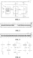
- FIG. 1 is a structural diagram of a magnetoresistive relay 1, including a substrate 2 and a magnetic excitation coil 3, a magnetoresistive sensor 4, and a switch integrated circuit 5 which are placed on the substrate 2, and further including an excitation signal input electrode 6, an output electrode 7, a switch circuit positive output electrode 8, an output electrode 9, a power input electrode 10, and a ground electrode 11.
- the ends of the magnetic excitation coil 3 are each connected with the excitation signal input electrode 6 and the excitation signal output electrode 7.
- the signal from the magnetoresistive sensor 4 is sent to the switch integrated circuit 5.
- the positive switch circuit output electrode 8 and the switch circuit negative electrode 9 are respectively connected with the switch integrated circuit 5.
- the power input ends and the ground ends of the magnetoresistive sensor 4 are respectively connected with the power input electrode 10 and the ground electrode 11.
- the power input ends and the ground ends of the switch integrated circuit 5 are respectively connected with the power input electrode 10 and the ground electrode 11.
- the principle is that, the magnetic field from the excitation coil 3 provides a magnetic excitation field signal Hex, and this signal is used to change the magnetoresistance of the magnetoresistive sensor 4, the switch integrated circuit 5 receives an output signal Vout from the magnetoresistive sensor, and the switch integrated circuit 5 realizes the external output switching action according to the signal of the excitation coil 3.
- FIG. 2 and FIG. 3 are two sectional diagrams of a magnetoresistive relay respectively.
- Structure of the magnetoresistive sensors in FIG. 2 and FIG. 3 include substrates 21 and 31, planar coils 22 and 32 placed on the substrates, magnetoresistive sensors 23 and 33 placed on upper surfaces of the planar coils 22 and 32, and magnetic shielding layers 24 and 34 placed above the magnetoresistive sensors 23 and 33.
- the magnetoresistive sensor is placed between the excitation coil and the magnetic shielding plate. Therefore, another possible sequence may be that a magnetic shielding layer, a magnetoresistive sensor, and an excitation coil are sequentially placed on a substrate.
- the difference between FIG. 2 and FIG. 3 is the difference between structures of the excitation coils 22 and 32.
- the coil 22 is of a spiral structure, and with respect to a central region, coil wires at two sides have opposite current directions, and coil wires at the same side have identical current directions. However, in FIG. 3 , adjacent coil wires have opposite circuit directions.
- FIG. 4 is a structural diagram of a magnetoresistive sensor.
- FIG. 4a shows a reference half-bridge structure
- FIG. 4b shows a push-pull half-bridge structure
- FIG. 4c shows a reference full-bridge structure
- FIG. 4d shows a push-pull full-bridge structure.
- quasi-bridge structures are further included.
- FIG. 5 and FIG. 6 are diagrams showing two typical planar spiral coils and distribution of magnetoresistive sensors on the planar coils.
- 41 and 51 denote magnetic shielding layers
- 42 and 52 both denote spiral coils
- 42 is of a polygon structure
- 52 is of a quadrilateral structure
- 42 includes two section regions 43 and 44
- 52 includes two section regions 53 and 54
- the two regions 43 and 44 and the two regions 53 and 54 each include multiple section of elongated straight wires.
- the elongated straight wires have identical lengths and widths, adjacent elongated straight wires are separated by identical intervals, and elongated straight wires in two regions have opposite current directions.
- the two regions 43 and 44 and the two regions 53 and 54 each have symmetric magnetic field distribution features, that is, magnetic field distribution features perpendicular to the current direction in the two regions are opposite, and this provides conditions for placement of push arms and pull arms of the push-pull magnetoresistive sensor.
- the push-pull magnetoresistive sensor is of a full-bridge structure, and includes 2 push arms and 2 pull arms, thus forming four regions in total.
- the push region 43 includes two sub-regions 45 and 48 for placing push arms
- the pull region 44 includes two sub-regions 46 and 47 for placing pull arms.
- the push region 53 includes two sub-regions 57 and 56 for placing push arms
- the pull region 54 includes two sub-regions 55 and 58 for placing pull arms.
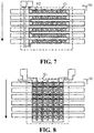
- FIG. 7 and FIG. 8 are diagrams showing arrangements and connections of magnetoresistive sensing units in the push arm region or pull arm region.
- the magnetoresistive sensing units are arranged into an array. All the magnetoresistive sensing units have magnetic sensitive directions perpendicular to the current direction, and form push arm structures or pull arm structures at two ports by parallel connection or serial connection.
- the magnetoresistive sensing units are serially connected to form magnetoresistive sensing unit strings, which are then serially connected to form a two-port structure.
- the magnetoresistive sensing unit strings are parallel to the elongated straight wires, and in FIG.
- the magnetoresistive sensing unit strings are perpendicular to the elongated straight wire. It should be pointed out that the magnetoresistive sensing units are placed directly above or directly below coils in the region. The magnetoresistive sensing units may be placed directly above or directly below centers of the wires, and may also be placed apart from central positions, for example, placed at gaps of the wires. This is because although magnetic fields sensed by the magnetoresistive sensing units are different, magnetic field magnitudes at different places are all proportional to the current intensity of the coil; therefore, the total resistance of the push arm and the pull arm is also proportional to the current intensity.
- the magnetoresistive sensing units in the regions where the push arms and the pull arms are located have completely identical distributions of the elongated straight wire; therefore, the total resistance changes of the push arm and the pull arm are completely identical, and the output of the whole push-pull full-bridge magnetoresistive sensor will be proportional to the amplitude change of the current.
- FIG. 9 and FIG. 10 show distribution features of a twisted planar coil and magnetoresistive sensing unit strings of a magnetoresistive sensor.
- 61 and 71 denote magnetic shielding layers
- 62 and 72 denote twisted planar coils, including multiple elongated straight wires arranged in parallel at equal intervals.
- the elongated straight wires have identical lengths and widths, and adjacent two elongated straight wires are connected in series but have opposite current directions.
- push magnetoresistive sensing unit strings 63 and pull magnetoresistive sensing unit strings 65 are alternately placed directly above or directly below the adjacent two elongated straight wires.
- FIG. 10 corresponds to a magnetoresistive sensor of a reference bridge structure, wherein reference magnetoresistive sensing unit strings 73 and sensitive magnetoresistive sensing unit strings 75 are alternately placed at a central position between two adjacent elongated straight wires, and directly above or directly below the elongated wires adjacent to the central position and both have forward currents or reverse currents.
- FIG. 11 and FIG. 12 are distribution structural diagrams of a three-dimensional coil and magnetoresistive sensing unit strings.
- a structure 200 current directions of a top coil 201 and a bottom coil 202 included in the three-dimensional coil have opposite current directions, as shown in the drawings.
- 203 denotes a reference bridge magnetoresistive sensor.
- a reference arm of the reference bridge magnetoresistive sensor includes a ferromagnetic shielding layer, specifically a soft ferromagnetic flux shielding layer.
- the three-dimensional coil may be a solenoid coil or referred to as a three-dimensional solenoid.
- the three-dimensional solenoid of FIG. 12 includes two solenoids 301 and 302 wound in opposite directions.
- a push magnetoresistive sensing unit 303 and a pull magnetoresistive sensing unit 304 are respectively placed in the solenoids 301 and 302, and since the two have opposite magnetic field directions, a push-pull magnetoresistive sensor bridge is formed.
- FIG. 13 to FIG. 16 respectively show four operation modes of a magnetoresistive relay.
- FIG. 13 shows a single-point operation mode, in which the switch integrated circuit switches from an off state to an on state only when the forward current of the excitation coil is greater than Ion-off, and the switch integrated circuit switches from the on state to the off state only when the forward current of the excitation coil is less than Ion-off
- FIG. 14 shows a bipolar operation mode, in which the switch integrated circuit switches from an off state to an on state only when the forward current of the excitation coil is greater than Ion, and the switch integrated circuit switches from the on state to the off state only when the forward current of the excitation coil is less than Ioff.
- FIG. 15 shows a unipolar operation mode, in which the switch integrated circuit switches from an off state to an on state only when the forward current of the excitation coil is greater than Ion, and the switch integrated circuit switches from the on state to the off state only when the reverse current of the excitation coil is greater than Ioff.
- FIG. 16 shows an omnipolar operation mode, in which the switch integrated circuit switches from an off state to an on state when the forward current of the excitation coil is greater than Ion1, and the switch integrated circuit switches from the on state to the off state when the forward current of the excitation coil is less than Ioff1; or the switch integrated circuit switches from an off state to an on state when the reverse current of the excitation coil is greater than -Ion1, and the switch integrated circuit switches from the on state to the off state when the reverse current of the excitation coil is less than -Ioff1.
- FIG. 17 is a signal processing diagram of a magnetoresistive relay.
- 100 denotes a magnetoresistive sensor, which is a half-bridge magnetoresistive sensor in this embodiment
- 101 denotes a switch integrated circuit
- 102 denotes an external circuit.
- An output signal of the magnetoresistive sensor 100 is denoised after passing through a low-pass filter 103, and then amplified by an amplifier 104. The signal is compared with a reference voltage by a comparator 105, and the signal is output to a latch, control and drive circuit 106.
- an MOSFET tube switch formed by drives 107 and 108 the gates of two MOSFET tubes 107 and 108 are interconnected, a source of 107 and a drain of 108 are interconnected, and the two interconnections are polarly connected to an output end of 106.
- the external circuit 102 is connected to a drain of 107 and a source of 108.
- a magnetic response signal output by the magnetoresistive sensor 100 of the magnetoresistive relay passes the filter 103, the amplifier 104 and the comparator 105, to be transformed into a control, latch, and drive signal of 106, to control the on/off of the switch formed by the two MOSFET tubes 107 and 108, such that switch operation of the external circuit 102 can be realized.
Landscapes
- Physics & Mathematics (AREA)
- Condensed Matter Physics & Semiconductors (AREA)
- General Physics & Mathematics (AREA)
- Measuring Magnetic Variables (AREA)
- Hall/Mr Elements (AREA)
- Electronic Switches (AREA)
Applications Claiming Priority (2)
| Application Number | Priority Date | Filing Date | Title |
|---|---|---|---|
| CN201510493695.6A CN105185655B (zh) | 2015-08-12 | 2015-08-12 | 一种磁电阻继电器 |
| PCT/CN2016/094587 WO2017025044A1 (zh) | 2015-08-12 | 2016-08-11 | 一种磁电阻继电器 |
Publications (3)
| Publication Number | Publication Date |
|---|---|
| EP3336873A1 true EP3336873A1 (de) | 2018-06-20 |
| EP3336873A4 EP3336873A4 (de) | 2019-03-27 |
| EP3336873B1 EP3336873B1 (de) | 2024-07-10 |
Family
ID=54907666
Family Applications (1)
| Application Number | Title | Priority Date | Filing Date |
|---|---|---|---|
| EP16834668.2A Active EP3336873B1 (de) | 2015-08-12 | 2016-08-11 | Magnetoresistives relais |
Country Status (5)
| Country | Link |
|---|---|
| US (1) | US10459042B2 (de) |
| EP (1) | EP3336873B1 (de) |
| JP (1) | JP6827033B2 (de) |
| CN (1) | CN105185655B (de) |
| WO (1) | WO2017025044A1 (de) |
Families Citing this family (13)
| Publication number | Priority date | Publication date | Assignee | Title |
|---|---|---|---|---|
| CN105185655B (zh) * | 2015-08-12 | 2017-08-29 | 江苏多维科技有限公司 | 一种磁电阻继电器 |
| CN107037382B (zh) * | 2017-04-05 | 2023-05-30 | 江苏多维科技有限公司 | 一种预调制磁电阻传感器 |
| CN107064829B (zh) * | 2017-05-04 | 2023-02-21 | 江苏多维科技有限公司 | 一种单芯片高灵敏度磁电阻线性传感器 |
| CN208143202U (zh) * | 2017-12-15 | 2018-11-23 | 江苏多维科技有限公司 | 一种基于磁电阻的双稳态磁开关及系统 |
| DE102018102998A1 (de) | 2018-02-09 | 2019-08-14 | Infineon Technologies Ag | Vorrichtung, Verfahren und Computerprogramm zum Vergleichen der Ausgabe von Sensorzellen |
| CN108987392B (zh) * | 2018-08-14 | 2024-01-02 | 黑龙江大学 | 一种复合磁场传感器及其制作工艺 |
| US11165014B2 (en) * | 2019-03-29 | 2021-11-02 | Ablic Inc. | Semiconductor device |
| CN111277231B (zh) * | 2020-02-18 | 2022-02-18 | 江苏多维科技有限公司 | 一种增益可控的磁阻模拟放大器 |
| CN217406515U (zh) * | 2022-05-12 | 2022-09-09 | 江苏多维科技有限公司 | 一种具有滤波功能的磁开关 |
| US11892524B1 (en) * | 2022-10-13 | 2024-02-06 | Allegro Microsystems, Llc | Reduced area magnetic field sensor topology |
| CN115541984B (zh) * | 2022-11-30 | 2023-03-07 | 中国电力科学研究院有限公司 | 一种自适应微弱电流监测装置及监测方法 |
| CN118054778B (zh) * | 2024-01-08 | 2024-12-06 | 山东航天电子技术研究所 | 一种具备记忆功能的固态开关及控制方法 |
| CN118591262A (zh) * | 2024-04-22 | 2024-09-03 | 淮阴师范学院 | 一种基于独立栅极结构的非互易磁电阻器件及其制备方法 |
Family Cites Families (16)
| Publication number | Priority date | Publication date | Assignee | Title |
|---|---|---|---|---|
| CN2501256Y (zh) * | 2001-10-24 | 2002-07-17 | 库万军 | 磁敏接近开关 |
| JP2009162540A (ja) * | 2007-12-28 | 2009-07-23 | Alps Electric Co Ltd | 磁気センサ及びその製造方法 |
| US8098062B2 (en) * | 2008-08-22 | 2012-01-17 | Honeywell International Inc. | Comparator circuit having latching behavior and digital output sensors therefrom |
| JP2010258979A (ja) * | 2009-04-28 | 2010-11-11 | Alps Green Devices Co Ltd | 磁気結合型アイソレータ |
| JP5523149B2 (ja) * | 2010-03-05 | 2014-06-18 | アルプス電気株式会社 | 磁気式スイッチ |
| US8957676B2 (en) * | 2011-05-06 | 2015-02-17 | Allegro Microsystems, Llc | Magnetic field sensor having a control node to receive a control signal to adjust a threshold |
| CN102790613B (zh) * | 2011-05-16 | 2015-04-29 | 江苏多维科技有限公司 | 一种开关传感器 |
| US9203394B2 (en) * | 2011-10-06 | 2015-12-01 | Infineon Technologies Ag | Integrated magnetic field sensor-controlled switch devices |
| KR101343037B1 (ko) * | 2011-11-10 | 2013-12-18 | 삼성전자 주식회사 | 자기 공명 영상용 무선 고주파 코일, 그 코일의 전원 제어 방법 및 그 코일을 이용한 자기 공명 영상 장치 |
| CN104065367B (zh) | 2013-03-20 | 2017-11-07 | 江苏多维科技有限公司 | 一种低功耗磁电阻开关传感器 |
| WO2014156751A1 (ja) | 2013-03-26 | 2014-10-02 | 株式会社村田製作所 | 磁気センサ |
| CN104104376B (zh) * | 2013-04-01 | 2018-01-02 | 江苏多维科技有限公司 | 推挽式芯片翻转半桥磁阻开关 |
| CN103384141B (zh) * | 2013-07-24 | 2015-05-06 | 江苏多维科技有限公司 | 一种磁阻混频器 |
| CN204129826U (zh) * | 2014-06-23 | 2015-01-28 | 江苏多维科技有限公司 | 一种硬币检测系统 |
| CN105185655B (zh) | 2015-08-12 | 2017-08-29 | 江苏多维科技有限公司 | 一种磁电阻继电器 |
| CN204991599U (zh) * | 2015-08-12 | 2016-01-20 | 江苏多维科技有限公司 | 一种磁电阻继电器 |
-
2015
- 2015-08-12 CN CN201510493695.6A patent/CN105185655B/zh active Active
-
2016
- 2016-08-11 EP EP16834668.2A patent/EP3336873B1/de active Active
- 2016-08-11 WO PCT/CN2016/094587 patent/WO2017025044A1/zh not_active Ceased
- 2016-08-11 JP JP2018506203A patent/JP6827033B2/ja active Active
- 2016-08-11 US US15/749,666 patent/US10459042B2/en active Active
Also Published As
| Publication number | Publication date |
|---|---|
| US20180224509A1 (en) | 2018-08-09 |
| JP6827033B2 (ja) | 2021-02-10 |
| EP3336873A4 (de) | 2019-03-27 |
| CN105185655B (zh) | 2017-08-29 |
| EP3336873B1 (de) | 2024-07-10 |
| WO2017025044A1 (zh) | 2017-02-16 |
| JP2018526900A (ja) | 2018-09-13 |
| US10459042B2 (en) | 2019-10-29 |
| CN105185655A (zh) | 2015-12-23 |
Similar Documents
| Publication | Publication Date | Title |
|---|---|---|
| US10459042B2 (en) | Magnetoresistive relay | |
| CN106662622B (zh) | 一种磁传感器 | |
| JP6812367B2 (ja) | 櫛形y軸磁気抵抗センサ | |
| US10228426B2 (en) | Single chip Z-axis linear magnetoresistive sensor with calibration/initialization coil | |
| JP6189426B2 (ja) | 磁気抵抗歯車センサ | |
| JP7099731B2 (ja) | 多層磁気変調構造を有する低ノイズ磁気抵抗センサ | |
| EP3062119B1 (de) | Magnetsensor mit push-pull-brücke für sehr starke magnetfelder | |
| US8179716B2 (en) | Non-volatile programmable logic gates and adders | |
| CN103645449B (zh) | 一种用于高强度磁场的单芯片参考桥式磁传感器 | |
| EP2983293A1 (de) | Magnetoresistiver push-pull- und flip-chip-halbbrückenschalter | |
| KR20050035251A (ko) | 자기장 센서 및 자기장 센서의 작동 방법 | |
| US20160274196A1 (en) | Magnetic sensor | |
| US20160146859A1 (en) | Current detector | |
| JP2018518677A (ja) | プッシュ−プルx軸磁気抵抗センサ | |
| US20210103015A1 (en) | Resettable bipolar switch sensor | |
| JP2015219227A (ja) | 磁気センサ | |
| EP3373022A1 (de) | Hochempfindlicher einzelchip-tmr-magnetfeldsensor vom push-pull-typ | |
| CN103728573B (zh) | 磁场检测装置和磁场检测方法 | |
| US11181555B2 (en) | Current sensing method and current sensor | |
| CN204991599U (zh) | 一种磁电阻继电器 | |
| EP4451459A1 (de) | Elektrischer abschirmungs-magnettunnelübergangssignalisolator | |
| CN111758040B (zh) | 具有分布的通量引导件的z轴线磁性传感器 | |
| RU156559U1 (ru) | Магниторезистивный преобразователь | |
| JP2008288071A (ja) | 磁気近接スイッチ | |
| RU155241U1 (ru) | Модуль для измерения параметров магнитного поля |
Legal Events
| Date | Code | Title | Description |
|---|---|---|---|
| STAA | Information on the status of an ep patent application or granted ep patent |
Free format text: STATUS: THE INTERNATIONAL PUBLICATION HAS BEEN MADE |
|
| PUAI | Public reference made under article 153(3) epc to a published international application that has entered the european phase |
Free format text: ORIGINAL CODE: 0009012 |
|
| STAA | Information on the status of an ep patent application or granted ep patent |
Free format text: STATUS: REQUEST FOR EXAMINATION WAS MADE |
|
| 17P | Request for examination filed |
Effective date: 20180209 |
|
| AK | Designated contracting states |
Kind code of ref document: A1 Designated state(s): AL AT BE BG CH CY CZ DE DK EE ES FI FR GB GR HR HU IE IS IT LI LT LU LV MC MK MT NL NO PL PT RO RS SE SI SK SM TR |
|
| AX | Request for extension of the european patent |
Extension state: BA ME |
|
| DAV | Request for validation of the european patent (deleted) | ||
| DAX | Request for extension of the european patent (deleted) | ||
| A4 | Supplementary search report drawn up and despatched |
Effective date: 20190226 |
|
| RIC1 | Information provided on ipc code assigned before grant |
Ipc: H03K 17/689 20060101ALI20190220BHEP Ipc: H01H 47/02 20060101AFI20190220BHEP |
|
| STAA | Information on the status of an ep patent application or granted ep patent |
Free format text: STATUS: EXAMINATION IS IN PROGRESS |
|
| 17Q | First examination report despatched |
Effective date: 20200318 |
|
| RAP3 | Party data changed (applicant data changed or rights of an application transferred) |
Owner name: MULTIDIMENSION TECHNOLOGY CO., LTD. |
|
| RAP3 | Party data changed (applicant data changed or rights of an application transferred) |
Owner name: MULTIDIMENSION TECHNOLOGY CO., LTD. |
|
| RIN1 | Information on inventor provided before grant (corrected) |
Inventor name: DEAK, JAMES GEZA Inventor name: ZHOU, ZHIMIN |
|
| RAP3 | Party data changed (applicant data changed or rights of an application transferred) |
Owner name: MULTIDIMENSION TECHNOLOGY CO., LTD. |
|
| RAP3 | Party data changed (applicant data changed or rights of an application transferred) |
Owner name: MULTIDIMENSION TECHNOLOGY CO., LTD. |
|
| RIN1 | Information on inventor provided before grant (corrected) |
Inventor name: DEAK, JAMES GEZA Inventor name: ZHOU, ZHIMIN |
|
| REG | Reference to a national code |
Ref legal event code: R079 Ipc: H03K0017689000 Ref country code: DE Ref document number: 602016088368 Country of ref document: DE Free format text: PREVIOUS MAIN CLASS: H01H0047020000 |
|
| P01 | Opt-out of the competence of the unified patent court (upc) registered |
Effective date: 20230626 |
|
| RIC1 | Information provided on ipc code assigned before grant |
Ipc: H03K 17/90 20060101ALI20230727BHEP Ipc: H01H 47/02 20060101ALI20230727BHEP Ipc: H03K 17/689 20060101AFI20230727BHEP |
|
| GRAP | Despatch of communication of intention to grant a patent |
Free format text: ORIGINAL CODE: EPIDOSNIGR1 |
|
| STAA | Information on the status of an ep patent application or granted ep patent |
Free format text: STATUS: GRANT OF PATENT IS INTENDED |
|
| INTG | Intention to grant announced |
Effective date: 20230911 |
|
| GRAJ | Information related to disapproval of communication of intention to grant by the applicant or resumption of examination proceedings by the epo deleted |
Free format text: ORIGINAL CODE: EPIDOSDIGR1 |
|
| STAA | Information on the status of an ep patent application or granted ep patent |
Free format text: STATUS: EXAMINATION IS IN PROGRESS |
|
| INTC | Intention to grant announced (deleted) | ||
| GRAP | Despatch of communication of intention to grant a patent |
Free format text: ORIGINAL CODE: EPIDOSNIGR1 |
|
| STAA | Information on the status of an ep patent application or granted ep patent |
Free format text: STATUS: GRANT OF PATENT IS INTENDED |
|
| INTG | Intention to grant announced |
Effective date: 20240226 |
|
| GRAS | Grant fee paid |
Free format text: ORIGINAL CODE: EPIDOSNIGR3 |
|
| GRAA | (expected) grant |
Free format text: ORIGINAL CODE: 0009210 |
|
| STAA | Information on the status of an ep patent application or granted ep patent |
Free format text: STATUS: THE PATENT HAS BEEN GRANTED |
|
| AK | Designated contracting states |
Kind code of ref document: B1 Designated state(s): AL AT BE BG CH CY CZ DE DK EE ES FI FR GB GR HR HU IE IS IT LI LT LU LV MC MK MT NL NO PL PT RO RS SE SI SK SM TR |
|
| REG | Reference to a national code |
Ref country code: CH Ref legal event code: EP |
|
| REG | Reference to a national code |
Ref country code: DE Ref legal event code: R096 Ref document number: 602016088368 Country of ref document: DE |
|
| REG | Reference to a national code |
Ref country code: LT Ref legal event code: MG9D |
|
| REG | Reference to a national code |
Ref country code: NL Ref legal event code: MP Effective date: 20240710 |
|
| PG25 | Lapsed in a contracting state [announced via postgrant information from national office to epo] |
Ref country code: PT Free format text: LAPSE BECAUSE OF FAILURE TO SUBMIT A TRANSLATION OF THE DESCRIPTION OR TO PAY THE FEE WITHIN THE PRESCRIBED TIME-LIMIT Effective date: 20241111 |
|
| REG | Reference to a national code |
Ref country code: AT Ref legal event code: MK05 Ref document number: 1702938 Country of ref document: AT Kind code of ref document: T Effective date: 20240710 |
|
| PG25 | Lapsed in a contracting state [announced via postgrant information from national office to epo] |
Ref country code: NL Free format text: LAPSE BECAUSE OF FAILURE TO SUBMIT A TRANSLATION OF THE DESCRIPTION OR TO PAY THE FEE WITHIN THE PRESCRIBED TIME-LIMIT Effective date: 20240710 |
|
| PG25 | Lapsed in a contracting state [announced via postgrant information from national office to epo] |
Ref country code: PT Free format text: LAPSE BECAUSE OF FAILURE TO SUBMIT A TRANSLATION OF THE DESCRIPTION OR TO PAY THE FEE WITHIN THE PRESCRIBED TIME-LIMIT Effective date: 20241111 Ref country code: NL Free format text: LAPSE BECAUSE OF FAILURE TO SUBMIT A TRANSLATION OF THE DESCRIPTION OR TO PAY THE FEE WITHIN THE PRESCRIBED TIME-LIMIT Effective date: 20240710 |
|
| PG25 | Lapsed in a contracting state [announced via postgrant information from national office to epo] |
Ref country code: NO Free format text: LAPSE BECAUSE OF FAILURE TO SUBMIT A TRANSLATION OF THE DESCRIPTION OR TO PAY THE FEE WITHIN THE PRESCRIBED TIME-LIMIT Effective date: 20241010 |
|
| PG25 | Lapsed in a contracting state [announced via postgrant information from national office to epo] |
Ref country code: GR Free format text: LAPSE BECAUSE OF FAILURE TO SUBMIT A TRANSLATION OF THE DESCRIPTION OR TO PAY THE FEE WITHIN THE PRESCRIBED TIME-LIMIT Effective date: 20241011 Ref country code: PL Free format text: LAPSE BECAUSE OF FAILURE TO SUBMIT A TRANSLATION OF THE DESCRIPTION OR TO PAY THE FEE WITHIN THE PRESCRIBED TIME-LIMIT Effective date: 20240710 Ref country code: FI Free format text: LAPSE BECAUSE OF FAILURE TO SUBMIT A TRANSLATION OF THE DESCRIPTION OR TO PAY THE FEE WITHIN THE PRESCRIBED TIME-LIMIT Effective date: 20240710 |
|
| PG25 | Lapsed in a contracting state [announced via postgrant information from national office to epo] |
Ref country code: BG Free format text: LAPSE BECAUSE OF FAILURE TO SUBMIT A TRANSLATION OF THE DESCRIPTION OR TO PAY THE FEE WITHIN THE PRESCRIBED TIME-LIMIT Effective date: 20240710 |
|
| PG25 | Lapsed in a contracting state [announced via postgrant information from national office to epo] |
Ref country code: LV Free format text: LAPSE BECAUSE OF FAILURE TO SUBMIT A TRANSLATION OF THE DESCRIPTION OR TO PAY THE FEE WITHIN THE PRESCRIBED TIME-LIMIT Effective date: 20240710 |
|
| PG25 | Lapsed in a contracting state [announced via postgrant information from national office to epo] |
Ref country code: IS Free format text: LAPSE BECAUSE OF FAILURE TO SUBMIT A TRANSLATION OF THE DESCRIPTION OR TO PAY THE FEE WITHIN THE PRESCRIBED TIME-LIMIT Effective date: 20241110 Ref country code: AT Free format text: LAPSE BECAUSE OF FAILURE TO SUBMIT A TRANSLATION OF THE DESCRIPTION OR TO PAY THE FEE WITHIN THE PRESCRIBED TIME-LIMIT Effective date: 20240710 |
|
| PG25 | Lapsed in a contracting state [announced via postgrant information from national office to epo] |
Ref country code: HR Free format text: LAPSE BECAUSE OF FAILURE TO SUBMIT A TRANSLATION OF THE DESCRIPTION OR TO PAY THE FEE WITHIN THE PRESCRIBED TIME-LIMIT Effective date: 20240710 |
|
| PG25 | Lapsed in a contracting state [announced via postgrant information from national office to epo] |
Ref country code: RS Free format text: LAPSE BECAUSE OF FAILURE TO SUBMIT A TRANSLATION OF THE DESCRIPTION OR TO PAY THE FEE WITHIN THE PRESCRIBED TIME-LIMIT Effective date: 20241010 Ref country code: ES Free format text: LAPSE BECAUSE OF FAILURE TO SUBMIT A TRANSLATION OF THE DESCRIPTION OR TO PAY THE FEE WITHIN THE PRESCRIBED TIME-LIMIT Effective date: 20240710 |
|
| PG25 | Lapsed in a contracting state [announced via postgrant information from national office to epo] |
Ref country code: RS Free format text: LAPSE BECAUSE OF FAILURE TO SUBMIT A TRANSLATION OF THE DESCRIPTION OR TO PAY THE FEE WITHIN THE PRESCRIBED TIME-LIMIT Effective date: 20241010 Ref country code: PL Free format text: LAPSE BECAUSE OF FAILURE TO SUBMIT A TRANSLATION OF THE DESCRIPTION OR TO PAY THE FEE WITHIN THE PRESCRIBED TIME-LIMIT Effective date: 20240710 Ref country code: NO Free format text: LAPSE BECAUSE OF FAILURE TO SUBMIT A TRANSLATION OF THE DESCRIPTION OR TO PAY THE FEE WITHIN THE PRESCRIBED TIME-LIMIT Effective date: 20241010 Ref country code: LV Free format text: LAPSE BECAUSE OF FAILURE TO SUBMIT A TRANSLATION OF THE DESCRIPTION OR TO PAY THE FEE WITHIN THE PRESCRIBED TIME-LIMIT Effective date: 20240710 Ref country code: IS Free format text: LAPSE BECAUSE OF FAILURE TO SUBMIT A TRANSLATION OF THE DESCRIPTION OR TO PAY THE FEE WITHIN THE PRESCRIBED TIME-LIMIT Effective date: 20241110 Ref country code: HR Free format text: LAPSE BECAUSE OF FAILURE TO SUBMIT A TRANSLATION OF THE DESCRIPTION OR TO PAY THE FEE WITHIN THE PRESCRIBED TIME-LIMIT Effective date: 20240710 Ref country code: GR Free format text: LAPSE BECAUSE OF FAILURE TO SUBMIT A TRANSLATION OF THE DESCRIPTION OR TO PAY THE FEE WITHIN THE PRESCRIBED TIME-LIMIT Effective date: 20241011 Ref country code: FI Free format text: LAPSE BECAUSE OF FAILURE TO SUBMIT A TRANSLATION OF THE DESCRIPTION OR TO PAY THE FEE WITHIN THE PRESCRIBED TIME-LIMIT Effective date: 20240710 Ref country code: ES Free format text: LAPSE BECAUSE OF FAILURE TO SUBMIT A TRANSLATION OF THE DESCRIPTION OR TO PAY THE FEE WITHIN THE PRESCRIBED TIME-LIMIT Effective date: 20240710 Ref country code: BG Free format text: LAPSE BECAUSE OF FAILURE TO SUBMIT A TRANSLATION OF THE DESCRIPTION OR TO PAY THE FEE WITHIN THE PRESCRIBED TIME-LIMIT Effective date: 20240710 Ref country code: AT Free format text: LAPSE BECAUSE OF FAILURE TO SUBMIT A TRANSLATION OF THE DESCRIPTION OR TO PAY THE FEE WITHIN THE PRESCRIBED TIME-LIMIT Effective date: 20240710 |
|
| REG | Reference to a national code |
Ref country code: CH Ref legal event code: PL |
|
| REG | Reference to a national code |
Ref country code: DE Ref legal event code: R097 Ref document number: 602016088368 Country of ref document: DE |
|
| PG25 | Lapsed in a contracting state [announced via postgrant information from national office to epo] |
Ref country code: DK Free format text: LAPSE BECAUSE OF FAILURE TO SUBMIT A TRANSLATION OF THE DESCRIPTION OR TO PAY THE FEE WITHIN THE PRESCRIBED TIME-LIMIT Effective date: 20240710 Ref country code: SM Free format text: LAPSE BECAUSE OF FAILURE TO SUBMIT A TRANSLATION OF THE DESCRIPTION OR TO PAY THE FEE WITHIN THE PRESCRIBED TIME-LIMIT Effective date: 20240710 Ref country code: RO Free format text: LAPSE BECAUSE OF FAILURE TO SUBMIT A TRANSLATION OF THE DESCRIPTION OR TO PAY THE FEE WITHIN THE PRESCRIBED TIME-LIMIT Effective date: 20240710 |
|
| PG25 | Lapsed in a contracting state [announced via postgrant information from national office to epo] |
Ref country code: LU Free format text: LAPSE BECAUSE OF NON-PAYMENT OF DUE FEES Effective date: 20240811 |
|
| PG25 | Lapsed in a contracting state [announced via postgrant information from national office to epo] |
Ref country code: EE Free format text: LAPSE BECAUSE OF FAILURE TO SUBMIT A TRANSLATION OF THE DESCRIPTION OR TO PAY THE FEE WITHIN THE PRESCRIBED TIME-LIMIT Effective date: 20240710 Ref country code: MC Free format text: LAPSE BECAUSE OF FAILURE TO SUBMIT A TRANSLATION OF THE DESCRIPTION OR TO PAY THE FEE WITHIN THE PRESCRIBED TIME-LIMIT Effective date: 20240710 Ref country code: CH Free format text: LAPSE BECAUSE OF NON-PAYMENT OF DUE FEES Effective date: 20240831 |
|
| PG25 | Lapsed in a contracting state [announced via postgrant information from national office to epo] |
Ref country code: CZ Free format text: LAPSE BECAUSE OF FAILURE TO SUBMIT A TRANSLATION OF THE DESCRIPTION OR TO PAY THE FEE WITHIN THE PRESCRIBED TIME-LIMIT Effective date: 20240710 |
|
| PG25 | Lapsed in a contracting state [announced via postgrant information from national office to epo] |
Ref country code: SK Free format text: LAPSE BECAUSE OF FAILURE TO SUBMIT A TRANSLATION OF THE DESCRIPTION OR TO PAY THE FEE WITHIN THE PRESCRIBED TIME-LIMIT Effective date: 20240710 Ref country code: IT Free format text: LAPSE BECAUSE OF FAILURE TO SUBMIT A TRANSLATION OF THE DESCRIPTION OR TO PAY THE FEE WITHIN THE PRESCRIBED TIME-LIMIT Effective date: 20240710 |
|
| PLBE | No opposition filed within time limit |
Free format text: ORIGINAL CODE: 0009261 |
|
| STAA | Information on the status of an ep patent application or granted ep patent |
Free format text: STATUS: NO OPPOSITION FILED WITHIN TIME LIMIT |
|
| 26N | No opposition filed |
Effective date: 20250411 |
|
| REG | Reference to a national code |
Ref country code: BE Ref legal event code: MM Effective date: 20240831 |
|
| PG25 | Lapsed in a contracting state [announced via postgrant information from national office to epo] |
Ref country code: BE Free format text: LAPSE BECAUSE OF NON-PAYMENT OF DUE FEES Effective date: 20240831 |
|
| PG25 | Lapsed in a contracting state [announced via postgrant information from national office to epo] |
Ref country code: IE Free format text: LAPSE BECAUSE OF NON-PAYMENT OF DUE FEES Effective date: 20240811 |
|
| PG25 | Lapsed in a contracting state [announced via postgrant information from national office to epo] |
Ref country code: SE Free format text: LAPSE BECAUSE OF FAILURE TO SUBMIT A TRANSLATION OF THE DESCRIPTION OR TO PAY THE FEE WITHIN THE PRESCRIBED TIME-LIMIT Effective date: 20240710 |
|
| PGFP | Annual fee paid to national office [announced via postgrant information from national office to epo] |
Ref country code: DE Payment date: 20250827 Year of fee payment: 10 |
|
| PGFP | Annual fee paid to national office [announced via postgrant information from national office to epo] |
Ref country code: GB Payment date: 20250827 Year of fee payment: 10 |
|
| PGFP | Annual fee paid to national office [announced via postgrant information from national office to epo] |
Ref country code: FR Payment date: 20250825 Year of fee payment: 10 |
|
| PG25 | Lapsed in a contracting state [announced via postgrant information from national office to epo] |
Ref country code: CY Free format text: LAPSE BECAUSE OF FAILURE TO SUBMIT A TRANSLATION OF THE DESCRIPTION OR TO PAY THE FEE WITHIN THE PRESCRIBED TIME-LIMIT; INVALID AB INITIO Effective date: 20160811 |
|
| PG25 | Lapsed in a contracting state [announced via postgrant information from national office to epo] |
Ref country code: HU Free format text: LAPSE BECAUSE OF FAILURE TO SUBMIT A TRANSLATION OF THE DESCRIPTION OR TO PAY THE FEE WITHIN THE PRESCRIBED TIME-LIMIT; INVALID AB INITIO Effective date: 20160811 |