EP3336879A1 - Verfahren zur herstellung eines siliciumcarbidhalbleiterbauelements sowie siliciumcarbidhalbleiterbauelement - Google Patents
Verfahren zur herstellung eines siliciumcarbidhalbleiterbauelements sowie siliciumcarbidhalbleiterbauelement Download PDFInfo
- Publication number
- EP3336879A1 EP3336879A1 EP15889428.7A EP15889428A EP3336879A1 EP 3336879 A1 EP3336879 A1 EP 3336879A1 EP 15889428 A EP15889428 A EP 15889428A EP 3336879 A1 EP3336879 A1 EP 3336879A1
- Authority
- EP
- European Patent Office
- Prior art keywords
- silicon carbide
- carbide semiconductor
- semiconductor device
- base body
- manufacturing
- Prior art date
- Legal status (The legal status is an assumption and is not a legal conclusion. Google has not performed a legal analysis and makes no representation as to the accuracy of the status listed.)
- Granted
Links
Images


Classifications
-
- H—ELECTRICITY
- H10—SEMICONDUCTOR DEVICES; ELECTRIC SOLID-STATE DEVICES NOT OTHERWISE PROVIDED FOR
- H10P—GENERIC PROCESSES OR APPARATUS FOR THE MANUFACTURE OR TREATMENT OF DEVICES COVERED BY CLASS H10
- H10P14/00—Formation of materials, e.g. in the shape of layers or pillars
- H10P14/20—Formation of materials, e.g. in the shape of layers or pillars of semiconductor materials
- H10P14/34—Deposited materials, e.g. layers
- H10P14/3402—Deposited materials, e.g. layers characterised by the chemical composition
- H10P14/3404—Deposited materials, e.g. layers characterised by the chemical composition being Group IVA materials
- H10P14/3408—Silicon carbide
-
- H—ELECTRICITY
- H10—SEMICONDUCTOR DEVICES; ELECTRIC SOLID-STATE DEVICES NOT OTHERWISE PROVIDED FOR
- H10D—INORGANIC ELECTRIC SEMICONDUCTOR DEVICES
- H10D12/00—Bipolar devices controlled by the field effect, e.g. insulated-gate bipolar transistors [IGBT]
- H10D12/01—Manufacture or treatment
- H10D12/031—Manufacture or treatment of IGBTs
-
- H—ELECTRICITY
- H10—SEMICONDUCTOR DEVICES; ELECTRIC SOLID-STATE DEVICES NOT OTHERWISE PROVIDED FOR
- H10D—INORGANIC ELECTRIC SEMICONDUCTOR DEVICES
- H10D12/00—Bipolar devices controlled by the field effect, e.g. insulated-gate bipolar transistors [IGBT]
- H10D12/01—Manufacture or treatment
- H10D12/031—Manufacture or treatment of IGBTs
- H10D12/032—Manufacture or treatment of IGBTs of vertical IGBTs
-
- H—ELECTRICITY
- H10—SEMICONDUCTOR DEVICES; ELECTRIC SOLID-STATE DEVICES NOT OTHERWISE PROVIDED FOR
- H10D—INORGANIC ELECTRIC SEMICONDUCTOR DEVICES
- H10D30/00—Field-effect transistors [FET]
- H10D30/01—Manufacture or treatment
- H10D30/021—Manufacture or treatment of FETs having insulated gates [IGFET]
- H10D30/028—Manufacture or treatment of FETs having insulated gates [IGFET] of double-diffused metal oxide semiconductor [DMOS] FETs
- H10D30/0291—Manufacture or treatment of FETs having insulated gates [IGFET] of double-diffused metal oxide semiconductor [DMOS] FETs of vertical DMOS [VDMOS] FETs
-
- H—ELECTRICITY
- H10—SEMICONDUCTOR DEVICES; ELECTRIC SOLID-STATE DEVICES NOT OTHERWISE PROVIDED FOR
- H10D—INORGANIC ELECTRIC SEMICONDUCTOR DEVICES
- H10D62/00—Semiconductor bodies, or regions thereof, of devices having potential barriers
- H10D62/10—Shapes, relative sizes or dispositions of the regions of the semiconductor bodies; Shapes of the semiconductor bodies
- H10D62/117—Shapes of semiconductor bodies
-
- H—ELECTRICITY
- H10—SEMICONDUCTOR DEVICES; ELECTRIC SOLID-STATE DEVICES NOT OTHERWISE PROVIDED FOR
- H10D—INORGANIC ELECTRIC SEMICONDUCTOR DEVICES
- H10D62/00—Semiconductor bodies, or regions thereof, of devices having potential barriers
- H10D62/50—Physical imperfections
- H10D62/57—Physical imperfections the imperfections being on the surface of the semiconductor body, e.g. the body having a roughened surface
-
- H—ELECTRICITY
- H10—SEMICONDUCTOR DEVICES; ELECTRIC SOLID-STATE DEVICES NOT OTHERWISE PROVIDED FOR
- H10D—INORGANIC ELECTRIC SEMICONDUCTOR DEVICES
- H10D62/00—Semiconductor bodies, or regions thereof, of devices having potential barriers
- H10D62/80—Semiconductor bodies, or regions thereof, of devices having potential barriers characterised by the materials
- H10D62/83—Semiconductor bodies, or regions thereof, of devices having potential barriers characterised by the materials being Group IV materials, e.g. B-doped Si or undoped Ge
- H10D62/832—Semiconductor bodies, or regions thereof, of devices having potential barriers characterised by the materials being Group IV materials, e.g. B-doped Si or undoped Ge being Group IV materials comprising two or more elements, e.g. SiGe
- H10D62/8325—Silicon carbide
-
- H—ELECTRICITY
- H10—SEMICONDUCTOR DEVICES; ELECTRIC SOLID-STATE DEVICES NOT OTHERWISE PROVIDED FOR
- H10D—INORGANIC ELECTRIC SEMICONDUCTOR DEVICES
- H10D64/00—Electrodes of devices having potential barriers
- H10D64/01—Manufacture or treatment
- H10D64/011—Manufacture or treatment of electrodes ohmically coupled to a semiconductor
-
- H—ELECTRICITY
- H10—SEMICONDUCTOR DEVICES; ELECTRIC SOLID-STATE DEVICES NOT OTHERWISE PROVIDED FOR
- H10D—INORGANIC ELECTRIC SEMICONDUCTOR DEVICES
- H10D64/00—Electrodes of devices having potential barriers
- H10D64/01—Manufacture or treatment
- H10D64/011—Manufacture or treatment of electrodes ohmically coupled to a semiconductor
- H10D64/0111—Manufacture or treatment of electrodes ohmically coupled to a semiconductor to Group IV semiconductors
- H10D64/0115—Manufacture or treatment of electrodes ohmically coupled to a semiconductor to Group IV semiconductors to silicon carbide
-
- H—ELECTRICITY
- H10—SEMICONDUCTOR DEVICES; ELECTRIC SOLID-STATE DEVICES NOT OTHERWISE PROVIDED FOR
- H10D—INORGANIC ELECTRIC SEMICONDUCTOR DEVICES
- H10D64/00—Electrodes of devices having potential barriers
- H10D64/60—Electrodes characterised by their materials
- H10D64/62—Electrodes ohmically coupled to a semiconductor
-
- H—ELECTRICITY
- H10—SEMICONDUCTOR DEVICES; ELECTRIC SOLID-STATE DEVICES NOT OTHERWISE PROVIDED FOR
- H10D—INORGANIC ELECTRIC SEMICONDUCTOR DEVICES
- H10D8/00—Diodes
- H10D8/01—Manufacture or treatment
- H10D8/043—Manufacture or treatment of planar diodes
-
- H—ELECTRICITY
- H10—SEMICONDUCTOR DEVICES; ELECTRIC SOLID-STATE DEVICES NOT OTHERWISE PROVIDED FOR
- H10D—INORGANIC ELECTRIC SEMICONDUCTOR DEVICES
- H10D8/00—Diodes
- H10D8/01—Manufacture or treatment
- H10D8/051—Manufacture or treatment of Schottky diodes
-
- H—ELECTRICITY
- H10—SEMICONDUCTOR DEVICES; ELECTRIC SOLID-STATE DEVICES NOT OTHERWISE PROVIDED FOR
- H10D—INORGANIC ELECTRIC SEMICONDUCTOR DEVICES
- H10D8/00—Diodes
- H10D8/411—PN diodes having planar bodies
-
- H—ELECTRICITY
- H10—SEMICONDUCTOR DEVICES; ELECTRIC SOLID-STATE DEVICES NOT OTHERWISE PROVIDED FOR
- H10D—INORGANIC ELECTRIC SEMICONDUCTOR DEVICES
- H10D8/00—Diodes
- H10D8/50—PIN diodes
-
- H—ELECTRICITY
- H10—SEMICONDUCTOR DEVICES; ELECTRIC SOLID-STATE DEVICES NOT OTHERWISE PROVIDED FOR
- H10D—INORGANIC ELECTRIC SEMICONDUCTOR DEVICES
- H10D8/00—Diodes
- H10D8/60—Schottky-barrier diodes
-
- H—ELECTRICITY
- H10—SEMICONDUCTOR DEVICES; ELECTRIC SOLID-STATE DEVICES NOT OTHERWISE PROVIDED FOR
- H10P—GENERIC PROCESSES OR APPARATUS FOR THE MANUFACTURE OR TREATMENT OF DEVICES COVERED BY CLASS H10
- H10P14/00—Formation of materials, e.g. in the shape of layers or pillars
- H10P14/60—Formation of materials, e.g. in the shape of layers or pillars of insulating materials
- H10P14/69—Inorganic materials
- H10P14/692—Inorganic materials composed of oxides, glassy oxides or oxide-based glasses
- H10P14/6938—Inorganic materials composed of oxides, glassy oxides or oxide-based glasses the material containing at least one metal element, e.g. metal oxides, metal oxynitrides or metal oxycarbides
- H10P14/6939—Inorganic materials composed of oxides, glassy oxides or oxide-based glasses the material containing at least one metal element, e.g. metal oxides, metal oxynitrides or metal oxycarbides characterised by the metal
- H10P14/69393—Inorganic materials composed of oxides, glassy oxides or oxide-based glasses the material containing at least one metal element, e.g. metal oxides, metal oxynitrides or metal oxycarbides characterised by the metal the material containing tantalum, e.g. Ta2O5
-
- H—ELECTRICITY
- H10—SEMICONDUCTOR DEVICES; ELECTRIC SOLID-STATE DEVICES NOT OTHERWISE PROVIDED FOR
- H10P—GENERIC PROCESSES OR APPARATUS FOR THE MANUFACTURE OR TREATMENT OF DEVICES COVERED BY CLASS H10
- H10P14/00—Formation of materials, e.g. in the shape of layers or pillars
- H10P14/60—Formation of materials, e.g. in the shape of layers or pillars of insulating materials
- H10P14/69—Inorganic materials
- H10P14/692—Inorganic materials composed of oxides, glassy oxides or oxide-based glasses
- H10P14/6938—Inorganic materials composed of oxides, glassy oxides or oxide-based glasses the material containing at least one metal element, e.g. metal oxides, metal oxynitrides or metal oxycarbides
- H10P14/6939—Inorganic materials composed of oxides, glassy oxides or oxide-based glasses the material containing at least one metal element, e.g. metal oxides, metal oxynitrides or metal oxycarbides characterised by the metal
- H10P14/69394—Inorganic materials composed of oxides, glassy oxides or oxide-based glasses the material containing at least one metal element, e.g. metal oxides, metal oxynitrides or metal oxycarbides characterised by the metal the material containing titanium, e.g. TiO2
-
- H—ELECTRICITY
- H10—SEMICONDUCTOR DEVICES; ELECTRIC SOLID-STATE DEVICES NOT OTHERWISE PROVIDED FOR
- H10P—GENERIC PROCESSES OR APPARATUS FOR THE MANUFACTURE OR TREATMENT OF DEVICES COVERED BY CLASS H10
- H10P50/00—Etching of wafers, substrates or parts of devices
-
- H—ELECTRICITY
- H10—SEMICONDUCTOR DEVICES; ELECTRIC SOLID-STATE DEVICES NOT OTHERWISE PROVIDED FOR
- H10D—INORGANIC ELECTRIC SEMICONDUCTOR DEVICES
- H10D30/00—Field-effect transistors [FET]
- H10D30/60—Insulated-gate field-effect transistors [IGFET]
- H10D30/64—Double-diffused metal-oxide semiconductor [DMOS] FETs
- H10D30/66—Vertical DMOS [VDMOS] FETs
-
- H—ELECTRICITY
- H10—SEMICONDUCTOR DEVICES; ELECTRIC SOLID-STATE DEVICES NOT OTHERWISE PROVIDED FOR
- H10D—INORGANIC ELECTRIC SEMICONDUCTOR DEVICES
- H10D62/00—Semiconductor bodies, or regions thereof, of devices having potential barriers
- H10D62/10—Shapes, relative sizes or dispositions of the regions of the semiconductor bodies; Shapes of the semiconductor bodies
- H10D62/102—Constructional design considerations for preventing surface leakage or controlling electric field concentration
- H10D62/103—Constructional design considerations for preventing surface leakage or controlling electric field concentration for increasing or controlling the breakdown voltage of reverse-biased devices
- H10D62/105—Constructional design considerations for preventing surface leakage or controlling electric field concentration for increasing or controlling the breakdown voltage of reverse-biased devices by having particular doping profiles, shapes or arrangements of PN junctions; by having supplementary regions, e.g. junction termination extension [JTE]
-
- H—ELECTRICITY
- H10—SEMICONDUCTOR DEVICES; ELECTRIC SOLID-STATE DEVICES NOT OTHERWISE PROVIDED FOR
- H10P—GENERIC PROCESSES OR APPARATUS FOR THE MANUFACTURE OR TREATMENT OF DEVICES COVERED BY CLASS H10
- H10P34/00—Irradiation with electromagnetic or particle radiation of wafers, substrates or parts of devices
- H10P34/40—Irradiation with electromagnetic or particle radiation of wafers, substrates or parts of devices with high-energy radiation
- H10P34/42—Irradiation with electromagnetic or particle radiation of wafers, substrates or parts of devices with high-energy radiation with electromagnetic radiation, e.g. laser annealing
Definitions
- the present invention relates to a method of manufacturing a silicon carbide semiconductor device and a silicon carbide semiconductor device.
- an Ni silicide layer is formed on a silicon carbide semiconductor base body by a silicide process where an Ni thin film is formed on a silicon carbide semiconductor base body and, thereafter, heat treatment is performed.
- heat treatment at a temperature of 1000°C or above is necessary. Accordingly, when an element is formed on the silicon carbide semiconductor base body in advance, there exists a drawback that the element is broken.
- a second method which can overcome the above-mentioned drawback has been known (see patent literature 1, for example).
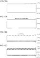
- the second method is performed as follows. An element (MOS structure) not shown in the drawing is formed on a first main surface 912 of a silicon carbide semiconductor base body 910 (see Fig. 10A and Fig. 10B ). Then, a protective film 916 is formed on the first main surface 912 of the silicon carbide semiconductor base body 910 and, thereafter, unevenness is formed on a second main surface 914 of the silicon carbide semiconductor base body 910 by polishing the second main surface 914 (see Fig. 10C ).
- a thin metal film 918 made of metal capable of forming silicide (for example, an Ni thin film) is formed on the second main surface 914 (see Fig. 10D ).
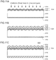
- a metal silicide layer 920 is formed between the silicon carbide semiconductor base body 910 and the thin metal film 918 by irradiating a laser beam which falls within an ultraviolet region onto the thin metal film 918 thus forming an ohmic electrode 924 (see Fig. 11A ).
- a drain electrode 926 is formed on the ohmic electrode 924 (see Fig. 11B ), and a source electrode 928 and a gate electrode not shown in the drawing are formed on a first main surface 912 side of the silicon carbide semiconductor base body 910 (see Fig. 11C ) thus manufacturing a power MOSFET.
- the metal silicide layer is formed by irradiating a laser beam which falls within an ultraviolet region and hence, unlike the above-mentioned first method, heat treatment at a high temperature becomes unnecessary. Accordingly, even when an element is formed on a silicon carbide semiconductor base body in advance, there is no possibility that the element is broken whereby an ohmic electrode can be formed after the element is formed on the silicon carbide semiconductor base body.
- Patent Literature 1 Japanese Patent No. 5460975
- the present invention has been made to overcome the above-mentioned drawback, and it is an object of the present invention to provide a method of manufacturing a silicon carbide semiconductor device and a silicon carbide semiconductor device where an ohmic electrode having an excellent resistance characteristic and an excellent adhesive characteristic can be manufactured at a low manufacturing cost without giving rise to a problem on carbon precipitation.
- a metal carbide is formed by irradiating a laser beam which falls within a visible region or within an infrared region to a thin metal film made of metal capable of forming a metal carbide so that an ohmic electrode can be formed and hence, there arises no problem of carbon precipitation.
- an attenuation coefficient of the thin metal film is higher in a visible region than in an ultraviolet region and hence, a metal carbonization reaction can be sufficiently accelerated whereby a resistance characteristic and an adhesive characteristic of an ohmic electrode are minimally deteriorated.
- a device which irradiates a laser beam which falls within a visible region or within an infrared region is less costly than a device which irradiates a laser beam which falls within an ultraviolet region and hence, a manufacturing cost becomes low compared to a conventional method of manufacturing a silicon carbide semiconductor device.
- the method of manufacturing a silicon carbide semiconductor device of the present invention is a method of manufacturing a silicon carbide semiconductor device capable of manufacturing an ohmic electrode having an excellent resistance characteristic and an excellent adhesive characteristic at a low manufacturing cost without causing a problem of carbon precipitation.
- the silicon carbide semiconductor device according to the present invention can be manufactured by the above-mentioned method of manufacturing a silicon carbide semiconductor device and hence, it is possible to provide an inexpensive silicon carbide semiconductor device which includes an ohmic electrode having an excellent resistance characteristic and an excellent adhesive characteristic without causing a problem of carbon precipitation.
- An embodiment 1 is an embodiment relating to a pn diode.
- a method of manufacturing a silicon carbide semiconductor device according to the embodiment 1 includes, in the following order: a silicon carbide semiconductor base body preparation step; a polishing step; a thin metal film forming step; a laser beam irradiating step; an etching step; and an electrode layer forming step.
- a silicon carbide semiconductor base body preparation step includes, in the following order: a silicon carbide semiconductor base body preparation step; a polishing step; a thin metal film forming step; a laser beam irradiating step; an etching step; and an electrode layer forming step.
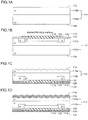
- the method of manufacturing a silicon carbide semiconductor device according to the embodiment 1 is described in detail with reference to Fig. 1A to Fig. 3 .
- the silicon carbide semiconductor base body preparation step is a step of preparing a silicon carbide semiconductor base body 110 which has a first main surface 112 forming an element forming surface and a second main surface 114 forming a surface opposite to the first main surface 112.
- a silicon carbide semiconductor base body 110 is formed by stacking an n - type silicon carbide epitaxial layer 110b on an n + type silicon carbide semiconductor substrate 110a.
- a p + type diffusion layer 110c is formed on the silicon carbide semiconductor base body 110 by diffusing a p type impurity into the silicon carbide semiconductor base body 110 from a first main surface side of the silicon carbide semiconductor base body 110 (in this case, a surface side of a n - type silicon carbide epitaxial layer 110b).
- a peripheral withstand voltage structure not shown in the drawing is formed on the first main surface of the silicon carbide semiconductor base body 110 (in this case, the surface of the silicon carbide epitaxial layer 110b).
- a pn junction and the peripheral withstand voltage structure are formed on the silicon carbide semiconductor base body 110 on a first main surface 112 side, and the first main surface 112 forms an element forming surface (see Fig. 1A and Fig. 1B ).
- the pn junction and the peripheral withstand voltage structure correspond to the element according to the present invention.
- a protective film 116 for protecting the element is formed on the first main surface 112 of the silicon carbide semiconductor base body 110 and, thereafter, unevenness is formed on the second main surface 114 of the silicon carbide semiconductor base body 110 by polishing the silicon carbide semiconductor base body 110 from a second main surface 114 side (see Fig. 1C ).
- the polishing step is performed such that an arithmetic average roughness Ra of the second main surface 114 is set to a value which falls within a range of from 30nm to 300nm.
- the reason why the polishing step is performed such that the arithmetic average roughness Ra of the second main surface 114 is set to a value which falls within a range of from 30nm to 300nm is as follows. That is, when the arithmetic average roughness Ra of the second main surface 114 is set to 30nm or more, a surface area of the second main surface becomes large and hence, metal carbonization reaction easily progresses in a laser beam irradiation step described later. Further, a laser beam is easily scattered in the laser beam irradiation step described later and hence, intensity of a green laser beam which reaches the first main surface 112 of the silicon carbide semiconductor base body 110 is decreased.
- the arithmetic average roughness Ra of the second main surface 114 exceeds 300nm, the silicon carbide semiconductor base body 110 is liable to crack. Accordingly, it is not desirable to set the arithmetic average roughness Ra of the second main surface 114 to 300nm or more. From the above-mentioned viewpoint, it is more preferable to perform the polishing step such that the arithmetic average roughness Ra of the second main surface 114 is set to a value which falls within a range of from 50nm to 200nm.
- unevenness may be formed on the second main surface 114 of the silicon carbide semiconductor base body 110, or unevenness may be formed on the second main surface 114 of the silicon carbide semiconductor base body 110 while a thickness of the silicon carbide semiconductor base body 110 is reduced (for example, from 400 ⁇ m to 70 ⁇ m).
- a thin metal film 118 made of metal capable of forming a metal carbide is formed on the second main surface 114 of the silicon carbide semiconductor base body 110 by a CVD method or a sputtering method (see Fig. 1D ).
- a thin Ti film is used as the thin metal film 118, and a film thickness of the thin metal film 118 is set to a value which falls within a range of from 50nm to 350nm.
- the reason why the film thickness of the thin metal film 118 is set to a value which falls within a range of from 50nm to 350nm is as follows. That is, when the film thickness of the thin metal film 118 is set to a value less than 50nm, there is a possibility that a sufficient amount of metal carbide for forming an ohmic electrode cannot be formed in the next laser beam irradiation step. Further, power of the thin metal film 118 for attenuating the green laser beam is weak and hence, intensity of the green laser beam which arrives at the first main surface 112 of the silicon carbide semiconductor base body 110 is increased. As a result, a temperature of the element is elevated so that the element is liable to be easily broken.
- the film thickness of the thin metal film 118 it is not desirable to set the film thickness of the thin metal film 118 to a value less than 50nm.
- the film thickness of the thin metal film 118 is set to a value more than 350nm, intensity of the green laser beam arriving at a boundary face between the silicon carbide semiconductor base body 110 and the thin metal film 118 is decreased. As a result, there is a possibility that a sufficient amount of metal carbide for forming an ohmic electrode cannot be formed. Accordingly, it is not desirable to set the film thickness of the thin metal film 118 to a value larger than 350nm. From the above-mentioned viewpoint, it is more preferable to set the film thickness of the thin metal film 118 to a value which falls within a range of from 150nm to 250nm.
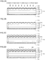
- a laser beam which falls within a visible region or within an infrared region is irradiated to the thin metal film 118 from a second main surface 114 side of the silicon carbide semiconductor base body 110 so as to heat the thin metal film 118 thus forming a metal carbide 120 on a boundary face between the silicon carbide semiconductor base body 110 and the thin metal film 118 (see Fig. 2A ).
- a laser beam which falls within a visible region for example, a green laser beam having a wavelength of 532nm
- the metal carbide 120 forms an ohmic electrode 124.
- the metal carbide 120 may be a layered metal carbide (that is, a metal carbide layer) or a granular metal carbide (that is, metal carbide grains). In both cases, the metal carbide 120 functions as the ohmic electrode 124.
- a metal containing byproduct layer 122 is formed such that the metal containing byproduct layer 122 covers the metal carbide 120 (see Fig. 2A ). Such a metal containing byproduct layer 122 can be removed in the subsequent etching step.
- silicon oxide is formed (not shown in the drawing) together with the metal containing byproduct layer 122. Such a silicon oxide film can be also removed in the subsequent etching step.
- a condition of the laser beam irradiation step is set such that the metal carbide 120 is formable on a boundary face between the silicon carbide semiconductor base body 110 and the thin metal film 118, and a temperature of a first main surface 112 side of the silicon carbide semiconductor base body 110 at the time of forming the metal carbide 120 remains at or below a maximum process temperature at the time of forming the element by a laser beam which passes through the thin metal film 118.
- the laser beam irradiation step is started under a condition that an amount of a laser beam which arrives at a depth position of 50nm from the boundary face between the silicon carbide semiconductor base body 110 and the thin metal film 118 is 10% or less, and is more preferably 1% or less.
- the metal containing byproduct layer 122 (and the silicon oxide film) which is/are possibly formed on a surface side of the metal carbide 120 is/are removed by etching using a non-oxidizing chemical solution thus exposing a surface of the metal carbide 120 (see Fig. 2B ). Due to such an operation, in the subsequent electrode forming step, a back metal (a cathode electrode 126 in this case) can be formed on the second main surface 114 of the silicon carbide semiconductor base body 110 with the metal carbide 120 (ohmic electrode 124) interposed therebetween.
- a hydrofluoric acid group chemical agent for example, a dilute hydrofluoric acid
- a cathode electrode 126 is formed on the second main surface 114 of the silicon carbide semiconductor base body 110 with the metal carbide 120 (ohmic electrode 124) interposed therebetween (see Fig. 2C ).
- the cathode electrode 126 a film formed by stacking layers of Ti, Ni and Ag is used, for example. Due to such a configuration, the back metal (the cathode electrode 126 in this case) and the silicon carbide semiconductor base body 110 are electrically connected with each other with the metal carbide 120 (ohmic electrode 124) interposed therebetween.
- the protective film 116 is removed from the first main surface 112 of the silicon carbide semiconductor base body 110 and, at the same time, an anode electrode 128 is formed on the first main surface 112 of the silicon carbide semiconductor base body 110 (see Fig. 2D ).
- Ti is favorably used for forming the anode electrode 128.
- the silicon carbide semiconductor device (pn diode) 100 according to the embodiment 1 can be manufactured by carrying out the above-mentioned steps.
- the silicon carbide semiconductor device 100 includes: the silicon carbide semiconductor base body 110 having the first main surface 112 which is an element forming surface, and the second main surface 114 which is a surface on a side opposite to the first main surface 112 and is an uneven surface; the metal carbide 120 formed (positioned) on the second main surface 114 of the silicon carbide semiconductor base body 110; the electrode layer (cathode electrode) 126 formed (positioned) on the metal carbide 120; and an anode electrode 128 formed (positioned) on the first main surface 112 of the silicon carbide semiconductor base body 110.
- the metal carbide 120 is formed by irradiating a laser beam (a green laser beam) which falls within a visible region or within an infrared region to the thin metal film 118 (Ti thin film) made of metal capable of forming metal carbide so that the ohmic electrode 124 can be formed and hence, there arises no problem on carbon precipitation.
- a laser beam a green laser beam
- Ti thin film made of metal capable of forming metal carbide
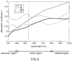
- an attenuation coefficient of the thin metal film 118 (Ti thin film) is higher in a visible region than in an ultraviolet region (see Fig. 3 ) and hence, a metal carbonization reaction can be sufficiently accelerated whereby a resistance characteristic and an adhesive characteristic of an ohmic electrode are minimally deteriorated.
- a device which irradiates a laser beam (a green laser beam) which falls within a visible region or within an infrared region is less costly than a device which irradiates a laser beam which falls within an ultraviolet region and hence, a manufacturing cost becomes low compared to a conventional method of manufacturing a silicon carbide semiconductor device.
- the method of manufacturing a silicon carbide semiconductor device according to the embodiment 1 is a method of manufacturing a silicon carbide semiconductor device capable of manufacturing an ohmic electrode having an excellent resistance characteristic and an excellent adhesive characteristic at a low manufacturing cost without causing a problem of carbon precipitation.
- the thin metal film 118 is heated not by a laser beam which falls within an ultraviolet region but by a laser beam which falls within a visible region or within an infrared region and hence, an amount of a laser beam which passes through the thin metal film 118 is decreased, and absorptivity of a laser beam by the silicon carbide semiconductor base body 110 is also decreased.
- a degree that the silicon carbide semiconductor base body 110 per se is heated by a laser beam which passes through the thin metal film 118 becomes small so that an amount of carbon generated from the silicon carbide semiconductor base body 110 can be decreased.
- the thin metal film 118 is formed of a Ti thin film. That is, metal capable of forming a metal carbide is Ti and hence, unlike the case where metal capable of forming metal carbide is W or Mo, the metal containing byproduct layer 122 (containing Ti, TiSix or the like) can be removed by etching without using an oxidizing chemical solution. As a result, a surface of the metal carbide 120 is minimally oxidized and hence, adhesiveness between the metal carbide 120 and the back metal (in this case, the cathode electrode 126) is minimally deteriorated.
- the laser beam irradiation step is performed using a green laser beam (wavelength: 532nm, a wave having a wavelength twice as large as a wavelength of YAG laser beam) having a larger attenuation coefficient for the thin metal film 118 than that of a laser beam which falls within an ultraviolet region as a laser beam which falls within a visible region or within an infrared region. Accordingly, it is possible to efficiently transform the thin metal film 118 into the metal carbide 120 by efficiently heating the thin metal film 118. Accordingly, an amount of a laser beam which arrives at the silicon carbide semiconductor base body 110 can be decreased so that the influence which the laser beam exerts on the element can be decreased.
- a Ti thin film having a film thickness which falls within a range of from 50nm to 350nm is used as the thin metal film 118 and hence, a sufficient amount of metal carbide 120 as the ohmic electrode 124 can be stably formed, and the occurrence of a phenomenon that a temperature of the element becomes high so that the element is broken can be suppressed.
- the silicon carbide semiconductor device according to the embodiment 1 can be manufactured by the method of manufacturing a silicon carbide semiconductor device according to the embodiment 1. Accordingly, it is possible to provide an inexpensive silicon carbide semiconductor device which includes an ohmic electrode having an excellent resistance characteristic and an excellent adhesive characteristic without causing a problem of carbon precipitation.
- a method of manufacturing a silicon carbide semiconductor device according to an embodiment 2 basically includes substantially the same steps as the method of manufacturing a silicon carbide semiconductor device according to the embodiment 1. However, the method of manufacturing a silicon carbide semiconductor device according to the embodiment 2 differs from the method of manufacturing a silicon carbide semiconductor device according to the embodiment 1 with respect to a point that a silicon carbide semiconductor device to be manufactured is not a pn diode but is a Schottky barrier diode.
- the method of manufacturing a silicon carbide semiconductor device according to the embodiment 2 differs from the method of manufacturing a silicon carbide semiconductor device according to the embodiment 1 with respect to the point that a silicon carbide semiconductor device to be manufactured is not a pn diode but is a Schottky barrier diode.
- a metal carbide is formed by irradiating a laser beam (a green laser beam) which falls within a visible region or within an infrared region to the thin metal film (Ti thin film) made of metal capable of forming metal carbide so that the ohmic electrode can be formed.
- the method of manufacturing a silicon carbide semiconductor device according to the embodiment 2 includes: a silicon carbide semiconductor base body preparation step; a polishing step; a thin metal film forming step; a laser beam irradiating step; an etching step; and an electrode layer forming step which are performed in this order.
- a silicon carbide semiconductor base body preparation step a polishing step; a thin metal film forming step; a laser beam irradiating step; an etching step; and an electrode layer forming step which are performed in this order.
- the method of manufacturing a silicon carbide semiconductor device according to the embodiment 2 is described in detail with reference to Fig. 4A to Fig. 5B .
- the silicon carbide semiconductor base body preparation step is a step of preparing a silicon carbide semiconductor base body which includes a first main surface forming an element forming surface and a second main surface forming a surface opposite to the first main surface.
- a silicon carbide semiconductor base body 210 is formed by stacking an n - type silicon carbide epitaxial layer 210b on an n + type silicon carbide semiconductor substrate 210a.
- a Schottky metal layer 215 which forms a Schottky junction with an n - type silicon carbide epitaxial layer 210b is formed on a first main surface 212 of the silicon carbide semiconductor base body 210.
- a peripheral withstand voltage structure not shown in the drawing is formed on the first main surface 212 of the silicon carbide semiconductor base body 210.
- a Schottky junction and the peripheral withstand voltage structure are formed on the silicon carbide semiconductor base body 210 on a first main surface 212 side, and the first main surface 212 forms an element forming surface (see Fig. 4A and Fig. 4B ).
- the Schottky junction and the peripheral withstand voltage structure correspond to the element according to the present invention.
- a protective film 216 for protecting an element is formed on the first main surface 212 of the silicon carbide semiconductor base body 210 and, thereafter, unevenness is formed on a second main surface 214 of the silicon carbide semiconductor base body 210 by polishing the silicon carbide semiconductor base body 210 from a second main surface 214 side (see Fig. 4C ).
- a thin metal film 218 made of metal capable of forming a metal carbide is formed on the second main surface 214 of the silicon carbide semiconductor base body 210 by a CVD method or a sputtering method (see Fig. 4D ).
- the thin metal film 218 is heated by irradiating a laser beam which falls within a visible region or within an infrared region to the thin metal film 218 from a second main surface 214 side of the silicon carbide semiconductor base body 210 thus forming a metal carbide 220 on a boundary face between the silicon carbide semiconductor base body 210 and the thin metal film 218 (see Fig. 5A ).
- a metal containing byproduct layer 222 (and a silicon oxide film) possibly formed on a surface side of the metal carbide 220 as described above is removed by etching using a non-oxidizing chemical solution thus exposing a surface of the metal carbide 220 (see Fig. 5B ).
- a cathode electrode 226 is formed on the second main surface 214 of the silicon carbide semiconductor base body 210 with the metal carbide 220 (ohmic electrode 224) interposed therebetween (see Fig. 5C ).
- the cathode electrode 226, a film formed by stacking layers of Ti, Ni and Ag is used, for example. Due to such a configuration, the back metal (the cathode electrode 226 in this case) and the silicon carbide semiconductor base body 210 are electrically connected with each other with the metal carbide 220 (ohmic electrode 224) interposed therebetween.
- the protective film 216 is removed from the first main surface 212 of the silicon carbide semiconductor base body 210 and, at the same time, an anode electrode 228 is formed on the first main surface 212 of the silicon carbide semiconductor base body 210 (see Fig. 5D ).
- the silicon carbide semiconductor device (Schottky barrier diode) 200 according to the embodiment 2 can be manufactured by carrying out the above-mentioned steps.
- a method of manufacturing a silicon carbide semiconductor device according to an embodiment 3 basically includes the substantially same steps as the method of manufacturing a silicon carbide semiconductor device according to the embodiment 1. However, the method of manufacturing a silicon carbide semiconductor device according to the embodiment 3 differs from the method of manufacturing a silicon carbide semiconductor device according to the embodiment 1 with respect to a point that a silicon carbide semiconductor device to be manufactured is not a pn diode but is a power MOSFET.
- the method of manufacturing a silicon carbide semiconductor device according to the embodiment 3 differs from the method of manufacturing a silicon carbide semiconductor device according to the embodiment 1 with respect to the point that a silicon carbide semiconductor device to be manufactured is not a pn diode but is a power MOSFET.
- the metal carbide is formed by irradiating a laser beam (a green laser beam) which falls within a visible region or within an infrared region to the thin metal film (Ti thin film) made of metal capable of forming a metal carbide so that the ohmic electrode can be formed.
- the method of manufacturing a silicon carbide semiconductor device according to the embodiment 3 includes, in the following order: a silicon carbide semiconductor base body preparation step; a polishing step; a thin metal film forming step; a laser beam irradiating step; an etching step; and an electrode layer forming step which are performed.
- a silicon carbide semiconductor base body preparation step a polishing step; a thin metal film forming step; a laser beam irradiating step; an etching step; and an electrode layer forming step which are performed.
- a silicon carbide semiconductor base body preparation step includes, in the following order: a silicon carbide semiconductor base body preparation step; a polishing step; a thin metal film forming step; a laser beam irradiating step; an etching step; and an electrode layer forming step which are performed.
- the method of manufacturing a silicon carbide semiconductor device according to the embodiment 3 is described in detail with reference to Fig. 6A to Fig. 7D .
- the silicon carbide semiconductor base body preparation step is a step of preparing a silicon carbide semiconductor base body 310 which includes a first main surface 312 forming an element forming surface and a second main surface 314 forming a surface on a side opposite to the first main surface 312. First, the silicon carbide semiconductor base body 310 where a p + type semiconductor layer not shown in the drawing is formed on an n - type silicon carbide semiconductor substrate on one surface (second main surface) side is prepared.
- a MOS structure not shown in the drawing (a p type body region, a p + type body contact region, an n + type source region, a gate insulation layer, a gate electrode, a protective insulation layer, a source electrode and the like) and a peripheral withstand voltage structure not shown in the drawing are formed on the silicon carbide semiconductor base body 310 on a first main surface 312 side.
- the first main surface 312 forms an element forming surface (see Fig. 6A and Fig. 6B ).
- the above-mentioned MOS structure and the peripheral withstand voltage structure correspond to the element according to the present invention.
- a thin metal film 318 made of metal capable of forming a metal carbide is formed on the second main surface 314 of the silicon carbide semiconductor base body 310 by a CVD method or a sputtering method (see Fig. 6D ).
- the thin metal film 318 is heated by irradiating a laser beam which falls within a visible region or within an infrared region to the thin metal film 318 from a second main surface 314 side of the silicon carbide semiconductor base body 310 thus forming a metal carbide 320 on a boundary face between the silicon carbide semiconductor base body 310 and the thin metal film 318 (see Fig. 7A ).
- a metal containing byproduct layer 322 (and a silicon oxide film) possibly formed on a surface side of the metal carbide 320 as described above is removed by etching using a non-oxidizing chemical solution thus exposing a surface of the metal carbide 320 (see Fig. 7B ).
- a drain electrode 326 is formed on the second main surface 314 of the silicon carbide semiconductor base body 310 with the metal carbide 320 (ohmic electrode 324) interposed therebetween (see Fig. 7C ).
- the drain electrode 326 a film formed by stacking layers of Ti, Ni and Ag is used, for example. Due to such a configuration, the back metal (the drain electrode 326 in this case) and the silicon carbide semiconductor base body 310 are electrically connected with each other with the metal carbide 320 (ohmic electrode 324) interposed therebetween.
- the protective film 316 is removed from the first main surface 312 of the silicon carbide semiconductor base body 310 and, at the same time, a source electrode 328 and a gate pad electrode not shown in the drawing are formed on the first main surface 312 of the silicon carbide semiconductor base body 310 (see Fig. 7D ).
- the silicon carbide semiconductor device (planar type MOSFET) 300 according to the embodiment 3 can be manufactured by carrying out the above-mentioned steps.
- the silicon carbide semiconductor device 300 includes: the silicon carbide semiconductor base body 310 having the first main surface 312 which is an element forming surface, and the second main surface 314 which is a surface on a side opposite to the first main surface 312 and is an uneven surface; the metal carbide 320 formed (positioned) on the second main surface 314 of the silicon carbide semiconductor base body 310; and the electrode layer (drain electrode) 326 formed (positioned) on the metal carbide 320.
- a method of manufacturing a silicon carbide semiconductor device according to an embodiment 4 basically includes substantially the same steps as the method of manufacturing a silicon carbide semiconductor device according to the embodiment 3. However, the method of manufacturing a silicon carbide semiconductor device according to the embodiment 4 differs from the method of manufacturing a silicon carbide semiconductor device according to the embodiment 3 with respect to the content of a laser beam irradiating step. That is, in the method of manufacturing a silicon carbide semiconductor device according to the embodiment 4, as shown in Fig. 8A and Fig. 8B , the laser beam irradiating step is performed under a condition that a laser beam is not irradiated onto scribe lines.
- the method of manufacturing a silicon carbide semiconductor device according to the embodiment 4 differs from the method of manufacturing a silicon carbide semiconductor device according to the embodiment 3 with respect to the content of the laser beam irradiating step.
- the metal carbide is formed by irradiating a laser beam (a green laser beam) which falls within a visible region or within an infrared region to the thin metal film (thin Ti film) made of metal capable of forming a metal carbide so that the ohmic electrode can be formed.
- the method of manufacturing a silicon carbide semiconductor device according to the embodiment 4 includes, in the following order: a silicon carbide semiconductor base body preparation step; a polishing step; a thin metal film forming step; a laser beam irradiating step; an etching step and an electrode layer forming step which are performed.
- a silicon carbide semiconductor base body preparation step a polishing step; a thin metal film forming step; a laser beam irradiating step; an etching step and an electrode layer forming step which are performed.
- the silicon carbide semiconductor base body preparation step is performed.
- the thin metal film forming step is performed (see Fig. 8A ).
- the laser beam irradiation step is performed.
- the laser beam irradiating step is performed under a condition that a laser beam is not irradiated onto scribe lines. Accordingly, in regions not including the scribe lines, in substantially the same manner as the case of the embodiment 3, a metal carbide 320 and a metal containing byproduct layer 322 are formed on a silicon carbide semiconductor base body 310. On the scribe lines, a thin metal film 318 remains on the silicon carbide semiconductor base body 310 as it is.
- the metal containing byproduct layer 322 (and a silicon oxide film) is removed by etching using a non-oxidizing chemical solution thus exposing a surface of the metal carbide 320.
- the thin metal film 318 is also removed by etching using a non-oxidizing chemical solution (see Fig. 8C ).
- the electrode layer forming step is performed (see Fig. 9A and Fig. 9B ).
- a wafer-shaped silicon carbide semiconductor device (planar-type MOSFET) 302 can be manufactured.
- chip-shaped silicon carbide semiconductor devices 304 can be manufactured.
- a metal carbide is not present on the scribe lines and hence, an operation of cutting and dividing the wafer-shaped silicon carbide semiconductor device 102 can be easily performed.
Landscapes
- Electrodes Of Semiconductors (AREA)
- Physics & Mathematics (AREA)
- Electromagnetism (AREA)
- Optics & Photonics (AREA)
Applications Claiming Priority (1)
| Application Number | Priority Date | Filing Date | Title |
|---|---|---|---|
| PCT/JP2015/072883 WO2017026068A1 (ja) | 2015-08-12 | 2015-08-12 | 炭化珪素半導体装置の製造方法及び炭化珪素半導体装置 |
Publications (3)
| Publication Number | Publication Date |
|---|---|
| EP3336879A1 true EP3336879A1 (de) | 2018-06-20 |
| EP3336879A4 EP3336879A4 (de) | 2019-04-03 |
| EP3336879B1 EP3336879B1 (de) | 2020-03-25 |
Family
ID=57984226
Family Applications (1)
| Application Number | Title | Priority Date | Filing Date |
|---|---|---|---|
| EP15889428.7A Active EP3336879B1 (de) | 2015-08-12 | 2015-08-12 | Verfahren zur herstellung eines siliziumkarbidhalbleiterbauelements |
Country Status (6)
| Country | Link |
|---|---|
| US (1) | US10403497B2 (de) |
| EP (1) | EP3336879B1 (de) |
| JP (1) | JP6165313B2 (de) |
| CN (1) | CN106575610B (de) |
| TW (1) | TWI600066B (de) |
| WO (1) | WO2017026068A1 (de) |
Families Citing this family (4)
| Publication number | Priority date | Publication date | Assignee | Title |
|---|---|---|---|---|
| WO2017104751A1 (ja) | 2015-12-18 | 2017-06-22 | 富士電機株式会社 | 炭化珪素半導体基板、炭化珪素半導体基板の製造方法、半導体装置および半導体装置の製造方法 |
| JP7225873B2 (ja) * | 2019-02-07 | 2023-02-21 | 富士電機株式会社 | 半導体装置及び半導体装置の製造方法 |
| JP7314758B2 (ja) * | 2019-10-11 | 2023-07-26 | 株式会社デンソー | 炭化珪素半導体装置およびその製造方法 |
| CN113809183A (zh) * | 2020-06-11 | 2021-12-17 | 珠海格力电器股份有限公司 | 一种mps二极管器件及其制备方法 |
Family Cites Families (21)
| Publication number | Priority date | Publication date | Assignee | Title |
|---|---|---|---|---|
| JP3871607B2 (ja) * | 2001-12-14 | 2007-01-24 | 松下電器産業株式会社 | 半導体素子およびその製造方法 |
| US20050104072A1 (en) | 2003-08-14 | 2005-05-19 | Slater David B.Jr. | Localized annealing of metal-silicon carbide ohmic contacts and devices so formed |
| US7337956B2 (en) * | 2004-04-12 | 2008-03-04 | Rearden Capital Corporation | System and method for facilitating the purchase of goods and services |
| JP2006024880A (ja) * | 2004-06-09 | 2006-01-26 | Matsushita Electric Ind Co Ltd | 半導体装置及びその製造方法 |
| US7598516B2 (en) * | 2005-01-07 | 2009-10-06 | International Business Machines Corporation | Self-aligned process for nanotube/nanowire FETs |
| JP2008135611A (ja) * | 2006-11-29 | 2008-06-12 | Denso Corp | 半導体装置の製造方法 |
| JP5460975B2 (ja) | 2008-05-23 | 2014-04-02 | 株式会社デンソー | 半導体装置の製造方法 |
| JP5369762B2 (ja) * | 2009-03-02 | 2013-12-18 | 株式会社デンソー | 炭化珪素半導体装置の製造方法 |
| JP2011071302A (ja) * | 2009-09-25 | 2011-04-07 | Toshiba Corp | 不揮発性記憶装置の製造方法および不揮発性記憶装置 |
| JP4924690B2 (ja) | 2009-10-20 | 2012-04-25 | 株式会社デンソー | 炭化珪素半導体装置の製造方法 |
| JP5482107B2 (ja) * | 2009-10-30 | 2014-04-23 | 株式会社デンソー | 炭化珪素半導体装置の製造方法 |
| JP2011146622A (ja) * | 2010-01-18 | 2011-07-28 | Mitsubishi Electric Corp | 炭化珪素半導体装置の製造方法 |
| JP2012004185A (ja) * | 2010-06-14 | 2012-01-05 | Denso Corp | 炭化珪素半導体装置の製造方法 |
| JP6099298B2 (ja) * | 2011-05-30 | 2017-03-22 | 富士電機株式会社 | SiC半導体デバイス及びその製造方法 |
| JP5464192B2 (ja) * | 2011-09-29 | 2014-04-09 | 株式会社デンソー | 半導体装置の製造方法 |
| US8557631B2 (en) * | 2011-12-01 | 2013-10-15 | Taiwan Semiconductor Manufacturing Co., Ltd. | Interposer wafer bonding method and apparatus |
| JP6112698B2 (ja) * | 2012-03-30 | 2017-04-12 | 富士電機株式会社 | 炭化珪素半導体素子及びその製造方法 |
| JP6051573B2 (ja) * | 2012-04-17 | 2016-12-27 | 富士電機株式会社 | 半導体装置の製造方法 |
| JP2014107345A (ja) * | 2012-11-26 | 2014-06-09 | Mitsubishi Electric Corp | 炭化珪素ショットキバリアダイオードの製造方法 |
| JP5962475B2 (ja) * | 2012-12-06 | 2016-08-03 | 三菱電機株式会社 | 炭化珪素半導体装置の製造方法及び炭化珪素半導体装置 |
| JP6034694B2 (ja) * | 2012-12-30 | 2016-11-30 | 新電元工業株式会社 | 半導体装置の製造方法及び半導体装置 |
-
2015
- 2015-08-12 EP EP15889428.7A patent/EP3336879B1/de active Active
- 2015-08-12 US US15/314,471 patent/US10403497B2/en active Active
- 2015-08-12 JP JP2016503041A patent/JP6165313B2/ja active Active
- 2015-08-12 CN CN201580007867.2A patent/CN106575610B/zh active Active
- 2015-08-12 WO PCT/JP2015/072883 patent/WO2017026068A1/ja not_active Ceased
-
2016
- 2016-08-12 TW TW105125738A patent/TWI600066B/zh active
Also Published As
| Publication number | Publication date |
|---|---|
| CN106575610A (zh) | 2017-04-19 |
| TWI600066B (zh) | 2017-09-21 |
| JPWO2017026068A1 (ja) | 2017-08-10 |
| US20180174835A1 (en) | 2018-06-21 |
| WO2017026068A1 (ja) | 2017-02-16 |
| EP3336879B1 (de) | 2020-03-25 |
| JP6165313B2 (ja) | 2017-07-19 |
| US10403497B2 (en) | 2019-09-03 |
| CN106575610B (zh) | 2019-12-24 |
| TW201707074A (zh) | 2017-02-16 |
| EP3336879A4 (de) | 2019-04-03 |
Similar Documents
| Publication | Publication Date | Title |
|---|---|---|
| US8823017B2 (en) | Semiconductor device and method of manufacturing the same | |
| US8216929B2 (en) | Method of manufacturing silicon carbide semiconductor device | |
| US9240451B2 (en) | Silicon carbide semiconductor device | |
| US9263525B2 (en) | Silicon carbide semiconductor device and manufacturing method thereof | |
| DE102016216521B4 (de) | Verfahren zum Herstellen einer Halbleiteranordnung | |
| CN105308722B (zh) | 碳化硅半导体装置及碳化硅半导体装置的制造方法 | |
| US9159792B2 (en) | SiC semiconductor device and method for manufacturing the same | |
| EP3336879A1 (de) | Verfahren zur herstellung eines siliciumcarbidhalbleiterbauelements sowie siliciumcarbidhalbleiterbauelement | |
| JP2017118060A (ja) | 半導体装置および半導体装置の製造方法 | |
| US11387326B2 (en) | Silicon carbide semiconductor device and method for manufacturing the same | |
| CN103069546B (zh) | 半导体器件的制造方法 | |
| US9543154B2 (en) | Method for manufacturing semiconductor device | |
| EP2905806B1 (de) | Herstellungsverfahren für ein siliciumcarbidhalbleiterbauelement | |
| US10050133B2 (en) | Application of thin insulating film layer in semiconductor device and method of manufacturing semiconductor device | |
| JP6442800B2 (ja) | 半導体装置及び半導体装置を製造する方法 | |
| US20250194209A1 (en) | Semiconductor device | |
| JP6918902B2 (ja) | 半導体装置の製造方法 | |
| US9018049B2 (en) | Method for manufacturing insulated gate bipolar transistor IGBT | |
| JP2018049927A (ja) | 炭化珪素半導体装置およびその製造方法 |
Legal Events
| Date | Code | Title | Description |
|---|---|---|---|
| STAA | Information on the status of an ep patent application or granted ep patent |
Free format text: STATUS: UNKNOWN |
|
| STAA | Information on the status of an ep patent application or granted ep patent |
Free format text: STATUS: THE INTERNATIONAL PUBLICATION HAS BEEN MADE |
|
| PUAI | Public reference made under article 153(3) epc to a published international application that has entered the european phase |
Free format text: ORIGINAL CODE: 0009012 |
|
| STAA | Information on the status of an ep patent application or granted ep patent |
Free format text: STATUS: REQUEST FOR EXAMINATION WAS MADE |
|
| 17P | Request for examination filed |
Effective date: 20161025 |
|
| AK | Designated contracting states |
Kind code of ref document: A1 Designated state(s): AL AT BE BG CH CY CZ DE DK EE ES FI FR GB GR HR HU IE IS IT LI LT LU LV MC MK MT NL NO PL PT RO RS SE SI SK SM TR |
|
| AX | Request for extension of the european patent |
Extension state: BA ME |
|
| DAV | Request for validation of the european patent (deleted) | ||
| DAX | Request for extension of the european patent (deleted) | ||
| A4 | Supplementary search report drawn up and despatched |
Effective date: 20190301 |
|
| RIC1 | Information provided on ipc code assigned before grant |
Ipc: H01L 21/28 20060101AFI20190225BHEP Ipc: H01L 21/428 20060101ALI20190225BHEP Ipc: H01L 29/45 20060101ALI20190225BHEP Ipc: H01L 29/868 20060101ALI20190225BHEP Ipc: H01L 21/329 20060101ALI20190225BHEP Ipc: H01L 21/268 20060101ALI20190225BHEP Ipc: H01L 29/78 20060101ALI20190225BHEP Ipc: H01L 21/04 20060101ALI20190225BHEP |
|
| RIC1 | Information provided on ipc code assigned before grant |
Ipc: H01L 29/45 20060101ALI20190917BHEP Ipc: H01L 29/78 20060101ALI20190917BHEP Ipc: H01L 29/872 20060101ALI20190917BHEP Ipc: H01L 21/329 20060101ALI20190917BHEP Ipc: H01L 21/04 20060101ALI20190917BHEP Ipc: H01L 29/06 20060101ALI20190917BHEP Ipc: H01L 21/28 20060101AFI20190917BHEP Ipc: H01L 29/34 20060101ALI20190917BHEP Ipc: H01L 29/861 20060101ALI20190917BHEP Ipc: H01L 29/66 20060101ALI20190917BHEP Ipc: H01L 21/268 20060101ALI20190917BHEP Ipc: H01L 29/868 20060101ALI20190917BHEP Ipc: H01L 21/428 20060101ALI20190917BHEP Ipc: H01L 29/16 20060101ALI20190917BHEP |
|
| GRAP | Despatch of communication of intention to grant a patent |
Free format text: ORIGINAL CODE: EPIDOSNIGR1 |
|
| STAA | Information on the status of an ep patent application or granted ep patent |
Free format text: STATUS: GRANT OF PATENT IS INTENDED |
|
| INTG | Intention to grant announced |
Effective date: 20191031 |
|
| GRAS | Grant fee paid |
Free format text: ORIGINAL CODE: EPIDOSNIGR3 |
|
| GRAA | (expected) grant |
Free format text: ORIGINAL CODE: 0009210 |
|
| STAA | Information on the status of an ep patent application or granted ep patent |
Free format text: STATUS: THE PATENT HAS BEEN GRANTED |
|
| AK | Designated contracting states |
Kind code of ref document: B1 Designated state(s): AL AT BE BG CH CY CZ DE DK EE ES FI FR GB GR HR HU IE IS IT LI LT LU LV MC MK MT NL NO PL PT RO RS SE SI SK SM TR |
|
| REG | Reference to a national code |
Ref country code: GB Ref legal event code: FG4D |
|
| REG | Reference to a national code |
Ref country code: AT Ref legal event code: REF Ref document number: 1249551 Country of ref document: AT Kind code of ref document: T Effective date: 20200415 Ref country code: IE Ref legal event code: FG4D |
|
| REG | Reference to a national code |
Ref country code: DE Ref legal event code: R096 Ref document number: 602015049627 Country of ref document: DE |
|
| PG25 | Lapsed in a contracting state [announced via postgrant information from national office to epo] |
Ref country code: FI Free format text: LAPSE BECAUSE OF FAILURE TO SUBMIT A TRANSLATION OF THE DESCRIPTION OR TO PAY THE FEE WITHIN THE PRESCRIBED TIME-LIMIT Effective date: 20200325 Ref country code: NO Free format text: LAPSE BECAUSE OF FAILURE TO SUBMIT A TRANSLATION OF THE DESCRIPTION OR TO PAY THE FEE WITHIN THE PRESCRIBED TIME-LIMIT Effective date: 20200625 Ref country code: RS Free format text: LAPSE BECAUSE OF FAILURE TO SUBMIT A TRANSLATION OF THE DESCRIPTION OR TO PAY THE FEE WITHIN THE PRESCRIBED TIME-LIMIT Effective date: 20200325 |
|
| PG25 | Lapsed in a contracting state [announced via postgrant information from national office to epo] |
Ref country code: LV Free format text: LAPSE BECAUSE OF FAILURE TO SUBMIT A TRANSLATION OF THE DESCRIPTION OR TO PAY THE FEE WITHIN THE PRESCRIBED TIME-LIMIT Effective date: 20200325 Ref country code: SE Free format text: LAPSE BECAUSE OF FAILURE TO SUBMIT A TRANSLATION OF THE DESCRIPTION OR TO PAY THE FEE WITHIN THE PRESCRIBED TIME-LIMIT Effective date: 20200325 Ref country code: HR Free format text: LAPSE BECAUSE OF FAILURE TO SUBMIT A TRANSLATION OF THE DESCRIPTION OR TO PAY THE FEE WITHIN THE PRESCRIBED TIME-LIMIT Effective date: 20200325 Ref country code: GR Free format text: LAPSE BECAUSE OF FAILURE TO SUBMIT A TRANSLATION OF THE DESCRIPTION OR TO PAY THE FEE WITHIN THE PRESCRIBED TIME-LIMIT Effective date: 20200626 Ref country code: BG Free format text: LAPSE BECAUSE OF FAILURE TO SUBMIT A TRANSLATION OF THE DESCRIPTION OR TO PAY THE FEE WITHIN THE PRESCRIBED TIME-LIMIT Effective date: 20200625 |
|
| REG | Reference to a national code |
Ref country code: NL Ref legal event code: MP Effective date: 20200325 |
|
| REG | Reference to a national code |
Ref country code: LT Ref legal event code: MG4D |
|
| PG25 | Lapsed in a contracting state [announced via postgrant information from national office to epo] |
Ref country code: NL Free format text: LAPSE BECAUSE OF FAILURE TO SUBMIT A TRANSLATION OF THE DESCRIPTION OR TO PAY THE FEE WITHIN THE PRESCRIBED TIME-LIMIT Effective date: 20200325 |
|
| PG25 | Lapsed in a contracting state [announced via postgrant information from national office to epo] |
Ref country code: SM Free format text: LAPSE BECAUSE OF FAILURE TO SUBMIT A TRANSLATION OF THE DESCRIPTION OR TO PAY THE FEE WITHIN THE PRESCRIBED TIME-LIMIT Effective date: 20200325 Ref country code: EE Free format text: LAPSE BECAUSE OF FAILURE TO SUBMIT A TRANSLATION OF THE DESCRIPTION OR TO PAY THE FEE WITHIN THE PRESCRIBED TIME-LIMIT Effective date: 20200325 Ref country code: LT Free format text: LAPSE BECAUSE OF FAILURE TO SUBMIT A TRANSLATION OF THE DESCRIPTION OR TO PAY THE FEE WITHIN THE PRESCRIBED TIME-LIMIT Effective date: 20200325 Ref country code: RO Free format text: LAPSE BECAUSE OF FAILURE TO SUBMIT A TRANSLATION OF THE DESCRIPTION OR TO PAY THE FEE WITHIN THE PRESCRIBED TIME-LIMIT Effective date: 20200325 Ref country code: PT Free format text: LAPSE BECAUSE OF FAILURE TO SUBMIT A TRANSLATION OF THE DESCRIPTION OR TO PAY THE FEE WITHIN THE PRESCRIBED TIME-LIMIT Effective date: 20200818 Ref country code: CZ Free format text: LAPSE BECAUSE OF FAILURE TO SUBMIT A TRANSLATION OF THE DESCRIPTION OR TO PAY THE FEE WITHIN THE PRESCRIBED TIME-LIMIT Effective date: 20200325 Ref country code: SK Free format text: LAPSE BECAUSE OF FAILURE TO SUBMIT A TRANSLATION OF THE DESCRIPTION OR TO PAY THE FEE WITHIN THE PRESCRIBED TIME-LIMIT Effective date: 20200325 Ref country code: IS Free format text: LAPSE BECAUSE OF FAILURE TO SUBMIT A TRANSLATION OF THE DESCRIPTION OR TO PAY THE FEE WITHIN THE PRESCRIBED TIME-LIMIT Effective date: 20200725 |
|
| REG | Reference to a national code |
Ref country code: AT Ref legal event code: MK05 Ref document number: 1249551 Country of ref document: AT Kind code of ref document: T Effective date: 20200325 |
|
| REG | Reference to a national code |
Ref country code: DE Ref legal event code: R097 Ref document number: 602015049627 Country of ref document: DE |
|
| PG25 | Lapsed in a contracting state [announced via postgrant information from national office to epo] |
Ref country code: ES Free format text: LAPSE BECAUSE OF FAILURE TO SUBMIT A TRANSLATION OF THE DESCRIPTION OR TO PAY THE FEE WITHIN THE PRESCRIBED TIME-LIMIT Effective date: 20200325 Ref country code: AT Free format text: LAPSE BECAUSE OF FAILURE TO SUBMIT A TRANSLATION OF THE DESCRIPTION OR TO PAY THE FEE WITHIN THE PRESCRIBED TIME-LIMIT Effective date: 20200325 Ref country code: DK Free format text: LAPSE BECAUSE OF FAILURE TO SUBMIT A TRANSLATION OF THE DESCRIPTION OR TO PAY THE FEE WITHIN THE PRESCRIBED TIME-LIMIT Effective date: 20200325 |
|
| PLBE | No opposition filed within time limit |
Free format text: ORIGINAL CODE: 0009261 |
|
| STAA | Information on the status of an ep patent application or granted ep patent |
Free format text: STATUS: NO OPPOSITION FILED WITHIN TIME LIMIT |
|
| PG25 | Lapsed in a contracting state [announced via postgrant information from national office to epo] |
Ref country code: PL Free format text: LAPSE BECAUSE OF FAILURE TO SUBMIT A TRANSLATION OF THE DESCRIPTION OR TO PAY THE FEE WITHIN THE PRESCRIBED TIME-LIMIT Effective date: 20200325 |
|
| 26N | No opposition filed |
Effective date: 20210112 |
|
| PG25 | Lapsed in a contracting state [announced via postgrant information from national office to epo] |
Ref country code: MC Free format text: LAPSE BECAUSE OF FAILURE TO SUBMIT A TRANSLATION OF THE DESCRIPTION OR TO PAY THE FEE WITHIN THE PRESCRIBED TIME-LIMIT Effective date: 20200325 |
|
| REG | Reference to a national code |
Ref country code: CH Ref legal event code: PL |
|
| GBPC | Gb: european patent ceased through non-payment of renewal fee |
Effective date: 20200812 |
|
| PG25 | Lapsed in a contracting state [announced via postgrant information from national office to epo] |
Ref country code: CH Free format text: LAPSE BECAUSE OF NON-PAYMENT OF DUE FEES Effective date: 20200831 Ref country code: LU Free format text: LAPSE BECAUSE OF NON-PAYMENT OF DUE FEES Effective date: 20200812 Ref country code: LI Free format text: LAPSE BECAUSE OF NON-PAYMENT OF DUE FEES Effective date: 20200831 |
|
| REG | Reference to a national code |
Ref country code: BE Ref legal event code: MM Effective date: 20200831 |
|
| PG25 | Lapsed in a contracting state [announced via postgrant information from national office to epo] |
Ref country code: SI Free format text: LAPSE BECAUSE OF FAILURE TO SUBMIT A TRANSLATION OF THE DESCRIPTION OR TO PAY THE FEE WITHIN THE PRESCRIBED TIME-LIMIT Effective date: 20200325 |
|
| PG25 | Lapsed in a contracting state [announced via postgrant information from national office to epo] |
Ref country code: FR Free format text: LAPSE BECAUSE OF NON-PAYMENT OF DUE FEES Effective date: 20200831 |
|
| PG25 | Lapsed in a contracting state [announced via postgrant information from national office to epo] |
Ref country code: GB Free format text: LAPSE BECAUSE OF NON-PAYMENT OF DUE FEES Effective date: 20200812 Ref country code: IE Free format text: LAPSE BECAUSE OF NON-PAYMENT OF DUE FEES Effective date: 20200812 Ref country code: BE Free format text: LAPSE BECAUSE OF NON-PAYMENT OF DUE FEES Effective date: 20200831 |
|
| PG25 | Lapsed in a contracting state [announced via postgrant information from national office to epo] |
Ref country code: TR Free format text: LAPSE BECAUSE OF FAILURE TO SUBMIT A TRANSLATION OF THE DESCRIPTION OR TO PAY THE FEE WITHIN THE PRESCRIBED TIME-LIMIT Effective date: 20200325 Ref country code: MT Free format text: LAPSE BECAUSE OF FAILURE TO SUBMIT A TRANSLATION OF THE DESCRIPTION OR TO PAY THE FEE WITHIN THE PRESCRIBED TIME-LIMIT Effective date: 20200325 Ref country code: CY Free format text: LAPSE BECAUSE OF FAILURE TO SUBMIT A TRANSLATION OF THE DESCRIPTION OR TO PAY THE FEE WITHIN THE PRESCRIBED TIME-LIMIT Effective date: 20200325 |
|
| PG25 | Lapsed in a contracting state [announced via postgrant information from national office to epo] |
Ref country code: MK Free format text: LAPSE BECAUSE OF FAILURE TO SUBMIT A TRANSLATION OF THE DESCRIPTION OR TO PAY THE FEE WITHIN THE PRESCRIBED TIME-LIMIT Effective date: 20200325 Ref country code: AL Free format text: LAPSE BECAUSE OF FAILURE TO SUBMIT A TRANSLATION OF THE DESCRIPTION OR TO PAY THE FEE WITHIN THE PRESCRIBED TIME-LIMIT Effective date: 20200325 |
|
| REG | Reference to a national code |
Ref country code: DE Ref legal event code: R079 Ref document number: 602015049627 Country of ref document: DE Free format text: PREVIOUS MAIN CLASS: H01L0021280000 Ipc: H10D0064010000 |
|
| PGFP | Annual fee paid to national office [announced via postgrant information from national office to epo] |
Ref country code: DE Payment date: 20250820 Year of fee payment: 11 |
|
| PGFP | Annual fee paid to national office [announced via postgrant information from national office to epo] |
Ref country code: IT Payment date: 20250825 Year of fee payment: 11 |