EP3338149B1 - Méthode d'exploitation d'un distributeur de courant et distributeur de courant - Google Patents
Méthode d'exploitation d'un distributeur de courant et distributeur de courant Download PDFInfo
- Publication number
- EP3338149B1 EP3338149B1 EP16753294.4A EP16753294A EP3338149B1 EP 3338149 B1 EP3338149 B1 EP 3338149B1 EP 16753294 A EP16753294 A EP 16753294A EP 3338149 B1 EP3338149 B1 EP 3338149B1
- Authority
- EP
- European Patent Office
- Prior art keywords
- controller
- module
- connection
- contact
- modules
- Prior art date
- Legal status (The legal status is an assumption and is not a legal conclusion. Google has not performed a legal analysis and makes no representation as to the accuracy of the status listed.)
- Active
Links
Images





Classifications
-
- E—FIXED CONSTRUCTIONS
- E04—BUILDING
- E04F—FINISHING WORK ON BUILDINGS, e.g. STAIRS, FLOORS
- E04F21/00—Implements for finishing work on buildings
- E04F21/18—Implements for finishing work on buildings for setting wall or ceiling slabs or plates
-
- G—PHYSICS
- G01—MEASURING; TESTING
- G01R—MEASURING ELECTRIC VARIABLES; MEASURING MAGNETIC VARIABLES
- G01R31/00—Arrangements for testing electric properties; Arrangements for locating electric faults; Arrangements for electrical testing characterised by what is being tested not provided for elsewhere
- G01R31/50—Testing of electric apparatus, lines, cables or components for short-circuits, continuity, leakage current or incorrect line connections
- G01R31/52—Testing for short-circuits, leakage current or ground faults
-
- G—PHYSICS
- G01—MEASURING; TESTING
- G01R—MEASURING ELECTRIC VARIABLES; MEASURING MAGNETIC VARIABLES
- G01R31/00—Arrangements for testing electric properties; Arrangements for locating electric faults; Arrangements for electrical testing characterised by what is being tested not provided for elsewhere
- G01R31/50—Testing of electric apparatus, lines, cables or components for short-circuits, continuity, leakage current or incorrect line connections
- G01R31/54—Testing for continuity
-
- G—PHYSICS
- G05—CONTROLLING; REGULATING
- G05B—CONTROL OR REGULATING SYSTEMS IN GENERAL; FUNCTIONAL ELEMENTS OF SUCH SYSTEMS; MONITORING OR TESTING ARRANGEMENTS FOR SUCH SYSTEMS OR ELEMENTS
- G05B19/00—Program-control systems
- G05B19/02—Program-control systems electric
- G05B19/04—Program control other than numerical control, i.e. in sequence controllers or logic controllers
- G05B19/042—Program control other than numerical control, i.e. in sequence controllers or logic controllers using digital processors
- G05B19/0421—Multiprocessor system
-
- G—PHYSICS
- G05—CONTROLLING; REGULATING
- G05B—CONTROL OR REGULATING SYSTEMS IN GENERAL; FUNCTIONAL ELEMENTS OF SUCH SYSTEMS; MONITORING OR TESTING ARRANGEMENTS FOR SUCH SYSTEMS OR ELEMENTS
- G05B19/00—Program-control systems
- G05B19/02—Program-control systems electric
- G05B19/04—Program control other than numerical control, i.e. in sequence controllers or logic controllers
- G05B19/042—Program control other than numerical control, i.e. in sequence controllers or logic controllers using digital processors
- G05B19/0423—Input/output
- G05B19/0425—Safety, monitoring
-
- H—ELECTRICITY
- H02—GENERATION; CONVERSION OR DISTRIBUTION OF ELECTRIC POWER
- H02B—BOARDS, SUBSTATIONS OR SWITCHING ARRANGEMENTS FOR THE SUPPLY OR DISTRIBUTION OF ELECTRIC POWER
- H02B1/00—Frameworks, boards, panels, desks, casings; Details of substations or switching arrangements
- H02B1/015—Boards, panels, desks; Parts thereof or accessories therefor
- H02B1/04—Mounting thereon of switches or of other devices in general, the switch or device having, or being without, casing
- H02B1/052—Mounting on rails
-
- H—ELECTRICITY
- H02—GENERATION; CONVERSION OR DISTRIBUTION OF ELECTRIC POWER
- H02B—BOARDS, SUBSTATIONS OR SWITCHING ARRANGEMENTS FOR THE SUPPLY OR DISTRIBUTION OF ELECTRIC POWER
- H02B1/00—Frameworks, boards, panels, desks, casings; Details of substations or switching arrangements
- H02B1/015—Boards, panels, desks; Parts thereof or accessories therefor
- H02B1/04—Mounting thereon of switches or of other devices in general, the switch or device having, or being without, casing
- H02B1/056—Mounting on plugboards
-
- H—ELECTRICITY
- H02—GENERATION; CONVERSION OR DISTRIBUTION OF ELECTRIC POWER
- H02B—BOARDS, SUBSTATIONS OR SWITCHING ARRANGEMENTS FOR THE SUPPLY OR DISTRIBUTION OF ELECTRIC POWER
- H02B1/00—Frameworks, boards, panels, desks, casings; Details of substations or switching arrangements
- H02B1/20—Bus-bar or other wiring layouts, e.g. in cubicles, in switchyards
- H02B1/205—Bus-bar or other wiring layouts, e.g. in cubicles, in switchyards for connecting electrical apparatus mounted side by side on a rail
-
- H—ELECTRICITY
- H02—GENERATION; CONVERSION OR DISTRIBUTION OF ELECTRIC POWER
- H02J—ELECTRIC POWER NETWORKS; CIRCUIT ARRANGEMENTS OR SYSTEMS FOR SUPPLYING OR DISTRIBUTING ELECTRIC POWER; SYSTEMS FOR STORING ELECTRIC ENERGY
- H02J13/00—Circuit arrangements for providing remote monitoring or remote control of equipment in a power distribution network
- H02J13/13—Circuit arrangements for providing remote monitoring or remote control of equipment in a power distribution network characterised by the transmission of data to equipment in the power network
- H02J13/1317—Circuit arrangements for providing remote monitoring or remote control of equipment in a power distribution network characterised by the transmission of data to equipment in the power network using an auxiliary transmission line
-
- H—ELECTRICITY
- H02—GENERATION; CONVERSION OR DISTRIBUTION OF ELECTRIC POWER
- H02J—ELECTRIC POWER NETWORKS; CIRCUIT ARRANGEMENTS OR SYSTEMS FOR SUPPLYING OR DISTRIBUTING ELECTRIC POWER; SYSTEMS FOR STORING ELECTRIC ENERGY
- H02J13/00—Circuit arrangements for providing remote monitoring or remote control of equipment in a power distribution network
- H02J13/18—Circuit arrangements for providing remote monitoring or remote control of equipment in a power distribution network characterised by the remotely-controlled equipment, e.g. converters or transformers
- H02J13/333—Circuit arrangements for providing remote monitoring or remote control of equipment in a power distribution network characterised by the remotely-controlled equipment, e.g. converters or transformers the equipment forming part of substations
-
- E—FIXED CONSTRUCTIONS
- E04—BUILDING
- E04B—GENERAL BUILDING CONSTRUCTIONS; WALLS, e.g. PARTITIONS; ROOFS; FLOORS; CEILINGS; INSULATION OR OTHER PROTECTION OF BUILDINGS
- E04B2/00—Walls, e.g. partitions, for buildings; Wall construction with regard to insulation; Connections specially adapted to walls
- E04B2/88—Curtain walls
-
- E—FIXED CONSTRUCTIONS
- E04—BUILDING
- E04F—FINISHING WORK ON BUILDINGS, e.g. STAIRS, FLOORS
- E04F13/00—Coverings or linings, e.g. for walls or ceilings
- E04F13/07—Coverings or linings, e.g. for walls or ceilings composed of covering or lining elements; Sub-structures therefor; Fastening means therefor
- E04F13/08—Coverings or linings, e.g. for walls or ceilings composed of covering or lining elements; Sub-structures therefor; Fastening means therefor composed of a plurality of similar covering or lining elements
- E04F13/0801—Separate fastening elements
- E04F13/0803—Separate fastening elements with load-supporting elongated furring elements between wall and covering elements
-
- G—PHYSICS
- G05—CONTROLLING; REGULATING
- G05B—CONTROL OR REGULATING SYSTEMS IN GENERAL; FUNCTIONAL ELEMENTS OF SUCH SYSTEMS; MONITORING OR TESTING ARRANGEMENTS FOR SUCH SYSTEMS OR ELEMENTS
- G05B2219/00—Program-control systems
- G05B2219/20—Pc systems
- G05B2219/21—Pc I-O input output
- G05B2219/21008—Read in analog values by microprocessor, potentiometer, resistor taps
-
- G—PHYSICS
- G05—CONTROLLING; REGULATING
- G05B—CONTROL OR REGULATING SYSTEMS IN GENERAL; FUNCTIONAL ELEMENTS OF SUCH SYSTEMS; MONITORING OR TESTING ARRANGEMENTS FOR SUCH SYSTEMS OR ELEMENTS
- G05B2219/00—Program-control systems
- G05B2219/20—Pc systems
- G05B2219/21—Pc I-O input output
- G05B2219/21028—Address of module determined by position
-
- G—PHYSICS
- G05—CONTROLLING; REGULATING
- G05B—CONTROL OR REGULATING SYSTEMS IN GENERAL; FUNCTIONAL ELEMENTS OF SUCH SYSTEMS; MONITORING OR TESTING ARRANGEMENTS FOR SUCH SYSTEMS OR ELEMENTS
- G05B2219/00—Program-control systems
- G05B2219/20—Pc systems
- G05B2219/25—Pc structure of the system
- G05B2219/25117—Resistors, value, combination defines a digital value
-
- H—ELECTRICITY
- H01—ELECTRIC ELEMENTS
- H01H—ELECTRIC SWITCHES; RELAYS; SELECTORS; EMERGENCY PROTECTIVE DEVICES
- H01H71/00—Details of the protective switches or relays covered by groups H01H73/00 - H01H83/00
- H01H71/02—Housings; Casings; Bases; Mountings
Definitions
- the invention relates to a method for operating a power distributor with a number of connected connection modules.
- the invention further relates to a modular power distributor for direct mounting on a mounting rail, comprising a number of power distribution modules, in particular in the form of DIN rail mounted devices.
- an electrical installation with one or more electrical load circuits, to which a current is supplied from a common main current line, will be referred to below as the current distributor.
- the current distributor As part of the power distribution fuse mechanisms are provided which protect each load circuit individually against overload and / or short circuit.
- the safety mechanisms are in particular mechanical, electronic or mechatronic circuit breakers, which are connected between a main circuit or a feed and the load circuits.
- the circuit breakers are often single wired through flexible wires to the feed and load.
- the installation of such a power distributor is particularly labor-intensive.
- the switching system formed by such a power distribution is relatively confusing due to the individual wiring, which complicates repairs and subsequent changes in the mounting state of the power distribution disadvantageous.
- Such power distributors are made of several individual and mutually electrically conductive coupled Power distribution modules composed.
- the power distribution modules are typically next to each other directly mounted as DIN rail mounted devices (DIN rail) and have on the one hand connections for a feed and for the load and on the other hand at least one socket-like slot for the interposition of a circuit breaker.
- the juxtaposed modules are typically coupled by means of a plurality of modules bridging conductor rail optically clear to each other electrically conductive.
- circuit breaker power distribution modules are provided in particular at the branches, where the load circuits branch off from the main power line.
- the circuit breakers serve to separate the respective associated load circuit in case of need from the current-carrying main power line.
- NC and NO integrated signal contacts
- connection modules with side coupling contacts for electrical or signal-technical contact connection with at least one bayed further connection module known. Between two coupling contacts, a base resistor is connected in each case such that the base resistors of the juxtaposed connection modules form a resistor chain connected in series.
- the connection modules can be equipped with an actuatable circuit breaker, which have an internal switch controller for detecting a voltage dropping to the respectively assigned socket resistor.
- each circuit breaker or each power distribution module is assigned its own signal or device address, so that each circuit breaker in the course of a signal bus individually responsive, ie in particular is controllable.
- the address assignment also takes empty slots of the modules, so that if a circuit breaker is plugged in subsequently, no new address assignment must be made.
- the invention has for its object to provide a suitable method for operating a suitable with regard to a communication and / or signaling application power distribution. Furthermore, a suitable for carrying out the process power distribution is to be specified.
- the power distributor is modular with a number of juxtaposed or stackable connection modules - hereinafter abbreviated as modules called - constructed.
- the individual modules and thus the power distribution are suitable for direct mounting on a mounting rail, such as a hat or G-rail and set up.
- the modules are for this purpose in particular in the manner of DIN rail mounted devices in a row next to each other mounted on the mounting rail.
- the module package formed thereby is connected to a common first controller (that is, to a common first controller).
- the modules each have a number of lateral coupling contacts for electrical and / or signal-technical contact connection with at least one further laterally to the respective module lined up or tiered further module.
- a socket resistor is interconnected in each case between two coupling contacts in such a way that the base resistors of the modules arranged next to one another form a series-connected resistor chain in the assembly of the module package.
- the modules are used in particular for power distribution or diversion on a coupled by means of a feed line load circuit and are each equipped with an actuatable circuit breaker or can be equipped.
- the circuit breaker interrupts the connected load circuit automatically in the event of an overload or a short circuit.
- the circuit breakers each have an internal switch second controller (that is, a second control unit), which - in particular in addition to other functionalities - at least also serves to detect a voltage dropping to the respective associated base resistor voltage.
- the second controllers send a controller signal to the first controller, the first controller having a DC power source for supplying and energizing the resistor chain.
- a power distributor is provided, which is particularly suitable in terms of a communication and / or signaling application.
- the modules are connected in series in the manner of a daisy chain arrangement to the first controller. Due to the module-internal resistor chain, the contact connection is not interrupted even if a module is not equipped with a circuit breaker. Furthermore, results from the contact connection of the modules with each other, a power distribution with a very low wiring and Verschaltungsetzwand.
- the modules each comprise a preferably flat (module) housing made of an electrically insulating material.
- the modules are in a preferred Installation situation expediently coupled to a main power supply or feed to the power distribution or diversion.
- each module on the housing front side that is on the side facing away from the mounting rail (housing) side, a socket-like slot for attaching the circuit breaker.
- the connected load circuit is galvanically interrupted or separable.
- the connector between the module and the circuit breaker is designed for example with lamellar, bolt, or preferably flat connectors.
- the modular design of the power distributor allows a high degree of prefabrication and thus comparatively low manufacturing and assembly costs.
- the power distributor with respect to an electrical system is particularly flexible.
- the circuit breaker is typically designed as a mechanical, electronic or mechatronic switch or as a relay, and usually has a feed terminal, via which a line side and thus current-carrying power line is connected by a first plug-in contact with the module, and a load terminal through which the load side outgoing power line is connected by a second plug contact with the module.
- the circuit breaker can be mounted or fitted in the predetermined by the modules grid on the power distribution.
- the modules are in particular about as wide as a circuit breaker, that is, a module is preferably used to accommodate each of a circuit breaker. In this case, it is preferably possible to operate the populated circuit breakers of the power distributor both in a series circuit and in a parallel circuit, with optional additional connections being provided on the modules for this purpose.
- the modules preferably have a profiled receptacle (latching groove) on the rear side of the housing for placing the module package on the mounting rail.
- the housing front side is thus facing a user in the intended installation situation of the modules.
- the profile direction of the receptacle (and the support rail corresponding to it) defines a row direction, along which a plurality of modules in the assembled state can be arranged to one another as intended.
- the housing sides oriented perpendicularly to this row direction are referred to below as (housing) end faces.
- the first controller is preferably suitable and set up as an external control unit for the purpose of a higher-order control arrangement, a remote-controlled actuation of the circuit breaker and / or for the acquisition of measured values and for a diagnosis in the event of a fault.
- the first controller it is equally advantageously conceivable for the first controller to be connected to the connection modules as a control module in the course of the module package.
- the second controller of the circuit breaker is furthermore particularly suitable for actuating the circuit breaker as a function of a switching signal of the first controller.
- the circuit breaker preferably has two signal contacts (NC, NO) connected to the second controller for connection to the module.
- the circuit breaker comprises at least one communication contact for connection to a communication line, in particular in the course of a bus connection for signal contact functions.
- a communication line formed by the coupling contacts is provided for guiding the controller signals.
- the communication line is thus a substantially module-internal wiring of the modules or the second controller of the circuit breakers equipped therewith, for the purpose of signaling and / or also actuation of the circuit breaker with the first controller.
- a cross-wiring of the modules is provided to each other, wherein the coupling contacts in the assembled state, an electrically conductive coupling in the row direction, that is From housing end face to housing end face between each two adjacent modules realize.
- the communication line also serves to guide a data bus signal (for example the switching signal) from the first controller to one or more second controllers, wherein the resistor chain serves in particular as a second communication line for guiding an address bus signal.
- a data bus signal for example the switching signal
- the resistor chain serves in particular as a second communication line for guiding an address bus signal.
- parameterization is to be understood, in particular, as the setting of, for example, trigger threshold values and control or operating parameters, such as, for example, the nominal current of the respective circuit breaker.
- the data bus signals are sent from the first controller to the respective second controller of the circuit breaker, which is suitable and adapted to process and implement such signals.
- connection module has a contact opening with a double-divided plug socket contact into which a plug contact of the circuit breaker can be inserted. Between the plug socket part contacts formed thereby, the socket resistor is connected.
- the plug-in contact which is preferably designed as a flat plug, expediently has a double-divided plug-in tag as plug-in part contacts.
- connection module has a ground connection, which is contacted on the one hand with the respective second controller and on the other hand with a plug-in part contact of the plug contact or can be contacted. Between the ground terminal and the male part contact an operable by the second controller switching element is connected.
- the switching element is preferably integrated in the respective circuit breaker and designed, for example, as a transistor. By actuating the switching element, it is thus possible to switch the resistance chain at the (row) position of the plug-in part contact to ground or reference potential.
- a total resistance value of the resistor chain is determined by the first controller. On the basis of this total resistance value, the first controller then determines a number corresponding to the number of connected modules.
- the resistor chain is expediently connected at one end to the DC source of the first controller, and at the other end to a ground (reference potential). As a result, the same electrical current flows through all the base resistors, so that the number of connected modules can be determined directly from the known resistance values of the base resistors and the total resistance value.
- the total resistance value can be determined in a simple manner by the output voltage of the DC power source.
- module-specific device addresses are sent to the connected second controllers as a function of the controller signals of the connected second controller.
- the second controllers detect by the plug-in part contacts the falling voltage at the respective socket resistance.
- the detected voltage value is sent as a controller signal to the first controller.
- the device address is determined, for example, as an integer (rounded) quotient of the voltage value and the voltage drop of a single base resistor.
- every second controller receives a (physical) device address which decreases along the resistance chain, starting from the DC power source.
- the device addresses are thus not assigned on the basis of the number of connected circuit breakers, but on the basis of the number of connected modules or the connected base resistors.
- the second controller in module N (ie, the DC source at the opposite end of the resistor string) will be the first device address
- the second controller in module N-1 will be the second device address
- the second controller in the first module that is, the module on the first base resistor of the resistor chain
- receives the N-th device address This allows easy addressing of the second controller.
- an address assignment is also possible with regard to empty slots of the modules, so that in case of retrofitting a module with a circuit breaker no re-address assignment is necessary, and the second controller continue working with the already assigned device addresses.
- the first controller drives a current (addressing current) via the DC power source as an address bus signal through the resistor string of the module package.
- the socket resistors have a resistance value of 1 k ⁇ each, so that when the addressing current of 1 mA is generated at each socket resistor, a voltage of 1 V drops.
- the respective voltage value of the module is suitably measured on the side of the base resistance facing the DC current source by the respective second controller.
- the second controller connected downstream of the common first controller detects the highest voltage value and forwards it via the communication line as a controller signal to the first controller.
- the following in the series arrangement protection switch or its second controller thus detects a reduced by 1 V voltage value and reports this to the first controller. In this way, each connected controller is assigned a voltage value and from this a device address.
- the module-specific device addresses of the second controllers are converted into a set of logical addresses corresponding to the sequence of the juxtaposed connection modules as a function of the number value. This effectively reverses the order of the N device addresses, so that the second controller in the first module behind the DC power source has the first logic address, the second controller in the next module the second logic address, etc. is assigned. As a result, a particularly intuitive operation of the power distributor is ensured for a user.
- a search process for determining the position of the interruption is triggered or started. Due to the interruption, the DC source is no longer connected to earth (reference potential) via the resistor chain (thus separated from it), so that no addressing current flows through the resistor chain.
- the first controller is on the one hand set up by detecting the addressing current in a simple manner to detect such an interruption. Furthermore, the connected second controllers only detect a voltage drop of 0 V at all positions, so that an interruption is signaled additionally or alternatively via the controller signals to the first controller.
- a new addressing is started. For this purpose, the number of the number of connected modules is calculated by the first controller determined, and device addresses are distributed to the respective second controller. The second controller with the first device address is then switched off. In a preferred embodiment, the search is terminated if there is no second controller with the first device address. As a result, the first controller is able to determine the position of the interruption within the module package.
- a voltage (again, for example, 1 V) is dropped at all the base resistors located between the DC source and the point of interruption. If the interruption is after the first module or after the first base resistor, the second controller assigned to the first module reports the first device address. Then its switching element is turned off, that is, the socket resistance is disconnected from the ground terminal. As a result, the second controller, which is connected closest in the series, reports via its socket resistor. Then its switching element is turned off. This (search) process continues until no second controller reports with the first device address. As a result, the position of the interruption between the last detected second controller and the unrecognized module connected thereto is determined by the first controller.
- the first controller and the second controller of the power distributor according to the invention are here in general - program and / or circuitry - set up to carry out the method according to the invention described above.
- the controllers are formed at least in the core by a respective microcontroller with a processor and a data memory, in which the functionality for implementing the method according to the invention in the form of operating software (firmware) is implemented by programming, so that the method - if necessary in interaction with a user - when running the operating software in the microcontroller is performed automatically.
- operating software firmware
- the first controller and / or the second controllers are alternatively also formed by programmable electronic components, for example an application-specific integrated circuit (ASIC), in which the functionality for carrying out the method according to the invention is implemented by means of circuitry is.
- ASIC application-specific integrated circuit
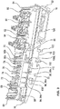
- the in Fig. 1 illustrated power distributor 2 comprises a feed module 4, six connection modules 6 and a signal module 8 as (power distribution) modules, wherein the connection module 6 in Fig. 2 is shown individually.
- Each module 4, 6, 8 comprises a separate, that is separated from the other modules 4, 6, 8 housing 10, 12 and 14.
- Each module 4, 6, 8 is formed like a DIN rail mounted device and accordingly has on a rear housing side 16th a groove-like receptacle 18, with which the respective module 4, 6, 8 can be snapped onto a mounting rail 20 for assembly purposes.
- the profile direction of this receptacle 18 - and correspondingly in the assembled state also the profile direction of the support rail 20 corresponding to this receptacle 18 - define a row direction 22 along which the modules 4, 6, 8 are lined up.
- two circuit breaker 24 are each arranged on a connection module 6 inside of the modules (4, 6, 8) formed (module) package, the feed module 4 on the one hand and the signal module 8 on the other hand, the connection modules 6 in the row direction 22 as side parts outside flank.
- each module 4, 6, 8 In the row direction 22 opposite housing surfaces of each module 4, 6, 8 are hereinafter referred to as (housing) end faces 26 of the respective module 4, 6, 8.
- the side of the housing opposite to the rear side 16 of each module 4, 6, 8 is designated as (housing) front side 28 of the module 4, 6, 8.
- This front side 28 is, when the power distributor 2 is mounted in a control cabinet, facing a user.
- the other two sides of the housing of each module 4, 6, 8 are - according to the conventional installation position of the module 4, 6, 8 - referred to as (housing) top 30 and (housing) bottom 32 regardless of the actual position in the surrounding space.
- the feed module 4 comprises a feed connection 34 for making electrical contact with a main circuit, not shown, and thus for supplying an electric current to the power distributor 2.
- the feed connection 34 is on the front side 28 of the housing 10 near the top side 30 arranged, and designed as a terminal for a wire or stranded conductor of the main circuit.
- the supply terminal 34 is electrically conductively coupled within the housing with a coupling contact, not shown, which is arranged within a groove-like housing slot 36.
- the feed module 4 has approximately halfway up the housing 10 a ground terminal 38 as a negative terminal (DC network) or as a neutral conductor (AC network).
- the mass connection 38 is electrically conductively coupled within the housing 10 with a lateral socket for a contact connection with the aligned connection module 6, as well as with a coupling contact which is positioned in a centered on the housing 10 housing slot 40 on the front side 28.
- the feed module 4 further comprises a return connection 42 for making electrical contact with a current return (not shown) in the course of a protective or functional earth.
- the return port 42 is disposed near the bottom 32 on the front side 28 of the housing 10, and as the feed port 34 and the mass port 38 is configured as a terminal.
- the return connection 42 is in turn electrically conductively coupled to a coupling contact within a housing slot 44 arranged in the region of the underside 32.
- the groove-like housing slots 36, 40, 44 are in particular so introduced into the housing 10 of the feed module 4 that they are open to the front side 28.
- the housing slots 36, 40, 42 extend in the row direction 22 substantially over the entire housing width and are thus open to the two opposite end faces 26 of the housing 10.
- connection terminals for a signal connection 46, for a data bus connection 48 and for an address bus connection 50 are provided on the front side of the housing.
- the terminals 46, 48, 50 are made smaller in size compared to the terminals 34, 38, 42, and preferably for the supply of low currents designed as switching or communication signals.
- the terminals 46, 48, 50 are similar to the ground terminal 38 within the housing 10, each coupled to a side socket for contacting with the connection module 6.
- the housing 14 of the signal module 8 has three housing slots 36, 40, 44, which are configured substantially identical to those of the feed module 4, but have no coupling contact with the housing interior. Between the lower housing slots 40 and 44, four terminals 52, 54, 56 and 58 are arranged as a ground terminal 52, a signal terminal 54, a data bus terminal 56 and an address bus terminal 58.
- the terminals 52, 54, 56, 58 are coupled within the housing 14 with contact elements for coupling contact with the connection module 6.
- the flat plug-like contact elements protrude at least partially out of the housing 14 from the end face 26 facing a connection module 6 in the assembled state.
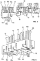
- connection module 6 Based on FIGS. 2 to 6 the structure of a connection module 6 is explained in more detail below, wherein exemplified in the Fig. 1 only one connection module 6 is provided with reference numerals.
- the housing 12 of the connection module 6 has three housing slots 36, 40 and 44, which are configured substantially identical to those of the feed module 4, each having a coupling contact 60, 62, 64 in the housing interior. Between the housing slots 36 and 40, a front-side slot 66 is mounted for the circuit breaker 24.
- the slot 66 has a first contact opening 68 for a (preferably designed as a flat plug) first plug contact of the circuit breaker 24 and a second contact opening 70 for a (preferably also designed as a flat plug) second plug contact of the circuit breaker 24th
- the slot 66 is also provided with five further contact openings 72, 74, 76, 78 and 80 for (preferably designed as a flat connector) corresponding signal or communication contacts of the circuit breaker.
- the contact openings 68, 70, 72, 74, 76, 78, 80 of the slot 66 are designed in particular as plug socket contacts.
- the contact openings or socket contacts 68, 70, 72, 74, 76, 78, 80 and the corresponding plug contacts of the circuit breaker 24 are designed to be complementary to each other in particular in the sense of male-female pairs.
- the slot 66 further has in the upper and lower regions each have a hook-like retaining element 82 for improved mounting of a populated circuit breaker 24.
- two terminals are arranged as load terminals 84 for connection of a load or load circuit, not shown.
- the load terminals 84 are internally coupled to the contact opening 70 electrically conductive by a conductor rail 86.
- the contact opening 68 in the interior of the housing 12 with the coupling contact 60 of the housing slot 36 is substantially integrally coupled by means of an electrically conductive conductor rail 88.
- connection module 6 further comprises four connection terminals 90, 92, which are arranged between the lower housing slots 40, 44 as two mass connections 92 and two return connections 90. Inside the housing 12, the mass terminals 92 are connected to a respective coupling contact 64 of the housing slot 44 and the return terminals 90 to each of a coupling contact 62 of the housing slot 40 electrically conductively connected.
- the socket contacts 70, 72, 74, 76, 78 are internally electrically coupled to four coupling contacts 94, 96, 98 and 100.
- the coupling contacts 94, 96, 98, 100 are designed in particular as plug-socket pairs, wherein the plug in the following the reference character suffix -a and the sockets have the reference character -b.
- the sockets 94b, 96b, 98b, 100b are arranged in frontal housing openings, wherein the plug 94a, 96a, 98a, 100a at least partially - as in particular in Fig. 3 seen - protrude from the opposite end face 26 of the housing 12.
- the housing 12 of the connection modules 6 have - as in Fig. 3 and Fig. 4 is clear - on the back 16 in the area of the receptacle 18, two locking tongues 102 on the respective end face 26 protrude laterally.
- the latching tongues 102 can be latched or clipped into place with corresponding latching receptacles 104 for the purpose of facilitating the assembly of the modules 4, 6, 8, wherein the latching receptacles 104 are expediently arranged on the opposite end side 26 to the latching tongues 102.
- the housings 12 further have on the latching tongue-side end face 26 two integrally formed and the end face 26 protruding joining extensions 106 for facilitated juxtaposition or juxtaposition of the modules 4, 6, 8. In the assembled state, the joining extensions 106 at least partially engage in corresponding joint receivers 108 of the adjacent modules 4, 6 for the purpose of a vibration-proof and reliable fastening.
- the plug-socket-like contact opening 80 is designed in particular as a two-part split socket contact.
- the plug base part contacts 80a, 80b formed thereby are coupled by means of a circuit board 110 arranged at the rear to the contact openings 68, 70, 72, 74, 76, 78.
- a base resistor 112 is connected to the board 110.
- the socket resistor 112 is connected in series between the coupling contacts 100a and 100b, and the board 110 is connected to the coupling contacts 98a, 98b.
- the modules 6, 8 by latching tongues 102 on the end faces 26 of each housing 12, 14 with corresponding locking receptacles 104 of the modules 4, 6 on the front side of each adjacent module 4, 6, 8 in alignment and detachable (plug) connected.
- the end faces 26 of the connection modules 6 are thus substantially completely covered by the feed module 4, adjacent connection modules 6 and the signal module 8.
- the housing slots 36, 40 and 44 of the adjacent modules 4, 6, 8 are aligned with each other, so that in each case a substantially continuous and rectilinear groove-like enforcement of the modules 4, 6, 8 is realized.
- the feed terminal 34 of the feed module 4 is connected in parallel with the juxtaposed modules 6 by a bus bar, not shown pressed into the aligned housing slots 36, and thus contacted with the corresponding coupling contacts 60.
- the busbar is dimensioned such that it extends over the total width of all modules 4, 6, 8 to be integrated into the power distributor 2.
- ground terminals 38, 52, 90 and the return terminals 42, 92 of the aligned modules 4, 6 are connected in parallel by pressing in each case a further bus bar in the housing slots 40 and 44, wherein the ground terminal 38 in particular with a negative conductor or neutral conductor and the return terminal 42 are connected in particular with a protective or functional earth as a feedback potential.
- the individual load circuits of the power distributor 2 are then connected to a respective associated connection module 6 by the respective supply lines of the load circuit to the load terminals 84 of the connection modules 6, and the return line of the load circuit to the terminals of the return terminals 90 of the connection modules 6 are electrically connected.
- each housing slot 36, 40, 44 of the modules 4, 8 in order to complete the housing slots 36, 40, 44 of the modules 4, 8 with respect to the front ends 26, which are respectively in the outer direction 22, in a touch-proof manner, each housing slot 36, 40, 44 - as in FIG Fig. 1 for the feed module 4 - provided on the outside with an insulating cover 114.
- an external controller 116 is provided as a control unit, which is connected to the data bus connection 48 and the address bus connection 50 to the feed module 4.
- the circuit breaker 24 each switch inside a controller 118 which is connected in the assembled state signaling to the controller 116.
- the interconnection of the controllers 116, 118 in the course of a bus functionality is schematic and simplified in FIG Fig. 7 shown.
- Fig. 7 shows a general power distributor 2 with N juxtaposed connection modules 6, wherein for simplicity, the feed module 4 and the signal module 8 of the power distributor 2 are not shown.
- the N connection modules 6 are each equipped in the illustrated embodiment with a circuit breaker 24 comprising the controller 118.
- the base resistors 112 of the aligned connection modules 6 are connected in series by the coupling contacts 100, and form a substantially continuous resistance chain 120 between the address bus terminals 50 and 58.
- the circuit breaker 24 is contacted with the plug-in base contact 80 with a two-part plug contact such that the controller 118 of the circuit breaker 24 is connected across the plug socket part contacts 80a, 80b substantially parallel to the socket resistor 112. Via the contact opening 76, the controller 118 is connected to a data bus line or communication line 122 formed by the coupling contacts 98.
- the plug socket part contact 80b is connected in the switch with the plug socket contact 72, the plug socket contact 72 being coupled in an electrically conductive manner via the coupling contacts 94, in particular to the ground terminal 38 of the feed module 4.
- a transistor 118 controlled by the controller 118 is connected as a switching element 124 in the circuit breaker 24. Is exemplary in the Fig. 7 only the N-th connection module 6 with the circuit breaker 24 provided with reference numerals.
- the controller 116 has a controller DC internal source 126 for energizing the resistor chain 120 with an addressing current I A. During operation, therefore, the addressing current I A flows through the resistor chain 120, so that a respective voltage U i drops across all the base resistors, the running index i being selected from 1 to N.
- the controller 116 is suitable and configured to determine the number N of the connected connection modules 6 on the basis of a number A. 116 To this end, detects the controller, an output voltage U 0 of the DC power source 126. In a known Adressierstrom I A and the known value of the electrical resistance of a single base resistor 112, the number value A obtained in a simple manner from the quotient of the output voltage U 0 and the voltage drop on a single socket resistor 112.
- Each controller 118 detects in operation on the socket part contact 80a the module-specific voltage value U i, where the voltage value of U i is always reduced with increasing length of the resistor string 120 between two connection modules 6 by a voltage drop at the respective base resistance 112th
- the controllers 118 send via the data bus 122 a controller signal C corresponding to the respective voltage U i to the controller 116.
- the controller 116 assigns a device address G i to each connected controller 118 on the basis of the received controller signals C.
- the respective device address G i results here, for example, in a simple manner from the integer rounded quotient of the respectively detected voltage U i and the voltage drop across a single base resistor 112.
- each circuit breaker 24 or each controller 118 a (physical) device address G. i , which decreases starting from the DC power source 126 along the resistor chain 120.
- the voltage U N is equal to the voltage drop across the base resistor 112, that is, the first device address G 1 is assigned to the Nth terminal module 6.
- the first connection module 6 of the resistor chain 120 receives the Nth device address G N , since the detected voltage U 1 is substantially equal to the output voltage U 0 of DC power source 126 is.
- the device address G N is sent by the controller 116 to the respective controller 118 and stored in an associated data memory of the controller 118.
- the controller 116 is adapted and configured for purposes of improved operability to implement the set of device addresses G i into a set of logical addresses L i corresponding to the order of the contiguous port modules 6.
- the logic addresses L i are substantially inverted in their order with respect to the device addresses, that is, the controller 118 of the first connection module 6 in the resistor chain 120 has the first logic address L 1 , the subsequent controller 118 has the second logic address L 2 etc. and the last controller 118 of the terminal module 6 arranged at the end of the resistor chain 120 has the Nth logic address L N. This makes the use of the power distributor 2 more intuitive for a user.
- the controller 116 is suitable for this purpose and is set up automatically to start a fault diagnosis in the event of a fault.
- an error case is understood to mean, in particular, a galvanic interruption 128 of the resistance chain 120, which in Fig. 7 merely exemplified between the third connection module 6 and the Nth connection module 6 is indicated.
- the current flow of the addressing current I A is interrupted by the resistor chain 120.
- the controller 116 then triggers a search process in a first method step 130.
- a power-on process 132 is first started.
- the controller 116 sends a switching signal S to all connected controllers 118 via the data bus 122.
- the respective controller 116 closes the respectively assigned switching element 124, so that the resistor chain 120 contacts the socket base contact in each case 80b and the socket contact 72 is connected to ground.
- an addressing current I A flows through the resistor chain 120 to ground.
- the number of connected connection modules 6 is detected by the controller 116 in a detection process 134 by determining the number A value.
- the device addresses G i are assigned by the controller 116 to the connected controllers 118 and sent.
- the respective device addresses G i are sent by the controllers 118 to the controller 116 as controller signals C, the controller 116 checking to see if the first device address G 1 is present.
- the controller 116 If a controller 116 is detected with the device address G 1 , the controller 116 starts a shutdown process 140 in which the controller 116 sends a switching signal S 'to the controller 118 with the device address G 1 .
- the controller 118 Upon receipt of the switching signal S ', the controller 118 turns off its associated switching element 124 so that the respective socket resistor 112 on the socket base contact 80b is no longer grounded. Thereby, the respective base resistor 112 is released from the composite of the resistor chain, and the addressing current I A flows through the series resistor 112 connected in series to ground. Subsequently, the respective controller 118 deletes, in an erase process 142, the first device address G 1 stored in the (data) memory of the controller 118, and a new detection process 132 of the controller 116 is started.
- the method steps of the search process from detection process 134, addressing process 136, query 138, switch-off process 140 and delete process 142 are repeated until controllers 118 do not report first device address G 1 to controller 116. Thereafter, the search is completed with an end process 144.
- the controller 116 reports in a result process 146 that the interruption 128 between the last detected controller 116 and the unrecognized port module 6 is located.
- the base resistors 112 for example, all have a resistance value of 1 k ⁇ , so that at a generated addressing current I A of preferably 1 mA at each base resistor 112, a voltage U i of 1 V drops.
Landscapes
- Engineering & Computer Science (AREA)
- Power Engineering (AREA)
- Physics & Mathematics (AREA)
- General Physics & Mathematics (AREA)
- Architecture (AREA)
- Automation & Control Theory (AREA)
- Civil Engineering (AREA)
- Structural Engineering (AREA)
- Distribution Board (AREA)
- Direct Current Feeding And Distribution (AREA)
- Emergency Protection Circuit Devices (AREA)
- Details Of Connecting Devices For Male And Female Coupling (AREA)
- Programmable Controllers (AREA)
- General Engineering & Computer Science (AREA)
Claims (8)
- Procédé de fonctionnement d'un coffret de distribution électrique (2) comprenant un premier contrôleur (116) et comprenant un certain nombre de modules de raccordement (6) juxtaposés ayant respectivement une résistance de socle (112) interne au module qui, avec les résistances de socle (112) des modules de raccordement (6) juxtaposés, forme une chaîne de résistances (120) branchées en série,- les modules de raccordement (6) étant respectivement équipés d'un disjoncteur (24) actionnable avec un deuxième contrôleur (118) interne au disjoncteur et avec un élément de commutation (124), lequel envoie au premier contrôleur (116) un signal de contrôleur (C) correspondant à la tension (Ui) qui chute aux bornes de la résistance de socle (112) respective,- une valeur de résistance totale de la chaîne de résistances (120) et, à l'aide de la valeur de résistance totale, une valeur de nombre (A) correspondant au certain nombre de modules de raccordement (6) accordés étant définies par le premier contrôleur (116),- une opération de recherche visant à déterminer la position de l'interruption (128) étant déclenchée dans le cas d'une interruption (128) galvanique de la chaîne de résistances (120),- au début de l'opération de recherche, tous les deuxièmes contrôleurs (118) raccordés étant placés dans un état de commutation avec lequel l'élément de commutation (124) respectif est fermé, et- la valeur de nombre (A) du nombre de modules de raccordement (6) raccordés étant définie pendant l'opération de recherche,- des adresses d'appareil (Gi) étant distribuées aux deuxièmes contrôleurs (118) raccordés, et- le deuxième contrôleur (118) ayant la première adresse d'appareil (G1) et l'élément de commutation (124) associé étant mis hors circuit.
- Procédé selon la revendication 1, des adresses d'appareil (Gi) spécifiques aux modules étant envoyées aux deuxièmes contrôleurs (118) raccordés en fonction des signaux de contrôleur (C) des deuxièmes contrôleurs (118) .
- Procédé selon la revendication 2, les adresses d'appareil (Gi) étant converties en un jeu d'adresses logiques (Li) correspondant à l'ordre des modules de raccordement (6) juxtaposés les uns aux autres en fonction de la valeur de nombre (A).
- Procédé selon la revendication 2 ou 3, l'opération de recherche prenant fin lorsqu'il n'existe aucun deuxième contrôleur (118) ayant la première adresse d'appareil (G1).
- Coffret de distribution électrique (2) comprenant un premier contrôleur (116) et comprenant un certain nombre de modules de raccordement (6) raccordés à celui-ci destinés au montage sur un rail porteur (20),- chaque module de raccordement (6) possédant un certain nombre de contacts de couplage latéraux (94, 96, 98, 100) servant à une liaison de contact électrique et/ou signalétique avec au moins un module de raccordement (6) supplémentaire juxtaposé ou juxtaposable au module de raccordement (6) respectif,- une résistance de socle (112) étant respectivement connectée en interne au module entre deux contacts de couplage (100a, 100b) de telle sorte que les résistances de socle (112) des modules de raccordement (6) juxtaposés les uns aux autres forment une chaîne de résistances (120) branchées en série,- les modules de raccordement (6) étant ou pouvant être respectivement équipés d'un disjoncteur (24) actionnable,- les disjoncteurs (24) possédant respectivement un deuxième contrôleur (118) interne au disjoncteur destiné à détecter une tension (Ui) qui chute aux bornes de la résistance de socle (112) respectivement associée et un élément de commutation (124) qui peut être actionné par le deuxième contrôleur (118), lequel est connecté ou peut être connecté entre la résistance de socle (112) et une borne de masse (72) du module de raccordement (6)- le deuxième contrôleur (118) envoyant un signal de contrôleur (C) au premier contrôleur (116) en fonction de la tension (Ui) détectée,- le premier contrôleur (116) possédant une source de courant continu (126) servant à l'alimentation de la chaîne de résistances (120), et- le premier contrôleur (116) et le deuxième contrôleur (118) étant conçu, du point de vue de la technique de programme et/ou de circuit, pour mettre en oeuvre le procédé selon l'une des revendications 1 à 4.
- Coffret de distribution électrique (2) selon la revendication 5, une ligne de communication (122) formée par les contacts de couplage (98a, 98b) étant présente pour le cheminement des signaux de contrôleur (C) .
- Coffret de distribution électrique (2) selon la revendication 5 ou 6,- le module de raccordement (6) possédant une ouverture de contact (80) qui comprend un contact de socle à enfichage divisé en deux pour un contact à enfichage du disjoncteur (24), et- la résistance de socle (112) étant connectée entre les contacts partiels de socle à enfichage (80a, 80b) ainsi formés.
- Coffret de distribution électrique (2) selon la revendication 7,- la borne de masse (72) étant mise en contact ou pouvant être mise en contact d'un côté avec le deuxième contrôleur (118) respectif et de l'autre côté avec un contact partiel à enfichage du contact à enfichage, et- l'élément de commutation (124) étant connecté entre la borne de masse (72) et le contact partiel à enfichage.
Applications Claiming Priority (2)
| Application Number | Priority Date | Filing Date | Title |
|---|---|---|---|
| DE102015221899.6A DE102015221899B3 (de) | 2015-11-06 | 2015-11-06 | Stromverteiler |
| PCT/EP2016/068462 WO2017076526A1 (fr) | 2015-11-06 | 2016-08-02 | Distributeur de courant |
Publications (2)
| Publication Number | Publication Date |
|---|---|
| EP3338149A1 EP3338149A1 (fr) | 2018-06-27 |
| EP3338149B1 true EP3338149B1 (fr) | 2019-10-09 |
Family
ID=56694111
Family Applications (1)
| Application Number | Title | Priority Date | Filing Date |
|---|---|---|---|
| EP16753294.4A Active EP3338149B1 (fr) | 2015-11-06 | 2016-08-02 | Méthode d'exploitation d'un distributeur de courant et distributeur de courant |
Country Status (8)
| Country | Link |
|---|---|
| US (1) | US10707654B2 (fr) |
| EP (1) | EP3338149B1 (fr) |
| JP (1) | JP6728347B2 (fr) |
| CN (1) | CN108351628B (fr) |
| CA (1) | CA3002412C (fr) |
| DE (2) | DE102015221899B3 (fr) |
| ES (1) | ES2757956T3 (fr) |
| WO (1) | WO2017076526A1 (fr) |
Families Citing this family (12)
| Publication number | Priority date | Publication date | Assignee | Title |
|---|---|---|---|---|
| DE102019203521A1 (de) * | 2019-03-15 | 2020-09-17 | Ellenberger & Poensgen Gmbh | Verfahren zum Betrieb eines Stromverteilers |
| CN112838668B (zh) * | 2019-11-22 | 2024-05-17 | 华为数字能源技术有限公司 | 一种断路器识别方法、装置和设备 |
| CN112952564B (zh) * | 2019-12-25 | 2022-04-22 | 华为数字能源技术有限公司 | 配电模块及通信电源系统 |
| DE102020106648A1 (de) | 2020-03-11 | 2021-09-16 | Phoenix Contact Gmbh & Co. Kg | Technik zur Energieversorgung und Kommunikation in einem Leistungsschutzsystem |
| DE102020203560A1 (de) * | 2020-03-19 | 2021-09-23 | Ellenberger & Poensgen Gmbh | Stromverteiler eines Bordnetzes eines Kraftfahrzeugs |
| CN111830868A (zh) * | 2020-07-01 | 2020-10-27 | 孙安萍 | 一种功能模块、通信方法及应用该模块的量热仪 |
| DE102020128847B3 (de) * | 2020-11-03 | 2022-06-02 | Bender Gmbh & Co. Kg | Tragschienen-Busanordnung mit separaten Detektionsleiterbahnen und automatischer Busadressierung |
| EP4378285A1 (fr) * | 2021-07-27 | 2024-06-05 | Honeywell International Inc. | Base de remplacement à chaud pour un dispositif de commande de bâtiment |
| CN114429888B (zh) * | 2021-12-20 | 2023-12-12 | 杭州鸿雁电力电气有限公司 | 一种便于模块化装配物联网断路器的配电系统 |
| CN116155866B (zh) * | 2023-04-20 | 2023-06-20 | 中大智能科技股份有限公司 | 基于电流检测的阵列式位移计的地址自动分配方法和排序方法 |
| DE102023120295B4 (de) * | 2023-07-31 | 2025-06-05 | Eugen Forschner Gmbh | Stromverteiler und Kraftfahrzeug mit einem solchen Stromverteiler |
| DE102024101910A1 (de) * | 2024-01-23 | 2025-07-24 | Warema Renkhoff Se | Steuergerät für Gebäudeautomation |
Family Cites Families (19)
| Publication number | Priority date | Publication date | Assignee | Title |
|---|---|---|---|---|
| US5831546A (en) * | 1996-05-10 | 1998-11-03 | General Signal Corporation | Automatic addressing in life safety system |
| DE19964156B4 (de) * | 1999-01-25 | 2004-07-15 | Weidmüller Interface Gmbh & Co. | Elektrisches Gerät |
| DE202004008141U1 (de) * | 2004-05-24 | 2005-10-06 | Ellenberger & Poensgen Gmbh | Modularer Stromverteiler für hohe Ströme |
| FR2875071B1 (fr) * | 2004-09-03 | 2006-11-24 | Inst Nat Rech Inf Automat | Dispositif de repartition de courant entre des cathodes d'une electrode multipolaire, notamment d'un implant |
| DE102007013712A1 (de) * | 2007-03-22 | 2008-09-25 | Ellenberger & Poensgen Gmbh | Verfahren und Vorrichtung zur Auswertung schneller Stromänderungen |
| US20090021879A1 (en) * | 2007-07-17 | 2009-01-22 | Rivers Jr Cecil | Apparatus and method for fault current interruption |
| JP2009188371A (ja) * | 2008-01-11 | 2009-08-20 | Panasonic Corp | 半導体装置及びその評価方法 |
| EP2154831A1 (fr) * | 2008-08-11 | 2010-02-17 | Siemens Aktiengesellschaft | Procédé de détermination de l'adresse ou de la position d'un abonné |
| DE102010016865A1 (de) * | 2010-05-10 | 2011-11-10 | Weidmüller Interface GmbH & Co. KG | Tragschienenbussystem |
| US8961201B2 (en) * | 2010-05-10 | 2015-02-24 | Weidmueller Interface Gmbh & Co. Kg | Mounting rail bus system |
| DE102012110172B4 (de) * | 2012-10-24 | 2017-11-16 | Phoenix Contact Gmbh & Co. Kg | Bussystem mit Wechselspannungsversorgung |
| US8986030B2 (en) * | 2012-12-06 | 2015-03-24 | Phoenix Contact Development and Manufacturing, Inc. | Modular electric power distribution system |
| US20140233160A1 (en) * | 2013-02-19 | 2014-08-21 | Eaton Corporation | Load Centers Including Position Sensing Circuits and Related Systems and Sensing Circuits |
| PL2863496T3 (pl) * | 2013-10-18 | 2018-02-28 | Wöhner GmbH & Co. KG Elektrotechnische Systeme | System ochrony przed dotykiem do prądowych szyn zbiorczych |
| JP6136015B2 (ja) * | 2013-10-30 | 2017-05-31 | パナソニックIpマネジメント株式会社 | 分電盤システム、エネルギ管理システム、分電盤、配線用遮断器、およびアダプタ |
| DE102013018282A1 (de) * | 2013-10-31 | 2015-05-21 | Nxtcontrol Gmbh | Verfahren zur Identifizierung der relativen Einbauposition der in einem modularen elektronischen System zur Verwendung kommenden Module |
| US9876334B2 (en) | 2014-01-03 | 2018-01-23 | Electronic Theatre Controls, Inc. | Breaker assembly with mating platform and well connection |
| DE202014009245U1 (de) * | 2014-11-21 | 2016-02-24 | Ellenberger & Poensgen Gmbh | Schaltgerät sowie Schaltgeräteanordnung |
| DE102015213744A1 (de) * | 2015-07-21 | 2017-01-26 | Ellenberger & Poensgen Gmbh | Stromverteiler |
-
2015
- 2015-11-06 DE DE102015221899.6A patent/DE102015221899B3/de not_active Expired - Fee Related
- 2015-11-06 DE DE202015009241.1U patent/DE202015009241U1/de not_active Expired - Lifetime
-
2016
- 2016-08-02 CN CN201680060024.3A patent/CN108351628B/zh active Active
- 2016-08-02 EP EP16753294.4A patent/EP3338149B1/fr active Active
- 2016-08-02 JP JP2018519919A patent/JP6728347B2/ja active Active
- 2016-08-02 CA CA3002412A patent/CA3002412C/fr active Active
- 2016-08-02 WO PCT/EP2016/068462 patent/WO2017076526A1/fr not_active Ceased
- 2016-08-02 ES ES16753294T patent/ES2757956T3/es active Active
-
2018
- 2018-05-07 US US15/972,751 patent/US10707654B2/en active Active
Non-Patent Citations (1)
| Title |
|---|
| None * |
Also Published As
| Publication number | Publication date |
|---|---|
| CA3002412C (fr) | 2023-03-14 |
| WO2017076526A1 (fr) | 2017-05-11 |
| JP2018533900A (ja) | 2018-11-15 |
| EP3338149A1 (fr) | 2018-06-27 |
| US20180254615A1 (en) | 2018-09-06 |
| DE202015009241U1 (de) | 2016-12-27 |
| CN108351628B (zh) | 2020-12-22 |
| US10707654B2 (en) | 2020-07-07 |
| CN108351628A (zh) | 2018-07-31 |
| ES2757956T3 (es) | 2020-04-30 |
| DE102015221899B3 (de) | 2016-12-22 |
| JP6728347B2 (ja) | 2020-07-22 |
| CA3002412A1 (fr) | 2017-05-11 |
Similar Documents
| Publication | Publication Date | Title |
|---|---|---|
| EP3338149B1 (fr) | Méthode d'exploitation d'un distributeur de courant et distributeur de courant | |
| DE102016111690B4 (de) | Stromverteiler für ein Fahrzeug | |
| DE69331927T2 (de) | Rechnergesteuerte schalteranordnung mit identifikationsschaltung | |
| EP3447785B1 (fr) | Distributeur de courant | |
| DE3713262A1 (de) | Steckverbindungs-codierung fuer elektrische kabel | |
| DE102005040348B4 (de) | Verbindungssystem mit einem elektromagnetischem Schaltgerät, insbesondere Schütz, und einem Stecker | |
| DE102007027522B3 (de) | Schaltgerät | |
| DE202014009245U1 (de) | Schaltgerät sowie Schaltgeräteanordnung | |
| WO2018215547A1 (fr) | Tableau de distribution électrique | |
| EP3925039A1 (fr) | Procédé pour faire fonctionner un distributeur de courant | |
| DE102005025108B3 (de) | Vorrichtung zum Testen einer Schutz-, Mess- oder Zähleinrichtung als Bestandteil einer Mittel- oder Hochspannungsanlage, insbesondere eines Netzschutzrelais, einer Generatorschutzeinrichtung, eines Stromzählers ect. in einer Mittel- oder Hochspannungsanlage | |
| EP4078738B1 (fr) | Technique pour éviter un arc électrique lors de la séparation d'une connexion de courant continu au moyen d'une rallonge d'une interconnexion de lignes | |
| DE102015215783A1 (de) | Verfahren und Vorrichtung zum Konfigurieren einer Steuervorrichtung in einem Kraftfahrzeug | |
| EP0821458B1 (fr) | Dispositif de répartition de lignes | |
| DE3879641T2 (de) | Statischer Auslöser mit externer Versorgung. | |
| DE10052846C2 (de) | Anordnung zur Verzweigung elektrischer Stromkreise im explosionsgefährdeten Bereich | |
| DE10242921B4 (de) | Ethernet-Stecker, Ethernet-Endgerät sowie Ethernet-Kommunikationssystem | |
| DE202012002395U1 (de) | Elektrischer Steckverbinder | |
| EP2140470B1 (fr) | Module avec extension automatique d'un circuit de controle | |
| EP2551969B1 (fr) | Boîte de jonction pour conduites électriques et système de répartition électrique avec des boîtes de jonction de ce type | |
| WO2007137535A1 (fr) | Dispositif de contrôle d'une armoire électrique dotée d'un bornier d'entrée | |
| DE102018204180B4 (de) | Elektrische Schaltvorrichtung sowie Verfahren zur Herstellung einer elektrischen Schaltvorrichtung | |
| DE102006000977B3 (de) | Adapter zum Anschluss eines signaltechnisch antivalent detektierenden Sensor | |
| DE19716819C2 (de) | Prüfgerät für spannungsführende Leiter in Schaltanlagen, insbesondere Dauer-Spannungsanzeiger | |
| DE3718872A1 (de) | Elektrische steckverbindung, insbesondere fuer heizanlagen |
Legal Events
| Date | Code | Title | Description |
|---|---|---|---|
| STAA | Information on the status of an ep patent application or granted ep patent |
Free format text: STATUS: THE INTERNATIONAL PUBLICATION HAS BEEN MADE |
|
| PUAI | Public reference made under article 153(3) epc to a published international application that has entered the european phase |
Free format text: ORIGINAL CODE: 0009012 |
|
| STAA | Information on the status of an ep patent application or granted ep patent |
Free format text: STATUS: REQUEST FOR EXAMINATION WAS MADE |
|
| 17P | Request for examination filed |
Effective date: 20180227 |
|
| AK | Designated contracting states |
Kind code of ref document: A1 Designated state(s): AL AT BE BG CH CY CZ DE DK EE ES FI FR GB GR HR HU IE IS IT LI LT LU LV MC MK MT NL NO PL PT RO RS SE SI SK SM TR |
|
| AX | Request for extension of the european patent |
Extension state: BA ME |
|
| REG | Reference to a national code |
Ref country code: DE Ref legal event code: R079 Ref document number: 502016007031 Country of ref document: DE Free format text: PREVIOUS MAIN CLASS: G05B0019042000 Ipc: H02J0013000000 |
|
| GRAP | Despatch of communication of intention to grant a patent |
Free format text: ORIGINAL CODE: EPIDOSNIGR1 |
|
| STAA | Information on the status of an ep patent application or granted ep patent |
Free format text: STATUS: GRANT OF PATENT IS INTENDED |
|
| RIC1 | Information provided on ipc code assigned before grant |
Ipc: H02B 1/056 20060101ALI20181219BHEP Ipc: H02B 1/20 20060101ALI20181219BHEP Ipc: H02J 13/00 20060101AFI20181219BHEP |
|
| DAV | Request for validation of the european patent (deleted) | ||
| DAX | Request for extension of the european patent (deleted) | ||
| INTG | Intention to grant announced |
Effective date: 20190114 |
|
| GRAJ | Information related to disapproval of communication of intention to grant by the applicant or resumption of examination proceedings by the epo deleted |
Free format text: ORIGINAL CODE: EPIDOSDIGR1 |
|
| STAA | Information on the status of an ep patent application or granted ep patent |
Free format text: STATUS: REQUEST FOR EXAMINATION WAS MADE |
|
| GRAP | Despatch of communication of intention to grant a patent |
Free format text: ORIGINAL CODE: EPIDOSNIGR1 |
|
| STAA | Information on the status of an ep patent application or granted ep patent |
Free format text: STATUS: GRANT OF PATENT IS INTENDED |
|
| INTC | Intention to grant announced (deleted) | ||
| INTG | Intention to grant announced |
Effective date: 20190520 |
|
| GRAS | Grant fee paid |
Free format text: ORIGINAL CODE: EPIDOSNIGR3 |
|
| GRAA | (expected) grant |
Free format text: ORIGINAL CODE: 0009210 |
|
| STAA | Information on the status of an ep patent application or granted ep patent |
Free format text: STATUS: THE PATENT HAS BEEN GRANTED |
|
| AK | Designated contracting states |
Kind code of ref document: B1 Designated state(s): AL AT BE BG CH CY CZ DE DK EE ES FI FR GB GR HR HU IE IS IT LI LT LU LV MC MK MT NL NO PL PT RO RS SE SI SK SM TR |
|
| REG | Reference to a national code |
Ref country code: GB Ref legal event code: FG4D Free format text: NOT ENGLISH |
|
| REG | Reference to a national code |
Ref country code: CH Ref legal event code: EP |
|
| REG | Reference to a national code |
Ref country code: DE Ref legal event code: R096 Ref document number: 502016007031 Country of ref document: DE |
|
| REG | Reference to a national code |
Ref country code: IE Ref legal event code: FG4D Free format text: LANGUAGE OF EP DOCUMENT: GERMAN |
|
| REG | Reference to a national code |
Ref country code: CH Ref legal event code: NV Representative=s name: E. BLUM AND CO. AG PATENT- UND MARKENANWAELTE , CH |
|
| REG | Reference to a national code |
Ref country code: AT Ref legal event code: REF Ref document number: 1189954 Country of ref document: AT Kind code of ref document: T Effective date: 20191115 |
|
| REG | Reference to a national code |
Ref country code: SE Ref legal event code: TRGR |
|
| REG | Reference to a national code |
Ref country code: NL Ref legal event code: FP |
|
| REG | Reference to a national code |
Ref country code: LT Ref legal event code: MG4D |
|
| REG | Reference to a national code |
Ref country code: ES Ref legal event code: FG2A Ref document number: 2757956 Country of ref document: ES Kind code of ref document: T3 Effective date: 20200430 |
|
| PG25 | Lapsed in a contracting state [announced via postgrant information from national office to epo] |
Ref country code: PL Free format text: LAPSE BECAUSE OF FAILURE TO SUBMIT A TRANSLATION OF THE DESCRIPTION OR TO PAY THE FEE WITHIN THE PRESCRIBED TIME-LIMIT Effective date: 20191009 Ref country code: LT Free format text: LAPSE BECAUSE OF FAILURE TO SUBMIT A TRANSLATION OF THE DESCRIPTION OR TO PAY THE FEE WITHIN THE PRESCRIBED TIME-LIMIT Effective date: 20191009 Ref country code: NO Free format text: LAPSE BECAUSE OF FAILURE TO SUBMIT A TRANSLATION OF THE DESCRIPTION OR TO PAY THE FEE WITHIN THE PRESCRIBED TIME-LIMIT Effective date: 20200109 Ref country code: PT Free format text: LAPSE BECAUSE OF FAILURE TO SUBMIT A TRANSLATION OF THE DESCRIPTION OR TO PAY THE FEE WITHIN THE PRESCRIBED TIME-LIMIT Effective date: 20200210 Ref country code: LV Free format text: LAPSE BECAUSE OF FAILURE TO SUBMIT A TRANSLATION OF THE DESCRIPTION OR TO PAY THE FEE WITHIN THE PRESCRIBED TIME-LIMIT Effective date: 20191009 Ref country code: GR Free format text: LAPSE BECAUSE OF FAILURE TO SUBMIT A TRANSLATION OF THE DESCRIPTION OR TO PAY THE FEE WITHIN THE PRESCRIBED TIME-LIMIT Effective date: 20200110 Ref country code: BG Free format text: LAPSE BECAUSE OF FAILURE TO SUBMIT A TRANSLATION OF THE DESCRIPTION OR TO PAY THE FEE WITHIN THE PRESCRIBED TIME-LIMIT Effective date: 20200109 Ref country code: FI Free format text: LAPSE BECAUSE OF FAILURE TO SUBMIT A TRANSLATION OF THE DESCRIPTION OR TO PAY THE FEE WITHIN THE PRESCRIBED TIME-LIMIT Effective date: 20191009 |
|
| PG25 | Lapsed in a contracting state [announced via postgrant information from national office to epo] |
Ref country code: RS Free format text: LAPSE BECAUSE OF FAILURE TO SUBMIT A TRANSLATION OF THE DESCRIPTION OR TO PAY THE FEE WITHIN THE PRESCRIBED TIME-LIMIT Effective date: 20191009 Ref country code: HR Free format text: LAPSE BECAUSE OF FAILURE TO SUBMIT A TRANSLATION OF THE DESCRIPTION OR TO PAY THE FEE WITHIN THE PRESCRIBED TIME-LIMIT Effective date: 20191009 Ref country code: IS Free format text: LAPSE BECAUSE OF FAILURE TO SUBMIT A TRANSLATION OF THE DESCRIPTION OR TO PAY THE FEE WITHIN THE PRESCRIBED TIME-LIMIT Effective date: 20200224 |
|
| PG25 | Lapsed in a contracting state [announced via postgrant information from national office to epo] |
Ref country code: AL Free format text: LAPSE BECAUSE OF FAILURE TO SUBMIT A TRANSLATION OF THE DESCRIPTION OR TO PAY THE FEE WITHIN THE PRESCRIBED TIME-LIMIT Effective date: 20191009 |
|
| REG | Reference to a national code |
Ref country code: DE Ref legal event code: R097 Ref document number: 502016007031 Country of ref document: DE |
|
| PG2D | Information on lapse in contracting state deleted |
Ref country code: IS |
|
| PG25 | Lapsed in a contracting state [announced via postgrant information from national office to epo] |
Ref country code: IS Free format text: LAPSE BECAUSE OF FAILURE TO SUBMIT A TRANSLATION OF THE DESCRIPTION OR TO PAY THE FEE WITHIN THE PRESCRIBED TIME-LIMIT Effective date: 20200209 Ref country code: RO Free format text: LAPSE BECAUSE OF FAILURE TO SUBMIT A TRANSLATION OF THE DESCRIPTION OR TO PAY THE FEE WITHIN THE PRESCRIBED TIME-LIMIT Effective date: 20191009 Ref country code: CZ Free format text: LAPSE BECAUSE OF FAILURE TO SUBMIT A TRANSLATION OF THE DESCRIPTION OR TO PAY THE FEE WITHIN THE PRESCRIBED TIME-LIMIT Effective date: 20191009 Ref country code: EE Free format text: LAPSE BECAUSE OF FAILURE TO SUBMIT A TRANSLATION OF THE DESCRIPTION OR TO PAY THE FEE WITHIN THE PRESCRIBED TIME-LIMIT Effective date: 20191009 Ref country code: DK Free format text: LAPSE BECAUSE OF FAILURE TO SUBMIT A TRANSLATION OF THE DESCRIPTION OR TO PAY THE FEE WITHIN THE PRESCRIBED TIME-LIMIT Effective date: 20191009 |
|
| PLBE | No opposition filed within time limit |
Free format text: ORIGINAL CODE: 0009261 |
|
| STAA | Information on the status of an ep patent application or granted ep patent |
Free format text: STATUS: NO OPPOSITION FILED WITHIN TIME LIMIT |
|
| PG25 | Lapsed in a contracting state [announced via postgrant information from national office to epo] |
Ref country code: SM Free format text: LAPSE BECAUSE OF FAILURE TO SUBMIT A TRANSLATION OF THE DESCRIPTION OR TO PAY THE FEE WITHIN THE PRESCRIBED TIME-LIMIT Effective date: 20191009 Ref country code: SK Free format text: LAPSE BECAUSE OF FAILURE TO SUBMIT A TRANSLATION OF THE DESCRIPTION OR TO PAY THE FEE WITHIN THE PRESCRIBED TIME-LIMIT Effective date: 20191009 |
|
| 26N | No opposition filed |
Effective date: 20200710 |
|
| PG25 | Lapsed in a contracting state [announced via postgrant information from national office to epo] |
Ref country code: SI Free format text: LAPSE BECAUSE OF FAILURE TO SUBMIT A TRANSLATION OF THE DESCRIPTION OR TO PAY THE FEE WITHIN THE PRESCRIBED TIME-LIMIT Effective date: 20191009 |
|
| PG25 | Lapsed in a contracting state [announced via postgrant information from national office to epo] |
Ref country code: MC Free format text: LAPSE BECAUSE OF FAILURE TO SUBMIT A TRANSLATION OF THE DESCRIPTION OR TO PAY THE FEE WITHIN THE PRESCRIBED TIME-LIMIT Effective date: 20191009 |
|
| PG25 | Lapsed in a contracting state [announced via postgrant information from national office to epo] |
Ref country code: LU Free format text: LAPSE BECAUSE OF NON-PAYMENT OF DUE FEES Effective date: 20200802 |
|
| PG25 | Lapsed in a contracting state [announced via postgrant information from national office to epo] |
Ref country code: IE Free format text: LAPSE BECAUSE OF NON-PAYMENT OF DUE FEES Effective date: 20200802 |
|
| PG25 | Lapsed in a contracting state [announced via postgrant information from national office to epo] |
Ref country code: TR Free format text: LAPSE BECAUSE OF FAILURE TO SUBMIT A TRANSLATION OF THE DESCRIPTION OR TO PAY THE FEE WITHIN THE PRESCRIBED TIME-LIMIT Effective date: 20191009 Ref country code: MT Free format text: LAPSE BECAUSE OF FAILURE TO SUBMIT A TRANSLATION OF THE DESCRIPTION OR TO PAY THE FEE WITHIN THE PRESCRIBED TIME-LIMIT Effective date: 20191009 Ref country code: CY Free format text: LAPSE BECAUSE OF FAILURE TO SUBMIT A TRANSLATION OF THE DESCRIPTION OR TO PAY THE FEE WITHIN THE PRESCRIBED TIME-LIMIT Effective date: 20191009 |
|
| PG25 | Lapsed in a contracting state [announced via postgrant information from national office to epo] |
Ref country code: MK Free format text: LAPSE BECAUSE OF FAILURE TO SUBMIT A TRANSLATION OF THE DESCRIPTION OR TO PAY THE FEE WITHIN THE PRESCRIBED TIME-LIMIT Effective date: 20191009 |
|
| P01 | Opt-out of the competence of the unified patent court (upc) registered |
Effective date: 20231120 |
|
| PGFP | Annual fee paid to national office [announced via postgrant information from national office to epo] |
Ref country code: NL Payment date: 20250821 Year of fee payment: 10 |
|
| PGFP | Annual fee paid to national office [announced via postgrant information from national office to epo] |
Ref country code: ES Payment date: 20250917 Year of fee payment: 10 |
|
| PGFP | Annual fee paid to national office [announced via postgrant information from national office to epo] |
Ref country code: DE Payment date: 20250827 Year of fee payment: 10 |
|
| PGFP | Annual fee paid to national office [announced via postgrant information from national office to epo] |
Ref country code: IT Payment date: 20250829 Year of fee payment: 10 |
|
| PGFP | Annual fee paid to national office [announced via postgrant information from national office to epo] |
Ref country code: GB Payment date: 20250818 Year of fee payment: 10 Ref country code: BE Payment date: 20250820 Year of fee payment: 10 |
|
| PGFP | Annual fee paid to national office [announced via postgrant information from national office to epo] |
Ref country code: FR Payment date: 20250821 Year of fee payment: 10 Ref country code: AT Payment date: 20250819 Year of fee payment: 10 |
|
| PGFP | Annual fee paid to national office [announced via postgrant information from national office to epo] |
Ref country code: CH Payment date: 20250901 Year of fee payment: 10 Ref country code: SE Payment date: 20250821 Year of fee payment: 10 |