EP3339821B1 - Bildsensor - Google Patents
Bildsensor Download PDFInfo
- Publication number
- EP3339821B1 EP3339821B1 EP17205057.7A EP17205057A EP3339821B1 EP 3339821 B1 EP3339821 B1 EP 3339821B1 EP 17205057 A EP17205057 A EP 17205057A EP 3339821 B1 EP3339821 B1 EP 3339821B1
- Authority
- EP
- European Patent Office
- Prior art keywords
- light
- detecting elements
- array
- imaging sensor
- detecting element
- Prior art date
- Legal status (The legal status is an assumption and is not a legal conclusion. Google has not performed a legal analysis and makes no representation as to the accuracy of the status listed.)
- Active
Links
Images


Classifications
-
- H—ELECTRICITY
- H10—SEMICONDUCTOR DEVICES; ELECTRIC SOLID-STATE DEVICES NOT OTHERWISE PROVIDED FOR
- H10F—INORGANIC SEMICONDUCTOR DEVICES SENSITIVE TO INFRARED RADIATION, LIGHT, ELECTROMAGNETIC RADIATION OF SHORTER WAVELENGTH OR CORPUSCULAR RADIATION
- H10F39/00—Integrated devices, or assemblies of multiple devices, comprising at least one element covered by group H10F30/00, e.g. radiation detectors comprising photodiode arrays
- H10F39/80—Constructional details of image sensors
- H10F39/805—Coatings
- H10F39/8057—Optical shielding
-
- G—PHYSICS
- G01—MEASURING; TESTING
- G01J—MEASUREMENT OF INTENSITY, VELOCITY, SPECTRAL CONTENT, POLARISATION, PHASE OR PULSE CHARACTERISTICS OF INFRARED, VISIBLE OR ULTRAVIOLET LIGHT; COLORIMETRY; RADIATION PYROMETRY
- G01J1/00—Photometry, e.g. photographic exposure meter
- G01J1/42—Photometry, e.g. photographic exposure meter using electric radiation detectors
- G01J1/4228—Photometry, e.g. photographic exposure meter using electric radiation detectors arrangements with two or more detectors, e.g. for sensitivity compensation
-
- G—PHYSICS
- G01—MEASURING; TESTING
- G01J—MEASUREMENT OF INTENSITY, VELOCITY, SPECTRAL CONTENT, POLARISATION, PHASE OR PULSE CHARACTERISTICS OF INFRARED, VISIBLE OR ULTRAVIOLET LIGHT; COLORIMETRY; RADIATION PYROMETRY
- G01J3/00—Spectrometry; Spectrophotometry; Monochromators; Measuring colours
- G01J3/02—Details
- G01J3/0205—Optical elements not provided otherwise, e.g. optical manifolds, diffusers, windows
- G01J3/0229—Optical elements not provided otherwise, e.g. optical manifolds, diffusers, windows using masks, aperture plates, spatial light modulators or spatial filters, e.g. reflective filters
-
- G—PHYSICS
- G01—MEASURING; TESTING
- G01J—MEASUREMENT OF INTENSITY, VELOCITY, SPECTRAL CONTENT, POLARISATION, PHASE OR PULSE CHARACTERISTICS OF INFRARED, VISIBLE OR ULTRAVIOLET LIGHT; COLORIMETRY; RADIATION PYROMETRY
- G01J3/00—Spectrometry; Spectrophotometry; Monochromators; Measuring colours
- G01J3/12—Generating the spectrum; Monochromators
- G01J3/26—Generating the spectrum; Monochromators using multiple reflection, e.g. Fabry-Perot interferometer, variable interference filters
-
- G—PHYSICS
- G01—MEASURING; TESTING
- G01J—MEASUREMENT OF INTENSITY, VELOCITY, SPECTRAL CONTENT, POLARISATION, PHASE OR PULSE CHARACTERISTICS OF INFRARED, VISIBLE OR ULTRAVIOLET LIGHT; COLORIMETRY; RADIATION PYROMETRY
- G01J3/00—Spectrometry; Spectrophotometry; Monochromators; Measuring colours
- G01J3/28—Investigating the spectrum
- G01J3/2803—Investigating the spectrum using photoelectric array detector
-
- H—ELECTRICITY
- H10—SEMICONDUCTOR DEVICES; ELECTRIC SOLID-STATE DEVICES NOT OTHERWISE PROVIDED FOR
- H10F—INORGANIC SEMICONDUCTOR DEVICES SENSITIVE TO INFRARED RADIATION, LIGHT, ELECTROMAGNETIC RADIATION OF SHORTER WAVELENGTH OR CORPUSCULAR RADIATION
- H10F39/00—Integrated devices, or assemblies of multiple devices, comprising at least one element covered by group H10F30/00, e.g. radiation detectors comprising photodiode arrays
- H10F39/10—Integrated devices
- H10F39/12—Image sensors
- H10F39/18—Complementary metal-oxide-semiconductor [CMOS] image sensors; Photodiode array image sensors
-
- H—ELECTRICITY
- H10—SEMICONDUCTOR DEVICES; ELECTRIC SOLID-STATE DEVICES NOT OTHERWISE PROVIDED FOR
- H10F—INORGANIC SEMICONDUCTOR DEVICES SENSITIVE TO INFRARED RADIATION, LIGHT, ELECTROMAGNETIC RADIATION OF SHORTER WAVELENGTH OR CORPUSCULAR RADIATION
- H10F39/00—Integrated devices, or assemblies of multiple devices, comprising at least one element covered by group H10F30/00, e.g. radiation detectors comprising photodiode arrays
- H10F39/10—Integrated devices
- H10F39/12—Image sensors
- H10F39/199—Back-illuminated image sensors
-
- H—ELECTRICITY
- H10—SEMICONDUCTOR DEVICES; ELECTRIC SOLID-STATE DEVICES NOT OTHERWISE PROVIDED FOR
- H10F—INORGANIC SEMICONDUCTOR DEVICES SENSITIVE TO INFRARED RADIATION, LIGHT, ELECTROMAGNETIC RADIATION OF SHORTER WAVELENGTH OR CORPUSCULAR RADIATION
- H10F39/00—Integrated devices, or assemblies of multiple devices, comprising at least one element covered by group H10F30/00, e.g. radiation detectors comprising photodiode arrays
- H10F39/80—Constructional details of image sensors
- H10F39/802—Geometry or disposition of elements in pixels, e.g. address-lines or gate electrodes
- H10F39/8027—Geometry of the photosensitive area
-
- H—ELECTRICITY
- H10—SEMICONDUCTOR DEVICES; ELECTRIC SOLID-STATE DEVICES NOT OTHERWISE PROVIDED FOR
- H10F—INORGANIC SEMICONDUCTOR DEVICES SENSITIVE TO INFRARED RADIATION, LIGHT, ELECTROMAGNETIC RADIATION OF SHORTER WAVELENGTH OR CORPUSCULAR RADIATION
- H10F39/00—Integrated devices, or assemblies of multiple devices, comprising at least one element covered by group H10F30/00, e.g. radiation detectors comprising photodiode arrays
- H10F39/80—Constructional details of image sensors
- H10F39/805—Coatings
- H10F39/8053—Colour filters
Definitions
- the present invention relates to an imaging sensor.
- the present invention also relates to a system including the imaging sensor and to the use of the imaging sensor.
- the present invention relates to an imaging sensor arranged to provide an even signal from the light-detecting elements of the imaging sensor.
- Spectral imaging implies that spectral content of an image of an object is extracted and incident light on an imaging sensor relating to multiple ranges of wavelengths is detected.
- the spectral imaging may for instance be used in analysis of imaged objects, such as for determination whether a substance having a specific spectral profile is present in the object.
- multi-spectral imaging and hyperspectral imaging are often used. These terms do not have established definitions, but typically multi-spectral imaging refers to spectral imaging using a plurality of discrete wavelength bands, whereas hyperspectral imaging refers to imaging narrow spectral wavelength bands over a continuous spectral range. Hyperspectral imaging may also often use a larger number of spectral bands than what is used in multi-spectral imaging.
- image data may need to be gathered in three dimensions, two spatial dimensions combined with a spectral dimension. This implies that large amounts of image data need to be gathered and sets requirements on an imaging device for gathering the image data.
- the imaging sensor may comprise an array of light-detecting elements, which may detect an intensity of light incident on the light-detecting elements.
- the imaging sensor may further comprise one or more filters for controlling a wavelength being transmitted to the light-detecting element.
- the array of light-detecting elements may be formed as an array of photodiodes in a complementary metal-oxide-semiconductor (CMOS) device.
- CMOS complementary metal-oxide-semiconductor
- the light-detecting elements may be identical regardless of which wavelength the light-detecting element is to detect.
- filters may be arranged on or in relation to the array for controlling which wavelength each light-detecting element will detect.
- the well capacity of photodiodes in the spectral bands with low sensitivity may be sub-optimally used, while in photodiodes in the spectral bands with high sensitivity the well capacity may be overflowed.
- the signal to noise ratio (SNR) the spatial resolution
- the contrast i.e. a ratio of largest and smallest value of light-induced measurements in the light-detecting elements
- the dynamic range i.e. a ratio of largest and smallest value of detected light intensity that a photodiode is able to record without saturation
- the SNR, the spatial resolution and contrast of the image is higher in spectral bands where the sensitivity is high, as only a small intensity of light may be required in order to induce a measurement in the light-detecting element that is above a noise floor.
- a saturation may occur for photodiodes in the spectral band having high sensitivity which implies that the spatial resolution and contrast for these spectral bands decrease, while the spatial resolution and contrast improves in the spectral bands with low sensitivity.
- a color pixel array including a plurality of micropixels is disclosed.
- the size and shape of the micropixels varies among the plurality of micropixels, such that a size of a photo-sensitive area may differ for different wavelengths.
- this color pixel array requires a complex structure of differently shaped micropixels, which may be difficult to manufacture or at least require very accurate control of a manufacturing process.
- An objective of the present inventive concept is to provide an improved imaging sensor. It is a particular objective of the present inventive concept to provide an imaging sensor which may acquire images with high SNR, spatial resolution, contrast and/or dynamic range for a plurality of spectral bands.
- an imaging sensor comprising: an array of light-detecting elements, wherein each light-detecting element in the array of light-detecting elements is arranged in the imaging sensor so as to detect a respective wavelength interval, wherein the respective wavelength interval differs for different light-detecting elements; a pattern arranged on the array of light-detecting elements, wherein the pattern defines a plurality of transparent areas, each transparent area being associated with a corresponding light-detecting element in the array of light-detecting elements, wherein a size of a transparent area among the plurality of transparent areas is dependent of the corresponding light-detecting element with which the transparent area is associated.
- An imaging system may alternatively comprise an optical duplicator, which is arranged to duplicate an image of an object onto several different portions of the imaging sensor.
- the imaging sensor may then comprise a tiled configuration, wherein each tile defines a group of light-detecting elements and the light-detecting elements of a group are arranged to detect a unique wavelength band.
- each tile may acquire an image of the object in a unique wavelength band and the spectral resolution of the imaging sensor is defined by the wavelength bands of the different groups.
- An imaging system may alternatively be arranged to scan an image of an object over lines of the light-detecting elements of the imaging sensor. Each line may be arranged to detect a unique wavelength band and as the object has been scanned over all lines, an image with spectral resolution given by the wavelength bands detected by different lines of the imaging sensor may be formed.
- the sizes of the transparent areas are dependent on a sensitivity of the corresponding light-detecting element to the respective interval of wavelengths detected by the light-detecting element.
- the size of the transparent area may be set such that a small transparent area may be associated with a light-detecting elements being arranged to detect a wavelength for which the light-detecting element has a high sensitivity while a large transparent area may be associated with a light-detecting element being arranged to detect a wavelength for which the light-detecting element has a low sensitivity.
- a difference in sensitivity of the light-detecting elements may be equalized by the difference in sizes of the transparent areas.
- an illumination source may also be known, e.g. if sunlight is used as an illumination source.
- an amount of light of a respective wavelength will also be known. This implies that the size of the transparent area may also take the amount of incoming light for different wavelengths into account so that an equal SNR, spatial resolution, contrast and/or dynamic range over a range of wavelengths detected by the imaging sensor may be achieved.
- a first light-detecting element having a smallest sensitivity for the respective interval of wavelengths is used for defining a maximum size of the transparent area of the pattern, and wherein the transparent areas of other light-detecting elements are smaller than the maximum size and designed in relation to an imaging parameter for the first light-detecting element.
- the pattern may be arranged such that the transparent area is arranged to correspond to an entire size of the light-detecting element having a smallest sensitivity for the wavelength being detected by the light-detecting element.
- no blocking of light is applied to the wavelength for which a smallest sensitivity exists, such that the lowest light intensity required for the signal to be above a noise floor is not further lowered for this smallest sensitivity wavelength.
- the detected signals based on light intensity for all other wavelengths may be adapted to the sensitivity of the smallest sensitivity wavelength.
- the imaging parameter of the first light-detecting element that is considered when designing a size of the transparent area for other light-detecting element may thus be any one (or a plurality of) a SNR, spatial resolution, contrast and dynamic range.
- the size of the transparent area for other light-detecting elements is set so that the imaging parameter is equal for the light-detecting elements.
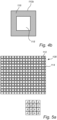
- the pattern comprises blocking areas between the transparent areas, wherein a blocking area at least partially overlaps a light-detecting element so as to limit a portion of the light-detecting element which will receive light through the pattern.
- the blocking area may thus be arranged to limit an amount of light that will reach the light-detecting element by means of the blocking area overlapping the light-detecting element.
- the blocking areas of the pattern are interconnected and the pattern further defines separate transparent areas separated by portions of the blocking areas, wherein each separate transparent area is arranged on the corresponding light-detecting element.
- the light-detecting element may receive light merely at a central part of the light-detecting element, defined by the transparent area. This implies that an area of each light-detecting element in which light will actually be detected is clearly separated from a corresponding light-detecting area of an adjacent light-detecting element. This implies that there is a low risk of cross-talk between the light-detecting elements.
- the transparent areas of the pattern are interconnected and the pattern further defines separate blocking areas separated by portions of the transparent areas, wherein each separate blocking area is arranged on the corresponding light-detecting element.
- each separate blocking area is arranged on the corresponding light-detecting element.
- the imaging sensor may be arranged to reduce a vignetting effect, i.e. that a brightness of an acquired image is reduced at edges of the image due to light being incident on the imaging sensor at different angles.
- the blocking areas are formed of a material which is opaque to wavelengths of light over a total range of wavelengths spanning the wavelength intervals of the array of light-detecting elements. This implies that the blocking areas may be arranged to completely block light over the total range of wavelengths being detected by the light-detecting elements. Hence, the same material of the blocking areas may be used throughout the pattern and the blocking areas may have an equal effect on blocking light for all light-detecting elements.
- the material of the blocking areas need not be completely opaque.
- the material may be arranged to block some light by partially absorbing or reflecting light, while also transmitting some light through the blocking area. Thus, an intensity of light incident on the blocking area may be reduced before reaching the light-detecting element.
- the blocking areas are formed of a material having an equal, or at least substantially equal, transmittance of light over the total range of wavelengths spanning the wavelength intervals of the array of light-detecting elements.
- the blocking areas may have a differing transmittance for different wavelengths.
- the size of the transparent areas may also take into account a transmittance of the blocking area associated with a respective light-detecting element.
- the imaging sensor comprises a filter arranged on the array of light-detecting elements for controlling the respective wavelength interval being detected by the light-detecting elements.
- the filter controls the wavelength being detected by each light-detecting element.
- the pattern may be arranged on the filter, such that the amount of light incident on the filter may be adapted to the sensitivity of the light-detecting element given by the filter.
- the filter comprises Fabry-Perot optical filters being selective to a narrow wavelength interval, wherein a Fabry-Perot optical filter is arranged on each of the light-detecting elements.
- the Fabry-Perot optical filter may thus individually control the wavelength interval being detected by each light-detecting element.
- Each of the wavelength intervals may thus be a narrow wavelength interval, such as having a full-width at half maximum of e.g. 15 nm.
- the filter defines a large number of different wavelength intervals, such as at least four or at least eight, to be detected by the light-detecting elements.
- the use of Fabry-Perot optical filters allows detecting a large number of different wavelength intervals. This implies that the pattern may be advantageously used on a layer providing Fabry-Perot optical filters on the light-detecting elements for controlling an amount of light that reaches the light-detecting elements depending on the wavelength that will be detected by the respective light-detecting element.
- the pattern defines a blocking area corresponding to each light-detecting element, and wherein the blocking area is arranged to block light rays incident on the light-detecting element at smallest angles in relation to a normal to the light-detecting element and wherein a size of the blocking area is dependent of the corresponding light-detecting element with which the blocking area is associated.
- This may be useful in reduction of a vignetting effect, i.e. that a brightness of an acquired image is reduced at edges of the image due to light being incident on the imaging sensor at different angles.
- the blocking area being arranged to block light rays incident at small angles, the difference in brightness at different parts of the array may be reduced.
- a position of the blocking area in relation to the light-detecting element may differ at the center of a row in the array and at the edge of the row in the array.
- the center of the array e.g. at the center of a row of the array, the smallest angle of light rays incident on the light-detecting element will be at the center of the light-detecting element, such that the blocking area may be arranged at a center of the light-detecting element.
- an edge of the array e.g.
- a system for imaging comprising: an optical system for forming an image onto an image plane; and an imaging sensor according to the first aspect arranged in the image plane to acquire an image of an object.
- the system may thus make use of the imaging sensor in order to enable acquiring of an image of an object with a high SNR, spatial resolution, contrast and/or dynamic range.
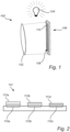
- the system 100 may also comprise an illumination source 104, which provides a known spectral profile of illumination onto the object that is being imaged.
- the system 100 may use an external illumination source, such as by imaging an object under sunlight illumination.
- the system 100 may be adapted to a known spectral profile of the illumination source 104, regardless whether the illumination source is part of the system 100 or not.
- the imaging sensor 106 may be based on a complementary metal-oxide-semiconductor (CMOS) structure.
- CMOS structure may comprise an array 108 of light-detecting elements 110 and may further comprise circuitry e.g. for reading out detected light intensities in the light-detecting elements 110 and for timing accumulation of light in the light-detecting elements.
- the CMOS structure may also comprise circuitry for processing the detected light intensities, such as analog-to-digital converters (ADC) and/or other processing components.
- ADC analog-to-digital converters
- the CMOS structure may thus provide a possibility of detecting light intensities and outputting an image representation, e.g. in the form of digital values of the light intensities detected by each light-detecting element 110 in the array 108.
- the light-detecting elements 110 may be arranged to accumulate charges in dependence of light incident on the light-detecting element 110.
- the light-detecting element 110 may thus comprise e.g. a photodiode or a photo-transistor.
- the array 108 may comprise identical light-detecting elements 110 which are arranged in rows and columns in order to form a two-dimensional array 108.
- the CMOS structure comprising the array 108 may thus be relatively simple and may also be useful for a number of different applications. This implies that chips carrying the array 108 with an associated read-out and control circuitry may be manufactured in large volumes and may therefore be very cheap.
- the imaging sensor 106 may advantageously be formed based on a mass-manufactured CMOS structure.
- the array 108 with associated circuitry may be formed on a substrate, wherein desired functionality of the CMOS structure may be achieved by forming a plurality of layers on the substrate. A thickness of the substrate may then be reduced, such that illumination may fall on the light-detecting elements 110 through the substrate, so-called backside illumination.
- backside illumination This implies that the light will not need to pass layers arranged on the CMOS structure e.g. for readout and, hence, losses of light due to reflections or absorptions in such layers may be avoided.
- backside illumination may provide a possibility to detect as much light as possible, enabling imaging with a high quality.
- the imaging sensor 106 may be specifically adapted with respect to acquiring images with a spectral resolution.
- the imaging sensor 106 may be arranged to detect intensity of light in a plurality of different wavelength intervals and may further be arranged such that light within a wavelength interval is detected by the imaging sensor 106 so as to enable differentiating between varying intensities of light within the wavelength interval over a large span of varying intensities, as will be further described below.
- the imaging sensor 106 may thus be provided with a filter 112 arranged on the array 108 of light-detecting elements 110, e.g. on a front-side of the CMOS structure or a back-side of the CMOS structure depending on whether frontside or backside illumination is used.
- the filter 112 may comprise separate filter portions 112a-c with an individual filter portion for each light-detecting element 110. This implies that the light-detecting element 110a-c will be arranged to detect a wavelength interval defined by the filter portion 112a-c.
- the imaging sensor 106 may be provided with filters in a mosaic configuration, wherein the imaging sensor 106 is divided into identical sub-groups of light-detecting elements 110 repeated over the array 108 of light-detecting elements 110 and wherein a filter 112 is provided with filter portions 112a-c such that a unique wavelength band is transmitted to each light-detecting element 110 in the sub-group.
- each image point (made up by a single sub-group) of an image acquired by the imaging sensor 106 has a spectral resolution defined by the wavelength bands detected in the sub-group.
- each sub-group could be formed by 2x2 or 3x3 light-detecting elements in order to detect four or nine different wavelength bands, respectively.
- the filter portions may be provided as interference filters, wherein a constructive interference of a specific wavelength allows the specific wavelength to be transmitted through the filter portion. This implies that a narrow wavelength band may be transmitted through the filter portion to the light-detecting element 110. Also, by changing for instance a thickness or a material of a layer in the interference filter, a wavelength that is transmitted may be changed. Thus, the filter portions may be used for selectively choosing the wavelength bands that are detected by the light-detecting elements 110 associated with the filter portions.
- the interference filters are provided as Fabry-Perot filters.
- a filter 112 may be associated with the array 108 of light-detecting elements 110 in a different manner.
- the filter portions may for instance not be arranged in a mosaic configuration, such that adjacent light-detecting elements 110 may instead detect a common wavelength band.
- the filter 112 may not need to have very small, separately defined filter portions, which makes manufacture of the filter 112 easier.
- the filter 112 may be arranged in a tiled configuration, where each tile defines a wavelength band and covers a group of light-detecting elements 110 within the array 108.
- the filter 112 may comprise interference filters which may define the wavelength bands detected in the respective tiles.
- the tiles may be relatively large, other filter implementations may also be used, such as using materials or combination of materials being arranged to transmit specific wavelength intervals.
- the tiled configuration may be used in a system 100 comprising an optical duplicator, which is arranged to duplicate an image of an object onto several different portions (tiles) of the imaging sensor 106.
- each tile may acquire an image of the object in a unique wavelength band and the spectral resolution of the imaging sensor is defined by the wavelength bands of the different tiles.
- the filter 112 may according to another alternative be arranged in a different manner to the array 108 of light-detecting elements 110, while providing a fixed relationship between the filter 112 and the array 108.
- the filter 112 need not necessarily be arranged on the same surface as the array 108 of light-detecting elements 110.
- the filter 112 may be mounted in a common housing with the array 108 of light-detecting elements 110, wherein the filter 112 is arranged with a fixed relationship to the array 108 through the mounting of the array 108 and the filter 112 in the common housing.
- the arrangement of the filter 112 in relation to the array 108 may define the wavelength intervals being detected by the respective light-detecting elements 110 of the array 106.
- the system 100 comprises another optical component for controlling a wavelength of light being detected by the light-detecting elements 110.
- the system 100 may comprise a grating, which may direct light in different directions depending on the wavelength.
- the grating may control the wavelength being detected by the respective light-detecting element 110.
- the imaging sensor 106 is thus arranged to detect a plurality of different wavelengths and an image acquired by the imaging sensor 106 thus has a spectral resolution and the imaging sensor 106 is set up such that the wavelength interval being detected by each light-detecting element 110 is well-defined.
- a spectral response of a light-detecting element 110 may not be the same for different wavelengths.
- the sensitivity of a photodiode to incident light may be highly dependent on the wavelength of light.
- a variability in sensitivity limits a possibility to acquire images with same SNR, spatial resolution, contrast and/or dynamic range in all spectral bands using a same exposure time.
- the SNR, spatial resolution, contrast and dynamic range of the image is higher in the spectral bands where the sensitivity is high as small differences in light intensity may be better differentiated and only a small light intensity is required in order for a signal to be above a noise floor.
- the SNR, spatial resolution, contrast and dynamic range improves in the spectral bands with low sensitivity, but the spatial resolution and contrast decreases in the spectral bands with high sensitivity because of saturation in the light-detecting elements 110.
- a variation of a fill factor of light-detecting elements 110 used for detecting each wavelength interval is used.
- the fill factor devoted to wavelength intervals with high sensitivity is reduced while the fill factor devoted to wavelength intervals with low sensitivity is kept as high as possible.
- a central blocking portion may be surrounded by a frame forming a transparent area 118, which may in turn be surrounded by a peripheral blocking portion, such that the central and peripheral blocking portions may together form a blocking area 116 associated with the light-detecting element 110.
- the system 100 for imaging may be especially advantageously used in applications wherein the illumination source 104 will always have the same spectral profile.
- the system 100 may be suitable for use in remote sensing applications, such as satellite- or aircraft-based imaging, wherein sunlight will be used as the illumination source.
- the system 100 may be suitable for use in endoscopic applications, wherein a known illumination source 104 part of the system 100 may be used.
- the pattern 114 may be arranged to address vignetting effects. i.e. that a brightness of an acquired image is reduced at edges of the image due to light being incident on the imaging sensor 106 at different angles.
- the light-detecting elements 110 may be more sensitive to light rays that are on-axis or close to parallel to the optical axis for a number of reasons: the light rays have travelled a short distance; light rays fall onto a small spot in the image plane (at edges of the array 108, the light rays may graze the image plane and spread over a large area); the light rays are not affected by an aperture in the optical system 102. Further, one or more lenses of the optical system 102 may impact light intensity at edges of the array 108 and further add to a vignetting effect.
- the center of the array 108 may be arranged to coincide with an optical axis of the optical system 102.
- the blocking area 116 of the pattern 114 may then be arranged to be larger at a center of the array 108 compared to the blocking area 116 at an edge of the array 108.
- intensity of light at the center of the array is reduced so that the detected intensity of light by light-detecting elements 110 should not be dependent on a position of the light-detecting element 110 in the array 108.
- a position of the blocking area 116 in relation to the light-detecting element 110 may differ depending on the position of the light-detecting element 110 in the array 108. At the center of the array, the smallest angle of light rays incident on the light-detecting element 110 will be at the center of the light-detecting element 110, such that the blocking area 116 may be arranged to cover a center of the light-detecting element 110.
- the smallest angle of light rays incident on the light-detecting element 110 may be at an edge of the light-detecting element 110 closest to the center of the array 108, such that the blocking area 116 may be asymmetrically arranged in relation to the light-detecting element 110 depending on a distance from the light-detecting element 110 to the center of the array 108.
- the system 100 is to be used in a line-scanning application, where an object or a scenery is arranged to be scanned over rows of the array 108 in order to detect different spectral information of the object from different rows, a varying of a size of the blocking areas in one row may be repeated for other rows in the array 108, as a vignetting effect may be handled row by row.
- the rows of the array 108 may extend in a direction perpendicular to a scanning movement direction.
- the pattern 114 may be designed to equalize a SNR, spatial resolution, contrast and/or dynamic range for different wavelengths and to reduce a vignetting effect.
- a size of blocking areas 116 and transparent areas 118 may be dependent on both these effects.
Landscapes
- Physics & Mathematics (AREA)
- Spectroscopy & Molecular Physics (AREA)
- General Physics & Mathematics (AREA)
- Spectrometry And Color Measurement (AREA)
- Solid State Image Pick-Up Elements (AREA)
Claims (12)
- Bildgebungssensor, umfassend:eine Anordnung (108) von lichtdetektierenden Elementen (110), wobei die Anordnung (108) von lichtdetektierenden Elementen (110) identische lichtdetektierende Elemente (110) in der ganzen Anordnung (108) umfasst, wobei jedes lichtdetektierende Element (110) in der Anordnung (108) von lichtdetektierenden Elementen (110) in dem Bildgebungssensor (106) derart angeordnet ist, dass es ein jeweiliges Wellenlängenintervall detektiert, wobei das jeweilige Wellenlängenintervall für verschiedene lichtdetektierende Elemente unterschiedlich ist;ein Filter (112), das in der Anordnung (108) von lichtdetektierenden Elementen (110) angeordnet ist, um das jeweilige Wellenlängenintervall zu steuern, das von den lichtdetektierenden Elementen (110) detektiert wird; undein Muster (114), das in der Anordnung (108) von lichtdetektierenden Elementen (110) angeordnet ist, wobei das Muster (114) eine Vielzahl von durchsichtigen Bereichen (118) definiert, wobei jeder durchsichtige Bereich (118) einem entsprechenden lichtdetektierenden Element (110) in der Anordnung (108) von lichtdetektierenden Elementen (110) zugeordnet ist,dadurch gekennzeichnet, dass das Muster (114) in die Anordnung (108) von lichtdetektierenden Elementen (110) durch Abscheiden und Ätzen von Material auf der Anordnung (108) von lichtdetektierenden Elementen (110) integriert ist, wobei eine Größe eines durchsichtigen Bereichs (118) aus der Vielzahl von durchsichtigen Bereichen (118) von dem Wellenlängenintervall des entsprechenden lichtdetektierenden Elements (110), dem der durchsichtige Bereich (118) zugeordnet ist, abhängig ist; wobei sich die Größen von mindestens zwei durchsichtigen Bereichen (118) aus der Vielzahl von durchsichtigen Bereichen (118) voneinander unterscheiden.
- Bildgebungssensor nach Anspruch 1, wobei ein erstes lichtdetektierendes Element, das eine geringste Empfindlichkeit für das jeweilige Intervall von Wellenlängen aufweist, zum Definieren einer maximalen Größe des durchsichtigen Bereichs (118) des Musters (114) verwendet wird, und wobei die durchsichtigen Bereiche (118) anderer lichtdetektierender Elemente kleiner als die maximale Größe sind und dazu ausgelegt sind, mindestens eines von einem Signal-Rausch-Verhältnis, einem Kontrast und einem Dynamikbereich einzustellen, damit es für die lichtdetektierenden Elemente gleich ist.
- Bildgebungssensor nach einem der vorhergehenden Ansprüche, wobei das Muster (114) Blockierungsbereiche (116) zwischen den durchsichtigen Bereichen (118) umfasst, wobei sich ein Blockierungsbereich (116) mindestens teilweise mit einem lichtdetektierenden Element (110) überlappt, um einen Abschnitt des lichtdetektierenden Elements (110) einzuschränken, der Licht durch das Muster (114) hindurch empfängt.
- Bildgebungssensor nach Anspruch 3, wobei die Blockierungsbereiche (116) des Musters (114) miteinander verbunden sind, und das Muster (114) ferner getrennte durchsichtige Bereiche (118) definiert, die durch Abschnitte der Blockierungsbereiche (116) getrennt sind, wobei jeder getrennte durchsichtige Bereich (118) auf dem entsprechenden lichtdetektierenden Element (110) angeordnet ist.
- Bildgebungssensor nach Anspruch 3, wobei die durchsichtigen Bereiche (118) des Musters (114) miteinander verbunden sind, und das Muster (114) ferner getrennte Blockierungsbereiche (116) definiert, die durch Abschnitte der durchsichtigen Bereiche (118) getrennt sind, wobei jeder getrennte Blockierungsbereich (116) auf dem entsprechenden lichtdetektierenden Element (110) angeordnet ist.
- Bildgebungssensor nach einem der Ansprüche 3 bis 5, wobei die Blockierungsbereiche (116) aus einem Material gebildet sind, das für die Wellenlängen von Licht über einen Gesamtbereich von Wellenlängen, der die Wellenlängenintervalle der Anordnung (108) von lichtdetektierenden Elementen (110) umfasst, undurchsichtig sind.
- Bildgebungssensor nach einem der vorhergehenden Ansprüche, wobei das Filter (112) optische Fabry-Perot-Filter umfasst, die für ein schmales Wellenlängenintervall selektiv sind, wobei ein optisches Fabry-Perot-Filter an jedem der lichtdetektierenden Elemente (110) angeordnet ist.
- Bildgebungssensor nach einem der vorhergehenden Ansprüche, wobei das Filter (112) eine große Anzahl von verschiedenen Wellenlängenintervallen definiert, wie etwa mindestens vier oder mindestens acht, die von den lichtdetektierenden Elementen zu detektieren sind.
- Bildgebungssensor nach einem der vorhergehenden Ansprüche, wobei der Bildgebungssensor (106) zur rückseitigen Beleuchtung angeordnet ist.
- System zur Bildgebung, umfassend:ein optisches System (102) zum Formen eines Bildes auf einer Bildebene; undeinen Bildgebungssensor (106) nach einem der vorhergehenden Ansprüche, der in der Bildebene angeordnet ist, um ein Bild eines Objekts zu erfassen.
- System nach Anspruch 10, wobei die Größen der durchsichtigen Bereiche (118) des Bildgebungssensors (106) mit Bezug auf ein Spektralprofil einer Beleuchtungsquelle (104) ausgelegt sind.
- Verwendung eines Bildgebungssensors nach einem der Ansprüche 1 bis 9 zum Erfassen eines Bildes, das einen konstanten Bildgebungsparameter über einen Bereich von Wellenlängen aufweist, der die Wellenlängenintervalle der lichtdetektierenden Elementen (110) umfasst, wobei der Bildgebungsparameter mindestens einer von einem Signal-Rausch-Verhältnis, einem Kontrast und einem Dynamikbereich ist.
Applications Claiming Priority (1)
| Application Number | Priority Date | Filing Date | Title |
|---|---|---|---|
| EP16206580 | 2016-12-23 |
Publications (2)
| Publication Number | Publication Date |
|---|---|
| EP3339821A1 EP3339821A1 (de) | 2018-06-27 |
| EP3339821B1 true EP3339821B1 (de) | 2025-04-16 |
Family
ID=57714444
Family Applications (1)
| Application Number | Title | Priority Date | Filing Date |
|---|---|---|---|
| EP17205057.7A Active EP3339821B1 (de) | 2016-12-23 | 2017-12-04 | Bildsensor |
Country Status (2)
| Country | Link |
|---|---|
| US (1) | US11244977B2 (de) |
| EP (1) | EP3339821B1 (de) |
Families Citing this family (7)
| Publication number | Priority date | Publication date | Assignee | Title |
|---|---|---|---|---|
| US10620054B2 (en) * | 2018-05-09 | 2020-04-14 | Wisconsin Alumni Research Foundation | Wavefront detector |
| US12372404B2 (en) | 2020-07-01 | 2025-07-29 | Spectricity | Illuminant correction in an imaging system |
| US11696043B2 (en) * | 2020-07-01 | 2023-07-04 | Spectricity | White balance compensation using a spectral sensor system |
| CN113643673B (zh) * | 2021-07-22 | 2022-11-01 | 武汉华星光电技术有限公司 | 环境光检测方法及装置、显示装置 |
| CN115995473A (zh) * | 2021-10-18 | 2023-04-21 | 天津津航技术物理研究所 | 宽自由光谱范围多光谱成像芯片结构的制备方法 |
| US12487119B2 (en) | 2023-01-09 | 2025-12-02 | Nanohmics, Inc. | Integral field spectral imager |
| WO2024156637A1 (en) | 2023-01-23 | 2024-08-02 | Trinamix Gmbh | Method for arranging an optical measurement device |
Citations (1)
| Publication number | Priority date | Publication date | Assignee | Title |
|---|---|---|---|---|
| EP2937903A1 (de) * | 2014-04-23 | 2015-10-28 | Goodrich Corporation | Maskierte pixelarrays |
Family Cites Families (11)
| Publication number | Priority date | Publication date | Assignee | Title |
|---|---|---|---|---|
| US6429036B1 (en) | 1999-01-14 | 2002-08-06 | Micron Technology, Inc. | Backside illumination of CMOS image sensor |
| TWM249381U (en) | 2003-12-19 | 2004-11-01 | Hon Hai Prec Ind Co Ltd | Image sensor |
| KR100976284B1 (ko) * | 2007-06-07 | 2010-08-16 | 가부시끼가이샤 도시바 | 촬상 장치 |
| FR2926635B1 (fr) * | 2008-01-21 | 2012-08-03 | Silios Technologies | Dispositif de spectroscopie en longueur d'onde a filtres integres |
| EP2243011A4 (de) * | 2008-02-13 | 2013-12-18 | Hewlett Packard Co | Farbdetektor mit flächenskalierten fotodetektoren |
| JP2010093081A (ja) * | 2008-10-08 | 2010-04-22 | Panasonic Corp | 固体撮像装置およびその製造方法 |
| US8314866B2 (en) | 2010-04-06 | 2012-11-20 | Omnivision Technologies, Inc. | Imager with variable area color filter array and pixel elements |
| FR2974669B1 (fr) * | 2011-04-28 | 2013-06-07 | Commissariat Energie Atomique | Dispositif imageur destine a evaluer des distances d'elements dans une image |
| US8940574B2 (en) | 2012-04-17 | 2015-01-27 | Taiwan Semiconductor Manufacturing Company, Ltd. | Metal grid in backside illumination image sensor chips and methods for forming the same |
| US9253420B2 (en) * | 2014-02-12 | 2016-02-02 | Xerox Corporation | Hyperspectral single pixel imager with fabry perot filter |
| JP2015230950A (ja) * | 2014-06-04 | 2015-12-21 | 住友電気工業株式会社 | アレイ型受光素子 |
-
2017
- 2017-12-04 EP EP17205057.7A patent/EP3339821B1/de active Active
- 2017-12-19 US US15/846,584 patent/US11244977B2/en active Active
Patent Citations (1)
| Publication number | Priority date | Publication date | Assignee | Title |
|---|---|---|---|---|
| EP2937903A1 (de) * | 2014-04-23 | 2015-10-28 | Goodrich Corporation | Maskierte pixelarrays |
Also Published As
| Publication number | Publication date |
|---|---|
| US11244977B2 (en) | 2022-02-08 |
| EP3339821A1 (de) | 2018-06-27 |
| US20180182798A1 (en) | 2018-06-28 |
Similar Documents
| Publication | Publication Date | Title |
|---|---|---|
| EP3339821B1 (de) | Bildsensor | |
| US7858921B2 (en) | Guided-mode-resonance transmission color filters for color generation in CMOS image sensors | |
| US9888194B2 (en) | Array camera architecture implementing quantum film image sensors | |
| JP5331107B2 (ja) | 撮像装置 | |
| EP3633334B1 (de) | Spektralsensor zur multispektralen bildgebung | |
| JP6144321B2 (ja) | カラーエイリアシングを最小化するrgbcカラーフィルタアレイのパターン | |
| US8546737B2 (en) | Systems and methods for color binning | |
| US9596423B1 (en) | Charge summing in an image sensor | |
| EP3450938B1 (de) | Bildsensor und bildgebungsvorrichtung | |
| CN106612420B (zh) | 彩色滤光器阵列及图像传感器 | |
| US20170347042A1 (en) | Imaging systems with high dynamic range and phase detection pixels | |
| US20110317048A1 (en) | Image sensor with dual layer photodiode structure | |
| US20180204863A1 (en) | Image sensor, an imaging device, an imaging system and a method for spectral imaging | |
| US9945718B2 (en) | Image sensors with multi-functional pixel clusters | |
| KR20090067059A (ko) | 디지털 이미지를 생성하는 방법 및 장치 | |
| KR20130136372A (ko) | 이미저 어레이 구조 및 어레이 카메라 | |
| EP3465113B1 (de) | Kombinagtion aus spektralmessung und bildgebungssensor | |
| US20220130879A1 (en) | Image sensor and imaging apparatus | |
| JP2006165362A (ja) | 固体撮像素子 | |
| US7053998B2 (en) | Photo-detector filter | |
| US20240151884A1 (en) | Pixel having light focusing transparent diffractive grating | |
| US7929126B2 (en) | Photo-detector filter | |
| US6744032B1 (en) | Arrangement of microlenses in a solid-state image sensor for improving signal to noise ratio | |
| KR101473720B1 (ko) | 컬러 필터 어레이 및 컬러 필터 제조 방법, 및 상기 컬러필터 어레이를 포함하는 이미지 촬상 장치 | |
| US20250287081A1 (en) | Hyperspectral sensor with diffractive focusing pixel and neural network spectral recovery |
Legal Events
| Date | Code | Title | Description |
|---|---|---|---|
| PUAI | Public reference made under article 153(3) epc to a published international application that has entered the european phase |
Free format text: ORIGINAL CODE: 0009012 |
|
| STAA | Information on the status of an ep patent application or granted ep patent |
Free format text: STATUS: THE APPLICATION HAS BEEN PUBLISHED |
|
| AK | Designated contracting states |
Kind code of ref document: A1 Designated state(s): AL AT BE BG CH CY CZ DE DK EE ES FI FR GB GR HR HU IE IS IT LI LT LU LV MC MK MT NL NO PL PT RO RS SE SI SK SM TR |
|
| AX | Request for extension of the european patent |
Extension state: BA ME |
|
| STAA | Information on the status of an ep patent application or granted ep patent |
Free format text: STATUS: REQUEST FOR EXAMINATION WAS MADE |
|
| 17P | Request for examination filed |
Effective date: 20181221 |
|
| RBV | Designated contracting states (corrected) |
Designated state(s): AL AT BE BG CH CY CZ DE DK EE ES FI FR GB GR HR HU IE IS IT LI LT LU LV MC MK MT NL NO PL PT RO RS SE SI SK SM TR |
|
| STAA | Information on the status of an ep patent application or granted ep patent |
Free format text: STATUS: EXAMINATION IS IN PROGRESS |
|
| 17Q | First examination report despatched |
Effective date: 20210809 |
|
| GRAP | Despatch of communication of intention to grant a patent |
Free format text: ORIGINAL CODE: EPIDOSNIGR1 |
|
| STAA | Information on the status of an ep patent application or granted ep patent |
Free format text: STATUS: GRANT OF PATENT IS INTENDED |
|
| INTG | Intention to grant announced |
Effective date: 20241114 |
|
| GRAS | Grant fee paid |
Free format text: ORIGINAL CODE: EPIDOSNIGR3 |
|
| GRAA | (expected) grant |
Free format text: ORIGINAL CODE: 0009210 |
|
| STAA | Information on the status of an ep patent application or granted ep patent |
Free format text: STATUS: THE PATENT HAS BEEN GRANTED |
|
| AK | Designated contracting states |
Kind code of ref document: B1 Designated state(s): AL AT BE BG CH CY CZ DE DK EE ES FI FR GB GR HR HU IE IS IT LI LT LU LV MC MK MT NL NO PL PT RO RS SE SI SK SM TR |
|
| REG | Reference to a national code |
Ref country code: GB Ref legal event code: FG4D |
|
| REG | Reference to a national code |
Ref country code: CH Ref legal event code: EP Ref country code: DE Ref legal event code: R096 Ref document number: 602017088920 Country of ref document: DE |
|
| P01 | Opt-out of the competence of the unified patent court (upc) registered |
Free format text: CASE NUMBER: APP_14881/2025 Effective date: 20250327 |
|
| REG | Reference to a national code |
Ref country code: IE Ref legal event code: FG4D |
|
| REG | Reference to a national code |
Ref country code: NL Ref legal event code: MP Effective date: 20250416 |
|
| PG25 | Lapsed in a contracting state [announced via postgrant information from national office to epo] |
Ref country code: NL Free format text: LAPSE BECAUSE OF FAILURE TO SUBMIT A TRANSLATION OF THE DESCRIPTION OR TO PAY THE FEE WITHIN THE PRESCRIBED TIME-LIMIT Effective date: 20250416 |
|
| REG | Reference to a national code |
Ref country code: AT Ref legal event code: MK05 Ref document number: 1785978 Country of ref document: AT Kind code of ref document: T Effective date: 20250416 |
|
| PG25 | Lapsed in a contracting state [announced via postgrant information from national office to epo] |
Ref country code: PT Free format text: LAPSE BECAUSE OF FAILURE TO SUBMIT A TRANSLATION OF THE DESCRIPTION OR TO PAY THE FEE WITHIN THE PRESCRIBED TIME-LIMIT Effective date: 20250818 Ref country code: FI Free format text: LAPSE BECAUSE OF FAILURE TO SUBMIT A TRANSLATION OF THE DESCRIPTION OR TO PAY THE FEE WITHIN THE PRESCRIBED TIME-LIMIT Effective date: 20250416 Ref country code: ES Free format text: LAPSE BECAUSE OF FAILURE TO SUBMIT A TRANSLATION OF THE DESCRIPTION OR TO PAY THE FEE WITHIN THE PRESCRIBED TIME-LIMIT Effective date: 20250416 |
|
| REG | Reference to a national code |
Ref country code: LT Ref legal event code: MG9D |
|
| PG25 | Lapsed in a contracting state [announced via postgrant information from national office to epo] |
Ref country code: NO Free format text: LAPSE BECAUSE OF FAILURE TO SUBMIT A TRANSLATION OF THE DESCRIPTION OR TO PAY THE FEE WITHIN THE PRESCRIBED TIME-LIMIT Effective date: 20250716 Ref country code: GR Free format text: LAPSE BECAUSE OF FAILURE TO SUBMIT A TRANSLATION OF THE DESCRIPTION OR TO PAY THE FEE WITHIN THE PRESCRIBED TIME-LIMIT Effective date: 20250717 |
|
| PG25 | Lapsed in a contracting state [announced via postgrant information from national office to epo] |
Ref country code: PL Free format text: LAPSE BECAUSE OF FAILURE TO SUBMIT A TRANSLATION OF THE DESCRIPTION OR TO PAY THE FEE WITHIN THE PRESCRIBED TIME-LIMIT Effective date: 20250416 |
|
| PG25 | Lapsed in a contracting state [announced via postgrant information from national office to epo] |
Ref country code: BG Free format text: LAPSE BECAUSE OF FAILURE TO SUBMIT A TRANSLATION OF THE DESCRIPTION OR TO PAY THE FEE WITHIN THE PRESCRIBED TIME-LIMIT Effective date: 20250416 |
|
| PG25 | Lapsed in a contracting state [announced via postgrant information from national office to epo] |
Ref country code: HR Free format text: LAPSE BECAUSE OF FAILURE TO SUBMIT A TRANSLATION OF THE DESCRIPTION OR TO PAY THE FEE WITHIN THE PRESCRIBED TIME-LIMIT Effective date: 20250416 |
|
| PG25 | Lapsed in a contracting state [announced via postgrant information from national office to epo] |
Ref country code: AT Free format text: LAPSE BECAUSE OF FAILURE TO SUBMIT A TRANSLATION OF THE DESCRIPTION OR TO PAY THE FEE WITHIN THE PRESCRIBED TIME-LIMIT Effective date: 20250416 |
|
| PG25 | Lapsed in a contracting state [announced via postgrant information from national office to epo] |
Ref country code: RS Free format text: LAPSE BECAUSE OF FAILURE TO SUBMIT A TRANSLATION OF THE DESCRIPTION OR TO PAY THE FEE WITHIN THE PRESCRIBED TIME-LIMIT Effective date: 20250716 |
|
| PG25 | Lapsed in a contracting state [announced via postgrant information from national office to epo] |
Ref country code: IS Free format text: LAPSE BECAUSE OF FAILURE TO SUBMIT A TRANSLATION OF THE DESCRIPTION OR TO PAY THE FEE WITHIN THE PRESCRIBED TIME-LIMIT Effective date: 20250816 |
|
| PG25 | Lapsed in a contracting state [announced via postgrant information from national office to epo] |
Ref country code: LV Free format text: LAPSE BECAUSE OF FAILURE TO SUBMIT A TRANSLATION OF THE DESCRIPTION OR TO PAY THE FEE WITHIN THE PRESCRIBED TIME-LIMIT Effective date: 20250416 |
|
| PGFP | Annual fee paid to national office [announced via postgrant information from national office to epo] |
Ref country code: DE Payment date: 20251126 Year of fee payment: 9 |
|
| PG25 | Lapsed in a contracting state [announced via postgrant information from national office to epo] |
Ref country code: SM Free format text: LAPSE BECAUSE OF FAILURE TO SUBMIT A TRANSLATION OF THE DESCRIPTION OR TO PAY THE FEE WITHIN THE PRESCRIBED TIME-LIMIT Effective date: 20250416 Ref country code: DK Free format text: LAPSE BECAUSE OF FAILURE TO SUBMIT A TRANSLATION OF THE DESCRIPTION OR TO PAY THE FEE WITHIN THE PRESCRIBED TIME-LIMIT Effective date: 20250416 |
|
| REG | Reference to a national code |
Ref country code: DE Ref legal event code: R097 Ref document number: 602017088920 Country of ref document: DE |
|
| PG25 | Lapsed in a contracting state [announced via postgrant information from national office to epo] |
Ref country code: CZ Free format text: LAPSE BECAUSE OF FAILURE TO SUBMIT A TRANSLATION OF THE DESCRIPTION OR TO PAY THE FEE WITHIN THE PRESCRIBED TIME-LIMIT Effective date: 20250416 |
|
| PG25 | Lapsed in a contracting state [announced via postgrant information from national office to epo] |
Ref country code: EE Free format text: LAPSE BECAUSE OF FAILURE TO SUBMIT A TRANSLATION OF THE DESCRIPTION OR TO PAY THE FEE WITHIN THE PRESCRIBED TIME-LIMIT Effective date: 20250416 |
|
| PG25 | Lapsed in a contracting state [announced via postgrant information from national office to epo] |
Ref country code: SK Free format text: LAPSE BECAUSE OF FAILURE TO SUBMIT A TRANSLATION OF THE DESCRIPTION OR TO PAY THE FEE WITHIN THE PRESCRIBED TIME-LIMIT Effective date: 20250416 Ref country code: RO Free format text: LAPSE BECAUSE OF FAILURE TO SUBMIT A TRANSLATION OF THE DESCRIPTION OR TO PAY THE FEE WITHIN THE PRESCRIBED TIME-LIMIT Effective date: 20250416 |
|
| PG25 | Lapsed in a contracting state [announced via postgrant information from national office to epo] |
Ref country code: IT Free format text: LAPSE BECAUSE OF FAILURE TO SUBMIT A TRANSLATION OF THE DESCRIPTION OR TO PAY THE FEE WITHIN THE PRESCRIBED TIME-LIMIT Effective date: 20250416 |
|
| PLBE | No opposition filed within time limit |
Free format text: ORIGINAL CODE: 0009261 |
|
| STAA | Information on the status of an ep patent application or granted ep patent |
Free format text: STATUS: NO OPPOSITION FILED WITHIN TIME LIMIT |
|
| REG | Reference to a national code |
Ref country code: CH Ref legal event code: L10 Free format text: ST27 STATUS EVENT CODE: U-0-0-L10-L00 (AS PROVIDED BY THE NATIONAL OFFICE) Effective date: 20260225 |
|
| 26N | No opposition filed |
Effective date: 20260119 |