EP3340226A1 - Procédé de pilotage d'affichage - Google Patents
Procédé de pilotage d'affichage Download PDFInfo
- Publication number
- EP3340226A1 EP3340226A1 EP16837348.8A EP16837348A EP3340226A1 EP 3340226 A1 EP3340226 A1 EP 3340226A1 EP 16837348 A EP16837348 A EP 16837348A EP 3340226 A1 EP3340226 A1 EP 3340226A1
- Authority
- EP
- European Patent Office
- Prior art keywords
- level
- blue
- red
- green
- pixel
- Prior art date
- Legal status (The legal status is an assumption and is not a legal conclusion. Google has not performed a legal analysis and makes no representation as to the accuracy of the status listed.)
- Withdrawn
Links
Images


Classifications
-
- G—PHYSICS
- G09—EDUCATION; CRYPTOGRAPHY; DISPLAY; ADVERTISING; SEALS
- G09G—ARRANGEMENTS OR CIRCUITS FOR CONTROL OF INDICATING DEVICES USING STATIC MEANS TO PRESENT VARIABLE INFORMATION
- G09G3/00—Control arrangements or circuits, of interest only in connection with visual indicators other than cathode-ray tubes
- G09G3/20—Control arrangements or circuits, of interest only in connection with visual indicators other than cathode-ray tubes for presentation of an assembly of a number of characters, e.g. a page, by composing the assembly by combination of individual elements arranged in a matrix no fixed position being assigned to or needed to be assigned to the individual characters or partial characters
- G09G3/22—Control arrangements or circuits, of interest only in connection with visual indicators other than cathode-ray tubes for presentation of an assembly of a number of characters, e.g. a page, by composing the assembly by combination of individual elements arranged in a matrix no fixed position being assigned to or needed to be assigned to the individual characters or partial characters using controlled light sources
- G09G3/30—Control arrangements or circuits, of interest only in connection with visual indicators other than cathode-ray tubes for presentation of an assembly of a number of characters, e.g. a page, by composing the assembly by combination of individual elements arranged in a matrix no fixed position being assigned to or needed to be assigned to the individual characters or partial characters using controlled light sources using electroluminescent panels
- G09G3/32—Control arrangements or circuits, of interest only in connection with visual indicators other than cathode-ray tubes for presentation of an assembly of a number of characters, e.g. a page, by composing the assembly by combination of individual elements arranged in a matrix no fixed position being assigned to or needed to be assigned to the individual characters or partial characters using controlled light sources using electroluminescent panels semiconductive, e.g. using light-emitting diodes [LED]
-
- G—PHYSICS
- G09—EDUCATION; CRYPTOGRAPHY; DISPLAY; ADVERTISING; SEALS
- G09G—ARRANGEMENTS OR CIRCUITS FOR CONTROL OF INDICATING DEVICES USING STATIC MEANS TO PRESENT VARIABLE INFORMATION
- G09G3/00—Control arrangements or circuits, of interest only in connection with visual indicators other than cathode-ray tubes
- G09G3/20—Control arrangements or circuits, of interest only in connection with visual indicators other than cathode-ray tubes for presentation of an assembly of a number of characters, e.g. a page, by composing the assembly by combination of individual elements arranged in a matrix no fixed position being assigned to or needed to be assigned to the individual characters or partial characters
- G09G3/34—Control arrangements or circuits, of interest only in connection with visual indicators other than cathode-ray tubes for presentation of an assembly of a number of characters, e.g. a page, by composing the assembly by combination of individual elements arranged in a matrix no fixed position being assigned to or needed to be assigned to the individual characters or partial characters by control of light from an independent source
-
- H—ELECTRICITY
- H10—SEMICONDUCTOR DEVICES; ELECTRIC SOLID-STATE DEVICES NOT OTHERWISE PROVIDED FOR
- H10H—INORGANIC LIGHT-EMITTING SEMICONDUCTOR DEVICES HAVING POTENTIAL BARRIERS
- H10H20/00—Individual inorganic light-emitting semiconductor devices having potential barriers, e.g. light-emitting diodes [LED]
- H10H20/80—Constructional details
-
- H—ELECTRICITY
- H10—SEMICONDUCTOR DEVICES; ELECTRIC SOLID-STATE DEVICES NOT OTHERWISE PROVIDED FOR
- H10H—INORGANIC LIGHT-EMITTING SEMICONDUCTOR DEVICES HAVING POTENTIAL BARRIERS
- H10H20/00—Individual inorganic light-emitting semiconductor devices having potential barriers, e.g. light-emitting diodes [LED]
- H10H20/80—Constructional details
- H10H20/81—Bodies
- H10H20/813—Bodies having a plurality of light-emitting regions, e.g. multi-junction LEDs or light-emitting devices having photoluminescent regions within the bodies
-
- H—ELECTRICITY
- H10—SEMICONDUCTOR DEVICES; ELECTRIC SOLID-STATE DEVICES NOT OTHERWISE PROVIDED FOR
- H10H—INORGANIC LIGHT-EMITTING SEMICONDUCTOR DEVICES HAVING POTENTIAL BARRIERS
- H10H20/00—Individual inorganic light-emitting semiconductor devices having potential barriers, e.g. light-emitting diodes [LED]
- H10H20/80—Constructional details
- H10H20/83—Electrodes
-
- H—ELECTRICITY
- H10—SEMICONDUCTOR DEVICES; ELECTRIC SOLID-STATE DEVICES NOT OTHERWISE PROVIDED FOR
- H10K—ORGANIC ELECTRIC SOLID-STATE DEVICES
- H10K59/00—Integrated devices, or assemblies of multiple devices, comprising at least one organic light-emitting element covered by group H10K50/00
- H10K59/10—OLED displays
-
- H—ELECTRICITY
- H10—SEMICONDUCTOR DEVICES; ELECTRIC SOLID-STATE DEVICES NOT OTHERWISE PROVIDED FOR
- H10K—ORGANIC ELECTRIC SOLID-STATE DEVICES
- H10K59/00—Integrated devices, or assemblies of multiple devices, comprising at least one organic light-emitting element covered by group H10K50/00
- H10K59/30—Devices specially adapted for multicolour light emission
- H10K59/35—Devices specially adapted for multicolour light emission comprising red-green-blue [RGB] subpixels
-
- G—PHYSICS
- G09—EDUCATION; CRYPTOGRAPHY; DISPLAY; ADVERTISING; SEALS
- G09G—ARRANGEMENTS OR CIRCUITS FOR CONTROL OF INDICATING DEVICES USING STATIC MEANS TO PRESENT VARIABLE INFORMATION
- G09G2310/00—Command of the display device
- G09G2310/02—Addressing, scanning or driving the display screen or processing steps related thereto
- G09G2310/0264—Details of driving circuits
-
- G—PHYSICS
- G09—EDUCATION; CRYPTOGRAPHY; DISPLAY; ADVERTISING; SEALS
- G09G—ARRANGEMENTS OR CIRCUITS FOR CONTROL OF INDICATING DEVICES USING STATIC MEANS TO PRESENT VARIABLE INFORMATION
- G09G3/00—Control arrangements or circuits, of interest only in connection with visual indicators other than cathode-ray tubes
- G09G3/20—Control arrangements or circuits, of interest only in connection with visual indicators other than cathode-ray tubes for presentation of an assembly of a number of characters, e.g. a page, by composing the assembly by combination of individual elements arranged in a matrix no fixed position being assigned to or needed to be assigned to the individual characters or partial characters
- G09G3/2007—Display of intermediate tones
- G09G3/2014—Display of intermediate tones by modulation of the duration of a single pulse during which the logic level remains constant
Definitions
- the present invention relates to a method of driving a display using a light emitting diode, and more particularly, to a method of driving a display capable of controlling color light combination and luminance of the display by controlling light emitting time for illuminating a multi-junction light emitting diode.
- a light emitting diode is developed and used as a display light source of various devices, and a light source thereof has straightness, low power consumption, and long lifetime.
- a high brightness light emitting diode is manufactured and used.
- the high brightness light emitting diode is very efficiently used for a safety display illumination of a portable illumination such as a flash light, a bicycle, etc.
- a safety display illumination such as a flash light, a bicycle, etc.
- the integrated high brightness light emitting diodes can be used as a illumination lamp of high luminance.
- the above-described light emitting diode is widely practicalized as a stand device of an illumination device used for studying, reading, etc., a mood lamp device installed on a wall for illuminating and for scenery of indoor or outdoor, a sensor illumination lamp device of an entrance, etc.
- Methods for driving the light emitting diode as a light emitting device include a voltage control method and a current control method.
- a voltage control method or the current control method a predetermined voltage or a predetermined current is applied to the light emitting diode, and thus, the voltage control method or the current control method maintains a particular color or a luminance.
- a nitride semiconductor device has an unstable ratio between efficiency and current. Thus, when a device is operated by a current of maximum efficiency, the efficiency is decreased.
- the purpose of the present invention is to provide a method of driving a display at a maximum efficiency of the display by controlling a light emitting time for illumination of a light emitting diode using a pulse width modulation control method to maximize efficiency of the display.
- a driving pulse of a pulse width modulation method is applied to each pixel by a drive circuit, and a time for illuminating a red light, a blue light, and a green light, which are three primary colors, of each pixel is controlled, thereby controlling the luminance of the pixel.
- a refresh cycle for illuminating the pixel may include a plurality of levels.
- the red, green, and blue of the pixel in each refresh cycle may have one level selected from a minimum level to a maximum level.
- Luminance of the pixel may be determined by combination of the red, blue, and green illuminated based on the times for illumination in the refresh period.
- the drive circuit may apply a signal of a low level within a time corresponding to the minimum level to control the times for illuminating the red, blue, and green.
- the times for illuminating the red, blue, and green may be simultaneously controlled by one drive circuit.
- the times for illuminating the red, blue, and green may be controlled by three drive circuits, respectively.
- the light emitting diode may include a multi junction light emitting diode (MJ LED), in which a plurality of layers illuminating different colors are combined.
- MJ LED multi junction light emitting diode
- illumination time of each of three primary colors of light on each pixel is increased or decreased using a pulse width modulation method to control luminance of each pixel to control luminance of each pixel, and thus, luminance change caused by current change in a conventional current control method may be prevented.
- the display may be operated at a current of the maximum efficiency, and thus, efficiency of the display may be maximized.
- FIG. 1 is a cross-sectional view illustrating a light emitting diode having a multi-junction structure according to one embodiment of the present invention.
- the light emitting diode includes a plurality of light emitting structures 200 formed on a substrate 100.
- Each of the light emitting structures 200 includes a first n-type semiconductor layer 210, a first light emitting layer 220, a p-type semiconductor layer 230, a second light emitting layer 240, and a second n-type semiconductor layer 250.
- electrodes 310, 320, and 330 are connected to each of the light emitting structures 200.
- the electrodes include a first n-type electrode 310, a p-type electrode 320, and a second n-type electrode 330.
- the first n-type electrode 310 is electrically connected to the first n-type semiconductor layer 210
- the p-type electrode 320 is electrically connected to the p-type semiconductor layer 230
- the second n-type electrode 330 is electrically connected to the second n-type semiconductor layer 250.
- the p-type electrode 320 is formed in a separate space formed by the light emitting structures 200, and makes contact with a side surface of the p-type semiconductor layer 230.
- the first n-type semiconductor layer 210 is formed on the substrate 100.
- the substrate 100 may be changed based on material of the first n-type semiconductor layer 210.
- the substrate 100 may include sapphire, gallium nitride, or zinc oxide.
- the doping donors are determined by the material of the first n-type semiconductor layer 210.
- the first light emitting layer 220 is formed on the first n-type semiconductor layer 210.
- the first light emitting layer 220 may include a barrier layer and a well layer, which are alternately formed.
- the barrier layer may preferably include gallium nitride.
- the p-type semiconductor layer 230 is formed on the first light emitting layer 220. Acceptors are doped in the p-type semiconductor layer 230. The doping acceptors may be variously selected based on material of the p-type semiconductor layer 230.
- the second light emitting layer 240 is formed on the p-type semiconductor layer 230.
- the second light emitting layer 240 may include a barrier layer and a well layer, which are alternately formed, and may be formed of the same material as the first light emitting layer 220.
- a bandgap engineering which is different from that of the first light emitting layer 220, may be performed on the second light emitting layer 240.
- the first light emitting layer 220 may generate light of a first color based on content of induced indium
- the second light emitting layer 240 may generate light of a second color, which is different from the first color.
- the second n-type semiconductor layer 250 may be formed on the second light emitting layer 240.
- the second n-type semiconductor layer 250 may have the same composition as the first n-type semiconductor layer 210.
- the first n-type electrode 310 is formed on a side surface or an upper surface of the first n-type semiconductor layer 210. Also, a first passivation layer 410 is formed on the first n-type electrode 310, and the p-type electrode 320 is formed on an upper surface of the first passivation layer 410 and a side surface of the p-type semiconductor layer 230. Also, a second passivation layer 420 is formed on the p-type electrode 320, and the second n-type electrode 330 may be formed on an upper surface of the second passivation layer 420 or a side surface of the second n-type semiconductor layer.
- the uppermost surface of the second passivation layer 420 is not higher than the surface of the second n-type semiconductor layer 250.
- the first n-type semiconductor layers 210 of the light emitting structures 200 are electrically connected to each other.
- the first n-type electrode 310 electrically connected to the first n-type semiconductor layer 210 is electrically connected to the first n-type semiconductor later 210 of the light emitting structure 200.
- the p-type electrode 320 formed on the first passivation layer 410 makes contact with a side surface of the p-type semiconductor layer 220.
- the second n-type electrode 330 is electrically connected to the second n-type semiconductor later 250.
- the plurality of light emitting structures 200 are connected to each other in parallel, and the n-type electrodes 310 and 330 are connected in parallel with respect to the p-type electrode 320.
- the above-described multi-junction light emitting diode emits light of various colors using limited colors of the light emitting diode.
- primary color lights such as red, green, and blue are used, and thus, all the colors sensed by human eyes may be displayed.
- the red, green, and blue colors of the multi-junction light emitting diode are individually controlled by a pulse width modulation. That is, in conventional methods, particular color and luminance are controlled through a voltage control method and a current control method, but in the conventional methods, current is greatly changed by a small change of the voltage, and thus, luminance may be greatly changed. Thus, characteristics of the display are deteriorated. Also, in the current control method, a nitride semiconductor device has an unstable ratio of between efficiency and current. Thus, when a device is operated by a current of maximum efficiency using the nitride semiconductor device, the efficiency is decreased again.
- the method of driving the display according to the present invention does not control using the voltage or the current but applies a driving pulse of the pulse width modulation method to each pixel, and times for illuminating the pixel by the lights of the three primary colors such as red, blue, and green are controlled, and thus, the luminance of the pixel may be controlled.
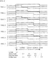
- FIG. 2 is a waveform diagram illustrating a method of pulse width modulation according to one embodiment of a method of driving a display of the present invention.
- FIG. 3 is a block diagram illustrating a driving circuit realizing a method of driving a display according to one embodiment of the present invention.
- FIG. 2 illustrates one example of the present invention for explaining a method of controlling a light emitting time, and explains the example of a pulse width modulation for realizing seven pixels configured to display colors using four levels.
- a refresh cycle T1 is divided into four levels to individually control red R, green G, and blue B through the pulse width modulation. That is, the refresh cycle T1 for illuminating the pixel may include a plurality of levels.
- the luminance of the pixel may be determined by color combination of the red R, green G, and blue B emitted during the light emitting time in the refresh cycle T1.
- the light emitted from the pixel 1 during the refresh cycle T1 is determined by combination of the colors corresponding to the red R of the 4th level L4, the blue B of the 1st level L1, and the green G of the 2nd level L2.
- red R has a second level L2
- blue B has a fourth level L4
- the light emitted from the pixel 2 during the refresh cycle T1 is determined by combination of the colors corresponding to the red R of the 2nd level L2, the blue B of the 4th level L4, and the green G of the 3rd level L3.
- red R has a first level L1
- blue B has a second level L2
- the light emitted from the pixel 3 during the refresh cycle T1 is determined by combination of the colors corresponding to the red R of the 1st level L1, the blue B of the 2nd level L2, and the green G of the 4th level L4.
- the red R, blue B, and green G are respectively illuminated during the times of the 3rd level L3, the 3rd level L3, and the 2nd level L2, the light emitted from the pixel 4 during the refresh cycle T1 is determined by combination of the colors corresponding to the red R of the 3rd level L3, the blue B of the 3rd level L3, and the green G of the 2nd level L2.
- the red R, blue B, and green G are respectively illuminated during the times of the 2nd level L2, the 2nd level L2, and the 3rd level L3, the light emitted from the pixel 5 during the refresh cycle T1 is determined by combination of the colors corresponding to the red R of the 2nd level L2, the blue B of the 2nd level L2, and the green G of the 3rd level L3.
- the light emitted from the pixel 6 during the refresh cycle T1 is determined by combination of the colors corresponding to the red R of the 3rd level L3, the blue B of the 4th level L4, and the green G of the 2nd level L2.
- the red R, blue B, and green G are respectively illuminated during the times of the 1st level L1, the 1st level L1, and the 2nd level L2, the light emitted from the pixel 7 during the refresh cycle T1 is determined by combination of the colors corresponding to the red R of the 1st level L1, the blue B of the 1st level L1, and the green G of the 2nd level L2.
- the drive circuit 510 applies the signal of the low level within the time corresponding to the minimum level, and thus, the light emitting time may be controlled. That is, in the embodiment shown in FIG. 2 , the drive circuit 510 may apply the signal of the first level L1 to the red R of the pixels 3 and 7, and may apply the signal of the low level to the blue B of the pixels 1 and 7, and may not apply any signal to the green G.
- the driving circuit 510 may apply the signal of the second level L2 to the red R of the pixels 2 and 5 and the blue B of the pixels 3 and 5, and may apply the signal of the low level to the green G of the pixels 1, 4, 6, and 7.
- the driving circuit 510 may apply the signal of the third level L3 to the red R of the pixels 4 and 6 and the blue B of the pixel 4, and may apply the signal of the low level to the green G of the pixels 2 and 5.
- the driving circuit 510 may apply the signal of the fourth level L4 to the red R of the pixel 1 and the blue B of the pixels 2 and 6, and may apply the signal of the low level to the green G of the pixel 3.
- the three colors may be controlled using one drive circuit 510 shown in FIG. 3A , or may be respectively controlled using three drive circuits 510 shown in FIG. 3B .
- the method of driving the seven pixels of the four levels is described, but the method may control 256 light emitting times of 256 gray scales for 256 pixels.
- the refresh time is divided into 256, and the drive circuit may on/off control each of the pixels at a refresh rate of 256 Hz.
- the method of driving the display of the light emitting diode uses the pulse width modulation, and the light emitting time of the lights of the three primary colors is individually increased or decreased, thereby controlling the luminance of each pixel. That is, the refresh cycle T1 for illuminating the red R, blue B, and green G is divided into a plurality of levels for forming colors, and the control signals of the pulse width modulation are applied to the pixels by the drive circuit 510 to illuminate each of the colors, and then, the colors of the pixels are turned off by the signal of the low level at the corresponding level.
- the times for illuminating the red R, blue B, and green G are controlled in each pixel, and desired color may be illuminated by the combination of the times for illuminating the red R, blue B, and green G.
- illumination time of each of three primary colors of light on each pixel is controlled, and thus, luminance change caused by current change in a conventional current control method may be prevented.
- the display may be operated at a current of the maximum efficiency, and thus, efficiency of the display may be maximized.
Landscapes
- Engineering & Computer Science (AREA)
- Physics & Mathematics (AREA)
- Computer Hardware Design (AREA)
- General Physics & Mathematics (AREA)
- Theoretical Computer Science (AREA)
- Control Of Indicators Other Than Cathode Ray Tubes (AREA)
- Led Devices (AREA)
- Control Of El Displays (AREA)
Applications Claiming Priority (2)
| Application Number | Priority Date | Filing Date | Title |
|---|---|---|---|
| KR1020150116386A KR101725193B1 (ko) | 2015-08-19 | 2015-08-19 | 디스플레이 구동 방법 |
| PCT/KR2016/009147 WO2017030406A1 (fr) | 2015-08-19 | 2016-08-19 | Procédé de pilotage d'affichage |
Publications (2)
| Publication Number | Publication Date |
|---|---|
| EP3340226A1 true EP3340226A1 (fr) | 2018-06-27 |
| EP3340226A4 EP3340226A4 (fr) | 2019-01-09 |
Family
ID=58051370
Family Applications (1)
| Application Number | Title | Priority Date | Filing Date |
|---|---|---|---|
| EP16837348.8A Withdrawn EP3340226A4 (fr) | 2015-08-19 | 2016-08-19 | Procédé de pilotage d'affichage |
Country Status (6)
| Country | Link |
|---|---|
| US (1) | US10460651B2 (fr) |
| EP (1) | EP3340226A4 (fr) |
| JP (1) | JP2018525685A (fr) |
| KR (1) | KR101725193B1 (fr) |
| CN (1) | CN107924661A (fr) |
| WO (1) | WO2017030406A1 (fr) |
Families Citing this family (5)
| Publication number | Priority date | Publication date | Assignee | Title |
|---|---|---|---|---|
| KR102692880B1 (ko) | 2016-12-21 | 2024-08-08 | 주식회사 엘엑스세미콘 | 디스플레이 장치의 클럭 복원 회로 |
| CN118231439A (zh) * | 2017-09-11 | 2024-06-21 | 维耶尔公司 | 微型led器件和阵列的维修技术 |
| CN113096586B (zh) * | 2019-12-20 | 2022-08-02 | 深圳蓝普科技有限公司 | 一种显示屏及其灰度调制方法、显示设备及存储介质 |
| KR102837109B1 (ko) * | 2020-05-21 | 2025-07-24 | 삼성디스플레이 주식회사 | 표시 장치 |
| CN112509524B (zh) * | 2020-11-18 | 2021-10-29 | 深圳市慧为智能科技股份有限公司 | 水墨屏快速刷新方法、装置、设备及计算机可读存储介质 |
Family Cites Families (17)
| Publication number | Priority date | Publication date | Assignee | Title |
|---|---|---|---|---|
| JP2000214825A (ja) * | 1999-01-20 | 2000-08-04 | Nec Corp | バックライト表示装置及び方法 |
| JP2003044016A (ja) * | 2001-08-02 | 2003-02-14 | Matsushita Electric Ind Co Ltd | 液晶表示装置及び液晶表示装置の駆動方法 |
| CN2600890Y (zh) * | 2003-03-07 | 2004-01-21 | 深圳市和而泰电子科技有限公司 | 多色彩动态显示装置 |
| US7817330B2 (en) * | 2003-11-01 | 2010-10-19 | Silicon Quest Kabushiki-Kaisha | Projection apparatus with adjustable light source |
| KR20050049913A (ko) | 2003-11-24 | 2005-05-27 | 주식회사 씨모텍 | 소형 기기의 발광다이오드 구동 회로 및 구동 방법 |
| JP2007078866A (ja) * | 2005-09-12 | 2007-03-29 | Sharp Corp | 空間光変調システム、その駆動方法及びプロジェクタ |
| KR100843690B1 (ko) * | 2006-04-24 | 2008-07-04 | 엘지디스플레이 주식회사 | 발광 소자 |
| US8044984B2 (en) * | 2008-03-27 | 2011-10-25 | Himax Technologies Limited | Methods for driving an OLED panel |
| KR100948057B1 (ko) * | 2009-08-18 | 2010-03-19 | 주식회사 대청마스터스 | 절전형 엘이디 전광판 시스템 |
| US8084775B2 (en) * | 2010-03-16 | 2011-12-27 | Bridgelux, Inc. | Light sources with serially connected LED segments including current blocking diodes |
| CN201657436U (zh) * | 2010-04-23 | 2010-11-24 | 北京朗波尔光电股份有限公司 | Led灯光控制装置 |
| US8962358B2 (en) * | 2011-03-17 | 2015-02-24 | Tsmc Solid State Lighting Ltd. | Double substrate multi-junction light emitting diode array structure |
| KR101169020B1 (ko) | 2011-04-01 | 2012-07-31 | 배가은 | 엘이디 전광판 |
| WO2013016346A1 (fr) * | 2011-07-25 | 2013-01-31 | Cree, Inc. | Diode électroluminescente émettant par la surface haute tension et faible courant |
| EP2658000B1 (fr) * | 2012-03-13 | 2018-05-02 | Panasonic Intellectual Property Management Co., Ltd. | Substrat, dispositif électroluminescent et dispositif d'éclairage |
| KR101490174B1 (ko) * | 2013-07-29 | 2015-02-05 | 광주과학기술원 | 다중 접합 구조를 가지는 발광 다이오드 및 이의 형성방법 |
| KR102364160B1 (ko) * | 2014-03-06 | 2022-02-21 | 서울반도체 주식회사 | Mjt led를 이용한 백라이트 모듈 및 이를 포함하는 백라이트 유닛 |
-
2015
- 2015-08-19 KR KR1020150116386A patent/KR101725193B1/ko active Active
-
2016
- 2016-08-19 EP EP16837348.8A patent/EP3340226A4/fr not_active Withdrawn
- 2016-08-19 CN CN201680047420.2A patent/CN107924661A/zh not_active Withdrawn
- 2016-08-19 WO PCT/KR2016/009147 patent/WO2017030406A1/fr not_active Ceased
- 2016-08-19 JP JP2018527707A patent/JP2018525685A/ja active Pending
-
2018
- 2018-02-19 US US15/899,113 patent/US10460651B2/en active Active
Also Published As
| Publication number | Publication date |
|---|---|
| KR20170021982A (ko) | 2017-03-02 |
| CN107924661A (zh) | 2018-04-17 |
| JP2018525685A (ja) | 2018-09-06 |
| WO2017030406A1 (fr) | 2017-02-23 |
| EP3340226A4 (fr) | 2019-01-09 |
| US20180174506A1 (en) | 2018-06-21 |
| KR101725193B1 (ko) | 2017-04-11 |
| US10460651B2 (en) | 2019-10-29 |
Similar Documents
| Publication | Publication Date | Title |
|---|---|---|
| US10460651B2 (en) | Method for driving display | |
| TWI455101B (zh) | 影像顯示裝置之驅動方法及影像顯示裝置組合之驅動方法 | |
| CN111028766B (zh) | 像素和显示装置 | |
| EP3866151A1 (fr) | Pixel, dispositif d'affichage comportant celui-ci et son procédé d'entraînement | |
| TWI522988B (zh) | 具多階驅動的電致發光裝置老化補償 | |
| EP2317496A1 (fr) | Dispositif d'affichage à del | |
| US20150054815A1 (en) | Driving method of organic el display device and organic el display device | |
| TW201308305A (zh) | 顯示裝置及用於產生圖像於其上的方法 | |
| WO2017107290A1 (fr) | Dispositif d'affichage à diodes électroluminescentes organiques (delo) et dispositif de pilotage de source | |
| CN113611246A (zh) | 微型发光二极管显示装置 | |
| JP2006285236A (ja) | 発光表示装置及びその駆動方法 | |
| JP2005197304A (ja) | 発光装置 | |
| TW200638318A (en) | Light emitting display device and method of driving the same | |
| CN111554240A (zh) | 显示装置的驱动方法及显示装置 | |
| CN102695331A (zh) | 背光装置、其控制方法以及显示装置 | |
| US11094250B2 (en) | Method and apparatus for an electroluminescent device | |
| TWI389083B (zh) | Pixel driver and display device | |
| US8513897B2 (en) | OLED display with a current stabilizing device and its driving method | |
| CN105719600A (zh) | 光产生装置和具有光产生装置的显示设备 | |
| CN104282267A (zh) | 主动矩阵有机发光二极管显示器及其像素控制方法 | |
| JP2006301450A (ja) | 発光装置、表示装置 | |
| KR102570515B1 (ko) | 타이밍 컨트롤러 및 이를 포함하는 표시장치 | |
| JP6974749B2 (ja) | 表示装置および表示装置の駆動方法 | |
| KR20250133743A (ko) | 발광 소자를 이용한 디스플레이 장치 및 그 구동 방법 | |
| KR101058104B1 (ko) | 적어도 2종의 유기 전계 발광 소자들을 구비하는 조명 장치및 이의 구동 방법 |
Legal Events
| Date | Code | Title | Description |
|---|---|---|---|
| PUAI | Public reference made under article 153(3) epc to a published international application that has entered the european phase |
Free format text: ORIGINAL CODE: 0009012 |
|
| 17P | Request for examination filed |
Effective date: 20180131 |
|
| AK | Designated contracting states |
Kind code of ref document: A1 Designated state(s): AL AT BE BG CH CY CZ DE DK EE ES FI FR GB GR HR HU IE IS IT LI LT LU LV MC MK MT NL NO PL PT RO RS SE SI SK SM TR |
|
| AX | Request for extension of the european patent |
Extension state: BA ME |
|
| DAV | Request for validation of the european patent (deleted) | ||
| DAX | Request for extension of the european patent (deleted) | ||
| A4 | Supplementary search report drawn up and despatched |
Effective date: 20181210 |
|
| RIC1 | Information provided on ipc code assigned before grant |
Ipc: H01L 33/00 20100101ALI20181204BHEP Ipc: G09G 3/3216 20160101ALI20181204BHEP Ipc: G09G 3/34 20060101AFI20181204BHEP |
|
| STAA | Information on the status of an ep patent application or granted ep patent |
Free format text: STATUS: THE APPLICATION IS DEEMED TO BE WITHDRAWN |
|
| 18D | Application deemed to be withdrawn |
Effective date: 20190718 |