EP3340321B1 - Prozessverfahren mit photokonverter aus verformbarem organischem silikonharz zur bond-verpackung einer led - Google Patents
Prozessverfahren mit photokonverter aus verformbarem organischem silikonharz zur bond-verpackung einer led Download PDFInfo
- Publication number
- EP3340321B1 EP3340321B1 EP15901621.1A EP15901621A EP3340321B1 EP 3340321 B1 EP3340321 B1 EP 3340321B1 EP 15901621 A EP15901621 A EP 15901621A EP 3340321 B1 EP3340321 B1 EP 3340321B1
- Authority
- EP
- European Patent Office
- Prior art keywords
- array
- led
- sheet
- photoconversion
- roll
- Prior art date
- Legal status (The legal status is an assumption and is not a legal conclusion. Google has not performed a legal analysis and makes no representation as to the accuracy of the status listed.)
- Active
Links
Images


Classifications
-
- H—ELECTRICITY
- H10—SEMICONDUCTOR DEVICES; ELECTRIC SOLID-STATE DEVICES NOT OTHERWISE PROVIDED FOR
- H10H—INORGANIC LIGHT-EMITTING SEMICONDUCTOR DEVICES HAVING POTENTIAL BARRIERS
- H10H20/00—Individual inorganic light-emitting semiconductor devices having potential barriers, e.g. light-emitting diodes [LED]
- H10H20/80—Constructional details
- H10H20/85—Packages
- H10H20/852—Encapsulations
- H10H20/853—Encapsulations characterised by their shape
-
- B—PERFORMING OPERATIONS; TRANSPORTING
- B29—WORKING OF PLASTICS; WORKING OF SUBSTANCES IN A PLASTIC STATE IN GENERAL
- B29C—SHAPING OR JOINING OF PLASTICS; SHAPING OF MATERIAL IN A PLASTIC STATE, NOT OTHERWISE PROVIDED FOR; AFTER-TREATMENT OF THE SHAPED PRODUCTS, e.g. REPAIRING
- B29C59/00—Surface shaping of articles, e.g. embossing; Apparatus therefor
- B29C59/02—Surface shaping of articles, e.g. embossing; Apparatus therefor by mechanical means, e.g. pressing
- B29C59/04—Surface shaping of articles, e.g. embossing; Apparatus therefor by mechanical means, e.g. pressing using rollers or endless belts
-
- H—ELECTRICITY
- H10—SEMICONDUCTOR DEVICES; ELECTRIC SOLID-STATE DEVICES NOT OTHERWISE PROVIDED FOR
- H10H—INORGANIC LIGHT-EMITTING SEMICONDUCTOR DEVICES HAVING POTENTIAL BARRIERS
- H10H20/00—Individual inorganic light-emitting semiconductor devices having potential barriers, e.g. light-emitting diodes [LED]
- H10H20/01—Manufacture or treatment
- H10H20/036—Manufacture or treatment of packages
- H10H20/0362—Manufacture or treatment of packages of encapsulations
-
- H—ELECTRICITY
- H10—SEMICONDUCTOR DEVICES; ELECTRIC SOLID-STATE DEVICES NOT OTHERWISE PROVIDED FOR
- H10H—INORGANIC LIGHT-EMITTING SEMICONDUCTOR DEVICES HAVING POTENTIAL BARRIERS
- H10H20/00—Individual inorganic light-emitting semiconductor devices having potential barriers, e.g. light-emitting diodes [LED]
- H10H20/80—Constructional details
- H10H20/81—Bodies
- H10H20/822—Materials of the light-emitting regions
-
- H—ELECTRICITY
- H10—SEMICONDUCTOR DEVICES; ELECTRIC SOLID-STATE DEVICES NOT OTHERWISE PROVIDED FOR
- H10H—INORGANIC LIGHT-EMITTING SEMICONDUCTOR DEVICES HAVING POTENTIAL BARRIERS
- H10H20/00—Individual inorganic light-emitting semiconductor devices having potential barriers, e.g. light-emitting diodes [LED]
- H10H20/80—Constructional details
- H10H20/85—Packages
- H10H20/851—Wavelength conversion means
- H10H20/8514—Wavelength conversion means characterised by their shape, e.g. plate or foil
-
- H—ELECTRICITY
- H10—SEMICONDUCTOR DEVICES; ELECTRIC SOLID-STATE DEVICES NOT OTHERWISE PROVIDED FOR
- H10H—INORGANIC LIGHT-EMITTING SEMICONDUCTOR DEVICES HAVING POTENTIAL BARRIERS
- H10H20/00—Individual inorganic light-emitting semiconductor devices having potential barriers, e.g. light-emitting diodes [LED]
- H10H20/80—Constructional details
- H10H20/85—Packages
- H10H20/852—Encapsulations
- H10H20/854—Encapsulations characterised by their material, e.g. epoxy or silicone resins
-
- H—ELECTRICITY
- H10—SEMICONDUCTOR DEVICES; ELECTRIC SOLID-STATE DEVICES NOT OTHERWISE PROVIDED FOR
- H10W—GENERIC PACKAGES, INTERCONNECTIONS, CONNECTORS OR OTHER CONSTRUCTIONAL DETAILS OF DEVICES COVERED BY CLASS H10
- H10W90/00—Package configurations
-
- H—ELECTRICITY
- H10—SEMICONDUCTOR DEVICES; ELECTRIC SOLID-STATE DEVICES NOT OTHERWISE PROVIDED FOR
- H10H—INORGANIC LIGHT-EMITTING SEMICONDUCTOR DEVICES HAVING POTENTIAL BARRIERS
- H10H20/00—Individual inorganic light-emitting semiconductor devices having potential barriers, e.g. light-emitting diodes [LED]
- H10H20/01—Manufacture or treatment
- H10H20/036—Manufacture or treatment of packages
- H10H20/0361—Manufacture or treatment of packages of wavelength conversion means
Definitions
- the present invention relates to the technical field of LED packaging using a photoconverter, and in particular, to a process for bond-packaging an LED using a special-shaped organic silicone resin photoconverter.
- LEDs are known as the most promising new generation of green light sources in the 21 st century.
- the theoretical service life of the LED can be over 100,000 hours.
- the LED prematurely encounters luminous decay or loss of luminous efficacy, thus hindering development of the LED to be a novel energy-saving light source.
- many scholars in the field have carried out related researches, and have proposed some improvement measures to enhance luminous efficacy and actual service life of the LED. For example, flip-chip LED packaging is developed in recent years.
- this flip-chip manner has such advantages as high luminous efficacy, high reliability, and easy integration.
- This manner also greatly saves packaging materials. For example, materials such as a gold wire, die bonding glue, and a support that are used in the conventional LED upright packaging are no longer needed. Further, this manner greatly simplifies a packaging process. For example, die bonding, wire soldering, and even light splitting in the conventional LED upright packaging are no longer needed. In this way, the LED flip-chip packaging is increasingly widely applied.
- the existing flip-chip LED packaging technologies mostly bond a photoconverter made of an organic silicone resin to a flip chip LED by using a casting process, a screen printing process, an upper and lower flat plate molding process, a single roller pressing process, and the like.
- These processes and matched packaging equipment cannot desirably solve flaws such as pores and unequal thickness of the photoconverter made of the organic silicone resin, thus causing a low yield of the LEDs packaged by using a photoconverter.
- due to low production efficiency the high product costs cannot be reduced.
- Chinese patent application NO. 201010204860.9 discloses a "flip-chip LED packaging method", which includes steps of: (a) coating a surface of an LED chip with a photoconverter through screen printing, and baking the photoconverter to cure the photoconverter; (b) fixing the LED chip on a chip substrate, such that electrodes of the LED chip and electrodes of the chip substrate are bonded; (c) fixing the LED chip and the chip substrate to the bottom of a reflector cup on a support; (d) separately connecting positive and negative electrodes of the fixed chip substrate to positive and negative electrodes of the support by using wires; (e) placing a sealing mold or lens cover on the support on which the LED chip and the chip substrate are fixed, and filling the sealing mold or lens cover with silica gel; and (f) baking a whole structure to cure it.
- This method uses the screen printing process to enhance uniformity of coating thickness of the photoconverter and enhance distribution uniformity of fluorescent powder particles, so as to improve the yield.
- the surface of the LED chip is coated with the photoconvertermade of the organic silicone resin through a screen printing process, due to thermal overstress in a subsequent baking and curing procedure, pores still occur in part of the photoconverter coating and the coated surface of the LED chip, thus forming sags and crests.
- Cida 201310270747.4 discloses an "LED coated with photoconverter layer, manufacturing method for same, and LED device".
- This solution includes: an LED configuration stage, in which an LED is configured on a surface of a support chip in a through-thickness direction; a layer configuration stage, in which a photoconverter layer is configured on a surface of the support chip in the through-thickness direction in the same manner as LED configuration, the photoconverter layer being formed by active energy ray cured resin which is cured by irradiation with an active energy ray and a fluorescent resin composition of the photoconverter; a curing stage, in which the photoconverter layer is irradiated with an active energy ray to cure the photoconverter layer; a cutting stage, in which the photoconverter layer is cut corresponding to the LED, to obtain an LED coated with the photoconverter layer; and an LED separation stage, in which the LED coated with the photoconverter layer is separated from the support chip after the cutting process.
- This method aims to offer a solution to uniform configuration of photoconverters around the LED to avoid damage, thus obtaining an LED coated with a photoconverter layer, and an LED device having the LED coated with the photoconverter layer.
- Japanese patent application NO. 201380027218.X discloses a "resin sheet laminate, and manufacturing method for semiconductor light-emitting elements using same".
- the resin sheet laminate is formed by disposing a fluorophor-containing resin layer on a substrate, where the fluorophor-containing resin layer has multiple regions, the substrate has a lengthwise direction and a transverse direction, and the multiple regions are arranged along the lengthwise direction repeatedly to form columns.
- this solution aims to enhance uniformity of color and brightness of semiconductor light-emitting elements to which the fluorophor-containing resin layer is attached, and make it easy to manufacture and free to design the elements.
- the used fluorescent resin sheet is a cured fluorescent resin sheet, and therefore, possible residual pores, sags and crests, or other flaws produced during processing cannot be effectively eliminated.
- a pressure is exerted by a pressurizing tool from a side of the semiconductor light-emitting elements, which may damage the semiconductor light-emitting elements.
- the bonding stage using an adhesive in the fluorophor-containing resin layer it is difficult to eliminate residuals from the semiconductor light-emitting elements after bonding, and pores easily occur in the bonding procedure, thus reducing the yield; in addition, existence of the bonding layer reduces light emission efficiency of the LED elements.
- the substrate under the fluorescent resin sheet bonded to the light emitting surface of the semiconductor light-emitting elements is not removed, which directly affects luminous efficacy of the semiconductor light-emitting elements.
- the multiple regions of the fluorophor-containing resin layer are arranged in the lengthwise direction repeatedly to form columns, but actually it is complex to arrange the multiple regions of the fluorophor-containing resin layer in such a manner, thus affecting the packaging efficiency of the whole elements.
- An error in arrangement positions of the multiple regions directly affects the precision of subsequent bonding with the light-emitting elements. If the multiple regions cannot be rendered uniform in size and thickness, a severe problem of product inconsistency may emerge.
- U.S. Patent Application Publication No. US20130143339 discloses a method for uniform application of a phosphor powder binder onto a LED chip to form broad-area lighting systems.
- a phosphor material is adhered onto a substrate on a surface of a first roll by applying an electrostatic electric field.
- the phosphor material is transferred to a second substrate by a dispenser and bonded to the LED chip.
- the phosphor material is fixed on the surface of the LED chip by curing of the binder.
- This method has the following disadvantages: 1) the transfer of the phosphor binder material to the surface of the chip by the dispenser would inevitably generate bubbles, which tends to cause a low yield rate; 2) in this method, during the curing process of the binder, holding pressure is provided by the tension of the thin film material, which would inevitably cause deviations in the product size and difficulty to control the precision; and 3) the procedure in the whole forming process is relatively cumbersome, involving more control systems, and the production efficiency of the packaged LEDs is not high.
- An objective of the present invention is to overcome the defects in the prior art and provide a process for bond-packaging an LED using a special-shaped organic silicone resin photoconverter.
- the present invention has a significant advantage of bond-packaging the LED by continuous rolling, can meet a condition requirement of bond-packaging an LED using a special-shaped organic silicone resin photoconverter, and enhance the production efficiency and yield of LED packages in industrialized batch production.
- a process for bond-packaging an LED using a special-shaped organic silicone resin photoconverter includes the following continuous process flow: roll-molding of a refined photoconversion sheet, roll-shaping of a photoconversion sheet array, sheet melting for the photoconversion sheet array, preparation of a flip chip LED array sheet, forming of LED package elements by roll-bonding, curing of the LED package elements, and cutting of the LED package elements, including the following basic steps:
- An implementation principle of the present invention is as follows: To better solve the major problems in the existing LED packaging process, the present invention subtly designs a novel process for bond-packaging an LED using a special-shaped organic silicone resin photoconverter.
- a principle of bond-packaging by rolling of the present invention is as follows: First, a roller is used to roll a semi-cured photoconversion sheet to produce a flow in sags and crests in the sheet, so as to eliminate possible residual pores, sags and crests, or other flaws produced during processing in the semi-cured photoconversion sheet, thereby obtaining a flat refined photoconversion sheet without pores and having a uniform thickness.
- the rolled semi-cured photoconversion sheet is deformable during processing, to form a photoconverter light emitting surface layer with a required optimal shape, such as an arc, a hemisphere, or a rectangle.
- the material of the second outer protective film is meltable organic silicon photosensitive resin containing a photoconversion material, and therefore the second outer protective film and the semi-cured photoconversion sheet can be effectively fused and integrated by means of illumination, thus achieving tight bonding to flip chip LEDs.
- the present invention provides a continuous process flow, which can meet processing conditions of batch production of LED package elements and achieve completely consistent specifications and dimensions. In this way, the production efficiency of the LED package elements is enhanced, brightness and color uniformity of finished LED package elements is improved, and the yield is greatly improved.
- Embodiment 1 Referring to FIG. 1 and FIG. 2 , the present invention provides a process for bond-packaging an LED using a special-shaped organic silicone resin photoconverter, which includes the following continuous process flow: roll-molding of a refined photoconversion sheet, roll-shaping of a photoconversion sheet array, sheet melting for the photoconversion sheet array, preparation of a flip chip LED array sheet, forming of LED package elements by roll-bonding, curing of the LED package elements, and cutting of the LED package elements.
- the process specifically includes the following steps:
- the present invention is applicable to production and processing of a photoelectric device or an electronic device of a structure similar to that of a flip chip LED.
- any existing organic silicone resin having high light transmittance and desirable temperature resistance may be selected to be used in the process of the present invention.
- the present invention preferably uses methyl vinyl organic silicone resin.
- Existing quantum dotfluorophorand fluorescent powder can both be selected to be used in the process of the present invention.
- mixed slurry used in the present invention does not need to contain an adhesive.
- the mixed slurry used in the present invention may contain an adhesive.
- the roll-molding of a refined photoconversion sheet in step 1 refers to rolling a first outer protective film, a semi-cured photoconversion material, and a second outer protective film by using one or more sets of smooth-surface roll-laminating apparatuses, where rolling is performed sequentially by using one or more sets of smooth-surface double-roller roll-laminating apparatuses that are disposed face-to-face and aligned with each other and/or a rolling apparatus formed by a smooth-surface single-wheeled roller and a smooth-surface planar conveyor, to obtain a refined photoconversion sheet.
- the roll-molding of a refined photoconversion sheet in step 1 refers to rolling a first outer protective film, a semi-cured photoconversion material, and a second outer protective film by using one or more sets of smooth-surface roll-laminating apparatuses, where rolling is performed sequentially by using one or more sets of smooth-surface double-roller roll-laminating apparatuses that are disposed face-to-face and aligne
- FIG. 3A shows step 1 of rolling a first outer protective film (8-3), a semi-cured photoconversion membrane (8-1), and an second outer protective film(8-4) by using one set of smooth-surface roll-laminating apparatuses, to obtain a refined photoconversion sheet (8-6);
- FIG. 3B shows step 1 of rolling a first outer protective film (8-3), semi-cured photoconversion slurry (8-2), and a second outer protective film(8-4) by using one set of smooth-surface roll-laminating apparatuses, to obtain a refined photoconversion sheet (8-6);
- FIG. 3A shows step 1 of rolling a first outer protective film (8-3), a semi-cured photoconversion membrane (8-1), and an second outer protective film(8-4) by using one set of smooth-surface roll-laminating apparatuses, to obtain a refined photoconversion sheet (8-6);
- FIG. 3B shows step 1 of rolling a first outer protective film (8-3), semi-cured photoconversion slurry (8-2), and a second outer protective film(8
- 3C shows step 1 of rolling a first outer protective film (8-3), semi-cured photoconversion slurry (8-2), and an second outer protective film(8-4) by using two sets of smooth-surface roll-laminating apparatuses, to obtain a refined photoconversion sheet (8-6).
- the temperature of the roll-molding of a refined photoconversion sheet in step 1 ranges from 50°C to 120°C.An optimal temperature of the roll-molding ranges from 80°C to 100°C.
- the thickness of the refined photoconversion sheet in step 1 is no more than800 ⁇ m.
- An optimal thickness of the refined photoconversion sheet ranges from 150 ⁇ m to 250 ⁇ m.
- a material of the semi-cured photoconversion sheet in step 1 is a semi-cured organic silicone resin fluorescent powder membrane or a semi-cured organic silicone resin quantum dot fluorophormembrane.
- a material of the first outer protective film in step 1 is polyester, polyolefin, or polyether.
- the photoconversion material in the second outer protective film in step 1 and the photoconversion material in the semi-cured photoconversion sheet are identical materials with identical contents.
- the material of the second outer protective film further includes an adhesive.
- the first rolling device with a protrusion array is a first single-wheeled roller with a protrusion array or a first planar conveyor with a protrusion array
- the second rolling device with a recess array is a second single-wheeled roller with a recess array or a second planar conveyor with a recess array
- at least one of the first rolling device and the second rolling device is a single-wheeled roller.
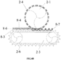
- FIG. 4A shows step 2 of performing heating and roll-shaping on the refined photoconversion sheet(8-6) with the first outer protective film (8-3) and the second outer protective film (8-4) by using a first single-wheeled roller (2-1) with a protrusion array and a second single-wheeled roller (2-2) with a recess array that are disposed face-to-face and aligned with each other, to obtain a photoconversion sheet array formed by individual photoconversion sheets (8-7) with recesses; and FIG.
- step 2 shows step 2 of performing heating and roll-shaping on the refined photoconversion sheet(8-6) with the first outer protective film (8-3) and the second outer protective film (8-4) by using a first single-wheeled roller 1 (2-1) with a protrusion array and a second planar conveyor (2-3) with a recess array that are disposed face-to-face and aligned with each other, to obtain a photoconversion sheet array formed by individual photoconversion sheets (8-7) with recesses.
- each individual photoconversion sheet with recesses in step 2 is an arc, a hemisphere, or a rectangle.
- the length, width, and height of a recess are 1.01 to 1.05 times of those of a flip chip LED.
- the length, width, and height of the recess are 1.02 times of those of the flip chip LED .
- the temperature of the roll-shaping of a photoconversion sheet array in step 2 ranges from 50°C to 120°C.An optimal temperature of the roll-shaping ranges from 80°C to 100°C.
- the sheet melting in step 3 refers to: melting the second outer protective film by means of light irradiation and integrating the melted sheet with the semi-cured photoconversion sheet in step 1.
- FIG. 5 shows that in step 3, before sheet melting, the photoconversion sheet array formed by individual photoconversion sheets (8-7) with recesses passes through a sheet-melting apparatus 3, and the second outer protective film (8-4) of the photoconversion sheet array is illuminated by light and then is integrated with the semi-cured photoconversion sheet, to obtain a sheet-melted photoconversion sheet array formed by individual photoconversion sheets (8-8) with recesses.
- the carrier film in the flip chip LED array sheet in step 4 is a stretchable carrier film, and a material of the stretchable carrier film is one of heat-resistant polyester, polydimethylsiloxane, and polyvinyl chloride.
- Step 5 of performing roll-bonding on the sheet-melted photoconversion sheet array in step 3 and the flip chip LED array sheet in step 4 by using a third rolling device with a smooth surface and a fourth rolling device with a recess array, the photoconversion sheet array and the flip chip LED array sheet facing each other and being aligned with each other refers to: arranging the photoconversion sheet array on a fourth single-wheeled roller with a recess array or a fourth planar conveyor with a recess array, arranging the flip chip LED array sheet on a third single-wheeled roller with a smooth roll surface or a third planar conveyor with a smooth plane, and then performing roll-bonding, such that the flip chip LEDs in the flip chip LED array are bonded to and embedded in the recesses on the photoconversion sheets of the sheet-melted photoconversion sheet array, to obtain the LED package elements.
- the third rolling device with a smooth surface is the third single-wheeled roller with a smooth roll surface or the third planar conveyor with a smooth plane
- the fourth rolling device with a recess array is the fourth single-wheeled roller with a recess array or the fourth planar conveyor with a recess array
- at least one of the device arranged with the photoconversion sheet array and the device arranged with the flip chip LED array sheet is a single-wheeled roller.
- FIG. 6 shows step 5 of performing roll-bonding on the photoconversion sheet array formed by individual photoconversion sheets (8-8) after sheet melting and the flip chip LED array sheet by using the third single-wheeled roller (4-1) with a smooth surface and the fourth single-wheeled roller (4-2) with a recess array, the photoconversion sheet array and the flip chip LED array sheet facing each other and being aligned with each other, to obtain LED package elements (8-9).
- the temperature of the forming of LED package elements by roll-bonding in step 5 ranges from 50°C to 120°C.
- An optimal temperature of the roll-bonding in step 5 ranges from 80°C to 100°C.
- the photocuring in step 6 is curing with an active energy ray; and the curing temperature of the heatcuring ranges from 140°C to 180°C, and curing duration is greater than or equal to 1h.
- An optimal curing temperature ranges from 150°C to 160°C, and optimal curing duration is 2h.
- the width of the slit in step 7 is within20 ⁇ m.
- An optimal width of the slit is 15 ⁇ m.
- Step 7 of cutting of the cured LED package elements refers to: performing roll-cutting on the cured LED package elements by using a fifth rolling device with an array cutter and a sixth rolling device with a smooth surface in a face-to-face alignment manner, to obtain finished LED package elements having slits for splitting the finished product into individual LED package elements.
- the fifth rolling device with an array cutter is a fifth single-wheeled roller with an array cutter or a fifth planar conveyor with an array cutter
- the sixth rolling device with a smooth surface is a sixth single-wheeled roller with a smooth surface or a sixth planar conveyor with a smooth surface
- at least one of the fifth rolling device with an array cutter and the sixth rolling device with a smooth surface is a single-wheeled roller
- the array cutter being a cutter having an array of rectangular grids. Dimensions of the rectangular grid are the same as those of finished individual LED package elements.
- a stretcher may be used to stretch the stretchable carrier film of the finished LED package elements of the present invention, such that the finished LED package elements are split along the slits after being stretched, to obtain finished individual LED package elements, as shown in FIG. 7A and FIG. 7B .
- Each finished individual LED package element manufactured according to the present invention may be an arc-shaped LED package element, a hemispheric LED package element, or a rectangular LED package element, as shown in FIGs. 8A , 8B and 8C .
- the process for bond-packaging an LED using a special-shaped organic silicone resin photoconverter provided by the present invention is widely applicable to a packaging process of bonding an organic silicone resin photoconverter to LEDs of different power.
- Embodiment 2 provides an equipment system applied to a process for bond-packaging an LED using a special-shaped organic silicone resin photoconverter, which includes: a smooth-surface roll-laminating apparatus used for refining a photoconversion sheet; a roll-shaping apparatus used for performing heating and roll-shaping on the refined photoconversion sheet; a sheet-melting apparatus used for performing sheet melting on the roll-shaped refined photoconversion sheet; and a roll-bonding apparatus used for performing roll-bonding on the sheet-melted refined photoconversion sheet and a flip chip LED array with a carrier film, the refined photoconversion sheet and the flip chip LED array facing each other and being aligned with each other.
- a smooth-surface roll-laminating apparatus used for refining a photoconversion sheet
- a roll-shaping apparatus used for performing heating and roll-shaping on the refined photoconversion sheet
- a sheet-melting apparatus used for performing sheet melting on the roll-shaped refined photoconversion sheet
- the roll-laminating apparatus, the roll-shaping apparatus, the sheet-melting apparatus, and the roll-bonding apparatus are arranged sequentially to form cooperatively linked process equipment.
- the roll-laminating apparatus includes one or more sets of smooth-surface rolling components A and smooth-surface rolling components B that perform rolling face-to-face in alignment with each other.
- the roll-shaping apparatus includes a first rolling device with a protrusion array and a second rolling device with a recess array that perform rolling face-to-face in alignment with each other.
- the roll-bonding apparatus includes a third rolling device with a smooth surface and a fourth rolling device with a recess array that perform rolling face-to-face in alignment with each other.
- the smooth-surface rolling component A is a smooth-surface single-wheeled roller A or a smooth-surface planar conveyor A
- the smooth-surface rolling component B is a smooth-surface single-wheeled roller B or a smooth-surface planar conveyor B
- at least one of the smooth-surface rolling component A and the smooth-surface rolling component B is a single-wheeled roller.
- FIG. 3A shows that the smooth-surface rolling device includes a smooth-surface single-wheeled roller A1 (1-1) and a smooth-surface single-wheeled roller B1 (1-2) that perform rolling face-to-face in alignment with each other;
- FIG. 3B shows that the roll-laminating apparatus includes a smooth-surface single-wheeled roller A1 (1-1) and a smooth-surface single-wheeled roller B1 (1-2) that perform rolling face-to-face in alignment with each other; and FIG.
- the roll-laminating apparatus includes two sets of smooth-surface rolling components A and smooth-surface rolling components B, specifically including a smooth-surface single-wheeled roller A1 (1-1) and a smooth-surface single-wheeled roller B1 (1-2) that perform rolling face-to-face in alignment with each other, and a smooth-surface single-wheeled roller A2 (1-3) and a smooth-surface single-wheeled roller B2 (1-4) that perform rolling face-to-face in alignment with each other.
- the one or more sets of smooth-surface roll-laminating apparatuses are used to roll a first outer protective film (8-3), a semi-cured photoconversion membrane (8-1) or semi-cured photoconversion slurry (8-2), and an second outer protective film(8-4), to obtain a refined photoconversion sheet (8-6).
- the first rolling device with a protrusion array is a first single-wheeled roller with a protrusion array or a first planar conveyor with a protrusion array
- the second rolling device with a recess array is a second single-wheeled roller with a recess array or a second planar conveyor with a recess array
- at least one of the first rolling device and the second rolling device is a single-wheeled roller.
- FIG. 4A shows that the roll-shaping apparatus includes a first single-wheeled roller (2-1) with a protrusion array and a second single-wheeled roller (2-2) with a recess array that are disposed face to face and aligned with each other; and
- FIG. 4B shows that the roll-shaping apparatus includes a first single-wheeled roller (2-1) with a protrusion array and a second planar conveyor (2-3) with a recess array that are disposed face to face and aligned with each other.
- the roll-shaping apparatus is used to perform heating and roll-shaping on the refined photoconversion sheet (8-6) with the first outer protective film (8-3) and the second outer protective film (8-4), to obtain a photoconversion sheet array formed by individual photoconversion sheets (8-7) with recesses.
- the sheet-melting apparatus is a light irradiation apparatus.
- FIG. 5 shows that, before sheet melting, the photoconversion sheet array formed by individual photoconversion sheets (8-7) with recesses passes through the sheet-melting apparatus 3, and the second outer protective film (8-4) of the photoconversion sheet array is radiated by light and then is integrated with the semi-cured photoconversion sheet, to obtain a sheet-meltedphotoconversion sheet array formed by individual photoconversion sheets (8-8) with recesses.
- the third rolling device with a smooth surface is a third single-wheeled roller with a smooth roll surface or a third planar conveyor with a smooth plane
- the fourth rolling device with a recess array is a fourth single-wheeled roller with a recess array or a fourth planar conveyor with a recess array
- at least one of the device arranged with the photoconversion sheet array and the device arranged with a flip chip LED array sheet is a single-wheeled roller.
- the roll-bonding apparatus includes a third single-wheeled roller (4-1) with a smooth surface and a fourth single-wheeled roller (4-2) with a recess array that perform rolling face-to-face in alignment with each other.
- the third single-wheeled roller (4-1) with a smooth surface and the fourth single-wheeled roller (4-2) with a recess array are used to perform roll-bonding on the sheet-meltedphotoconversion sheet array formed by individual photoconversion sheets (8-8) and the flip chip LED array sheet, the photoconversion sheet array and the flip chip LED array sheet facing each other and being aligned with each other, to obtain LED package elements (8-9).
- the roll-laminating apparatus is provided with a displacement adjusting device for adjusting a distance between the smooth-surface rolling component A and the smooth-surface rolling component B.
- the roll-shaping apparatus is provided with a displacement adjusting device for adjusting a distance between the first rolling device and the second rolling device.
- the roll-bonding apparatus is provided with a displacement adjusting device for adjusting a distance between the third rolling device and the fourth rolling device.
- Either of the smooth-surface rolling component A and the smooth-surface rolling component B in the roll-laminating apparatus is a single-wheeled roller, and a radial run-out distance of the roller is less than or equal to 2 ⁇ m.
- Either of the first rolling device with a protrusion array and the second rolling device with a recess array in the roll-shaping apparatus is a single-wheeled roller, and a radial run-out distance of the roller is less than or equal to 2 ⁇ m.
- Either of the third rolling device with a smooth surface and the fourth rolling device with a recess array in the roll-bonding apparatus is a single-wheeled roller, and a radial run-out distance of the roller is less than or equal to 2 ⁇ m.
- the recess arrays have the same recess shape, where the recess shape is an arc, a hemisphere, or a rectangle.
- the shape of a protrusion in the protrusion array is a rectangle, and the length, width, and height of the protrusion are 1.01 to 1.05 times of those of a flip chip LED.
- the equipment system further includes a curing apparatus for curing LED package elements, where the curing apparatus is process equipment located at a rear end of the roll-bonding apparatus.
- the curing apparatus is a tunnel-type temperature control apparatus or a tunnel-type illuminating apparatus.
- the tunnel-type temperature control apparatus includes a heating component, a temperature control component and a conveyor belt passage.
- the tunnel-type illuminating apparatus includes an illuminating component, an illumination intensity control component and a conveyor belt passage.
- the equipment system further includes a cutting apparatus for cutting cured LED package elements, where the cutting apparatus is process equipment disposed at a rear end of the curing apparatus.
- the cutting apparatus is a roll-cutting apparatus, where the roll-cutting apparatus includes a rolling component C with an array cutter and a rolling component D with a smooth surface that are disposed face-to-face and aligned with each other.
- the rolling component C with an array cutter in the roll-cutting apparatus is a single-wheeled roller C with an array cutter or a planar conveyor C with an array cutter.
- the rolling component D with a smooth surface is a single-wheeled roller D with a smooth surface or a planar conveyor D with a smooth surface.
- At least one of the rolling component C with an array cutter and the rolling component D with a smooth surface is a single-wheeled roller.
- the array cutter is a cutter having an array of rectangular grids. Dimensions of the rectangular grid are the same as those of finished individual LED package elements.
- the roll-cutting apparatus is provided with a displacement adjusting device for adjusting a distance between the rolling component C with an array cutter and the rolling component D with a smooth surface.
- a displacement adjusting device for adjusting a distance between the rolling component C with an array cutter and the rolling component D with a smooth surface.
- Either of the rolling component C with an array cutter and the rolling component D with a smooth surface is a single-wheeled roller, and a radial run-out distance of the roller is less than or equal to 2 ⁇ m.
- the equipment system further includes a flip chip LED array forming apparatus for forming a flip chip LED array.
- the LED flip chip array forming apparatus is process equipment disposed at a front end of the roll-bonding apparatus.
- the LED flip chip array forming apparatus includes a manipulator for grabbing and placing a flip chip LED, and a planar conveying component having an accurate displacement positioning function.
- the roll-laminating apparatus, the roll-shaping apparatus, the sheet-melting apparatus, the chip array forming apparatus, the roll-bonding apparatus, the curing apparatus, and the cutting apparatus in the equipment system are sequentially and cooperatively linked, to form flow-type continuous process equipment.
- the present invention gains a satisfactory trial result after repeated test and verification.
Landscapes
- Engineering & Computer Science (AREA)
- Mechanical Engineering (AREA)
- Led Device Packages (AREA)
- Microelectronics & Electronic Packaging (AREA)
Claims (20)
- Verfahren zur Bond-Kapselung einer LED unter Verwendung eines speziell geformten Photokonverters aus organischem Siliconharz, mit dem folgenden kontinuierlichen Verfahrensablauf:
Walzpressen einer verfeinerten Photokonversionsschicht, Walzformen eines Photokonversionsschicht-Arrays, Schichtschmelzen bei dem Photokonversionsschicht-Array, Herstellen einer Schicht aus einem Flip-Chip-LED-Array, Bilden von LED-Paketelementen durch Walzbonden, Härten der LED-Paketelemente und Schneiden der LED-Paketelemente, mit den folgenden grundlegenden Schritten:Schritt 1: Walzpressen einer verfeinerten Photokonversionsschicht (8-6): Unter Erwärmung im Vakuum wird eine erste äußere Schutzfolie (8-3), ein halbgehärtetes Photokonversionsmaterial und eine zweite äußere Schutzfolie (8-4) unter Verwendung eines oder mehrerer Sätze von Walzlaminiervorrichtungen mit glatter Oberfläche gewalzt, um eine verfeinerte Photokonversionsschicht (8-6) zu erhalten, die durch eine erste äußere Schutzfolie (8-3), eine halbgehärtete Photokonversionsschicht (8-5) und eine zweite äußere Schutzfolie (8-4) gebildet wird, wobei es sich bei dem halbgehärteten Photokonversionsmaterial um eine halbgehärtete Photokonversionsmembran (8-1) oder eine halbgehärtete Photokonversionsaufschlämmung (8-2) handelt, und wobei es sich bei dem Material der zweiten äußeren Schutzfolie (8-4) um ein schmelzbares lichtempfindliches organisches Siliconharz handelt, das mindestens ein Photokonversionsmaterial enthält;Schritt 2: Walzformen eines Photokonversionsschicht-Arrays: Im Vakuum wird das Erwärmen und Walzformen an der verfeinerten Photokonversionsschicht (8-6) mit den äußeren Schutzfolien unter Verwendung einer ersten Walzvorrichtung mit einem Array von Vorsprüngen und einer zweiten Walzvorrichtung mit einem Array von Aussparungen durchgeführt, die einander gegenüberliegen und aufeinander ausgerichtet sind, um ein Photokonversionsschicht-Array zu erhalten, das durch einzelne Photokonversionsschichten (8-7) mit Aussparungen gebildet wird, wobei sich die Aussparungen auf einer Seite nahe bei der zweiten äußeren Schutzfolie (8-4) befinden, und wobei die Form der einzelnen Photokonversionsschichten (8-7) mit Aussparungen eine spezielle Form ist;Schritt 3: Schichtschmelzen bei dem Photokonversionsschicht-Array: unter Beleuchtung im Vakuum wird die zweite äußere Schutzfolie (8-4) des Photokonversionsschicht-Arrays von Schritt 2 geschmolzen, um ein flächig geschmolzenes Photokonversionsschicht-Array zu erhalten;Schritt 4: Herstellen einer Schicht aus einem Flip-Chip-LED-Array: Beschaffen einer Schicht aus einem Flip-Chip-LED-Array, wobei die Flip-Chip-LEDs (4-4) in der Schicht aus einem Flip-Chip-LED-Array in einem Array auf einer Trägerfolie (4-5) angeordnet sind, wobei die Flip-Chip-LED (4-4) einen einzelnen LED-Flip-Chip oder eine Flip-Chip-LED-Baugruppe bezeichnet, und wobei sich die Flip-Chip-LED-Baugruppe aus zwei oder mehr einzelnen Flip-Chip-LEDs zusammensetzt;Schritt 5: Bilden von LED-Paketelementen durch Walzbonden: Unter Erwärmung im Vakuum wird das Walzbonden an dem flächig geschmolzenen Photokonversionsschicht-Array von Schritt 3 und der Schicht aus einem Flip-Chip-LED-Array von Schritt 4 unter Verwendung einer dritten Walzvorrichtung mit glatter Oberfläche und einer vierten Walzvorrichtung mit einem Array von Aussparungen durchgeführt, wobei das Photokonversionsschicht-Array und die Schicht aus einem Flip-Chip-LED-Array einander gegenüberliegen und aufeinander ausgerichtet sind, sodass die Flip-Chip-LEDs (4-4) in der Schicht aus einem Flip-Chip-LED-Array an die Aussparungen auf den einzelnen Photokonversionsschichten (8-8) des flächig geschmolzenen Photokonversionsschicht-Arrays gebondet und darin eingebettet sind, um LED-Paketelemente (8-9) zu erhalten, wobei die Form und die Abmessungen der Aussparungen des Arrays von Aussparungen der vierten Walzvorrichtung mit denen des Arrays von Aussparungen der zweiten Walzvorrichtung identisch sind;Schritt 6: Härten der LED-Paketelemente: Mittels Wärmehärtung und/oder Photohärtung werden die LED-Paketelemente (8-9) von Schritt 5 unter Verwendung einer Härtungsvorrichtung (5) gehärtet, um gehärtete LED-Paketelemente zu erhalten; undSchritt 7: Schneiden der LED-Paketelemente: Entfernen der ersten äußeren Schutzfolie (8-3) von den gehärteten LED-Paketelementen von Schritt 6 und Schneiden der gehärteten LED-Paketelemente, um fertige LED-Paketelemente zu bilden, die Schlitze zum Zerteilen des fertigen Produkts in einzelne LED-Paketelemente aufweisen. - Verfahren zur Bond-Kapselung einer LED unter Verwendung eines speziell geformten Photokonverters aus organischem Siliconharz nach Anspruch 1, wobei bei dem Walzpressen einer verfeinerten Photokonversionsschicht gemäß Schritt 1 das Walzen einer ersten äußeren Schutzfolie (8-3), eines halbgehärteten Photokonversionsmaterials und einer zweiten äußeren Schutzfolie (8-4) unter Verwendung eines oder mehrerer Sätze von Walzlaminiervorrichtungen mit glatter Oberfläche Folgendes bezeichnet: Sequentielle Durchführung eines Walzvorgangs unter Verwendung eines oder mehrerer Sätze von Walzlaminiervorrichtungen mit zwei Walzen mit glatter Oberfläche, die einander gegenüberliegen und aufeinander ausgerichtet sind, und/oder einer Walzvorrichtung in Form einer Einzelradwalze mit glatter Oberfläche und einer ebenen Fördereinrichtung mit glatter Oberfläche, um die verfeinerte Photokonversionsschicht (8-6) zu erhalten.
- Verfahren zur Bond-Kapselung einer LED unter Verwendung eines speziell geformten Photokonverters aus organischem Siliconharz nach Anspruch 2, wobei die Temperatur beim Walzpressen einer verfeinerten Photokonversionsschicht in Schritt 1 im Bereich von 50°C bis 120°C liegt.
- Verfahren zur Bond-Kapselung einer LED unter Verwendung eines speziell geformten Photokonverters aus organischem Siliconharz nach Anspruch 3, wobei die Dicke der verfeinerten Photokonversionsschicht in Schritt 1 nicht mehr als 800 µm beträgt.
- Verfahren zur Bond-Kapselung einer LED unter Verwendung eines speziell geformten Photokonverters aus organischem Siliconharz nach Anspruch 1, wobei das Material der halbgehärteten Photokonversionsschicht (8-5) in Schritt 1 eine halbgehärtete Fluoreszenzpulvermembran aus organischem Siliconharz oder eine halbgehärtete Quantenpunkt-Fluorophormembran aus organischem Siliconharz ist.
- Verfahren zur Bond-Kapselung einer LED unter Verwendung eines speziell geformten Photokonverters aus organischem Siliconharz nach Anspruch 5, wobei das Material der ersten äußeren Schutzfolie (8-3) in Schritt 1 Polyester, Polyolefin oder Polyether ist.
- Verfahren zur Bond-Kapselung einer LED unter Verwendung eines speziell geformten Photokonverters aus organischem Siliconharz nach Anspruch 5, wobei das Photokonversionsmaterial bei der zweiten äußeren Schutzfolie (8-4) in Schritt 1 und das Photokonversionsmaterial bei der halbgehärteten Photokonversionsschicht identische Materialien mit identischem Inhalt sind.
- Verfahren zur Bond-Kapselung einer LED unter Verwendung eines speziell geformten Photokonverters aus organischem Siliconharz nach Anspruch 7, wobei das Material der zweiten äußeren Schutzfolie (8-4) einen Klebstoff umfasst.
- Verfahren zur Bond-Kapselung einer LED unter Verwendung eines speziell geformten Photokonverters aus organischem Siliconharz nach einem der Ansprüche 1 bis 8, wobei in Schritt 2 die erste Walzvorrichtung mit einem Array von Vorsprüngen eine erste Einzelradwalze (2-1) mit einem Array von Vorsprüngen oder eine erste ebene Fördereinrichtung mit einem Array von Vorsprüngen ist; die zweite Walzvorrichtung mit einem Array von Aussparungen eine zweite Einzelradwalze (2-2) mit einem Array von Aussparungen oder eine zweite ebene Fördereinrichtung (2-3) mit einem Array von Aussparungen ist; und mindestens eine von der ersten Walzvorrichtung und der zweiten Walzvorrichtung eine Einzelradwalze ist.
- Verfahren zur Bond-Kapselung einer LED unter Verwendung eines speziell geformten Photokonverters aus organischem Siliconharz nach Anspruch 9, wobei die Form der einzelnen Photokonversionsschicht (8-7) mit Aussparungen in einer speziellen Form gemäß Schritt 2 Folgendes bezeichnet: die Form jeder einzelnen Photokonversionsschicht (8-7) mit Aussparungen stellt einen Bogen, eine Halbkugel oder ein Rechteck dar.
- Verfahren zur Bond-Kapselung einer LED unter Verwendung eines speziell geformten Photokonverters aus organischem Siliconharz nach Anspruch 10, wobei bei jeder einzelnen Photokonversionsschicht mit Aussparungen gemäß Schritt 2 die Länge, Breite und Höhe einer Aussparung das 1,01-fache bis 1,05-fache wie bei einer Flip-Chip-LED beträgt.
- Verfahren zur Bond-Kapselung einer LED unter Verwendung eines speziell geformten Photokonverters aus organischem Siliconharz nach Anspruch 10, wobei die Temperatur beim Walzformen eines Photokonversionsschicht-Arrays gemäß Schritt 2 im Bereich von 50°C bis 120°C liegt.
- Verfahren zur Bond-Kapselung einer LED unter Verwendung eines speziell geformten Photokonverters aus organischem Siliconharz mit einer lichtemittierenden Oberflächenschicht gemäß Anspruch 1, wobei das Schichtschmelzen in Schritt 3 Folgendes bezeichnet: Schmelzen der zweiten äußeren Schutzfolie (8-4) durch Bestrahlen mit Licht und Integrieren der geschmolzenen Schicht in die halbgehärtete Photokonversionsschicht (8-5) von Schritt 1.
- Verfahren zur Bond-Kapselung einer LED unter Verwendung eines speziell geformten Photokonverters aus organischem Siliconharz nach Anspruch 1, wobei in Schritt 5 das Walzbonden an dem flächig geschmolzenen Photokonversionsschicht-Array von Schritt 3 und der Schicht aus einem Flip-Chip-LED-Array von Schritt 4 unter Verwendung einer dritten Walzvorrichtung mit glatter Oberfläche und einer vierten Walzvorrichtung mit einem Array von Aussparungen durchgeführt wird, wobei das Photokonversionsschicht-Array und die Schicht aus einem Flip-Chip-LED-Array einander gegenüberliegen und aufeinander ausgerichtet sind, das heißt: das Photokonversionsschicht-Array wird auf einer vierten Einzelradwalze (4-2) mit einem Array von Aussparungen oder auf einer vierten ebenen Fördereinrichtung mit einem Array von Aussparungen angeordnet, die Schicht aus einem Flip-Chip-LED-Array wird auf einer dritten Einzelradwalze (4-1) mit glatter Walzenoberfläche oder auf einer dritten ebenen Fördereinrichtung mit glatter Ebene angeordnet, und dann wird das Walzbonden durchgeführt, sodass die Flip-Chip-LEDs (4-4) in dem Flip-Chip-LED-Array an die Aussparungen in den Photokonversionsschichten des flächig geschmolzenen Photokonversionsschicht-Arrays gebondet und darin eingebettet sind, um die LED-Paketelemente (8-9) zu erhalten, wobei es sich bei der dritten Walzvorrichtung mit glatter Oberfläche um die dritte Einzelradwalze (4-1) mit glatter Walzenoberfläche oder um die dritte ebene Fördereinrichtung mit glatter Ebene handelt, es sich bei der vierten Walzvorrichtung mit einem Array von Aussparungen um die vierte Einzelradwalze (4-2) mit einem Array von Aussparungen oder um die vierte ebene Fördereinrichtung mit einem Array von Aussparungen handelt, und mindestens eine von der mit dem Photokonversionsschicht-Array versehenen Vorrichtung und der mit der Schicht aus einem Flip-Chip-LED-Array versehenen Vorrichtung eine Einzelradwalze ist.
- Verfahren zur Bond-Kapselung einer LED unter Verwendung eines speziell geformten Photokonverters aus organischem Siliconharz nach Anspruch 14, wobei die Temperatur bei der Bildung der LED-Paketelemente (8-9) durch Walzbonden in Schritt 5 im Bereich von 50°C bis 120°C liegt.
- Verfahren zur Bond-Kapselung einer LED unter Verwendung eines speziell geformten Photokonverters aus organischem Siliconharz nach Anspruch 1, wobei die Art des Photohärtens in Schritt 6 das Härten mit einem Aktivenergiestrahl ist; und die Härtungstemperatur beim Wärmehärten im Bereich von 140°C bis 180°C liegt und die Dauer des Härtens größer oder gleich 1 Stunde ist.
- Verfahren zur Bond-Kapselung einer LED unter Verwendung eines speziell geformten Photokonverters aus organischem Siliconharz nach Anspruch 1, wobei die Breite des Schlitzes in Schritt 7 maximal 20 µm beträgt.
- Verfahren zur Bond-Kapselung einer LED unter Verwendung eines speziell geformten Photokonverters aus organischem Siliconharz nach Anspruch 1 oder 17, wobei das Schneiden der gehärteten LED-Paketelemente in Schritt 7 Folgendes bezeichnet: Durchführen eines Walzenschneidvorgangs an den gehärteten LED-Paketelementen unter Verwendung einer fünften Walzvorrichtung mit einer Array-Schneidvorrichtung und einer sechsten Walzvorrichtung mit glatter Oberfläche, die einander gegenüberliegen, um fertige LED-Paketelemente mit Schlitzen zum Zerteilen des fertigen Produkts in einzelne LED-Paketelemente zu erhalten, wobei die fünfte Walzvorrichtung mit einer Array-Schneidvorrichtung eine fünfte Einzelradwalze mit einer Array-Schneidvorrichtung oder eine fünfte ebene Fördereinrichtung mit einer Array-Schneidvorrichtung ist, die sechste Walzvorrichtung mit glatter Oberfläche eine sechste Einzelradwalze mit glatter Oberfläche oder eine sechste ebene Fördereinrichtung mit glatter Oberfläche ist, und wobei mindestens eine von der fünften Walzvorrichtung mit einer Array-Schneidvorrichtung und der sechsten Walzvorrichtung mit glatter Oberfläche eine Einzelradwalze ist, wobei die Array-Schneidvorrichtung eine Schneidvorrichtung mit einem Array von rechteckigen Gittern ist.
- Verfahren zur Bond-Kapselung einer LED unter Verwendung eines speziell geformten Photokonverters aus organischem Siliconharz nach Anspruch 1, wobei die Trägerfolie in der Schicht aus einem Flip-Chip-LED-Array in Schritt 4 eine dehnbare Trägerfolie ist, und ein Material der dehnbaren Trägerfolie wärmebeständiger Polyester oder Polydimethylsiloxan oder Polyvinylchlorid ist.
- Verfahren zur Bond-Kapselung einer LED unter Verwendung eines speziell geformten Photokonverters aus organischem Siliconharz nach Anspruch 19, wobei eine Dehnvorrichtung zum Dehnen der dehnbaren Trägerfolie der fertigen LED-Paketelemente in Schritt 7 verwendet wird, sodass die fertigen LED-Paketelemente nach dem Dehnen entlang der Schlitze zerteilt werden, um fertige einzelne LED-Paketelemente zu erhalten.
Priority Applications (1)
| Application Number | Priority Date | Filing Date | Title |
|---|---|---|---|
| PL15901621T PL3340321T3 (pl) | 2015-08-18 | 2015-12-16 | Proces pakowania wiązanego diod led za pomocą odkształcalnego fotokonwertera organicznej żywicy silikonowej |
Applications Claiming Priority (2)
| Application Number | Priority Date | Filing Date | Title |
|---|---|---|---|
| CN201510508162.0A CN106469778B (zh) | 2015-08-18 | 2015-08-18 | 一种异形有机硅树脂光转换体贴合封装led的工艺方法 |
| PCT/CN2015/097630 WO2017028419A1 (zh) | 2015-08-18 | 2015-12-16 | 一种异形有机硅树脂光转换体贴合封装led的工艺方法 |
Publications (3)
| Publication Number | Publication Date |
|---|---|
| EP3340321A1 EP3340321A1 (de) | 2018-06-27 |
| EP3340321A4 EP3340321A4 (de) | 2019-03-20 |
| EP3340321B1 true EP3340321B1 (de) | 2020-05-06 |
Family
ID=58051589
Family Applications (1)
| Application Number | Title | Priority Date | Filing Date |
|---|---|---|---|
| EP15901621.1A Active EP3340321B1 (de) | 2015-08-18 | 2015-12-16 | Prozessverfahren mit photokonverter aus verformbarem organischem silikonharz zur bond-verpackung einer led |
Country Status (7)
| Country | Link |
|---|---|
| US (1) | US10276759B2 (de) |
| EP (1) | EP3340321B1 (de) |
| JP (1) | JP6630373B2 (de) |
| KR (1) | KR101987722B1 (de) |
| CN (1) | CN106469778B (de) |
| PL (1) | PL3340321T3 (de) |
| WO (1) | WO2017028419A1 (de) |
Families Citing this family (3)
| Publication number | Priority date | Publication date | Assignee | Title |
|---|---|---|---|---|
| CN106469778B (zh) | 2015-08-18 | 2017-12-22 | 江苏诚睿达光电有限公司 | 一种异形有机硅树脂光转换体贴合封装led的工艺方法 |
| CN106469780B (zh) * | 2015-08-18 | 2018-02-13 | 江苏诚睿达光电有限公司 | 一种基于串联滚压的有机硅树脂光转换体贴合封装led的工艺方法 |
| US11973069B2 (en) | 2021-06-25 | 2024-04-30 | Lumileds Llc | Fabrication of LED arrays and LED array light engines |
Family Cites Families (18)
| Publication number | Priority date | Publication date | Assignee | Title |
|---|---|---|---|---|
| JP2005167092A (ja) * | 2003-12-04 | 2005-06-23 | Nitto Denko Corp | 光半導体装置の製造方法 |
| US7591863B2 (en) * | 2004-07-16 | 2009-09-22 | Semiconductor Energy Laboratory Co., Ltd. | Laminating system, IC sheet, roll of IC sheet, and method for manufacturing IC chip |
| DE112008004155T5 (de) * | 2008-11-25 | 2012-07-12 | Denki Kagaku Kogyo Kabushiki Kaisha | Verfahren zum Herstellen eines Substrats für eine Baugruppe mit lichtemittierendem Elementsowie Baugruppe mit lichtemittierendem Element unter Verwendung eines derartigen Substrats |
| JP5327042B2 (ja) * | 2009-03-26 | 2013-10-30 | 豊田合成株式会社 | Ledランプの製造方法 |
| JP2010245477A (ja) * | 2009-04-10 | 2010-10-28 | Dow Corning Toray Co Ltd | 光デバイス及びその製造方法 |
| GB2472047B (en) * | 2009-07-22 | 2011-08-10 | Novalia Ltd | Packaging or mounting a component |
| DE102010007840A1 (de) * | 2010-02-11 | 2011-08-11 | Wieland-Werke AG, 89079 | Elektromechanisches Bauelement oder Gleitelement |
| CN101872828B (zh) | 2010-06-21 | 2012-07-25 | 深圳雷曼光电科技股份有限公司 | 一种倒装led芯片的封装方法 |
| JP2012142364A (ja) * | 2010-12-28 | 2012-07-26 | Nitto Denko Corp | 封止部材、封止方法、および、光半導体装置の製造方法 |
| CN102881780B (zh) * | 2011-07-15 | 2015-04-01 | 展晶科技(深圳)有限公司 | 发光模组及其制造方法 |
| US8828759B2 (en) * | 2011-12-06 | 2014-09-09 | Cooledge Lighting Inc. | Formation of uniform phosphor regions for broad-area lighting systems |
| JP6033557B2 (ja) * | 2012-03-06 | 2016-11-30 | 日東電工株式会社 | 封止シート、および、それを用いた発光ダイオード装置の製造方法 |
| WO2013154602A1 (en) * | 2012-04-12 | 2013-10-17 | Saint-Gobain Performance Plastics Corporation | Method of manufacturing light emitting device |
| WO2014002784A1 (ja) | 2012-06-28 | 2014-01-03 | 東レ株式会社 | 樹脂シート積層体およびそれを用いた半導体発光素子の製造方法 |
| US20140001949A1 (en) | 2012-06-29 | 2014-01-02 | Nitto Denko Corporation | Phosphor layer-covered led, producing method thereof, and led device |
| KR101531389B1 (ko) * | 2013-08-19 | 2015-06-24 | (주)피엔티 | 필름 공급 및 부착 장치, 이를 구비한 반도체 칩 패키지 제조 장치, 및 반도체 칩 패키지 제조 방법 |
| EP3300126B1 (de) * | 2015-08-18 | 2019-05-22 | Jiangsu Cherrity Optronics Co., Ltd | Prozessverfahren zur verarbeitung eines photokonverters zur bond-verpackung einer led und verarbeitungsausrüstungssystem |
| CN106469778B (zh) | 2015-08-18 | 2017-12-22 | 江苏诚睿达光电有限公司 | 一种异形有机硅树脂光转换体贴合封装led的工艺方法 |
-
2015
- 2015-08-18 CN CN201510508162.0A patent/CN106469778B/zh active Active
- 2015-12-16 WO PCT/CN2015/097630 patent/WO2017028419A1/zh not_active Ceased
- 2015-12-16 US US15/751,424 patent/US10276759B2/en active Active
- 2015-12-16 EP EP15901621.1A patent/EP3340321B1/de active Active
- 2015-12-16 PL PL15901621T patent/PL3340321T3/pl unknown
- 2015-12-16 KR KR1020187002434A patent/KR101987722B1/ko active Active
- 2015-12-16 JP JP2017567795A patent/JP6630373B2/ja active Active
Non-Patent Citations (1)
| Title |
|---|
| None * |
Also Published As
| Publication number | Publication date |
|---|---|
| KR101987722B1 (ko) | 2019-06-11 |
| KR20180022860A (ko) | 2018-03-06 |
| WO2017028419A1 (zh) | 2017-02-23 |
| CN106469778A (zh) | 2017-03-01 |
| US20180233639A1 (en) | 2018-08-16 |
| PL3340321T3 (pl) | 2020-08-10 |
| US10276759B2 (en) | 2019-04-30 |
| CN106469778B (zh) | 2017-12-22 |
| JP2018525815A (ja) | 2018-09-06 |
| JP6630373B2 (ja) | 2020-01-15 |
| EP3340321A1 (de) | 2018-06-27 |
| EP3340321A4 (de) | 2019-03-20 |
Similar Documents
| Publication | Publication Date | Title |
|---|---|---|
| EP3300126B1 (de) | Prozessverfahren zur verarbeitung eines photokonverters zur bond-verpackung einer led und verarbeitungsausrüstungssystem | |
| US10546980B2 (en) | Process method using thermoplastic resin photoconverter to bond-package LED by rolling | |
| EP3340321B1 (de) | Prozessverfahren mit photokonverter aus verformbarem organischem silikonharz zur bond-verpackung einer led | |
| US10103294B2 (en) | Equipment system using deformable organic silicone resin photoconverter to bond-package LED | |
| US10141486B2 (en) | Process method using organic silicone resin photoconverter to bond-package LED by tandem rolling | |
| EP3340319B1 (de) | Anlagensystem mit verwendung eines fotokonverters aus thermoplastischem harz zur bond-verpackung einer led durch walzen | |
| EP3316320B1 (de) | Ausrüstungssystem mit verwendung eines photokonverters aus organischem silikonharz zur bond-verpackung einer led durch tandemwalzen | |
| JP2018530901A5 (de) | ||
| JP2018533194A5 (de) | ||
| CN106469774B (zh) | 一种基于滚压式的热塑性树脂光转换体贴合封装led的装备系统 |
Legal Events
| Date | Code | Title | Description |
|---|---|---|---|
| STAA | Information on the status of an ep patent application or granted ep patent |
Free format text: STATUS: THE INTERNATIONAL PUBLICATION HAS BEEN MADE |
|
| PUAI | Public reference made under article 153(3) epc to a published international application that has entered the european phase |
Free format text: ORIGINAL CODE: 0009012 |
|
| STAA | Information on the status of an ep patent application or granted ep patent |
Free format text: STATUS: REQUEST FOR EXAMINATION WAS MADE |
|
| 17P | Request for examination filed |
Effective date: 20180208 |
|
| AK | Designated contracting states |
Kind code of ref document: A1 Designated state(s): AL AT BE BG CH CY CZ DE DK EE ES FI FR GB GR HR HU IE IS IT LI LT LU LV MC MK MT NL NO PL PT RO RS SE SI SK SM TR |
|
| AX | Request for extension of the european patent |
Extension state: BA ME |
|
| DAV | Request for validation of the european patent (deleted) | ||
| DAX | Request for extension of the european patent (deleted) | ||
| A4 | Supplementary search report drawn up and despatched |
Effective date: 20190215 |
|
| RIC1 | Information provided on ipc code assigned before grant |
Ipc: H01L 33/52 20100101AFI20190211BHEP Ipc: H01L 33/50 20100101ALI20190211BHEP |
|
| GRAP | Despatch of communication of intention to grant a patent |
Free format text: ORIGINAL CODE: EPIDOSNIGR1 |
|
| STAA | Information on the status of an ep patent application or granted ep patent |
Free format text: STATUS: GRANT OF PATENT IS INTENDED |
|
| INTG | Intention to grant announced |
Effective date: 20200210 |
|
| GRAS | Grant fee paid |
Free format text: ORIGINAL CODE: EPIDOSNIGR3 |
|
| GRAA | (expected) grant |
Free format text: ORIGINAL CODE: 0009210 |
|
| STAA | Information on the status of an ep patent application or granted ep patent |
Free format text: STATUS: THE PATENT HAS BEEN GRANTED |
|
| AK | Designated contracting states |
Kind code of ref document: B1 Designated state(s): AL AT BE BG CH CY CZ DE DK EE ES FI FR GB GR HR HU IE IS IT LI LT LU LV MC MK MT NL NO PL PT RO RS SE SI SK SM TR |
|
| REG | Reference to a national code |
Ref country code: GB Ref legal event code: FG4D |
|
| REG | Reference to a national code |
Ref country code: AT Ref legal event code: REF Ref document number: 1268248 Country of ref document: AT Kind code of ref document: T Effective date: 20200515 Ref country code: CH Ref legal event code: EP |
|
| REG | Reference to a national code |
Ref country code: IE Ref legal event code: FG4D |
|
| REG | Reference to a national code |
Ref country code: DE Ref legal event code: R096 Ref document number: 602015052595 Country of ref document: DE |
|
| REG | Reference to a national code |
Ref country code: NL Ref legal event code: FP |
|
| REG | Reference to a national code |
Ref country code: LT Ref legal event code: MG4D |
|
| PG25 | Lapsed in a contracting state [announced via postgrant information from national office to epo] |
Ref country code: FI Free format text: LAPSE BECAUSE OF FAILURE TO SUBMIT A TRANSLATION OF THE DESCRIPTION OR TO PAY THE FEE WITHIN THE PRESCRIBED TIME-LIMIT Effective date: 20200506 Ref country code: PT Free format text: LAPSE BECAUSE OF FAILURE TO SUBMIT A TRANSLATION OF THE DESCRIPTION OR TO PAY THE FEE WITHIN THE PRESCRIBED TIME-LIMIT Effective date: 20200907 Ref country code: GR Free format text: LAPSE BECAUSE OF FAILURE TO SUBMIT A TRANSLATION OF THE DESCRIPTION OR TO PAY THE FEE WITHIN THE PRESCRIBED TIME-LIMIT Effective date: 20200807 Ref country code: NO Free format text: LAPSE BECAUSE OF FAILURE TO SUBMIT A TRANSLATION OF THE DESCRIPTION OR TO PAY THE FEE WITHIN THE PRESCRIBED TIME-LIMIT Effective date: 20200806 Ref country code: IS Free format text: LAPSE BECAUSE OF FAILURE TO SUBMIT A TRANSLATION OF THE DESCRIPTION OR TO PAY THE FEE WITHIN THE PRESCRIBED TIME-LIMIT Effective date: 20200906 Ref country code: LT Free format text: LAPSE BECAUSE OF FAILURE TO SUBMIT A TRANSLATION OF THE DESCRIPTION OR TO PAY THE FEE WITHIN THE PRESCRIBED TIME-LIMIT Effective date: 20200506 Ref country code: SE Free format text: LAPSE BECAUSE OF FAILURE TO SUBMIT A TRANSLATION OF THE DESCRIPTION OR TO PAY THE FEE WITHIN THE PRESCRIBED TIME-LIMIT Effective date: 20200506 |
|
| PG25 | Lapsed in a contracting state [announced via postgrant information from national office to epo] |
Ref country code: RS Free format text: LAPSE BECAUSE OF FAILURE TO SUBMIT A TRANSLATION OF THE DESCRIPTION OR TO PAY THE FEE WITHIN THE PRESCRIBED TIME-LIMIT Effective date: 20200506 Ref country code: BG Free format text: LAPSE BECAUSE OF FAILURE TO SUBMIT A TRANSLATION OF THE DESCRIPTION OR TO PAY THE FEE WITHIN THE PRESCRIBED TIME-LIMIT Effective date: 20200806 Ref country code: HR Free format text: LAPSE BECAUSE OF FAILURE TO SUBMIT A TRANSLATION OF THE DESCRIPTION OR TO PAY THE FEE WITHIN THE PRESCRIBED TIME-LIMIT Effective date: 20200506 Ref country code: LV Free format text: LAPSE BECAUSE OF FAILURE TO SUBMIT A TRANSLATION OF THE DESCRIPTION OR TO PAY THE FEE WITHIN THE PRESCRIBED TIME-LIMIT Effective date: 20200506 |
|
| REG | Reference to a national code |
Ref country code: AT Ref legal event code: MK05 Ref document number: 1268248 Country of ref document: AT Kind code of ref document: T Effective date: 20200506 |
|
| PG25 | Lapsed in a contracting state [announced via postgrant information from national office to epo] |
Ref country code: AL Free format text: LAPSE BECAUSE OF FAILURE TO SUBMIT A TRANSLATION OF THE DESCRIPTION OR TO PAY THE FEE WITHIN THE PRESCRIBED TIME-LIMIT Effective date: 20200506 |
|
| PG25 | Lapsed in a contracting state [announced via postgrant information from national office to epo] |
Ref country code: DK Free format text: LAPSE BECAUSE OF FAILURE TO SUBMIT A TRANSLATION OF THE DESCRIPTION OR TO PAY THE FEE WITHIN THE PRESCRIBED TIME-LIMIT Effective date: 20200506 Ref country code: IT Free format text: LAPSE BECAUSE OF FAILURE TO SUBMIT A TRANSLATION OF THE DESCRIPTION OR TO PAY THE FEE WITHIN THE PRESCRIBED TIME-LIMIT Effective date: 20200506 Ref country code: AT Free format text: LAPSE BECAUSE OF FAILURE TO SUBMIT A TRANSLATION OF THE DESCRIPTION OR TO PAY THE FEE WITHIN THE PRESCRIBED TIME-LIMIT Effective date: 20200506 Ref country code: EE Free format text: LAPSE BECAUSE OF FAILURE TO SUBMIT A TRANSLATION OF THE DESCRIPTION OR TO PAY THE FEE WITHIN THE PRESCRIBED TIME-LIMIT Effective date: 20200506 Ref country code: SM Free format text: LAPSE BECAUSE OF FAILURE TO SUBMIT A TRANSLATION OF THE DESCRIPTION OR TO PAY THE FEE WITHIN THE PRESCRIBED TIME-LIMIT Effective date: 20200506 Ref country code: ES Free format text: LAPSE BECAUSE OF FAILURE TO SUBMIT A TRANSLATION OF THE DESCRIPTION OR TO PAY THE FEE WITHIN THE PRESCRIBED TIME-LIMIT Effective date: 20200506 Ref country code: CZ Free format text: LAPSE BECAUSE OF FAILURE TO SUBMIT A TRANSLATION OF THE DESCRIPTION OR TO PAY THE FEE WITHIN THE PRESCRIBED TIME-LIMIT Effective date: 20200506 Ref country code: RO Free format text: LAPSE BECAUSE OF FAILURE TO SUBMIT A TRANSLATION OF THE DESCRIPTION OR TO PAY THE FEE WITHIN THE PRESCRIBED TIME-LIMIT Effective date: 20200506 |
|
| REG | Reference to a national code |
Ref country code: DE Ref legal event code: R097 Ref document number: 602015052595 Country of ref document: DE |
|
| PG25 | Lapsed in a contracting state [announced via postgrant information from national office to epo] |
Ref country code: SK Free format text: LAPSE BECAUSE OF FAILURE TO SUBMIT A TRANSLATION OF THE DESCRIPTION OR TO PAY THE FEE WITHIN THE PRESCRIBED TIME-LIMIT Effective date: 20200506 |
|
| PLBE | No opposition filed within time limit |
Free format text: ORIGINAL CODE: 0009261 |
|
| STAA | Information on the status of an ep patent application or granted ep patent |
Free format text: STATUS: NO OPPOSITION FILED WITHIN TIME LIMIT |
|
| 26N | No opposition filed |
Effective date: 20210209 |
|
| PG25 | Lapsed in a contracting state [announced via postgrant information from national office to epo] |
Ref country code: SI Free format text: LAPSE BECAUSE OF FAILURE TO SUBMIT A TRANSLATION OF THE DESCRIPTION OR TO PAY THE FEE WITHIN THE PRESCRIBED TIME-LIMIT Effective date: 20200506 |
|
| REG | Reference to a national code |
Ref country code: CH Ref legal event code: PL |
|
| PG25 | Lapsed in a contracting state [announced via postgrant information from national office to epo] |
Ref country code: MC Free format text: LAPSE BECAUSE OF FAILURE TO SUBMIT A TRANSLATION OF THE DESCRIPTION OR TO PAY THE FEE WITHIN THE PRESCRIBED TIME-LIMIT Effective date: 20200506 |
|
| REG | Reference to a national code |
Ref country code: BE Ref legal event code: MM Effective date: 20201231 |
|
| PG25 | Lapsed in a contracting state [announced via postgrant information from national office to epo] |
Ref country code: IE Free format text: LAPSE BECAUSE OF NON-PAYMENT OF DUE FEES Effective date: 20201216 Ref country code: LU Free format text: LAPSE BECAUSE OF NON-PAYMENT OF DUE FEES Effective date: 20201216 |
|
| PG25 | Lapsed in a contracting state [announced via postgrant information from national office to epo] |
Ref country code: CH Free format text: LAPSE BECAUSE OF NON-PAYMENT OF DUE FEES Effective date: 20201231 Ref country code: LI Free format text: LAPSE BECAUSE OF NON-PAYMENT OF DUE FEES Effective date: 20201231 |
|
| PG25 | Lapsed in a contracting state [announced via postgrant information from national office to epo] |
Ref country code: TR Free format text: LAPSE BECAUSE OF FAILURE TO SUBMIT A TRANSLATION OF THE DESCRIPTION OR TO PAY THE FEE WITHIN THE PRESCRIBED TIME-LIMIT Effective date: 20200506 Ref country code: MT Free format text: LAPSE BECAUSE OF FAILURE TO SUBMIT A TRANSLATION OF THE DESCRIPTION OR TO PAY THE FEE WITHIN THE PRESCRIBED TIME-LIMIT Effective date: 20200506 Ref country code: CY Free format text: LAPSE BECAUSE OF FAILURE TO SUBMIT A TRANSLATION OF THE DESCRIPTION OR TO PAY THE FEE WITHIN THE PRESCRIBED TIME-LIMIT Effective date: 20200506 |
|
| PG25 | Lapsed in a contracting state [announced via postgrant information from national office to epo] |
Ref country code: MK Free format text: LAPSE BECAUSE OF FAILURE TO SUBMIT A TRANSLATION OF THE DESCRIPTION OR TO PAY THE FEE WITHIN THE PRESCRIBED TIME-LIMIT Effective date: 20200506 |
|
| PG25 | Lapsed in a contracting state [announced via postgrant information from national office to epo] |
Ref country code: BE Free format text: LAPSE BECAUSE OF NON-PAYMENT OF DUE FEES Effective date: 20201231 |
|
| REG | Reference to a national code |
Ref country code: DE Ref legal event code: R079 Ref document number: 602015052595 Country of ref document: DE Free format text: PREVIOUS MAIN CLASS: H01L0033520000 Ipc: H10H0020852000 |
|
| PGFP | Annual fee paid to national office [announced via postgrant information from national office to epo] |
Ref country code: NL Payment date: 20251127 Year of fee payment: 11 |
|
| PGFP | Annual fee paid to national office [announced via postgrant information from national office to epo] |
Ref country code: GB Payment date: 20251229 Year of fee payment: 11 |
|
| PGFP | Annual fee paid to national office [announced via postgrant information from national office to epo] |
Ref country code: FR Payment date: 20251230 Year of fee payment: 11 |
|
| PGFP | Annual fee paid to national office [announced via postgrant information from national office to epo] |
Ref country code: PL Payment date: 20251120 Year of fee payment: 11 |
|
| PGFP | Annual fee paid to national office [announced via postgrant information from national office to epo] |
Ref country code: DE Payment date: 20251231 Year of fee payment: 11 |