EP3340404A1 - Lichtemittierende vorrichtung - Google Patents
Lichtemittierende vorrichtung Download PDFInfo
- Publication number
- EP3340404A1 EP3340404A1 EP16836866.0A EP16836866A EP3340404A1 EP 3340404 A1 EP3340404 A1 EP 3340404A1 EP 16836866 A EP16836866 A EP 16836866A EP 3340404 A1 EP3340404 A1 EP 3340404A1
- Authority
- EP
- European Patent Office
- Prior art keywords
- light
- emitting device
- laser
- optical axis
- condenser lens
- Prior art date
- Legal status (The legal status is an assumption and is not a legal conclusion. Google has not performed a legal analysis and makes no representation as to the accuracy of the status listed.)
- Withdrawn
Links
- 230000003287 optical effect Effects 0.000 claims abstract description 78
- 238000004088 simulation Methods 0.000 description 14
- 230000004907 flux Effects 0.000 description 13
- 230000000052 comparative effect Effects 0.000 description 8
- 239000004065 semiconductor Substances 0.000 description 7
- 230000015572 biosynthetic process Effects 0.000 description 4
- 230000002146 bilateral effect Effects 0.000 description 2
- 230000000694 effects Effects 0.000 description 2
- 239000011521 glass Substances 0.000 description 2
- 238000004519 manufacturing process Methods 0.000 description 2
- 239000002184 metal Substances 0.000 description 2
- 239000005331 crown glasses (windows) Substances 0.000 description 1
- 238000005286 illumination Methods 0.000 description 1
- 239000000463 material Substances 0.000 description 1
- 238000000034 method Methods 0.000 description 1
- 238000012986 modification Methods 0.000 description 1
- 230000004048 modification Effects 0.000 description 1
- 239000013307 optical fiber Substances 0.000 description 1
- 230000000149 penetrating effect Effects 0.000 description 1
- 239000011347 resin Substances 0.000 description 1
- 229920005989 resin Polymers 0.000 description 1
Images


Classifications
-
- H—ELECTRICITY
- H01—ELECTRIC ELEMENTS
- H01S—DEVICES USING THE PROCESS OF LIGHT AMPLIFICATION BY STIMULATED EMISSION OF RADIATION [LASER] TO AMPLIFY OR GENERATE LIGHT; DEVICES USING STIMULATED EMISSION OF ELECTROMAGNETIC RADIATION IN WAVE RANGES OTHER THAN OPTICAL
- H01S5/00—Semiconductor lasers
- H01S5/40—Arrangement of two or more semiconductor lasers, not provided for in groups H01S5/02 - H01S5/30
- H01S5/4012—Beam combining, e.g. by the use of fibres, gratings, polarisers, prisms
-
- G—PHYSICS
- G02—OPTICS
- G02B—OPTICAL ELEMENTS, SYSTEMS OR APPARATUS
- G02B19/00—Condensers, e.g. light collectors or similar non-imaging optics
- G02B19/0004—Condensers, e.g. light collectors or similar non-imaging optics characterised by the optical means employed
- G02B19/0009—Condensers, e.g. light collectors or similar non-imaging optics characterised by the optical means employed having refractive surfaces only
- G02B19/0014—Condensers, e.g. light collectors or similar non-imaging optics characterised by the optical means employed having refractive surfaces only at least one surface having optical power
-
- G—PHYSICS
- G02—OPTICS
- G02B—OPTICAL ELEMENTS, SYSTEMS OR APPARATUS
- G02B19/00—Condensers, e.g. light collectors or similar non-imaging optics
- G02B19/0033—Condensers, e.g. light collectors or similar non-imaging optics characterised by the use
- G02B19/0047—Condensers, e.g. light collectors or similar non-imaging optics characterised by the use for use with a light source
- G02B19/0052—Condensers, e.g. light collectors or similar non-imaging optics characterised by the use for use with a light source the light source comprising a laser diode
- G02B19/0057—Condensers, e.g. light collectors or similar non-imaging optics characterised by the use for use with a light source the light source comprising a laser diode in the form of a laser diode array, e.g. laser diode bar
-
- G—PHYSICS
- G02—OPTICS
- G02B—OPTICAL ELEMENTS, SYSTEMS OR APPARATUS
- G02B27/00—Optical systems or apparatus not provided for by any of the groups G02B1/00 - G02B26/00, G02B30/00
- G02B27/09—Beam shaping, e.g. changing the cross-sectional area, not otherwise provided for
- G02B27/0916—Adapting the beam shape of a semiconductor light source such as a laser diode or an LED, e.g. for efficiently coupling into optical fibers
-
- G—PHYSICS
- G02—OPTICS
- G02B—OPTICAL ELEMENTS, SYSTEMS OR APPARATUS
- G02B27/00—Optical systems or apparatus not provided for by any of the groups G02B1/00 - G02B26/00, G02B30/00
- G02B27/09—Beam shaping, e.g. changing the cross-sectional area, not otherwise provided for
- G02B27/0927—Systems for changing the beam intensity distribution, e.g. Gaussian to top-hat
-
- G—PHYSICS
- G02—OPTICS
- G02B—OPTICAL ELEMENTS, SYSTEMS OR APPARATUS
- G02B27/00—Optical systems or apparatus not provided for by any of the groups G02B1/00 - G02B26/00, G02B30/00
- G02B27/09—Beam shaping, e.g. changing the cross-sectional area, not otherwise provided for
- G02B27/0938—Using specific optical elements
- G02B27/095—Refractive optical elements
- G02B27/0955—Lenses
-
- G—PHYSICS
- G02—OPTICS
- G02B—OPTICAL ELEMENTS, SYSTEMS OR APPARATUS
- G02B27/00—Optical systems or apparatus not provided for by any of the groups G02B1/00 - G02B26/00, G02B30/00
- G02B27/09—Beam shaping, e.g. changing the cross-sectional area, not otherwise provided for
- G02B27/0938—Using specific optical elements
- G02B27/095—Refractive optical elements
- G02B27/0972—Prisms
-
- H—ELECTRICITY
- H01—ELECTRIC ELEMENTS
- H01S—DEVICES USING THE PROCESS OF LIGHT AMPLIFICATION BY STIMULATED EMISSION OF RADIATION [LASER] TO AMPLIFY OR GENERATE LIGHT; DEVICES USING STIMULATED EMISSION OF ELECTROMAGNETIC RADIATION IN WAVE RANGES OTHER THAN OPTICAL
- H01S5/00—Semiconductor lasers
- H01S5/005—Optical components external to the laser cavity, specially adapted therefor, e.g. for homogenisation or merging of the beams or for manipulating laser pulses, e.g. pulse shaping
-
- H—ELECTRICITY
- H01—ELECTRIC ELEMENTS
- H01S—DEVICES USING THE PROCESS OF LIGHT AMPLIFICATION BY STIMULATED EMISSION OF RADIATION [LASER] TO AMPLIFY OR GENERATE LIGHT; DEVICES USING STIMULATED EMISSION OF ELECTROMAGNETIC RADIATION IN WAVE RANGES OTHER THAN OPTICAL
- H01S5/00—Semiconductor lasers
- H01S5/02—Structural details or components not essential to laser action
- H01S5/022—Mountings; Housings
- H01S5/02208—Mountings; Housings characterised by the shape of the housings
- H01S5/02212—Can-type, e.g. TO-CAN housings with emission along or parallel to symmetry axis
-
- H—ELECTRICITY
- H01—ELECTRIC ELEMENTS
- H01S—DEVICES USING THE PROCESS OF LIGHT AMPLIFICATION BY STIMULATED EMISSION OF RADIATION [LASER] TO AMPLIFY OR GENERATE LIGHT; DEVICES USING STIMULATED EMISSION OF ELECTROMAGNETIC RADIATION IN WAVE RANGES OTHER THAN OPTICAL
- H01S5/00—Semiconductor lasers
- H01S5/40—Arrangement of two or more semiconductor lasers, not provided for in groups H01S5/02 - H01S5/30
- H01S5/4025—Array arrangements, e.g. constituted by discrete laser diodes or laser bar
Definitions
- the present invention relates to a light-emitting device including a plurality of laser light sources.
- Patent Document 1 discloses a laser module in which diverging light rays output from a plurality of semiconductor laser elements are made to be parallel light rays by a collimator lens, and the parallel light rays are condensed by a condenser lens.
- Patent Document 2 discloses a semiconductor laser device in which light rays output from a plurality of laser diodes are made to be parallel light rays by a collimator lens, and the parallel light rays are condensed by a condenser lens into an optical fiber.
- a so-called CAN laser which is packaged by inserting a laser diode in a metal can
- embodiments in which a plurality of laser diodes are inserted are becoming to be used for actualizing high-power.
- optical axes of a plurality of semiconductor laser elements or a plurality of laser diodes are provided to be in parallel to an optical axis of a condenser lens, as described as the laser module of Patent Document 1 or the semiconductor laser device of Patent Document 2.
- the present invention is made in light of the above problems, and provides a light-emitting device capable of condensing laser light rays output from a plurality of light sources to be a spot whose diameter is less than or equal to a predetermined size to increase a light intensity per unit area.
- a light-emitting device including a light source unit including a plurality of laser light sources; a dioptric system that refracts each light ray input from each of the plurality of laser light sources; a condensing optical system that condenses a plurality of refracted light rays input from the dioptric system, respectively, wherein the dioptric system is configured to refract a plurality of center light beams that are output along optical axes of the plurality of laser light sources, respectively, to proceed in directions each departing from an optical axis of the condensing optical system as proceeding toward the condensing optical system.
- a plurality of converging light rays output from the condensing optical system can be overlapped and condensed to be a small spot, and light with a high light intensity per unit area can be obtained.
- the dioptric system includes a plurality of inclined surfaces each having an inclined angle corresponding to each of the plurality of laser light sources.
- the plurality of converging light rays can be condensed to be a small spot.
- the plurality of inclined surfaces are provided at at least one of an incident surface and a light exiting surface of the dioptric system.
- the dioptric system is a single optical component including the plurality of inclined surfaces.
- an area necessary for the dioptric system can be made small, and the size of the light-emitting device can be made small.
- the plurality of inclined surfaces are provided at both of an incident surface and a light exiting surface of the dioptric system, and that the incident surface and the light exiting surface from which a light ray input from the respective incident surface is output are inclined such that a distance therebetween becomes larger as departing from the optical axis of the condensing optical system.
- the dioptric system By providing the inclined surfaces to both of the incident surface and the light exiting surface of the dioptric system, degree of refraction for each surface can be made small, and the dioptric system can be formed in a shape easy to design and easy to manufacture.
- optical axes of the plurality of laser light sources, respectively, are in parallel to the optical axis of the condensing optical system.
- the plurality of laser light sources can be arranged by a known technique.
- the condensing optical system is made of a single condenser lens.
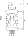
- Fig. 1 is a plan view illustrating a structure of a light-emitting device 10 of a first embodiment.
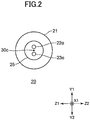
- Fig. 2 is an elevation view illustrating a structure of a light source unit 20 of the light-emitting device 10.
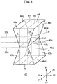
- Fig. 3 is a perspective view illustrating a structure of a prism 40 of the light-emitting device 10.
- an X-Y-Z coordinate is illustrated as a standard coordinate.
- An X1-X2 direction is a direction that extends along an optical axis 30c of a condenser lens 30, and a Y-Z plane is a plane that is perpendicular to the X1-X2 direction.
- the light-emitting device 10 includes the light source unit 20, the condenser lens 30 as a condensing optical system, and a prism 40 as a dioptric system.
- two laser diodes 22 and 23 as laser light sources are bonded to a stem 21. Further, a semiconductor chip (not illustrated in the drawings) for driving the laser diodes 22 and 23 and a lead frame (not illustrated in the drawings) for supporting the semiconductor chip are provided at the stem 21. A plurality of terminals 24 connected to the lead frame are extending outside by penetrating the stem 21 in the X2 direction. A hollow metal cap 25 is fixed to the stem 21 so as to cover the lead frame, the semiconductor chip and the laser diodes 22 and 23. Resin is filled in the cap 25, and with this, positions of the laser diodes 22 and 23 are fixed.
- the laser diodes 22 and 23 As illustrated in Fig. 1 and Fig. 2 , for the laser diodes 22 and 23, light exiting surfaces 22e and 23e are provided at a surface (a front end surface in the X1 direction) of the cap 25, respectively.
- the laser diodes 22 and 23 are provided such that their optical axes 22c and 23c, respectively, are in parallel to the optical axis 30c of the condenser lens 30.
- the condenser lens 30 as the condensing optical system is a double-convex plus lens.
- the condensing optical system it is not limited to the double-convex plus lens as illustrated in Fig. 1 , and as long as having a positive refractive power, a lens having another shape may be used. Further, not limited to a single lens, and an optical system in which a plurality of lenses are combined to have a condensing property may be used.
- the prism 40 includes two refraction parts 44 and 45 provided at an upper side and a lower side, respectively, in a Y1-Y2 direction. These refraction parts 44 and 45 have shapes that are symmetrical with respect to an XZ-plane. In the prism 40, the two refraction parts 44 and 45 are integrally formed using a glass or a plastic, for example.
- the first refraction part 44 of the prism 40 at a Y1 direction side has a bilateral symmetrical trapezoidal shape when seen in a Z1-Z2 direction.
- Two side surfaces 44c and 44d corresponding to an upper base and a lower base of the trapezoidal shape, are planes parallel to each other, and extending in the XZ-plane, respectively.
- An incident surface 44a and a light exiting surface 44b corresponding to remaining two sides of the trapezoidal shape, are planes each having an inclined angle such that a distance therebetween becomes larger as departing from the optical axis 30c of the condenser lens 30, and provided in this order from a light source unit 20 side in the X1-X2 direction.
- a vertex angle " ⁇ " is formed at a crossing position when seen in the Z1-Z2 direction ( Fig. 1 ).
- the incident surface 44a is inclined with respect to a plane S1 that is in parallel to the YZ-plane in an X2 direction side
- the light exiting surface 44b is inclined with respect to a plane S2 that is in parallel to the YZ-plane in an X1 direction side, wherein an inclined angle is " ⁇ ", respectively.
- the inclined angle " ⁇ " is set in accordance with an arrangement of the laser diode 22 with respect to the optical axis 30c of the condenser lens 30, a refractive index of the first refraction part 44, a refractive power of the condenser lens 30 or the like.
- the inclined angle " ⁇ " is set to be 1 / 2 of the vertex angle " ⁇ ".
- the second refraction part 45 of the prism 40 at a Y2 direction side has a bilateral symmetrical trapezoidal shape when seen in the Z1-Z2 direction.
- Two side surfaces 45c and 45d corresponding to an upper base and a lower base of the trapezoidal shape, are planes parallel to each other, and extending in the XZ-plane, respectively.
- An incident surface 45a and a light exiting surface 45b, corresponding to remaining two sides of the trapezoidal shape, are planes each having an inclined angle such that a distance therebetween becomes larger as departing from the optical axis 30c of the condenser lens 30, and provided in this order from the light source unit 20 side in the X1-X2 direction.
- a vertex angle " ⁇ " is formed at a crossing position when seen from the Z1-Z2 direction ( Fig. 1 ).
- the vertex angle formed by the incident surface 45a and the light exiting surface 45b is the same as the vertex angle formed by the incident surface 44a and the light exiting surface 44b.
- the incident surface 45a is inclined with respect to the plane S1 in the X2 direction side
- the light exiting surface 45b is inclined with respect to the plane S2 in the X1 direction, wherein an inclined angle is " ⁇ ", respectively.
- these inclined angles are set in accordance with an arrangement of the laser diode 23 with respect to the optical axis 30c of the condenser lens 30, a refractive index of the second refraction part 45, the refractive power of the condenser lens 30 or the like.
- this angle is the same as the inclined angle of the incident surface 44a and the light exiting surface 44b of the first refraction part 44.
- the side surface 44d of the first refraction part 44 and the side surface 45c of the second refraction part 45 are formed to be a common surface (shared surface), and as illustrated in Fig. 3 , the common surface is provided at the XZ-plane including the optical axis 30c of the condenser lens 30.
- the first refraction part 44 and the second refraction part 45 are provided to be symmetrical with respect to the XZ-plane.
- a center light beam 22a of an outgoing light ray from the laser diode 22 is input in the incident surface 44a in parallel to the optical axis 30c, and a center light beam 23a of an outgoing light ray from the laser diode 23 is input in the incident surface 45a in parallel to the optical axis 30c as well.
- the center light beam 22a is refracted in the first refraction part 44 in accordance with the refractive index of the first refraction part 44 and the setting of the inclined angle " ⁇ " of the incident surface 44a and the light exiting surface 44b to be output from the light exiting surface 44b.
- the refracted light ray 42a output from the light exiting surface 44b proceeds such that to depart from the optical axis 30c of the condenser lens 30 as proceeding toward a condenser lens 30 side.
- the center light beam 23a is refracted in the second refraction part 45 in accordance with the refractive index of the second refraction part 45, and the setting of the inclined angle " ⁇ " of the incident surface 45a and the light exiting surface 45b to be output from the light exiting surface 45b.
- the refracted light ray 43a output from the light exiting surface 45b proceeds such that to depart from the optical axis 30c of the condenser lens 30 as proceeding toward the condenser lens 30 side.
- the refracted light ray 42a and the refracted light ray 43a proceed to depart from each other as proceeding toward the condenser lens 30 side.
- the refracted light rays 42a and 43a output from the prism 40 are output from the condenser lens 30 as converging light rays 32a and 33a, respectively.
- Light fluxes of these converging light rays 32a and 33a overlap and become a pinpoint spot at a condensing position PC, and thereafter, images are formed at an image formation position PI, respectively.
- a light intensity per unit area can be increased at this position, and high-power can be obtained.
- the light intensity of the spot formed at the condensing position PC is approximately two times of each of the laser light rays output from the laser diodes 22 and 23, respectively.
- the condensing position PC is positioned at a back side of a back focal position PF of the condenser lens 30, in other words at a proceeded position of an image-side focal point in the X1 direction.
- the laser light rays output from the laser diodes 22 and 23 are directly input in the condenser lens 30 without using the prism 40, light fluxes are not overlapped at the back side of the back focal position PF to form a spot. Further, in such a case, portions of the two light fluxes may be overlapped at a front side of the back focal position PF, but the light fluxes do not form a spot at the position, and there exist portions where the light fluxes are overlapped and portions where the light fluxes are not overlapped. Thus, a light intensity per unit area is uneven, and the maximum value of the light intensity per unit area is approximately 1 to 1.5 times of a case when a single laser light is used.
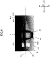
- Fig. 4 is a view illustrating a simulation model of a light-emitting device of example 1 of the first embodiment.
- Fig. 5 is a view illustrating a simulation model of a light-emitting device of a comparative example.
- Each of Fig. 4 and Fig. 5 illustrates a lens L corresponding to the condenser lens 30 of Fig. 1 , and an optical path in which light rays output from two laser diodes proceed from a left-side to a right-side.
- a prism D corresponding to the prism 40 of Fig. 1 is illustrated.
- FIG. 6 illustrate simulation results at positions P11, P12 and P13, respectively, in the model of example 1 illustrated in Fig. 4 .
- FIG. 7 illustrate simulation results at positions P21, P22 and P23, respectively, in the model of the comparative example illustrated in Fig. 5 .
- the position P11 of Fig. 4 and the position P21 of Fig. 5 correspond to the back focal position PF in Fig. 1
- the position P12 of Fig. 4 and the position P22 of Fig. 5 correspond to the condensing position PC in Fig. 1
- the position P13 of Fig. 4 and the position P23 of Fig. 5 correspond to the image formation position PI in Fig. 1 .
- example 1 illustrated in Fig. 4 light rays B11 and B12 are output from two laser diodes under the following conditions.
- the comparative example illustrated in Fig. 5 light rays B21 and B22 are output from two laser diodes, and a simulation was conducted under the same conditions as example 1 except that the prism D is not provided.
- an output of the laser diode was 1 W (watt) for both example 1 and the comparative example.
- Each of the following distances is a distance in a direction along an axis Lc of the lens L, and an axial distance means a distance on the optical axis Lc.
- both of the incident surface and the light exiting surface of each of the first refraction part 44 and the second refraction part 45 of the prism 40 are formed to be the inclined surfaces, respectively.
- the plurality of outgoing light rays from the first refraction part 44 and the second refraction part 45 can proceed such that a distance therebetween becomes larger as proceeding toward the condenser lens 30 side, only one of the incident surface and the light exiting surface may be formed to be the inclined surface.
- the inclined angles may be different for the incident surface and the light exiting surface.
- the inclined surface is not limited to a plane, and may be an aspheric surface or a hemispherical curved surface, or only an input area from each of the laser diodes 22 and 23 and an output area from the prism 40 may be configured by a desired inclined surface or a curved surface.
- the single prism 40 is used as the dioptric system.
- another configuration may be used.
- an optical member in which the outgoing light ray from the laser diode 22 is input, and an optical member in which the outgoing light ray from the laser diode 23 is input, may be separately provided.
- the two laser diodes 22 and 23 are provided such that their optical axes are in parallel to each other.
- the optical axes of the laser diodes 22 and 23 may be inclined by a predetermined angle with respect to the optical axis 30c of the condenser lens 30, respectively.
- the number of laser diodes, as the laser light sources are four.
- the same components as those described in the first embodiment are given the same reference numerals.
- Fig. 8 is an elevation view illustrating a structure of a light source unit 120 of a light-emitting device of a second embodiment.
- Fig. 9-(A) is a perspective view illustrating a structure of a prism 140 of the light-emitting device of the second embodiment
- Fig. 9-(B) is a plan view of the prism 140 illustrated in Fig. 9-(A) .
- center light beams 123a and 125a, and refracted light rays 143a and 145a are not illustrated.
- each laser diode 122, 123, 124 and 125 are provided as laser light sources such that each optical axis is positioned on a circle 120c whose center is the optical axis 30c of the condenser lens 30, and these laser diodes are bonded to the stem 21.
- Each optical axis of each of the laser diodes 122, 123, 124 and 125 is in parallel to the optical axis 30c of the condenser lens 30, similarly as the first embodiment.
- the laser diode 122 is provided at the Y1 direction side, the laser diode 123 is provided at the Z1 direction side, the laser diode 124 is provided at the Y2 direction side, and the laser diode 125 is provided at the Z2 side, with respect to the optical axis 30c.
- the prism 140 illustrated in Fig. 9-(A) and Fig. 9-(B) is used as the dioptric system.
- the prism 140 has a rectangular outer shape when seen in the X1-X2 direction, and four refraction parts 142, 143, 144 and 145 are provided to correspond to the four laser diodes 122, 123, 124 and 125, respectively.
- the refraction part 142 is provided at the Y1 direction side
- the refraction part 143 is provided at the Z1 direction side
- the refraction part 144 is provided at the Y2 direction
- the refraction part 145 is provided at the Z2, with respect to the optical axis 30c, with equiangular intervals.
- the four refraction parts 142, 143, 144 and 145 are integrally formed by using a glass or a plastic, for example.
- Each of the refraction parts 142, 143, 144 and 145 includes an incident surface to which an outgoing light ray from the respective laser diode 122, 123, 124 or 125 is input, and a light exiting surface from which the input light ray is output after being refracted, from the light source unit 120 side in this order in the X1-X2 direction.
- the incident surface and the light exiting surface of the same refraction part are planes including inclined angles such that a distance therebetween becomes larger as departing from the optical axis 30c of the condenser lens 30. For example, as illustrated in Fig.
- an incident surface 142b and a light exiting surface 142c are provided in the refraction part 142, and an incident surface 144b and a light exiting surface 144c are provided in the refraction part 144.
- the incident surface 142b is inclined toward the X2 direction side with respect to a plane S3 that is in parallel to the YZ-plane
- the light exiting surface 142c is inclined toward the X1 direction side with respect to a plane S4 that is in parallel to the YZ-plane
- each inclined angle is " ⁇ ".
- the incident surface 144b is inclined toward the X2 direction side with respect to the plane S3
- the light exiting surface 144c is inclined toward the X1 direction side with respect to the plane S4, and each inclined angle is " ⁇ ".
- the outgoing light rays (center light beams 122a, 123a, 124a and 125a) from the laser diodes 122, 123, 124 and 125 are input in the refraction parts 142, 143, 144 and 145, and refracted to be output to the condenser lens 30 as refracted light rays 142a, 143a, 144a and 145a, respectively.
- These refracted light rays proceed such that to depart from the optical axis 30c of the condenser lens 30 as proceeding toward the condenser lens 30 side and are input in the condenser lens 30, and light fluxes of the converging light rays condensed by the condenser lens 30 overlap at the condensing position PC to become a pinpoint spot.
- a planar shape of the prism 140 seen in the X1-X2 direction is configured to have a rectangular shape, as long as input areas from the laser diodes 122, 123, 124 and 125 and output areas of the refracted light rays, respectively, can be ensured, a shape other than the rectangular shape, for example, a circular shape may be used.
Landscapes
- Physics & Mathematics (AREA)
- General Physics & Mathematics (AREA)
- Optics & Photonics (AREA)
- Condensed Matter Physics & Semiconductors (AREA)
- Electromagnetism (AREA)
- Semiconductor Lasers (AREA)
Applications Claiming Priority (2)
| Application Number | Priority Date | Filing Date | Title |
|---|---|---|---|
| JP2015161163 | 2015-08-18 | ||
| PCT/JP2016/068148 WO2017029874A1 (ja) | 2015-08-18 | 2016-06-17 | 発光装置 |
Publications (2)
| Publication Number | Publication Date |
|---|---|
| EP3340404A1 true EP3340404A1 (de) | 2018-06-27 |
| EP3340404A4 EP3340404A4 (de) | 2018-07-18 |
Family
ID=58051126
Family Applications (1)
| Application Number | Title | Priority Date | Filing Date |
|---|---|---|---|
| EP16836866.0A Withdrawn EP3340404A4 (de) | 2015-08-18 | 2016-06-17 | Lichtemittierende vorrichtung |
Country Status (6)
| Country | Link |
|---|---|
| US (1) | US20180045969A1 (de) |
| EP (1) | EP3340404A4 (de) |
| JP (1) | JPWO2017029874A1 (de) |
| KR (1) | KR20180019724A (de) |
| CN (1) | CN107851961A (de) |
| WO (1) | WO2017029874A1 (de) |
Families Citing this family (6)
| Publication number | Priority date | Publication date | Assignee | Title |
|---|---|---|---|---|
| DE102017115964B4 (de) * | 2017-07-14 | 2020-04-02 | LIMO GmbH | Vorrichtung zur Erzeugung einer linienförmigen Intensitätsverteilung einer Laserstrahlung |
| KR102130645B1 (ko) * | 2017-12-28 | 2020-07-06 | (주)유남옵틱스 | 라인빔 형성장치 |
| US11231569B2 (en) * | 2018-06-13 | 2022-01-25 | Panasonic Corporation | Light-emitting device and illumination device |
| JP6536724B1 (ja) * | 2018-07-04 | 2019-07-03 | ウシオ電機株式会社 | 光源装置、プロジェクタ |
| CN114859640B (zh) * | 2022-05-09 | 2024-07-19 | 无锡视美乐激光显示科技有限公司 | 一种光整形系统、光源装置以及光源装置的设计方法 |
| WO2025162713A1 (en) * | 2024-02-01 | 2025-08-07 | Ams-Osram International Gmbh | Optoelectronic device |
Family Cites Families (8)
| Publication number | Priority date | Publication date | Assignee | Title |
|---|---|---|---|---|
| JP2001284730A (ja) * | 2000-03-31 | 2001-10-12 | Matsushita Electric Ind Co Ltd | 集光レーザ装置 |
| US6556352B2 (en) * | 2000-08-23 | 2003-04-29 | Apollo Instruments Inc. | Optical coupling system |
| DE102004058044B4 (de) * | 2004-12-01 | 2014-02-06 | Friedrich-Schiller-Universität Jena | Ortsfrequenzfiltervorrichtung und Verfahren zur Ortsfrequenzfilterung von Laserstrahlen |
| US7515346B2 (en) * | 2006-07-18 | 2009-04-07 | Coherent, Inc. | High power and high brightness diode-laser array for material processing applications |
| JP4353992B2 (ja) * | 2007-08-23 | 2009-10-28 | 三菱電機株式会社 | 照明用光源装置および画像表示装置 |
| JP5169136B2 (ja) * | 2007-10-22 | 2013-03-27 | 株式会社デンソー | レーザビーム照射装置 |
| US7639722B1 (en) * | 2007-10-29 | 2009-12-29 | The United States Of America As Represented By The Secretary Of The Air Force | Multifaceted prism to cause the overlap of beams from a stack of diode laser bars |
| DE102009010693A1 (de) * | 2009-02-26 | 2010-09-02 | Limo Patentverwaltung Gmbh & Co. Kg | Vorrichtung zur Homogenisierung von Laserstrahlung |
-
2016
- 2016-06-17 EP EP16836866.0A patent/EP3340404A4/de not_active Withdrawn
- 2016-06-17 KR KR1020187001999A patent/KR20180019724A/ko not_active Ceased
- 2016-06-17 WO PCT/JP2016/068148 patent/WO2017029874A1/ja not_active Ceased
- 2016-06-17 CN CN201680041997.2A patent/CN107851961A/zh active Pending
- 2016-06-17 JP JP2017535274A patent/JPWO2017029874A1/ja not_active Withdrawn
-
2017
- 2017-10-24 US US15/791,544 patent/US20180045969A1/en not_active Abandoned
Also Published As
| Publication number | Publication date |
|---|---|
| WO2017029874A1 (ja) | 2017-02-23 |
| EP3340404A4 (de) | 2018-07-18 |
| CN107851961A (zh) | 2018-03-27 |
| JPWO2017029874A1 (ja) | 2018-03-01 |
| KR20180019724A (ko) | 2018-02-26 |
| US20180045969A1 (en) | 2018-02-15 |
Similar Documents
| Publication | Publication Date | Title |
|---|---|---|
| EP3340404A1 (de) | Lichtemittierende vorrichtung | |
| US9753268B2 (en) | Reticle unit, optical instrument, and rifle scope | |
| US6443594B1 (en) | One-piece lens arrays for collimating and focusing light and led light generators using same | |
| US6069748A (en) | Laser line generator system | |
| KR101616635B1 (ko) | 레이저 합성 광학 장치 | |
| US10036842B2 (en) | Illumination device | |
| CA2957343C (en) | Device for shaping laser radiation | |
| US11789233B2 (en) | Objective, use of an objective, measurement system comprising an objective and use of a bi-aspherical plastic lens in an objective | |
| JP6222557B2 (ja) | 車両用灯具 | |
| EP2503377A1 (de) | Lichtquellenvorrichtung | |
| JP6482015B2 (ja) | レーザレーダ装置およびレーザレーダ装置の受光装置 | |
| JP6380531B2 (ja) | 光合成レーザ装置 | |
| CN110941097A (zh) | 激光周视探测的圆锥形视场发射光学系统 | |
| ES2886896T3 (es) | Dispositivo de iluminación homogénea que comprende una matriz de diodos láser | |
| JP6543825B2 (ja) | マイクロレンズアレイ | |
| US20220206283A1 (en) | Telescopic sight having two sighting points | |
| JP7414826B2 (ja) | フレネルレンズを有する照光式レチクルシステム | |
| CN110932076A (zh) | 大功率泵浦激光器 | |
| JP5430510B2 (ja) | レーザ加工装置 | |
| CN114296089B (zh) | 光学系统及激光雷达 | |
| JP2016119135A (ja) | 発光装置 | |
| KR20170013344A (ko) | 자동차 조명 응용예에 대한 광학 렌즈 패키지 | |
| US20110235360A1 (en) | Light source device for supplying light to fiber optic illumination system | |
| JP5097798B2 (ja) | 光ファイバ照明装置 | |
| RU2518588C2 (ru) | Лазерный дальномер |
Legal Events
| Date | Code | Title | Description |
|---|---|---|---|
| PUAI | Public reference made under article 153(3) epc to a published international application that has entered the european phase |
Free format text: ORIGINAL CODE: 0009012 |
|
| 17P | Request for examination filed |
Effective date: 20180201 |
|
| AK | Designated contracting states |
Kind code of ref document: A1 Designated state(s): AL AT BE BG CH CY CZ DE DK EE ES FI FR GB GR HR HU IE IS IT LI LT LU LV MC MK MT NL NO PL PT RO RS SE SI SK SM TR |
|
| AX | Request for extension of the european patent |
Extension state: BA ME |
|
| A4 | Supplementary search report drawn up and despatched |
Effective date: 20180618 |
|
| RIC1 | Information provided on ipc code assigned before grant |
Ipc: G02B 27/09 20060101ALN20180612BHEP Ipc: H01S 5/022 20060101AFI20180612BHEP Ipc: G02B 19/00 20060101ALN20180612BHEP |
|
| DAV | Request for validation of the european patent (deleted) | ||
| DAX | Request for extension of the european patent (deleted) | ||
| RAP1 | Party data changed (applicant data changed or rights of an application transferred) |
Owner name: ALPS ALPINE CO., LTD. |
|
| STAA | Information on the status of an ep patent application or granted ep patent |
Free format text: STATUS: THE APPLICATION HAS BEEN WITHDRAWN |
|
| 18W | Application withdrawn |
Effective date: 20190510 |