EP3340472A1 - Barrette de condensateurs de cna et convertisseur analogique-numérique, procédé de réduction de la consommation de puissance d'un convertisseur analogique-numérique - Google Patents
Barrette de condensateurs de cna et convertisseur analogique-numérique, procédé de réduction de la consommation de puissance d'un convertisseur analogique-numérique Download PDFInfo
- Publication number
- EP3340472A1 EP3340472A1 EP16898149.6A EP16898149A EP3340472A1 EP 3340472 A1 EP3340472 A1 EP 3340472A1 EP 16898149 A EP16898149 A EP 16898149A EP 3340472 A1 EP3340472 A1 EP 3340472A1
- Authority
- EP
- European Patent Office
- Prior art keywords
- capacitor
- bit
- sub
- significant
- capacitor array
- Prior art date
- Legal status (The legal status is an assumption and is not a legal conclusion. Google has not performed a legal analysis and makes no representation as to the accuracy of the status listed.)
- Ceased
Links
Images
Classifications
-
- H—ELECTRICITY
- H03—ELECTRONIC CIRCUITRY
- H03M—CODING; DECODING; CODE CONVERSION IN GENERAL
- H03M1/00—Analogue/digital conversion; Digital/analogue conversion
- H03M1/002—Provisions or arrangements for saving power, e.g. by allowing a sleep mode, using lower supply voltage for downstream stages, using multiple clock domains or by selectively turning on stages when needed
-
- H—ELECTRICITY
- H03—ELECTRONIC CIRCUITRY
- H03M—CODING; DECODING; CODE CONVERSION IN GENERAL
- H03M1/00—Analogue/digital conversion; Digital/analogue conversion
- H03M1/12—Analogue/digital converters
- H03M1/34—Analogue value compared with reference values
- H03M1/38—Analogue value compared with reference values sequentially only, e.g. successive approximation type
-
- H—ELECTRICITY
- H03—ELECTRONIC CIRCUITRY
- H03M—CODING; DECODING; CODE CONVERSION IN GENERAL
- H03M1/00—Analogue/digital conversion; Digital/analogue conversion
- H03M1/12—Analogue/digital converters
- H03M1/34—Analogue value compared with reference values
- H03M1/38—Analogue value compared with reference values sequentially only, e.g. successive approximation type
- H03M1/46—Analogue value compared with reference values sequentially only, e.g. successive approximation type with digital/analogue converter for supplying reference values to converter
- H03M1/466—Analogue value compared with reference values sequentially only, e.g. successive approximation type with digital/analogue converter for supplying reference values to converter using switched capacitors
- H03M1/468—Analogue value compared with reference values sequentially only, e.g. successive approximation type with digital/analogue converter for supplying reference values to converter using switched capacitors in which the input S/H circuit is merged with the feedback DAC array
-
- H—ELECTRICITY
- H03—ELECTRONIC CIRCUITRY
- H03M—CODING; DECODING; CODE CONVERSION IN GENERAL
- H03M1/00—Analogue/digital conversion; Digital/analogue conversion
- H03M1/12—Analogue/digital converters
- H03M1/34—Analogue value compared with reference values
- H03M1/38—Analogue value compared with reference values sequentially only, e.g. successive approximation type
- H03M1/46—Analogue value compared with reference values sequentially only, e.g. successive approximation type with digital/analogue converter for supplying reference values to converter
- H03M1/462—Details of the control circuitry, e.g. of the successive approximation register
Definitions
- Embodiments of the present disclosure relate to the technical field of integrated circuits, and in particular, relate to a DAC capacitor array, an analog-to-digital converter, and a method for reducing power consumption of an analog-to-digital converter.
- a successive approximation analog-to-digital converter is capable of converting an analog signal into a digital signal.
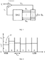
- the SAR ADC is formed of a comparator, a register and a digital-to-analog converter (DAC), the principle of converting the analog signal into the digital signal by the SAR ADC is: comparing an analog input signal to be converted with a reference signal which is acquired by an output of a D/A converter, determining to increase or decrease the digital signal input to the DAC according to the comparison result such that the reference signal approximates to the analog input signal, and when the reference signal is equal to the analog input signal, the digital signal input to the DAC is the digital signal corresponding to the analog input signal.
- the analog-to-digital conversion can be implemented by means of successive approximation of the DAC output to the input voltage, and the process of successive approximation may be referenced to FIG. 2 .
- the SAR ADC can be used as a key component for interfacing between an analog module and a digital module, and is extensively applied to mobile devices, wireless sensors and the like. Due to the size and endurance of the device, the analog-to-digital converter needs to have a small size and a low power consumption, such that the analog-to-digital converter can be conveniently integrated into the circuits of various devices.
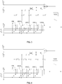
- Two types of DAC capacitor arrays applicable to the SAR analog-to-digital converter may be provided in the related art, as illustrated in FIG. 3 and FIG. 4 .
- FIG. 3 illustrates a conventional DAC capacitor array.
- Capacitors in the DAC capacitor array are not arranged in a binary weighting manner according to the capacitance values thereof.
- Each branch has the identical single-bit capacitors. Since the manufacturer error is proportional to the capacitance and area of the capacitor, the manufacture error may be reduced if the identical single-bit capacitors are employed. Relative to the capacitor arrays arranged in a binary weighting manner according to the capacitance values thereof, the size and power consumption of the entire capacitor array may be reduced when the identical single-bit capacitors are employed.
- this technical solution may have a problem that too many control branches are produced, which may directly cause an increase of size and power consumption of the control circuit. In this way, the advantages achieved by reduction of the capacitor area are reduced or even disappear.
- FIG. 4 illustrates another conventional DAC capacitor array.
- the other capacitors are arranged in a binary weighting manner according to the capacitance values thereof.
- the power consumption of the circuit may be effectively reduced by changing the reference voltage of the single-bit capacitors on the right side of the DAC capacitor array.
- the entire capacitor may be very large, the power consumption of the circuit may be increased, or even power consumption reduction achieved by changing the reference voltage of the right-side single-bit capacitor may be offset.
- embodiments of the present disclosure provide a DAC capacitor array, an analog-to-digital converter, and a method for reducing power consumption of a analog-to-digital converter, to reduce the entire capacitance of an SAR analog-to-digital converter, and thus may reduce the size of the analog-to-digital converter and reduce the power consumption.
- embodiments of the present disclosure provide a digital-to-analog converter (DAC) capacitor array, the DAC capacitor array being applied in an SAR analog-to-digital converter.
- the DAC capacitor array includes a plurality of sub-capacitor arrays that are connected in parallel, each of the plurality of sub-capacitor arrays including:
- the DAC capacitor array further includes a symmetric capacitor array; wherein one terminal of each capacitor in the symmetric capacitor array is connected to the other terminal of the comparator.
- the input source includes an analog input signal and a plurality of reference voltages
- the reference voltage has a voltage value range of 0 to V R
- reference voltages to which the significant-bit sub-capacitor group is connected include 0, V R 2 and V R
- reference voltages to which the non-significant-bit sub-capacitor group is connected include 2 M ⁇ 1 2 M + 1 V R , V R 2 and 2 M ⁇ 1 2 M + 1 V R
- V R has an adjustable value.
- inventions of the present disclosure provide a successive approximation (SAR) analog-to-digital converter.
- the SAR analog-to-digital converter includes a comparator, a register connected to an output terminal of the comparator, and a digital-to-analog converter (DAC) capacitor array connected to an input terminal of the comparator; wherein the DAC capacitor array includes:
- each of the plurality of sub-capacitor arrays including:
- the SAR analog-to-digital converter further includes a symmetric capacitor array; wherein one terminal of each capacitor in the symmetric capacitor array is connected to the other terminal of the comparator.
- the input source includes an analog input signal and a plurality of reference voltages
- the reference voltage has a voltage value range of 0 to V R
- reference voltages to which the significant-bit sub-capacitor group is connected include 0, V R 2 and V R
- reference voltages to which the non-significant-bit sub-capacitor group is connected include 2 M ⁇ 1 2 M + 1 V R , V R 2 and 2 M ⁇ 1 2 M + 1 V R
- V R has an adjustable value.
- the capacitors are arranged from high to low, capacitance values of the capacitors in the significant-bit sub-capacitor group are sequentially H P , H P-1 , ..., H 2 and H 1 , and capacitance values of the capacitors in the non-significant-bit sub-capacitor group are sequentially L M , L M-1 , ..., L 2 and L 1 ; wherein values of H P-1 V R , H 2 V R , ..., H 2 V R , H 1 V R , 1 2 M + 1 L M V R , 1 2 M + 1 L M ⁇ 1 V R , L M-1 V R , ..., 1 2 M + 1 L 2 V R , 1 2 M + 1 L 1 V R satisfy a geometric relation having a ratio of 2.
- embodiments of the present disclosure provide a method for reducing power consumption of a successive approximation (SAR) analog-to-digital converter.
- the method includes:
- selecting a corresponding sub-capacitor array according to the most-significant-bit value includes:
- the acquiring a second most-significant-bit value and a least-significant-bit value from the selected sub-capacitor array includes: adjusting the reference voltages of the capacitors in the selected sub-capacitor array as 2 M ⁇ 1 2 M + 1 V R or 2 M + 1 2 M + 1 V R according to the comparison result between the terminal voltage of the DAC capacitor array connected to one input terminal of the comparator and the voltage at the other input terminal of the comparator, wherein M is the number of capacitors in a non-significant-bit sub-capacitor group in the selected sub-capacitor array.
- the DAC capacitor array is optimized by adjusting the reference voltage to which the capacitors in the DAC capacitor array are connected, which reduces the overall capacitance of the DAC capacitor array. In this way, the size of the SAR analog-to-digital converter is reduced, the power consumption is reduced, and meanwhile the cost of chips may be lowered in manufacture of the chips. In addition, by modifying the conversion process between the analog signal and the digital signal, the voltage variation range between two terminals of the capacitor is narrowed and thus the overall power consumption is reduced.
- a DAC capacitor array is applied in an SAR analog-to-digital converter.
- a DAC capacitor array between a binary weighting-based DAC capacitor and a single-bit capacitor-based DAC capacitor array is disclosed by combining and changing the conventional two DAC capacitor arrays in the background.
- the DAC capacitor array includes a plurality of sub-capacitor arrays that are connected in parallel.
- the DAC capacitor array according to the embodiment of the present disclosure may be divided into a plurality of identical sub-capacitor arrays.
- each of the plurality of sub-capacitor arrays includes:
- the SAR analog-to-digital converter employing the above capacitor array is a single-ended SAR analog-to-digital converter, and has only one analog input which is sampled to the DAC capacitor array.
- the SAR analog-to-digital converter further includes a symmetric capacitor array; wherein one terminal of each capacitor in the symmetric capacitor array is connected to the other terminal of the comparator.
- the analog-to-digital converting including the symmetric capacitor array is a differential analog-to-digital converter, and correspondingly includes two inputs V ip and V in .
- V ip and V in are respectively sampled to two symmetric capacitor arrays, and are respectively connected to two input terminals of the comparator.
- the capacitor array to which V ip is input may be connected to a positive input terminal of the comparator, and the capacitor array to which V in is input may be connected to a negative input terminal of the comparator.
- the sub-capacitor array includes a plurality of capacitors, and the capacitor groups may be divided into a significant-bit sub-capacitor group, a non-significant-bit sub-capacitor group and a supplement-bit capacitor.
- the supplement-bit capacitor is a single-bit capacitor
- the significant-bit sub-capacitor group includes P capacitors
- the non-significant-bit sub-capacitor group includes M capacitors.
- Three capacitors may be single-bit capacitors, and the non-single-bit capacitors are arranged in a binary weighting manner according to the capacitance values.
- the capacitors in the sub-capacitor array may not be arranged in a binary weighting manner.
- the input source includes an analog input signal and a plurality of reference voltages
- the reference voltage has a voltage value range of 0 to V R
- reference voltages to which the significant-bit sub-capacitor group is connected include 0, V R 2 and V R
- reference voltages to which the non-significant-bit sub-capacitor group is connected includes 2 M ⁇ 1 2 M + 1 V R
- V R may have an adjustable value.
- capacitors are arranged from high to low, capacitance values of the capacitors in the significant-bit sub-capacitor group are sequentially H P , H P-1 , ..., H 2 and H 1 , and capacitance values of the capacitors in the non-significant-bit sub-capacitor group are sequentially L M , L M-1 , ..., L 2 and L 1 .
- values of H P-1 V R , H 2 V R , ..., H 2 V R , H 1 V R , 1 2 M + 1 L M V R , 1 2 M + 1 L M ⁇ 1 V R , ..., 1 2 M + 1 L 2 V R , 1 2 M + 1 L 1 V R satisfy a geometric relation having an equal ratio of 2.
- values of H P-1 V R , H 2 V R , ..., H 2 V R , H 1 V R , 1 2 M + 1 L M V R , 1 2 M + 1 L M ⁇ 1 V R , ..., 1 2 M + 1 L 2 V R , 1 2 M + 1 L 1 V R may satisfy a geometric relation having an equal ratio of any positive integer, or may not satisfy a geometric relation.
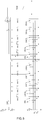
- the DAC capacitor array is divided into two identical sub-capacitor arrays, which includes a sub-capacitor array I and a sub-capacitor array II.
- the sub-capacitor array I and the sub-capacitor array II may be considered functionally similar to the single-bit capacitor as illustrated in FIG. 3 in the background.
- the value of the reference voltage connected to the non-significant-bit sub-capacitor group may affect division of the significant-bit sub-capacitor group and the non-significant-bit sub-capacitor group in the sub-capacitor array, and values of the capacitors in the sub-capacitor array, or the division of the significant-bit sub-capacitor group and the non-significant-bit sub-capacitor group in the sub-capacitor array may affect the values of the reference voltage connected to the non-significant-bit sub-capacitor group and the values of the capacitors in the sub-capacitor array.
- the significant-bit sub-capacitor group includes a capacitor C1 and a capacitor C2
- the non-significant-bit sub-capacitor group includes a capacitor C3.
- H P-1 V R , H 2 V R , ..., H 2 V R , H 1 V R , 1 2 M + 1 L M V R , 1 2 M + 1 L M ⁇ 1 V R , ..., 1 2 M + 1 L 2 V R , 1 2 M + 1 L 1 V R satisfy a geometric relation having an equal ratio of 2, in this case, C1 may be changed to have capacitance C, C2 may be changed to have capacitance 2C, and C3 and C4 remain unchanged. Nevertheless, the above values may also not satisfy the geometric relation having an equal ratio of 2, or may satisfy a geometric relation having a ratio of any other value.
- the capacitance values of the capacitors in the DAC capacitor array may be changed by adjusting the reference voltage, such that the single-bit capacitance of the DAC capacitor array may be reduced.
- the capacitance values of the capacitors may be arranged in a binary manner, or may be arranged in another manner instead of the binary manner.
- an SAR analog-to-digital converter includes the DAC capacitor array described in the above embodiment.
- a method for reducing power consumption of an SAR analog-to-digital converter is provided.
- C denotes the capacitance value of a capacitor
- V denotes a voltage variation on the capacitor.
- the capacitance value is determined by noise and matching.
- the noise refers to that resistance thermal noise enters to the capacitor via the sampling and is then superimposed on a useful signal
- the matching refers to that a manufactured capacitor is deviated from a design capacitor due to a limited precision in the manufacture, and thus a capacitance ratio of any two capacitors is inconsistent with the designed value, which affect the ADC precision to some extent.
- the voltage is determined by a dynamic range of the ADC, which specifically refers to an input voltage range of the ADC.
- the method for reducing power consumption of an SAR analog-to-digital converter includes the following steps:
- the significant-bit result of the SAR analog-to-digital converter determines in which sub-capacitor array the non-significant-bit conversion is carried out.
- the DAC capacitor array includes a sub-capacitor array I and a sub-capacitor array II. Specifically, if the most significant bit is 1, the non-significant-bit conversion is carried out in the sub-capacitor array I; and if the most significant bit is 0, the non-significant-bit conversion is carried out in the sub-capacitor array II.
- four sub-capacitor arrays may be employed. Specifically, one of the four sub-capacitor arrays is selected according to a result of the two most significant bits to determine the values of the remaining bits of a to-be-output digital signal.
- the selecting a corresponding sub-capacitor array according to the most-significant-bit value includes: connecting non-selected sub-capacitor arrays to a reference voltage 0 or a reference voltage V R when the sub-capacitor array is selected.
- the reference voltage to which the capacitors in each sub-capacitor array are connected is determined according to the significant-bit result of the SAR analog-to-digital converter.
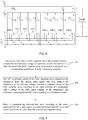
- the DAC capacitor array for use in a four-bit SAR analog-to-digital converter as illustrated in FIG. 6 , the DAC capacitor array includes a sub-capacitor array I and a sub-capacitor array II.
- the sub-capacitor array II may be connected to the reference voltage 0 and the non-significant-bit conversion is carried out in the sub-capacitor array I; and if the most significant bit is 0, the capacitors in the sub-capacitor array may be connected to the reference voltage V R and the non-significant-bit conversion is carried out in the sub-capacitor array II.
- the acquiring a second most-significant-bit value and a least-significant-bit value from the selected sub-capacitor array includes: adjusting the reference voltages of the capacitors in the selected sub-capacitor array as 2 M ⁇ 1 2 M + 1 V R or 2 M + 1 2 M + 1 V R according to the comparison result between the terminal voltage of the DAC capacitor array connected to one input terminal of the comparator and the voltage at the other input terminal of the comparator, wherein M is the number of capacitors in a non-significant-bit sub-capacitor group in the selected sub-capacitor array.
- the DAC capacitor array may be expanded to any plurality of sub-capacitor arrays.
- the significant bit value of the SAR analog-to-digital converter employing the expanded DAC capacitor array determines in which sub-capacitor array the non-significant-bit conversion is carried out.
- the method for reducing power consumption of an SAR analog-to-digital converter is described in detail with reference to a specific example.
- the four-bit SAR analog-to-digital converter employs the DAC capacitor array as illustrated in FIG. 6 .
- capacitor C1 and capacitor C5 are the most significant bits in the sub-capacitor array. Assume that the dynamic range of the SAR analog-to-digital converter is from V R to 0.
- the DAC capacitor array is divided into two identical sub-capacitor arrays, and these two identical sub-capacitor arrays may be considered functionally similar as the single-bit capacitor as illustrated in FIG. 3 in the background.
- the four-bit SAR analog-to-digital converter carries out analog-to-digital conversion as follows:
- the free terminal of the DAC capacitor array is connected to the analog signal V i via a multiplexer; meanwhile the common terminal of the capacitors are connected to the reference voltage V R 2 and are connected to the input terminal of the comparator; and the input voltage (the analog signal) V i is sampled to the free terminal of each capacitor in the DAC capacitor array as illustrated in FIG. 6 .
- Vx is greater than V R 2 , the free ends of the sub-capacitor array II may all be connected to the reference voltage 0, that is, connected to the ground.
- the reference voltage connected to the free ends of the capacitors in the sub-capacitor array I may only be changed.
- Vx is less than V R 2 , the free ends of the sub-capacitor array I may all be connected to the reference voltage V R .
- the reference voltage connected to the free ends of the capacitors in the sub-capacitor array II may only be changed.
- the capacitor arrangement in the high-precision SAR analog-to-digital converter may be optimized with respect to different process parameters, so as to reduce the power consumption and chip area.
- the number of capacitors in the capacitor array may be reduced by optimizing the DAC capacitor array, which reduces the overall capacitance of the DAC capacitor array. In this way, the size of the SAR analog-to-digital converter may be reduced, the power consumption may be reduced, and meanwhile the cost of chips may be lowered in manufacture of the chips.
- the voltage variation range between two terminals of the capacitor is narrowed and thus the overall power consumption may be reduced.
Landscapes
- Engineering & Computer Science (AREA)
- Theoretical Computer Science (AREA)
- Power Engineering (AREA)
- Analogue/Digital Conversion (AREA)
Applications Claiming Priority (1)
| Application Number | Priority Date | Filing Date | Title |
|---|---|---|---|
| PCT/CN2016/103185 WO2018076160A1 (fr) | 2016-10-25 | 2016-10-25 | Barrette de condensateurs de cna et convertisseur analogique-numérique, procédé de réduction de la consommation de puissance d'un convertisseur analogique-numérique |
Publications (2)
| Publication Number | Publication Date |
|---|---|
| EP3340472A1 true EP3340472A1 (fr) | 2018-06-27 |
| EP3340472A4 EP3340472A4 (fr) | 2018-07-04 |
Family
ID=58952262
Family Applications (1)
| Application Number | Title | Priority Date | Filing Date |
|---|---|---|---|
| EP16898149.6A Ceased EP3340472A4 (fr) | 2016-10-25 | 2016-10-25 | Barrette de condensateurs de cna et convertisseur analogique-numérique, procédé de réduction de la consommation de puissance d'un convertisseur analogique-numérique |
Country Status (5)
| Country | Link |
|---|---|
| US (1) | US10079609B2 (fr) |
| EP (1) | EP3340472A4 (fr) |
| KR (1) | KR101972689B1 (fr) |
| CN (1) | CN106797220B (fr) |
| WO (1) | WO2018076160A1 (fr) |
Families Citing this family (20)
| Publication number | Priority date | Publication date | Assignee | Title |
|---|---|---|---|---|
| CN108476024B (zh) * | 2016-09-23 | 2022-01-21 | 深圳市汇顶科技股份有限公司 | 一种dac电容阵列、sar型模数转换器及降低功耗的方法 |
| WO2018176326A1 (fr) * | 2017-03-30 | 2018-10-04 | 深圳市汇顶科技股份有限公司 | Circuit et procédé de conversion analogique-numérique |
| CN109643975B (zh) * | 2017-07-26 | 2023-06-16 | 深圳市汇顶科技股份有限公司 | 动态放大电路 |
| US11372032B2 (en) * | 2017-09-27 | 2022-06-28 | Texas Instruments Incorporated | Voltage monitor using a capacitive digital-to-analog converter |
| US10218376B1 (en) * | 2017-11-08 | 2019-02-26 | Xilinx, Inc. | Capacitive digital-to-analog converter |
| US10291252B1 (en) * | 2018-05-31 | 2019-05-14 | Shenzhen GOODIX Technology Co., Ltd. | Successive approximation register (SAR) analog to digital converter (ADC) dynamic range extension |
| CN108880553B (zh) * | 2018-07-05 | 2021-12-10 | 福建工程学院 | 低功耗自适应交替的逐次逼近型模数转换器及控制方法 |
| US10432213B1 (en) * | 2018-07-08 | 2019-10-01 | Shenzhen GOODIX Technology Co., Ltd. | Successive approximation register (SAR) analog to digital converter (ADC) with overlapping reference voltage ranges |
| CN109602438A (zh) * | 2018-12-12 | 2019-04-12 | 彭浩 | 高复用度的全身pet数据采集方法及系统 |
| CN109802680B (zh) * | 2018-12-18 | 2023-06-09 | 北京大学(天津滨海)新一代信息技术研究院 | 一种基于分数基准的电容阵列及模数转换器 |
| KR102661956B1 (ko) * | 2019-02-27 | 2024-04-29 | 삼성전자주식회사 | 아날로그 디지털 변환기 |
| US11206035B2 (en) * | 2019-03-13 | 2021-12-21 | Texas Instruments Incorporated | Analog to digital (A/D) converter with internal diagnostic circuit |
| US20210028159A1 (en) * | 2019-07-25 | 2021-01-28 | National Cheng Kung University | Symmetrical layout structure of semiconductor device |
| US10784883B1 (en) * | 2019-10-25 | 2020-09-22 | Qualcomm Incorporated | Noise shaping analog-to-digital converter |
| US11101811B2 (en) | 2019-12-06 | 2021-08-24 | Texas Instruments Incorporated | Systems and methods for testing analog to digital (A/D) converter with built-in diagnostic circuit with user supplied variable input voltage |
| CN112202447A (zh) * | 2020-09-28 | 2021-01-08 | 苏州锐迪联电子科技有限公司 | 一种新型数模转换结构 |
| KR20220050676A (ko) | 2020-10-16 | 2022-04-25 | 삼성전자주식회사 | 임피던스 측정 장치 |
| KR102871980B1 (ko) | 2021-06-16 | 2025-10-16 | 삼성전자주식회사 | 스플릿 인버터, 이를 포함하는 커패시터 디지털-아날로그 컨버터 및 연속 근사 레지스터 타입의 아날로그-디지털 컨버터 |
| CN114710160A (zh) * | 2022-04-08 | 2022-07-05 | 矽力杰半导体技术(杭州)有限公司 | 电容阵列失配的校准方法 |
| KR102816196B1 (ko) | 2023-04-14 | 2025-06-02 | 한양대학교 산학협력단 | 캐패시터들 사이의 미스매치로 인한 오차를 저감시키는 디지털-아날로그 컨버터 |
Family Cites Families (23)
| Publication number | Priority date | Publication date | Assignee | Title |
|---|---|---|---|---|
| US5606320A (en) * | 1994-12-06 | 1997-02-25 | Pacesetter Inc. | Method and apparatus for micropower analog-to-digital conversion in an implantable medical device |
| JPH1070463A (ja) * | 1996-08-26 | 1998-03-10 | Sony Corp | アナログ/ディジタル変換回路 |
| US6828927B1 (en) * | 2002-11-22 | 2004-12-07 | Analog Devices, Inc. | Successive approximation analog-to-digital converter with pre-loaded SAR registers |
| US6731232B1 (en) * | 2002-12-27 | 2004-05-04 | Analog Devices, Inc. | Programmable input range SAR ADC |
| US7286075B2 (en) * | 2005-11-14 | 2007-10-23 | Analog Devices, Inc. | Analog to digital converter with dither |
| JP2011188240A (ja) * | 2010-03-09 | 2011-09-22 | Panasonic Corp | 逐次比較型ad変換器、移動体無線装置 |
| EP2421155B1 (fr) * | 2010-08-02 | 2013-07-03 | Fraunhofer-Gesellschaft zur Förderung der Angewandten Forschung e.V. | Convertisseur hybride analogique-numérique, capteur d'images et procédé de fourniture d'une pluralité de signaux numériques |
| US8436677B2 (en) * | 2010-12-13 | 2013-05-07 | International Business Machines Corporation | Structure for a reference voltage generator for analog to digital converters |
| US8508400B2 (en) * | 2011-06-24 | 2013-08-13 | Mediatek Inc. | Successive approximation register analog to digital converter and conversion method thereof |
| US8981985B2 (en) * | 2011-09-06 | 2015-03-17 | National University Of Singapore | Analog-to-digital converter for a multi-channel signal acquisition system |
| US8638248B2 (en) * | 2011-10-07 | 2014-01-28 | Nxp, B.V. | Input-independent self-calibration method and apparatus for successive approximation analog-to-digital converter with charge-redistribution digital to analog converter |
| CN103441765B (zh) * | 2011-10-27 | 2016-08-10 | 财团法人成大研究发展基金会 | 逐渐逼近模拟至数字转换器及其方法 |
| KR101299215B1 (ko) * | 2012-03-12 | 2013-08-22 | 전자부품연구원 | 커패시터 부정합 교정 방법 및 이를 이용하는 아날로그 디지털 변환 장치 |
| CN102801422B (zh) * | 2012-08-17 | 2016-06-15 | 中国科学院微电子研究所 | 逐次逼近型模数转换器 |
| CN104734716B (zh) * | 2013-12-24 | 2017-12-12 | 瑞昱半导体股份有限公司 | 连续逼近暂存式模拟数字转换器及其控制方法 |
| US9300316B2 (en) * | 2014-02-28 | 2016-03-29 | Qualcomm Incorporated | Voltage doubling circuit for an analog to digital converter (ADC) |
| CN103905049B (zh) * | 2014-03-11 | 2017-11-03 | 中国科学院半导体研究所 | 一种高速快闪加交替比较式逐次逼近模数转换器 |
| CN104113340B (zh) * | 2014-07-07 | 2017-01-18 | 西安电子科技大学 | 一种无寄存器异步逐次逼近型模数转换器 |
| KR101501881B1 (ko) * | 2014-07-31 | 2015-03-19 | 중앙대학교 산학협력단 | 분리 형태의 듀얼 캐패시터 어레이를 가지는 연속 근사 레지스터 아날로그 디지털 변환기 |
| WO2016061784A1 (fr) * | 2014-10-23 | 2016-04-28 | Lattice Semiconductor Corporation | Convertisseur analogique-numérique basé sur un registre à approximations successives avec plage temporelle augmentée pour la stabilisation des condensateurs numérique-analogique |
| US10135453B2 (en) * | 2016-01-06 | 2018-11-20 | Disruptive Technologies Research As | SAR ADC with threshold trigger functionality for reduced power consumption |
| US9654131B1 (en) * | 2016-02-26 | 2017-05-16 | Texas Instruments Deutschland Gmbh | Capacitor order determination in an analog-to-digital converter |
| US10340932B2 (en) * | 2016-04-29 | 2019-07-02 | Analog Devices, Inc. | Techniques for power efficient oversampling successive approximation register |
-
2016
- 2016-10-25 CN CN201680001422.8A patent/CN106797220B/zh active Active
- 2016-10-25 KR KR1020177029837A patent/KR101972689B1/ko active Active
- 2016-10-25 EP EP16898149.6A patent/EP3340472A4/fr not_active Ceased
- 2016-10-25 WO PCT/CN2016/103185 patent/WO2018076160A1/fr not_active Ceased
-
2017
- 2017-10-16 US US15/784,514 patent/US10079609B2/en active Active
Also Published As
| Publication number | Publication date |
|---|---|
| KR101972689B1 (ko) | 2019-04-25 |
| US20180115317A1 (en) | 2018-04-26 |
| CN106797220B (zh) | 2020-10-20 |
| US10079609B2 (en) | 2018-09-18 |
| EP3340472A4 (fr) | 2018-07-04 |
| WO2018076160A1 (fr) | 2018-05-03 |
| KR20180062975A (ko) | 2018-06-11 |
| CN106797220A (zh) | 2017-05-31 |
Similar Documents
| Publication | Publication Date | Title |
|---|---|---|
| EP3340472A1 (fr) | Barrette de condensateurs de cna et convertisseur analogique-numérique, procédé de réduction de la consommation de puissance d'un convertisseur analogique-numérique | |
| US20180091163A1 (en) | Dac capacitor array, sar analog-to-digital converter and method for reducing power consumption thereof | |
| US7675452B2 (en) | Successive approximation register analog to digital converter with improved immunity to time varying noise | |
| US8842027B2 (en) | Analog to digital converter and method for evaluating capacitor weighting of digital-to-analog converter thereof | |
| US10097198B1 (en) | Sar adc | |
| CN105959006B (zh) | 逐次逼近型模数转换器校准电路 | |
| US8653998B2 (en) | D/A conversion circuit, A/D conversion circuit and electronic apparatus | |
| KR101299215B1 (ko) | 커패시터 부정합 교정 방법 및 이를 이용하는 아날로그 디지털 변환 장치 | |
| US20100060500A1 (en) | Analog/Digital Converter Assembly and Corresponding Method | |
| CN104124967A (zh) | 一种分段电容阵列型逐次逼近模数转换器校准结构及方法 | |
| CN108055037A (zh) | 一种逐次逼近型模数转换器及其开关切换方法 | |
| US10374625B2 (en) | Capacitor layout of digital-to-analog conversion integrated circuit | |
| US11050432B2 (en) | Pseudo differential analog-to-digital converter | |
| CN102055475B (zh) | 逐次逼近模拟数字转换器及其方法 | |
| US10985773B2 (en) | Analog to digital converting device and capacitor adjusting method thereof | |
| CN106972860B (zh) | 一种逐次逼近型模数转换器及其开关方法 | |
| KR20050050767A (ko) | 온-칩 기준전압 발생장치를 구비하는 반도체 칩 | |
| US20200127676A1 (en) | Calibration method and related calibration system | |
| CN107835023B (zh) | 一种逐次逼近型数模转换器 | |
| CN214799459U (zh) | 逐次逼近型模数转换装置 | |
| US7034724B2 (en) | Training circuit and method of digital-analog converter and analog-digital converter | |
| Fan et al. | Capacitive recombination calibration method to improve the performance of SAR ADC | |
| CN115051710B (zh) | 逐次逼近型模数转换装置 | |
| CN114024550A (zh) | 模数转换器和自动化配电设备 | |
| CN108964662B (zh) | 集成电路电容布局 |
Legal Events
| Date | Code | Title | Description |
|---|---|---|---|
| STAA | Information on the status of an ep patent application or granted ep patent |
Free format text: STATUS: UNKNOWN |
|
| STAA | Information on the status of an ep patent application or granted ep patent |
Free format text: STATUS: THE INTERNATIONAL PUBLICATION HAS BEEN MADE |
|
| PUAI | Public reference made under article 153(3) epc to a published international application that has entered the european phase |
Free format text: ORIGINAL CODE: 0009012 |
|
| STAA | Information on the status of an ep patent application or granted ep patent |
Free format text: STATUS: REQUEST FOR EXAMINATION WAS MADE |
|
| 17P | Request for examination filed |
Effective date: 20171018 |
|
| AK | Designated contracting states |
Kind code of ref document: A1 Designated state(s): AL AT BE BG CH CY CZ DE DK EE ES FI FR GB GR HR HU IE IS IT LI LT LU LV MC MK MT NL NO PL PT RO RS SE SI SK SM TR |
|
| AX | Request for extension of the european patent |
Extension state: BA ME |
|
| A4 | Supplementary search report drawn up and despatched |
Effective date: 20180606 |
|
| RIC1 | Information provided on ipc code assigned before grant |
Ipc: H03M 1/46 20060101ALI20180530BHEP Ipc: H03M 1/00 20060101AFI20180530BHEP |
|
| DAV | Request for validation of the european patent (deleted) | ||
| DAX | Request for extension of the european patent (deleted) | ||
| STAA | Information on the status of an ep patent application or granted ep patent |
Free format text: STATUS: EXAMINATION IS IN PROGRESS |
|
| 17Q | First examination report despatched |
Effective date: 20190529 |
|
| REG | Reference to a national code |
Ref country code: DE Ref legal event code: R003 |
|
| STAA | Information on the status of an ep patent application or granted ep patent |
Free format text: STATUS: THE APPLICATION HAS BEEN REFUSED |
|
| 18R | Application refused |
Effective date: 20211031 |