EP3340752A1 - Luftdurchlässiges temporäres trägerband zur einbettung einer komponente in einem komponententräger - Google Patents
Luftdurchlässiges temporäres trägerband zur einbettung einer komponente in einem komponententräger Download PDFInfo
- Publication number
- EP3340752A1 EP3340752A1 EP16206288.9A EP16206288A EP3340752A1 EP 3340752 A1 EP3340752 A1 EP 3340752A1 EP 16206288 A EP16206288 A EP 16206288A EP 3340752 A1 EP3340752 A1 EP 3340752A1
- Authority
- EP
- European Patent Office
- Prior art keywords
- component
- tape
- base structure
- accommodation
- hole
- Prior art date
- Legal status (The legal status is an assumption and is not a legal conclusion. Google has not performed a legal analysis and makes no representation as to the accuracy of the status listed.)
- Granted
Links
Images



Classifications
-
- H—ELECTRICITY
- H05—ELECTRIC TECHNIQUES NOT OTHERWISE PROVIDED FOR
- H05K—PRINTED CIRCUITS; CASINGS OR CONSTRUCTIONAL DETAILS OF ELECTRIC APPARATUS; MANUFACTURE OF ASSEMBLAGES OF ELECTRICAL COMPONENTS
- H05K1/00—Printed circuits
- H05K1/02—Details
- H05K1/0272—Adaptations for fluid transport, e.g. channels, holes
-
- H—ELECTRICITY
- H05—ELECTRIC TECHNIQUES NOT OTHERWISE PROVIDED FOR
- H05K—PRINTED CIRCUITS; CASINGS OR CONSTRUCTIONAL DETAILS OF ELECTRIC APPARATUS; MANUFACTURE OF ASSEMBLAGES OF ELECTRICAL COMPONENTS
- H05K1/00—Printed circuits
- H05K1/18—Printed circuits structurally associated with non-printed electric components
- H05K1/182—Printed circuits structurally associated with non-printed electric components associated with components mounted in printed circuit boards [PCB], e.g. insert-mounted components [IMC]
- H05K1/185—Printed circuits structurally associated with non-printed electric components associated with components mounted in printed circuit boards [PCB], e.g. insert-mounted components [IMC] associated with components encapsulated in the insulating substrate of the PCBs; associated with components incorporated in internal layers of multilayer circuit boards
-
- B—PERFORMING OPERATIONS; TRANSPORTING
- B32—LAYERED PRODUCTS
- B32B—LAYERED PRODUCTS, i.e. PRODUCTS BUILT-UP OF STRATA OF FLAT OR NON-FLAT, e.g. CELLULAR OR HONEYCOMB, FORM
- B32B15/00—Layered products comprising a layer of metal
- B32B15/04—Layered products comprising a layer of metal comprising metal as the main or only constituent of a layer, which is next to another layer of the same or of a different material
- B32B15/08—Layered products comprising a layer of metal comprising metal as the main or only constituent of a layer, which is next to another layer of the same or of a different material of synthetic resin
-
- B—PERFORMING OPERATIONS; TRANSPORTING
- B32—LAYERED PRODUCTS
- B32B—LAYERED PRODUCTS, i.e. PRODUCTS BUILT-UP OF STRATA OF FLAT OR NON-FLAT, e.g. CELLULAR OR HONEYCOMB, FORM
- B32B15/00—Layered products comprising a layer of metal
- B32B15/14—Layered products comprising a layer of metal next to a fibrous or filamentary layer
-
- B—PERFORMING OPERATIONS; TRANSPORTING
- B32—LAYERED PRODUCTS
- B32B—LAYERED PRODUCTS, i.e. PRODUCTS BUILT-UP OF STRATA OF FLAT OR NON-FLAT, e.g. CELLULAR OR HONEYCOMB, FORM
- B32B15/00—Layered products comprising a layer of metal
- B32B15/20—Layered products comprising a layer of metal comprising aluminium or copper
-
- B—PERFORMING OPERATIONS; TRANSPORTING
- B32—LAYERED PRODUCTS
- B32B—LAYERED PRODUCTS, i.e. PRODUCTS BUILT-UP OF STRATA OF FLAT OR NON-FLAT, e.g. CELLULAR OR HONEYCOMB, FORM
- B32B27/00—Layered products comprising a layer of synthetic resin
- B32B27/06—Layered products comprising a layer of synthetic resin as the main or only constituent of a layer, which is next to another layer of the same or of a different material
-
- B—PERFORMING OPERATIONS; TRANSPORTING
- B32—LAYERED PRODUCTS
- B32B—LAYERED PRODUCTS, i.e. PRODUCTS BUILT-UP OF STRATA OF FLAT OR NON-FLAT, e.g. CELLULAR OR HONEYCOMB, FORM
- B32B27/00—Layered products comprising a layer of synthetic resin
- B32B27/06—Layered products comprising a layer of synthetic resin as the main or only constituent of a layer, which is next to another layer of the same or of a different material
- B32B27/08—Layered products comprising a layer of synthetic resin as the main or only constituent of a layer, which is next to another layer of the same or of a different material of synthetic resin
-
- B—PERFORMING OPERATIONS; TRANSPORTING
- B32—LAYERED PRODUCTS
- B32B—LAYERED PRODUCTS, i.e. PRODUCTS BUILT-UP OF STRATA OF FLAT OR NON-FLAT, e.g. CELLULAR OR HONEYCOMB, FORM
- B32B27/00—Layered products comprising a layer of synthetic resin
- B32B27/12—Layered products comprising a layer of synthetic resin next to a fibrous or filamentary layer
-
- B—PERFORMING OPERATIONS; TRANSPORTING
- B32—LAYERED PRODUCTS
- B32B—LAYERED PRODUCTS, i.e. PRODUCTS BUILT-UP OF STRATA OF FLAT OR NON-FLAT, e.g. CELLULAR OR HONEYCOMB, FORM
- B32B27/00—Layered products comprising a layer of synthetic resin
- B32B27/28—Layered products comprising a layer of synthetic resin comprising synthetic resins not wholly covered by any one of the sub-groups B32B27/30 - B32B27/42
- B32B27/281—Layered products comprising a layer of synthetic resin comprising synthetic resins not wholly covered by any one of the sub-groups B32B27/30 - B32B27/42 comprising polyimides
-
- B—PERFORMING OPERATIONS; TRANSPORTING
- B32—LAYERED PRODUCTS
- B32B—LAYERED PRODUCTS, i.e. PRODUCTS BUILT-UP OF STRATA OF FLAT OR NON-FLAT, e.g. CELLULAR OR HONEYCOMB, FORM
- B32B27/00—Layered products comprising a layer of synthetic resin
- B32B27/32—Layered products comprising a layer of synthetic resin comprising polyolefins
- B32B27/322—Layered products comprising a layer of synthetic resin comprising polyolefins comprising halogenated polyolefins, e.g. PTFE
-
- B—PERFORMING OPERATIONS; TRANSPORTING
- B32—LAYERED PRODUCTS
- B32B—LAYERED PRODUCTS, i.e. PRODUCTS BUILT-UP OF STRATA OF FLAT OR NON-FLAT, e.g. CELLULAR OR HONEYCOMB, FORM
- B32B27/00—Layered products comprising a layer of synthetic resin
- B32B27/34—Layered products comprising a layer of synthetic resin comprising polyamides
-
- B—PERFORMING OPERATIONS; TRANSPORTING
- B32—LAYERED PRODUCTS
- B32B—LAYERED PRODUCTS, i.e. PRODUCTS BUILT-UP OF STRATA OF FLAT OR NON-FLAT, e.g. CELLULAR OR HONEYCOMB, FORM
- B32B27/00—Layered products comprising a layer of synthetic resin
- B32B27/38—Layered products comprising a layer of synthetic resin comprising epoxy resins
-
- B—PERFORMING OPERATIONS; TRANSPORTING
- B32—LAYERED PRODUCTS
- B32B—LAYERED PRODUCTS, i.e. PRODUCTS BUILT-UP OF STRATA OF FLAT OR NON-FLAT, e.g. CELLULAR OR HONEYCOMB, FORM
- B32B3/00—Layered products comprising a layer with external or internal discontinuities or unevennesses, or a layer of non-planar shape; Layered products comprising a layer having particular features of form
- B32B3/02—Layered products comprising a layer with external or internal discontinuities or unevennesses, or a layer of non-planar shape; Layered products comprising a layer having particular features of form characterised by features of form at particular places, e.g. in edge regions
- B32B3/08—Layered products comprising a layer with external or internal discontinuities or unevennesses, or a layer of non-planar shape; Layered products comprising a layer having particular features of form characterised by features of form at particular places, e.g. in edge regions characterised by added members at particular parts
-
- B—PERFORMING OPERATIONS; TRANSPORTING
- B32—LAYERED PRODUCTS
- B32B—LAYERED PRODUCTS, i.e. PRODUCTS BUILT-UP OF STRATA OF FLAT OR NON-FLAT, e.g. CELLULAR OR HONEYCOMB, FORM
- B32B3/00—Layered products comprising a layer with external or internal discontinuities or unevennesses, or a layer of non-planar shape; Layered products comprising a layer having particular features of form
- B32B3/26—Layered products comprising a layer with external or internal discontinuities or unevennesses, or a layer of non-planar shape; Layered products comprising a layer having particular features of form characterised by a particular shape of the outline of the cross-section of a continuous layer; characterised by a layer with cavities or internal voids ; characterised by an apertured layer
- B32B3/30—Layered products comprising a layer with external or internal discontinuities or unevennesses, or a layer of non-planar shape; Layered products comprising a layer having particular features of form characterised by a particular shape of the outline of the cross-section of a continuous layer; characterised by a layer with cavities or internal voids ; characterised by an apertured layer characterised by a layer formed with recesses or projections, e.g. hollows, grooves, protuberances, ribs
-
- B—PERFORMING OPERATIONS; TRANSPORTING
- B32—LAYERED PRODUCTS
- B32B—LAYERED PRODUCTS, i.e. PRODUCTS BUILT-UP OF STRATA OF FLAT OR NON-FLAT, e.g. CELLULAR OR HONEYCOMB, FORM
- B32B5/00—Layered products characterised by the non- homogeneity or physical structure, i.e. comprising a fibrous, filamentary, particulate or foam layer; Layered products characterised by having a layer differing constitutionally or physically in different parts
- B32B5/22—Layered products characterised by the non- homogeneity or physical structure, i.e. comprising a fibrous, filamentary, particulate or foam layer; Layered products characterised by having a layer differing constitutionally or physically in different parts characterised by the presence of two or more layers which are next to each other and are fibrous, filamentary, formed of particles or foamed
- B32B5/24—Layered products characterised by the non- homogeneity or physical structure, i.e. comprising a fibrous, filamentary, particulate or foam layer; Layered products characterised by having a layer differing constitutionally or physically in different parts characterised by the presence of two or more layers which are next to each other and are fibrous, filamentary, formed of particles or foamed one layer being a fibrous or filamentary layer
-
- B—PERFORMING OPERATIONS; TRANSPORTING
- B32—LAYERED PRODUCTS
- B32B—LAYERED PRODUCTS, i.e. PRODUCTS BUILT-UP OF STRATA OF FLAT OR NON-FLAT, e.g. CELLULAR OR HONEYCOMB, FORM
- B32B7/00—Layered products characterised by the relation between layers; Layered products characterised by the relative orientation of features between layers, or by the relative values of a measurable parameter between layers, i.e. products comprising layers having different physical, chemical or physicochemical properties; Layered products characterised by the interconnection of layers
- B32B7/04—Interconnection of layers
- B32B7/06—Interconnection of layers permitting easy separation
-
- B—PERFORMING OPERATIONS; TRANSPORTING
- B32—LAYERED PRODUCTS
- B32B—LAYERED PRODUCTS, i.e. PRODUCTS BUILT-UP OF STRATA OF FLAT OR NON-FLAT, e.g. CELLULAR OR HONEYCOMB, FORM
- B32B7/00—Layered products characterised by the relation between layers; Layered products characterised by the relative orientation of features between layers, or by the relative values of a measurable parameter between layers, i.e. products comprising layers having different physical, chemical or physicochemical properties; Layered products characterised by the interconnection of layers
- B32B7/04—Interconnection of layers
- B32B7/12—Interconnection of layers using interposed adhesives or interposed materials with bonding properties
-
- B—PERFORMING OPERATIONS; TRANSPORTING
- B32—LAYERED PRODUCTS
- B32B—LAYERED PRODUCTS, i.e. PRODUCTS BUILT-UP OF STRATA OF FLAT OR NON-FLAT, e.g. CELLULAR OR HONEYCOMB, FORM
- B32B9/00—Layered products comprising a layer of a particular substance not covered by groups B32B11/00 - B32B29/00
- B32B9/04—Layered products comprising a layer of a particular substance not covered by groups B32B11/00 - B32B29/00 comprising such particular substance as the main or only constituent of a layer, which is next to another layer of the same or of a different material
- B32B9/045—Layered products comprising a layer of a particular substance not covered by groups B32B11/00 - B32B29/00 comprising such particular substance as the main or only constituent of a layer, which is next to another layer of the same or of a different material of synthetic resin
-
- B—PERFORMING OPERATIONS; TRANSPORTING
- B32—LAYERED PRODUCTS
- B32B—LAYERED PRODUCTS, i.e. PRODUCTS BUILT-UP OF STRATA OF FLAT OR NON-FLAT, e.g. CELLULAR OR HONEYCOMB, FORM
- B32B9/00—Layered products comprising a layer of a particular substance not covered by groups B32B11/00 - B32B29/00
- B32B9/04—Layered products comprising a layer of a particular substance not covered by groups B32B11/00 - B32B29/00 comprising such particular substance as the main or only constituent of a layer, which is next to another layer of the same or of a different material
- B32B9/047—Layered products comprising a layer of a particular substance not covered by groups B32B11/00 - B32B29/00 comprising such particular substance as the main or only constituent of a layer, which is next to another layer of the same or of a different material made of fibres or filaments
-
- C—CHEMISTRY; METALLURGY
- C09—DYES; PAINTS; POLISHES; NATURAL RESINS; ADHESIVES; COMPOSITIONS NOT OTHERWISE PROVIDED FOR; APPLICATIONS OF MATERIALS NOT OTHERWISE PROVIDED FOR
- C09J—ADHESIVES; NON-MECHANICAL ASPECTS OF ADHESIVE PROCESSES IN GENERAL; ADHESIVE PROCESSES NOT PROVIDED FOR ELSEWHERE; USE OF MATERIALS AS ADHESIVES
- C09J7/00—Adhesives in the form of films or foils
- C09J7/20—Adhesives in the form of films or foils characterised by their carriers
- C09J7/22—Plastics; Metallised plastics
-
- H—ELECTRICITY
- H05—ELECTRIC TECHNIQUES NOT OTHERWISE PROVIDED FOR
- H05K—PRINTED CIRCUITS; CASINGS OR CONSTRUCTIONAL DETAILS OF ELECTRIC APPARATUS; MANUFACTURE OF ASSEMBLAGES OF ELECTRICAL COMPONENTS
- H05K3/00—Apparatus or processes for manufacturing printed circuits
- H05K3/30—Assembling printed circuits with electric components, e.g. with resistors
- H05K3/303—Assembling printed circuits with electric components, e.g. with resistors with surface mounted components
- H05K3/305—Affixing by adhesive
-
- B—PERFORMING OPERATIONS; TRANSPORTING
- B32—LAYERED PRODUCTS
- B32B—LAYERED PRODUCTS, i.e. PRODUCTS BUILT-UP OF STRATA OF FLAT OR NON-FLAT, e.g. CELLULAR OR HONEYCOMB, FORM
- B32B2255/00—Coating on the layer surface
- B32B2255/20—Inorganic coating
- B32B2255/205—Metallic coating
-
- B—PERFORMING OPERATIONS; TRANSPORTING
- B32—LAYERED PRODUCTS
- B32B—LAYERED PRODUCTS, i.e. PRODUCTS BUILT-UP OF STRATA OF FLAT OR NON-FLAT, e.g. CELLULAR OR HONEYCOMB, FORM
- B32B2260/00—Layered product comprising an impregnated, embedded, or bonded layer wherein the layer comprises an impregnation, embedding, or binder material
- B32B2260/02—Composition of the impregnated, bonded or embedded layer
- B32B2260/021—Fibrous or filamentary layer
-
- B—PERFORMING OPERATIONS; TRANSPORTING
- B32—LAYERED PRODUCTS
- B32B—LAYERED PRODUCTS, i.e. PRODUCTS BUILT-UP OF STRATA OF FLAT OR NON-FLAT, e.g. CELLULAR OR HONEYCOMB, FORM
- B32B2260/00—Layered product comprising an impregnated, embedded, or bonded layer wherein the layer comprises an impregnation, embedding, or binder material
- B32B2260/04—Impregnation, embedding, or binder material
- B32B2260/046—Synthetic resin
-
- B—PERFORMING OPERATIONS; TRANSPORTING
- B32—LAYERED PRODUCTS
- B32B—LAYERED PRODUCTS, i.e. PRODUCTS BUILT-UP OF STRATA OF FLAT OR NON-FLAT, e.g. CELLULAR OR HONEYCOMB, FORM
- B32B2262/00—Composition or structural features of fibres which form a fibrous or filamentary layer or are present as additives
- B32B2262/10—Inorganic fibres
- B32B2262/101—Glass fibres
-
- B—PERFORMING OPERATIONS; TRANSPORTING
- B32—LAYERED PRODUCTS
- B32B—LAYERED PRODUCTS, i.e. PRODUCTS BUILT-UP OF STRATA OF FLAT OR NON-FLAT, e.g. CELLULAR OR HONEYCOMB, FORM
- B32B2307/00—Properties of the layers or laminate
- B32B2307/20—Properties of the layers or laminate having particular electrical or magnetic properties, e.g. piezoelectric
- B32B2307/202—Conductive
-
- B—PERFORMING OPERATIONS; TRANSPORTING
- B32—LAYERED PRODUCTS
- B32B—LAYERED PRODUCTS, i.e. PRODUCTS BUILT-UP OF STRATA OF FLAT OR NON-FLAT, e.g. CELLULAR OR HONEYCOMB, FORM
- B32B2307/00—Properties of the layers or laminate
- B32B2307/20—Properties of the layers or laminate having particular electrical or magnetic properties, e.g. piezoelectric
- B32B2307/206—Insulating
-
- B—PERFORMING OPERATIONS; TRANSPORTING
- B32—LAYERED PRODUCTS
- B32B—LAYERED PRODUCTS, i.e. PRODUCTS BUILT-UP OF STRATA OF FLAT OR NON-FLAT, e.g. CELLULAR OR HONEYCOMB, FORM
- B32B2307/00—Properties of the layers or laminate
- B32B2307/30—Properties of the layers or laminate having particular thermal properties
- B32B2307/302—Conductive
-
- B—PERFORMING OPERATIONS; TRANSPORTING
- B32—LAYERED PRODUCTS
- B32B—LAYERED PRODUCTS, i.e. PRODUCTS BUILT-UP OF STRATA OF FLAT OR NON-FLAT, e.g. CELLULAR OR HONEYCOMB, FORM
- B32B2307/00—Properties of the layers or laminate
- B32B2307/70—Other properties
- B32B2307/724—Permeability to gases, adsorption
-
- B—PERFORMING OPERATIONS; TRANSPORTING
- B32—LAYERED PRODUCTS
- B32B—LAYERED PRODUCTS, i.e. PRODUCTS BUILT-UP OF STRATA OF FLAT OR NON-FLAT, e.g. CELLULAR OR HONEYCOMB, FORM
- B32B2307/00—Properties of the layers or laminate
- B32B2307/70—Other properties
- B32B2307/724—Permeability to gases, adsorption
- B32B2307/7242—Non-permeable
- B32B2307/7244—Oxygen barrier
-
- B—PERFORMING OPERATIONS; TRANSPORTING
- B32—LAYERED PRODUCTS
- B32B—LAYERED PRODUCTS, i.e. PRODUCTS BUILT-UP OF STRATA OF FLAT OR NON-FLAT, e.g. CELLULAR OR HONEYCOMB, FORM
- B32B2307/00—Properties of the layers or laminate
- B32B2307/70—Other properties
- B32B2307/748—Releasability
-
- B—PERFORMING OPERATIONS; TRANSPORTING
- B32—LAYERED PRODUCTS
- B32B—LAYERED PRODUCTS, i.e. PRODUCTS BUILT-UP OF STRATA OF FLAT OR NON-FLAT, e.g. CELLULAR OR HONEYCOMB, FORM
- B32B2457/00—Electrical equipment
- B32B2457/08—PCBs, i.e. printed circuit boards
-
- C—CHEMISTRY; METALLURGY
- C09—DYES; PAINTS; POLISHES; NATURAL RESINS; ADHESIVES; COMPOSITIONS NOT OTHERWISE PROVIDED FOR; APPLICATIONS OF MATERIALS NOT OTHERWISE PROVIDED FOR
- C09J—ADHESIVES; NON-MECHANICAL ASPECTS OF ADHESIVE PROCESSES IN GENERAL; ADHESIVE PROCESSES NOT PROVIDED FOR ELSEWHERE; USE OF MATERIALS AS ADHESIVES
- C09J2203/00—Applications of adhesives in processes or use of adhesives in the form of films or foils
- C09J2203/326—Applications of adhesives in processes or use of adhesives in the form of films or foils for bonding electronic components such as wafers, chips or semiconductors
-
- C—CHEMISTRY; METALLURGY
- C09—DYES; PAINTS; POLISHES; NATURAL RESINS; ADHESIVES; COMPOSITIONS NOT OTHERWISE PROVIDED FOR; APPLICATIONS OF MATERIALS NOT OTHERWISE PROVIDED FOR
- C09J—ADHESIVES; NON-MECHANICAL ASPECTS OF ADHESIVE PROCESSES IN GENERAL; ADHESIVE PROCESSES NOT PROVIDED FOR ELSEWHERE; USE OF MATERIALS AS ADHESIVES
- C09J2301/00—Additional features of adhesives in the form of films or foils
- C09J2301/10—Additional features of adhesives in the form of films or foils characterized by the structural features of the adhesive tape or sheet
- C09J2301/18—Additional features of adhesives in the form of films or foils characterized by the structural features of the adhesive tape or sheet characterized by perforations in the adhesive tape
-
- C—CHEMISTRY; METALLURGY
- C09—DYES; PAINTS; POLISHES; NATURAL RESINS; ADHESIVES; COMPOSITIONS NOT OTHERWISE PROVIDED FOR; APPLICATIONS OF MATERIALS NOT OTHERWISE PROVIDED FOR
- C09J—ADHESIVES; NON-MECHANICAL ASPECTS OF ADHESIVE PROCESSES IN GENERAL; ADHESIVE PROCESSES NOT PROVIDED FOR ELSEWHERE; USE OF MATERIALS AS ADHESIVES
- C09J2463/00—Presence of epoxy resin
-
- H—ELECTRICITY
- H05—ELECTRIC TECHNIQUES NOT OTHERWISE PROVIDED FOR
- H05K—PRINTED CIRCUITS; CASINGS OR CONSTRUCTIONAL DETAILS OF ELECTRIC APPARATUS; MANUFACTURE OF ASSEMBLAGES OF ELECTRICAL COMPONENTS
- H05K2203/00—Indexing scheme relating to apparatus or processes for manufacturing printed circuits covered by H05K3/00
- H05K2203/01—Tools for processing; Objects used during processing
- H05K2203/0147—Carriers and holders
- H05K2203/0156—Temporary polymeric carrier or foil, e.g. for processing or transferring
-
- H—ELECTRICITY
- H05—ELECTRIC TECHNIQUES NOT OTHERWISE PROVIDED FOR
- H05K—PRINTED CIRCUITS; CASINGS OR CONSTRUCTIONAL DETAILS OF ELECTRIC APPARATUS; MANUFACTURE OF ASSEMBLAGES OF ELECTRICAL COMPONENTS
- H05K2203/00—Indexing scheme relating to apparatus or processes for manufacturing printed circuits covered by H05K3/00
- H05K2203/01—Tools for processing; Objects used during processing
- H05K2203/0147—Carriers and holders
- H05K2203/016—Temporary inorganic, non-metallic carrier, e.g. for processing or transferring
-
- H—ELECTRICITY
- H05—ELECTRIC TECHNIQUES NOT OTHERWISE PROVIDED FOR
- H05K—PRINTED CIRCUITS; CASINGS OR CONSTRUCTIONAL DETAILS OF ELECTRIC APPARATUS; MANUFACTURE OF ASSEMBLAGES OF ELECTRICAL COMPONENTS
- H05K2203/00—Indexing scheme relating to apparatus or processes for manufacturing printed circuits covered by H05K3/00
- H05K2203/11—Treatments characterised by their effect, e.g. heating, cooling, roughening
- H05K2203/1178—Means for venting or for letting gases escape
-
- H—ELECTRICITY
- H05—ELECTRIC TECHNIQUES NOT OTHERWISE PROVIDED FOR
- H05K—PRINTED CIRCUITS; CASINGS OR CONSTRUCTIONAL DETAILS OF ELECTRIC APPARATUS; MANUFACTURE OF ASSEMBLAGES OF ELECTRICAL COMPONENTS
- H05K2203/00—Indexing scheme relating to apparatus or processes for manufacturing printed circuits covered by H05K3/00
- H05K2203/13—Moulding and encapsulation; Deposition techniques; Protective layers
- H05K2203/1305—Moulding and encapsulation
-
- H—ELECTRICITY
- H05—ELECTRIC TECHNIQUES NOT OTHERWISE PROVIDED FOR
- H05K—PRINTED CIRCUITS; CASINGS OR CONSTRUCTIONAL DETAILS OF ELECTRIC APPARATUS; MANUFACTURE OF ASSEMBLAGES OF ELECTRICAL COMPONENTS
- H05K3/00—Apparatus or processes for manufacturing printed circuits
- H05K3/46—Manufacturing multilayer circuits
- H05K3/4602—Manufacturing multilayer circuits characterized by a special circuit board as base or central core whereon additional circuit layers are built or additional circuit boards are laminated
-
- H—ELECTRICITY
- H10—SEMICONDUCTOR DEVICES; ELECTRIC SOLID-STATE DEVICES NOT OTHERWISE PROVIDED FOR
- H10W—GENERIC PACKAGES, INTERCONNECTIONS, CONNECTORS OR OTHER CONSTRUCTIONAL DETAILS OF DEVICES COVERED BY CLASS H10
- H10W70/00—Package substrates; Interposers; Redistribution layers [RDL]
- H10W70/60—Insulating or insulated package substrates; Interposers; Redistribution layers
-
- H—ELECTRICITY
- H10—SEMICONDUCTOR DEVICES; ELECTRIC SOLID-STATE DEVICES NOT OTHERWISE PROVIDED FOR
- H10W—GENERIC PACKAGES, INTERCONNECTIONS, CONNECTORS OR OTHER CONSTRUCTIONAL DETAILS OF DEVICES COVERED BY CLASS H10
- H10W72/00—Interconnections or connectors in packages
- H10W72/90—Bond pads, in general
- H10W72/941—Dispositions of bond pads
- H10W72/9413—Dispositions of bond pads on encapsulations
Definitions
- the invention relates to a tape, a semifinished product, a method of manufacturing a component carrier, and a method of use.
- a tape for temporarily supporting one or more components during embedding in a base structure comprising a carrier foil, an adhesive applied on at least a part of at least one main surface of the carrier foil, and at least one airflow opening extending through the tape for enabling air to flow through the tape.
- a semifinished product which comprises a base structure (such as a core) having at least one accommodation through hole for accommodating a component (in particular an electronic component), and a tape having the above mentioned features adhered to at least a portion of a main surface of the base structure and only partially bridging (i.e. keeping partially open) the at least one accommodation through hole of the base structure.
- a base structure such as a core
- a tape having the above mentioned features adhered to at least a portion of a main surface of the base structure and only partially bridging (i.e. keeping partially open) the at least one accommodation through hole of the base structure.
- a method of manufacturing a component carrier comprises adhering a tape on at least part of a main surface of a base structure having at least one accommodation through hole for accommodating a component, placing at least one component in the at least one accommodation through hole on or above the tape, at least partially filling the at least one accommodation through hole with a filler material, and removing air bubbles in the filler material through the tape.
- an adhesive temporary tape with one or more airflow channels is used for embedding a component in a component carrier, in particular a printed circuit board.
- component carrier may particularly denote any support structure which is capable of accommodating one or more components thereon and/or therein for providing mechanical support and/or electrical connectivity.
- a component carrier may be configured as a mechanical and/or electronic carrier for components.
- a component carrier may be one of a printed circuit board, an organic interposer, and an IC (integrated circuit) substrate.
- a component carrier may also be a hybrid board combining different ones of the above mentioned types of component carriers.
- the term “electronic component” may particularly denote any bulky rather than layer-type active (such as a semiconductor chip) or passive (for instance a copper block) component embedded within an interior of the component carrier.
- a semifinished product may particularly denote a physical structure which is not yet readily manufactured but requires further processing to obtain a final product which can functionally serve as stand-alone component carrier.
- a semifinished product may be a pre-form of a component carrier to be manufactured based on the semifinished product.
- a sticky tape with one or more airflow openings is provided which is configured to be attached to a base structure during embedding of a component. Thanks to the provision of the one or more airflow openings, air bubbles and the like which may be present in adhesive material used for filling a gap between the component and the base structure/the sticky tape may escape from the arrangement via or through the airflow opening(s) of the air permeable tape. Therefore, a partially open rather than fully close temporary adhesive tape, capable of breathing during the embedding procedure, may be advantageously used for the embedding procedure so that the amount of undesired air bubbles within the accommodation through hole may be reduced. Therefore, the reproducibility and reliability (in terms of electrical, mechanical, thermal performance) of the manufactured component carrier can be significantly improved.
- the base structure comprises at least one of the group consisting of a core (in particular a fully cured core, for instance an already completely cross-linked core of resin and reinforcing fibers such as FR4) and a resin structure (in particular an at least partially uncured resin structure, for example a cut-out layer of prepreg, which may comprise resin with reinforcing particles embedded therein).
- a core in particular a fully cured core, for instance an already completely cross-linked core of resin and reinforcing fibers such as FR4
- a resin structure in particular an at least partially uncured resin structure, for example a cut-out layer of prepreg, which may comprise resin with reinforcing particles embedded therein.
- the base structure may also be a metal foil or metal layer, for instance cut-out or patterned.
- the term "core” may particularly denote already cured electrically insulating material providing a stable base for embedding one or more components.
- a core may be made of cured resin (such as epoxy resin) with fibers (such as glass fibers) embedded therein, for example FR4.
- a core may be made of a thickness being higher than that of a single layer (such as a prepreg layer) as used in PCB technology.
- the term "fully cured” may particularly denote a material property according to which the corresponding material (such as resin) is not capable any more of being remelted to become flowable and of being subsequently re-solidified for interconnecting various elements of the manufactured component carrier.
- resin material of the fully cured core may be already cross-linked.
- the fully cured core material may be C-stage material rather than A-stage or B-stage material.
- the carrier foil is an air-permeable membrane.
- an air permeable membrane can provide a high mounting surface for the component and at the same time an efficient airflow capability.
- the at least one airflow opening comprises at least one macroscopic through-hole.
- the at least one airflow opening comprises a pattern of through-holes (which may in particular extend in parallel through the carrier foil).
- a pattern or array may for instance be a regular pattern (for instance a matrix-like pattern of airflow openings in rows and columns) or an arbitrary pattern.
- a diameter of the at least one airflow opening is at least 10 ⁇ m, in particular is in a range between 10 ⁇ m and 500 ⁇ m. This ensures an efficient gas removal from the accommodation through hole.
- the dimension of the airflow openings may be below 25 ⁇ m, since this maintains a high stability of the tape while allowing for a sufficiently strong air communication through the thickness of the preferably bendable tape.
- At least one of the at least one airflow opening is located in a surface of the tape being uncovered (i.e. being not covered) with the component.
- At least one of the at least one airflow opening is located in a surface of the tape being covered (after mounting) with the component.
- the semifinished product further comprises at least one component accommodated in the at least one accommodation through hole.
- a component may be selected from a group consisting of an electrically non-conductive inlay, an electrically conductive inlay (such as a metal inlay, preferably comprising copper or aluminum), a heat transfer unit (for example a heat pipe), a light guiding element (for example an optical waveguide or a light conductor connection), an electronic component, or combinations thereof.
- the component can be an active electronic component, a passive electronic component, an electronic chip, a storage device (for instance a DRAM or another data memory), a filter, an integrated circuit, a signal processing component, a power management component, an optoelectronic interface element, a voltage converter (for example a DC/DC converter or an AC/DC converter), a cryptographic component, a transmitter and/or receiver, an electromechanical transducer, a sensor, an actuator, a microelectromechanical system (MEMS), a microprocessor, a capacitor, a resistor, an inductance, a battery, a switch, a camera, an antenna, a logic chip, and an energy harvesting unit.
- other components may be embedded in the component carrier.
- a magnetic element can be used as a component.
- a magnetic element may be a permanent magnetic element (such as a ferromagnetic element, an antiferromagnetic element or a ferrimagnetic element, for instance a ferrite core) or may be a paramagnetic element.
- the component may also be a further component carrier, for example in a board-in-board configuration.
- the component may be surface mounted on the component carrier and/or may be embedded in an interior thereof.
- other components in particular those which generate and emit electromagnetic radiation and/or are sensitive with regard to electromagnetic radiation propagating from an environment, may be used as component.
- the semifinished product comprises liquid adhesive as filler material filling at least part of a gap between the base structure and/or the tape on the one hand and at least one component in the at least one accommodation through hole on the other hand.
- liquid adhesive material may be filled into the accommodation through hole before and/or after mounting the component in the accommodation through hole (the latter being only partially bridged by the for instance flexible tape).
- the semifinished product comprises at least one electrically insulating layer structure laminated on the base structure and at least one component in the at least one accommodation through hole, wherein part of the at least one electrically insulating layer structure serves as filler material filling at least part of a gap between the base structure and the at least one component.
- layer structure may particularly denote one or more full or continuous layers, one or more patterned layers, and/or a plurality of islands-type separate elements formed together within a plane. Therefore, the air bubble removing function of the tape may also be applied to an architecture in which flowable resin, liquefied by lamination, of a laminated layer structure flows into a gap between base structure and electronic component.
- the at least one airflow opening is formed by at least one of the group consisting of a laser treatment (in particular UV laser treatment or Excimer laser treatment), and mechanically drilling.
- a laser treatment in particular UV laser treatment or Excimer laser treatment
- mechanically drilling for instance, etching
- other airflow opening manufacturing procedures for instance etching
- the at least one airflow opening is formed in the tape after adhering the tape to the base structure.
- the tape may have its full support capability while mounting the component, and can be recessed selectively afterwards at one or more desired locations for permitting gas flow through the membrane.
- the at least one airflow opening is formed in the tape before adhering the tape to the base structure.
- the tape may be provided with preformed airflow openings which accelerates the embedding procedure, since no formation of airflow openings is necessary during the embedding procedure.
- air bubbles in the filler material are removed at least partially through the tape by at least one of a vacuum treatment and an elevated temperature treatment.
- a vacuum treatment and the formation of an elevated temperature is advantageous for triggering efficient removal of gas bubbles.
- mobility of the air bubbles may be increased and the air bubbles may be triggered to leave (in particular may be sucked out) of the adhesive, wherein the airflow opening(s) of the tape ensure(s) an efficient removal of at least part of the air bubbles out of the adhesive.
- the filler material is provided by inserting a liquid adhesive into a gap between the base structure and/or the tape on the one hand and at least one component in the at least one accommodation through hole on the other hand.
- a liquid adhesive may be for instance an epoxy resin adhesive.
- the filler material is provided by laminating a resin comprising layer structure on the base structure and the component so that resin being liquefied during lamination flows into gaps between the base structure and the component in the accommodation through-hole.
- a dielectric layer structure may for instance be a resin layer or a prepreg layer, or, more generally, an at least partially uncured dielectric layer.
- the term "at least partially uncured material” particularly denotes material which has the property to at least partially melt or become flowable by the application of elevated pressure and/or elevated temperature, and become fully hardened or cured (and thereby becomes solid) when releasing the applied elevated pressure and/or elevated temperature.
- the "at least partially uncured material” may comprise or consist of B-stage material and/or A-stage material.
- the tape is removed from the base structure and the component after supplying the filler material.
- the temporary tape may be removed, for instance by peeling it off.
- the tape may remain part of the final product, i.e. of the component carrier manufactured as described herein.
- the component carrier or the preform thereof comprises a stack of at least one electrically insulating layer structure and at least one electrically conductive layer structure.
- the component carrier may be a laminate of the mentioned electrically insulating layer structure(s) and electrically conductive layer structure(s), in particular formed by applying mechanical pressure, if desired supported by thermal energy.
- the mentioned stack may provide a plate-shaped component carrier capable of providing a large mounting surface for further components and being nevertheless very thin and compact.
- layer structure may particularly denote a continuous layer, a patterned layer or a plurality of non-consecutive islands within a common plane.
- the component carrier or the preform thereof is shaped as a plate. This contributes to the compact design, wherein the component carrier nevertheless provides a large basis for mounting components thereon. Furthermore, in particular a naked die as example for an embedded electronic component, can be conveniently embedded, thanks to its small thickness, into a thin plate such as a printed circuit board.
- the component carrier is configured as one of the group consisting of a printed circuit board, and a substrate (in particular an IC substrate).
- PCB printed circuit board
- a component carrier which may be plate-shaped (i.e. planar), three-dimensionally curved (for instance when manufactured using 3D printing) or which may have any other shape) which is formed by laminating several electrically conductive layer structures with several electrically insulating layer structures, for instance by applying pressure, if desired accompanied by the supply of thermal energy.
- the electrically conductive layer structures are made of copper
- the electrically insulating layer structures may comprise resin and/or glass fibers, so-called prepreg or FR4 material.
- the various electrically conductive layer structures may be connected to one another in a desired way by forming through-holes through the laminate, for instance by laser drilling or mechanical drilling, and by filling them with electrically conductive material (in particular copper), thereby forming vias as through-hole connections.
- electrically conductive material in particular copper
- a printed circuit board is usually configured for accommodating one or more components on one or both opposing surfaces of the plate-shaped printed circuit board. They may be connected to the respective main surface by soldering.
- a dielectric part of a PCB may be composed of resin with reinforcing fibers (such as glass fibers).
- the term "substrate” may particularly denote a small component carrier having substantially the same size as a component (in particular an electronic component) to be mounted thereon. More specifically, a substrate can be understood as a carrier for electrical connections or electrical networks as well as component carrier comparable to a printed circuit board (PCB), however with a considerably higher density of laterally and/or vertically arranged connections. Lateral connections are for example conductive paths, whereas vertical connections may be for example drill holes. These lateral and/or vertical connections are arranged within the substrate and can be used to provide electrical and/or mechanical connections of housed components or unhoused components (such as bare dies), particularly of IC chips, with a printed circuit board or intermediate printed circuit board. Thus, the term “substrate” also includes "IC substrates". A dielectric part of a substrate may be composed of resin with reinforcing spheres (such as glass spheres).
- the at least one electrically insulating layer structure comprises at least one of the group consisting of resin (such as reinforced or non-reinforced resins, for instance epoxy resin or Bismaleimide-Triazine resin, more specifically FR-4 or FR-5), cyanate ester, polyphenylene derivate, glass (in particular glass fibers, multi-layer glass, glass-like materials), prepreg material, polyimide, polyamide, liquid crystal polymer (LCP), epoxy-based Build-Up Film, polytetrafluoroethylene (Teflon), a ceramic, and a metal oxide. Reinforcing materials such as webs, fibers or spheres, for example made of glass (multilayer glass) may be used as well.
- resin such as reinforced or non-reinforced resins, for instance epoxy resin or Bismaleimide-Triazine resin, more specifically FR-4 or FR-5
- cyanate ester polyphenylene derivate
- glass in particular glass fibers, multi-layer glass, glass-like materials
- prepreg or FR4 are usually preferred, other materials may be used as well.
- high-frequency materials such as polytetrafluoroethylene, liquid crystal polymer and/or cyanate ester resins may be implemented in the component carrier as electrically insulating layer structure.
- At least one electrically conductive layer structure of the preform comprises at least one of the group consisting of copper, aluminum, nickel, silver, gold, palladium, and tungsten.
- copper is usually preferred, other materials or coated versions thereof are possible as well, in particular coated with supra-conductive material such as graphene.
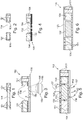
- Figure 1 to Figure 6 illustrate different cross-sectional views of structures obtained during carrying out a method of manufacturing a component carrier according to an exemplary embodiment of the invention.
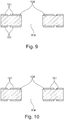
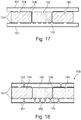
- Figure 7 to Figure 19 illustrate different cross-sectional views of structures obtained during carrying out a method of manufacturing a component carrier according to another exemplary embodiment of the invention.
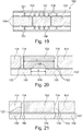
- Figure 20 and Figure 21 illustrate different cross-sectional views of tapes carrying structures obtained during carrying out a method of manufacturing a component carrier according to yet other exemplary embodiments of the invention.
- a highly reliable embedded component package may be provided in which issues resulting from air bubbles in temporarily flowable dielectric material are prevented.
- an exemplary embodiment of the invention provides a bubble-poor or even bubble-free embedding process for active and passive components, sensors, interposers, or even board-in-board devices. This makes it possible to reliably avoid an undesired floating of embedded parts under a vacuum process and guarantees an accurate registration process.
- exemplary embodiments of the invention make it possible to embed components of different sizes and shapes.
- High thermally conductive, mechanically robust and electrical reliable properties of a manufactured component carrier may be achieved. This advantageously results in a reliable behaviour of the manufactured component carrier in harsh environment, avoiding air inclusions. This drastically reduces the probability of oxidation of the component and the path for the electrochemical migration.
- a design of an embedded package with very high filling degree and consequent a significantly improved reliability in terms of thermal, chemical, mechanical and/or electrical properties may be achieved.
- a corresponding manufacturing method for a component carrier comprises cavity cutting in a structured base structure, and sticky tape lamination on one side.
- the adhesive tape may advantageously include clearances or openings, for instance in size below 25 ⁇ m.
- the airflow openings or clearances can be positioned under the embedded parts, in the cavity area or both.
- a resin or adhesive may be applied.
- the adhesive can have a viscosity in the range between 0,5 Pa ⁇ s to 300 Pa ⁇ s, in particular between 1 Pa ⁇ s to 150 Pa ⁇ s.
- the resin should be solvent free and also have a good floating behaviour with low surface tension.
- a vacuum process may be applied for a certain duration depending on the base structure thickness.
- the pressure can be less than 200 mbar during the vacuum treatment. It is then possible to apply a curing cycle according to the selected adhesive or resin. Subsequently, the tape may be removed. A layup and pressing process may be carried out. Furthermore, it is possible to connect the embedded part to the next layer.
- the included clearances in the tape allow running the vacuum process without any floating of the embedded part.
- the air under the embedded part may flow through the clearance when starting the vacuum.
- the embedded part may get a reliable adhesion to the tape and may offer a proper registration for further processes.
- the adhesion properties may be higher and the contacting pads may be free of plugged adhesive.
- bubbles trapped in the resin or adhesive, especially in the cavity corners may flow through the clearance of the cavity offside of the structure. Thereby, a homogeneous thermo-mechanical behaviour may be obtained, and the delamination risk may be suppressed. Beyond this, contamination and moisture tests have proven the especially high reliability of such packages or component carriers.
- the above mentioned selected range of the viscosity of the filler material allows a reliable bubble removal and avoids the resin or adhesive flowing through the tape.
- the fact that the resin (or adhesive) is solvent free avoids boiling effects caused by the vacuum process.
- the described process makes it possible to embed substantially all component sizes and shapes.
- Packages of component carriers manufactured following the described processes show high mechanical, thermal and electrical reliability. In other words, such a manufacturing method office highly reliable embedded packages of component carriers. Moreover, a high yield can be obtained.
- the described manufacturing procedure is also compatible with a large choice of materials and thereby provides a board designer with a high degree of flexibility.
- Figure 1 to Figure 6 illustrate different cross-sectional views of structures obtained during carrying out a method of manufacturing a component carrier 118 according to an exemplary embodiment of the invention.
- a base structure 104 which can be a core may be made of a fully cured material such as FR4.
- An electrically conductive layer structure 151 is formed partially on and partially in the base structure 104 and comprises patterned electrically conductive layers (for instance copper foils) on both opposing main surfaces of the base structure 104 as well as a vertical through connection (embodied as a copper filled via).
- the vertical through connection may be formed by mechanically drilling and copper plating.
- a sticky tape 100 is laminated to a lower main surface of the structure shown in Figure 2 .
- the tape 100 is configured for temporarily supporting electronic components 102 (compare Figure 4 ) during embedding in the base structure 104.
- the tape 100 comprises a carrier foil 106 (for instance made of a plastic material), an adhesive 108 (such as an epoxy resin) applied on the upper main surface of the carrier foil 106, and airflow openings 110 extending vertically through the entire tape 100 for enabling gas such as air to flow through the tape 100.
- the airflow openings 110 may be formed by a laser treatment (in particular UV laser treatment or Excimer laser treatment), or by mechanically drilling.
- the airflow openings 110 are already readily formed in the tape 100 before adhering the tape 100 to the base structure 104.
- the airflow openings 110 (which may also be denoted as air channels) are arranged as a pattern of through-holes extending in parallel through the carrier foil 106 and the layer of adhesive 108.
- a diameter, d, of the airflow openings 110 may be for example 20 ⁇ m. This maintains tightness for a viscous liquid material (see reference numeral 120 below) but allows gas to stream or flow from the accommodation through hole 114 through the tape 100 into an environment.
- semifinished product 112 is obtained which is composed of the base structure 104 with the accommodation through hole 114 for accommodating electronic component 102, and the tape 100 adhered to the lower main surface of the base structure 104 and only partially bridging the accommodation through hole 114 of the base structure 104.
- "Only partially bridging” hereby means that intentionally not the whole accommodation through hole 114 is closed by the tape 100, in contrast to this a flow of gaseous medium through the airflow openings 110 remains intentionally enabled.
- the airflow openings 110 are located in and extend from a surface of the tape 100 being later covered with the electronic component 102.
- the shown semifinished product 112 forms a preform of such a component carrier 118 to be manufactured (compare Figure 6 ), here configured as a printed circuit board (PCB).
- PCB printed circuit board
- an electronic component 102 may be assembled with the structure shown in Figure 3 . More specifically, the electronic component 102 (which may for instance be a semiconductor chip, here with pads face down) may be accommodated in the accommodation through hole 114 being partially bridged by the sticky tape 100 with its airflow openings 110 being located on a mounting surface of the electronic component 102. Thus, the electronic component 102 is placed in the accommodation through hole 114 and on the tape 100 so that the airflow openings 110 are located beneath the electronic component 102.
- a still unfilled portion of the accommodation through hole 114 as well as a volume above the electronic component 102 and the base structure 104 is filled with a viscous liquid filler material 120.
- This filler material 120 may be a liquid adhesive 108 (for instance an epoxy resin) and may in particular fill a gap 122 between the base structure 104 and the tape 104 on the one hand and the electronic component 102 in the accommodation through hole 114 on the other hand.
- the structure shown in Figure 4 may be provided with a resin plug.
- air bubbles 155 may be present in the filler material 120.
- Such air bubbles 155 are highly disturbing since they may negatively influence the reliability of the manufactured component carrier 118.
- the structure shown in Figure 5 is made subject to a vacuum treatment at elevated temperature.
- at least part of the air bubbles 155 leaves the filler material 120, as indicated by reference numeral 157.
- part of the air bubbles 157 may also escape the airflow openings 110.
- exemplary embodiments of the invention may render it impossible that a large amount of air bubbles 155 accumulate close to the sticky tape 100. Thereby, it becomes possible to remove air bubbles 155 in the filler material 120 through the tape 100. This improves electric reliability, thermal performance and mechanical robustness of the component carrier 118 shown in Figure 6 .
- the temporary tape 100 can be removed from the base structure 104 and the electronic component 102 after supplying and curing the filler material 120 and after having removed at least part of the air bubbles 155 at least partially through the airflow openings 110.
- the structure shown in Figure 6 can be already used as component carrier 118.
- at least one electrically conductive layer structure for instance of copper, or alternatively of aluminium or nickel
- at least one electrically insulating layer structure in particular one or more prepreg layers, which may comprise resin such as epoxy resin and reinforcing fibers such as glass fibers
- Figure 7 to Figure 19 illustrate different cross-sectional views of structures obtained during carrying out a method of manufacturing a component carrier 118 according to another exemplary embodiment of the invention.
- a fully cured base structure 104 (for instance made of FR4, i.e. composed of cured resin and glass fibers) which comprises a copper foil as electrically conductive layer structure 151 on both opposing main surfaces thereof.
- an accommodation hole 114 is formed in the base structure 104.
- the full copper layers of the electrically conductive layer structure 151 on both of opposing main surfaces of the recessed base structure 104 are structured or patterned to thereby obtain a predefined wiring structure.
- the exposed surface of the structure shown in Figure 9 may be made subject of a surface treatment (for instance roughening) for improving adhesion of additional material, which is connected in accordance with the following illustrations.
- a surface treatment for instance roughening
- bendable sticky tape 100 is laminated, as temporary carrier, onto the base structure 104 with the patterned electrically conductive layer structure 151 provided thereon.
- the tape 100 is configured as an air-permeable membrane.
- the airflow openings 110 of the air permeable tape 100 according to Figure 11 are formed as pores of the porous air permeable membrane (compare detail 159).
- the dimension of the pores can be adjusted so that airflow is enabled through the pores. For example, an average diameter of the pores may be 10 ⁇ m.
- electronic component 102 is inserted into the accommodation through hole 104 and is adhered on the adhesive 108 on the porous carrier 104.
- an electrically insulating layer structure 116 (for instance made of an at least partially uncured material such as resin or pre-prepreg) as well as a further electrically conductive layer structure 151 (for example a further copper foil) can be laminated on the base structure 104 and the electronic component 102 in the accommodation through hole 114. Lamination may be accomplished by applying mechanical pressure, if desired supported by heat.
- the at least partially uncured material of the electrically insulating layer structure 116 becomes temporarily flowable, and hence flows also in a previously unfilled gap 122 delimited between base structure 104, tape 100 and electronic component 102.
- part of the electrically insulating layer structure 116 serves as filler material 120 filling the gap 122 between the base structure 104 and the electronic component 102.
- Another portion of the dielectric material of the electrically insulating layer structure 116 covers the base structure 104 with the electrically conductive layer structure 151 thereon.
- the filler material 120 is provided by laminating resin comprising electrically insulating layer structure 116 on the base structure 104 and the electronic component 102 so that resin being liquefied or becoming flowable during lamination flows into the gaps 122. Thereafter, the resin material cures and is finally re-solidified.
- the flowable resin material may also have one or more air bubbles 155 in its interior (not shown). Thanks to the provision of the permeable tape 104 with its airflow openings 110 (compare Figure 11 ), at least part of the air bubbles 155 may escape through the tape 100 towards an environment. This improves the electrical, mechanical and thermal performance of the manufactured component carrier 118.
- the temporary carrier or tape 100 is removed.
- the tape 100 may be peeled off from the rest of the structure shown in Figure 14 .
- a further electrically insulating layer structure 116 for instance a further prepreg layer
- a further electrically conductive layer structure 151 for instance a further copper foil
- laser vias may be etched and may be filled with electrically conductive material (for instance by plating, in particular copper plating) so that electrically conductive contacts are formed for contacting the electronic component 102 as well as the wiring structure on the base structure 104.
- Figure 19 illustrates that, as an alternative to the contacting of the electronic component 102 only on one main surface thereof, it is alternatively also possible to contact both opposing main surfaces of the electronic component 102 (in case that pads are formed on both opposing main surfaces of the electronic component 102).
- Figure 20 and Figure 21 illustrate different cross-sectional views of tapes 100 on structures obtained during carrying out a method of manufacturing a component carrier 118 according to yet other exemplary embodiments of the invention.
- the airflow opening 110 is configured as macroscopic through-hole.
- the term "macroscopic through-hole” may denote that a size, d, of the airflow opening 100 has the same order of magnitude as the electronic component 102.
- the size, d, of the macroscopic through hole according to Figure 20 may be in a range between 10% and 90% of the size, D, of the electronic component 102.
- the airflow openings 110 are formed in the tape 100 only after adhering the tape 100 to the base structure 104, for instance by laser drilling from a bottom side according to Figure 21 . Spatial accuracy of the formation of the airflow openings 110 may be very high with this procedure.
- the airflow openings 110 are located, according to Figure 21 , in a surface of the tape 100 being uncovered with the electronic component 102. This allows to efficiently remove air bubbles 155 of adhesive filler material 120 in a lateral gap 122 between base structure 104 and electronic component 102.
Landscapes
- Engineering & Computer Science (AREA)
- Microelectronics & Electronic Packaging (AREA)
- Ceramic Engineering (AREA)
- Manufacturing & Machinery (AREA)
- Chemical & Material Sciences (AREA)
- Organic Chemistry (AREA)
- Non-Metallic Protective Coatings For Printed Circuits (AREA)
- Encapsulation Of And Coatings For Semiconductor Or Solid State Devices (AREA)
- Production Of Multi-Layered Print Wiring Board (AREA)
- Laminated Bodies (AREA)
Priority Applications (2)
| Application Number | Priority Date | Filing Date | Title |
|---|---|---|---|
| EP16206288.9A EP3340752B1 (de) | 2016-12-22 | 2016-12-22 | Verfahren zur einbettung einer komponente in einem komponententräger mittels eines luftdurchlässigen temporären trägerbandes |
| CN201711407006.0A CN108235562B (zh) | 2016-12-22 | 2017-12-22 | 用于将部件嵌入部件承载件中的透气性临时载带 |
Applications Claiming Priority (1)
| Application Number | Priority Date | Filing Date | Title |
|---|---|---|---|
| EP16206288.9A EP3340752B1 (de) | 2016-12-22 | 2016-12-22 | Verfahren zur einbettung einer komponente in einem komponententräger mittels eines luftdurchlässigen temporären trägerbandes |
Publications (2)
| Publication Number | Publication Date |
|---|---|
| EP3340752A1 true EP3340752A1 (de) | 2018-06-27 |
| EP3340752B1 EP3340752B1 (de) | 2023-01-25 |
Family
ID=57749718
Family Applications (1)
| Application Number | Title | Priority Date | Filing Date |
|---|---|---|---|
| EP16206288.9A Active EP3340752B1 (de) | 2016-12-22 | 2016-12-22 | Verfahren zur einbettung einer komponente in einem komponententräger mittels eines luftdurchlässigen temporären trägerbandes |
Country Status (2)
| Country | Link |
|---|---|
| EP (1) | EP3340752B1 (de) |
| CN (1) | CN108235562B (de) |
Cited By (4)
| Publication number | Priority date | Publication date | Assignee | Title |
|---|---|---|---|---|
| CN112996271A (zh) * | 2019-12-02 | 2021-06-18 | 奥特斯科技(重庆)有限公司 | 制造部件承载件的方法及部件承载件 |
| EP3840548A1 (de) * | 2019-12-20 | 2021-06-23 | AT & S Austria Technologie & Systemtechnik Aktiengesellschaft | Komponententräger und verfahren zur herstellung davon |
| JP2021125696A (ja) * | 2020-02-04 | 2021-08-30 | ケメット エレクトロニクス コーポレーション | 電気的に機能する回路基板コア材 |
| US12041721B2 (en) | 2019-12-02 | 2024-07-16 | AT&S(Chongqing) Company Limited | Component carrier comprising at least two components |
Families Citing this family (5)
| Publication number | Priority date | Publication date | Assignee | Title |
|---|---|---|---|---|
| IT201900006736A1 (it) | 2019-05-10 | 2020-11-10 | Applied Materials Inc | Procedimenti di fabbricazione di package |
| CN113611673B (zh) * | 2021-10-11 | 2021-12-21 | 山东汉芯科技有限公司 | 集成布线转接板的新型芯片封装结构 |
| WO2023065160A1 (zh) * | 2021-10-20 | 2023-04-27 | 庆鼎精密电子(淮安)有限公司 | 内埋电路板及其制作方法 |
| CN114551254B (zh) * | 2021-12-24 | 2025-01-24 | 中国电子科技集团公司第五十八研究所 | 一种硅基扇出型晶圆级封装方法及封装结构 |
| DE102023113318A1 (de) | 2023-05-22 | 2023-07-06 | Daimler Truck AG | Thermofolie sowie elektrischer Energiespeicher |
Citations (5)
| Publication number | Priority date | Publication date | Assignee | Title |
|---|---|---|---|---|
| JP2000290614A (ja) * | 1999-04-08 | 2000-10-17 | Saiden Chemical Industry Co Ltd | 通気性感圧接着テープもしくはシート |
| US20060015055A1 (en) * | 2004-07-14 | 2006-01-19 | Kuo Hai F | Air permeable tape |
| US20110315302A1 (en) * | 2007-05-08 | 2011-12-29 | Occam Portfolio Llc | Occam Process for Components Having Variations in Part Dimensions |
| US20140042602A1 (en) * | 2012-08-10 | 2014-02-13 | Ibiden Co., Ltd. | Wiring board and method for manufacturing wiring board |
| JP2015135940A (ja) * | 2013-12-16 | 2015-07-27 | 味の素株式会社 | 部品内蔵基板の製造方法および半導体装置 |
Family Cites Families (1)
| Publication number | Priority date | Publication date | Assignee | Title |
|---|---|---|---|---|
| TWI610606B (zh) * | 2013-02-21 | 2018-01-01 | 味之素股份有限公司 | 零件內建配線基板之製造方法及半導體裝置 |
-
2016
- 2016-12-22 EP EP16206288.9A patent/EP3340752B1/de active Active
-
2017
- 2017-12-22 CN CN201711407006.0A patent/CN108235562B/zh active Active
Patent Citations (5)
| Publication number | Priority date | Publication date | Assignee | Title |
|---|---|---|---|---|
| JP2000290614A (ja) * | 1999-04-08 | 2000-10-17 | Saiden Chemical Industry Co Ltd | 通気性感圧接着テープもしくはシート |
| US20060015055A1 (en) * | 2004-07-14 | 2006-01-19 | Kuo Hai F | Air permeable tape |
| US20110315302A1 (en) * | 2007-05-08 | 2011-12-29 | Occam Portfolio Llc | Occam Process for Components Having Variations in Part Dimensions |
| US20140042602A1 (en) * | 2012-08-10 | 2014-02-13 | Ibiden Co., Ltd. | Wiring board and method for manufacturing wiring board |
| JP2015135940A (ja) * | 2013-12-16 | 2015-07-27 | 味の素株式会社 | 部品内蔵基板の製造方法および半導体装置 |
Cited By (7)
| Publication number | Priority date | Publication date | Assignee | Title |
|---|---|---|---|---|
| CN112996271A (zh) * | 2019-12-02 | 2021-06-18 | 奥特斯科技(重庆)有限公司 | 制造部件承载件的方法及部件承载件 |
| US11570905B2 (en) | 2019-12-02 | 2023-01-31 | AT&S(Chongqing) Company Limited | Method of manufacturing component carrier and component carrier |
| US12041721B2 (en) | 2019-12-02 | 2024-07-16 | AT&S(Chongqing) Company Limited | Component carrier comprising at least two components |
| EP3840548A1 (de) * | 2019-12-20 | 2021-06-23 | AT & S Austria Technologie & Systemtechnik Aktiengesellschaft | Komponententräger und verfahren zur herstellung davon |
| US11551989B2 (en) | 2019-12-20 | 2023-01-10 | At&S Austria Technologie & Systemtechnik Aktiengesellschaft | Component carrier and method of manufacturing the same |
| JP2021125696A (ja) * | 2020-02-04 | 2021-08-30 | ケメット エレクトロニクス コーポレーション | 電気的に機能する回路基板コア材 |
| JP7209026B2 (ja) | 2020-02-04 | 2023-01-19 | ケメット エレクトロニクス コーポレーション | 電気的に機能する回路基板コア材 |
Also Published As
| Publication number | Publication date |
|---|---|
| CN108235562B (zh) | 2021-06-01 |
| EP3340752B1 (de) | 2023-01-25 |
| CN108235562A (zh) | 2018-06-29 |
Similar Documents
| Publication | Publication Date | Title |
|---|---|---|
| EP3340752B1 (de) | Verfahren zur einbettung einer komponente in einem komponententräger mittels eines luftdurchlässigen temporären trägerbandes | |
| US11058009B2 (en) | Component carrier comprising a photo-imageable dielectric and method of manufacturing the same | |
| US11051391B2 (en) | Thermally highly conductive coating on base structure accommodating a component | |
| US12400968B2 (en) | Component with dielectric layer for embedding in component carrier | |
| US11810844B2 (en) | Component carrier and method of manufacturing the same | |
| EP3582593B1 (de) | Verfahren zur herstellung eines komponententrägers mit gestufter kavität und in der gestuften kavität eingebettete, gestufte komponentenanordnung | |
| US10743422B2 (en) | Embedding a component in a core on conductive foil | |
| US11116083B2 (en) | Electronic component embedded by laminate sheet | |
| US11324122B2 (en) | Component carrier and method of manufacturing the same | |
| EP3349552A1 (de) | Einbettung einer komponente in komponententräger durch starren temporären träger | |
| WO2017168342A1 (en) | Component embedding in thinner core using dielectric sheet | |
| US11058004B2 (en) | Metallic layer as carrier for component embedded in cavity of component carrier | |
| CN108463047B (zh) | 制造封装件的方法及板件和半成品 | |
| EP3340753B1 (de) | Verfahren einen verbinder in komponententräger zu integrieren | |
| CN111200899B (zh) | 部件承载件及制造该部件承载件的方法 | |
| EP3540766A1 (de) | Schichtstapel eines komponententrägermaterials mit eingebetteten komponenten und gemeinsamer hochtemperaturbeständiger dielektrischer struktur | |
| EP3709779A1 (de) | Komponententräger und verfahren zur herstellung davon | |
| US12219701B2 (en) | Component carrier | |
| US20240021440A1 (en) | Component Carrier and Method of Manufacturing the Same |
Legal Events
| Date | Code | Title | Description |
|---|---|---|---|
| PUAI | Public reference made under article 153(3) epc to a published international application that has entered the european phase |
Free format text: ORIGINAL CODE: 0009012 |
|
| STAA | Information on the status of an ep patent application or granted ep patent |
Free format text: STATUS: THE APPLICATION HAS BEEN PUBLISHED |
|
| AK | Designated contracting states |
Kind code of ref document: A1 Designated state(s): AL AT BE BG CH CY CZ DE DK EE ES FI FR GB GR HR HU IE IS IT LI LT LU LV MC MK MT NL NO PL PT RO RS SE SI SK SM TR |
|
| AX | Request for extension of the european patent |
Extension state: BA ME |
|
| STAA | Information on the status of an ep patent application or granted ep patent |
Free format text: STATUS: REQUEST FOR EXAMINATION WAS MADE |
|
| 17P | Request for examination filed |
Effective date: 20181219 |
|
| RBV | Designated contracting states (corrected) |
Designated state(s): AL AT BE BG CH CY CZ DE DK EE ES FI FR GB GR HR HU IE IS IT LI LT LU LV MC MK MT NL NO PL PT RO RS SE SI SK SM TR |
|
| STAA | Information on the status of an ep patent application or granted ep patent |
Free format text: STATUS: EXAMINATION IS IN PROGRESS |
|
| 17Q | First examination report despatched |
Effective date: 20200617 |
|
| GRAP | Despatch of communication of intention to grant a patent |
Free format text: ORIGINAL CODE: EPIDOSNIGR1 |
|
| STAA | Information on the status of an ep patent application or granted ep patent |
Free format text: STATUS: GRANT OF PATENT IS INTENDED |
|
| RIC1 | Information provided on ipc code assigned before grant |
Ipc: H05K 3/46 20060101ALN20220829BHEP Ipc: C09J 7/00 20180101ALN20220829BHEP Ipc: B23B 27/00 20060101ALN20220829BHEP Ipc: C09J 7/22 20180101ALI20220829BHEP Ipc: B32B 27/38 20060101ALI20220829BHEP Ipc: B32B 27/34 20060101ALI20220829BHEP Ipc: B32B 27/32 20060101ALI20220829BHEP Ipc: B32B 27/28 20060101ALI20220829BHEP Ipc: B32B 27/12 20060101ALI20220829BHEP Ipc: B32B 27/08 20060101ALI20220829BHEP Ipc: B32B 27/06 20060101ALI20220829BHEP Ipc: B32B 15/20 20060101ALI20220829BHEP Ipc: B32B 15/14 20060101ALI20220829BHEP Ipc: B32B 15/08 20060101ALI20220829BHEP Ipc: B32B 9/04 20060101ALI20220829BHEP Ipc: B32B 7/12 20060101ALI20220829BHEP Ipc: B32B 7/06 20060101ALI20220829BHEP Ipc: B32B 5/24 20060101ALI20220829BHEP Ipc: B32B 3/30 20060101ALI20220829BHEP Ipc: B32B 3/08 20060101ALI20220829BHEP Ipc: H05K 1/18 20060101AFI20220829BHEP |
|
| INTG | Intention to grant announced |
Effective date: 20220915 |
|
| GRAS | Grant fee paid |
Free format text: ORIGINAL CODE: EPIDOSNIGR3 |
|
| GRAA | (expected) grant |
Free format text: ORIGINAL CODE: 0009210 |
|
| STAA | Information on the status of an ep patent application or granted ep patent |
Free format text: STATUS: THE PATENT HAS BEEN GRANTED |
|
| AK | Designated contracting states |
Kind code of ref document: B1 Designated state(s): AL AT BE BG CH CY CZ DE DK EE ES FI FR GB GR HR HU IE IS IT LI LT LU LV MC MK MT NL NO PL PT RO RS SE SI SK SM TR |
|
| REG | Reference to a national code |
Ref country code: GB Ref legal event code: FG4D |
|
| REG | Reference to a national code |
Ref country code: CH Ref legal event code: EP |
|
| REG | Reference to a national code |
Ref country code: DE Ref legal event code: R096 Ref document number: 602016077600 Country of ref document: DE |
|
| REG | Reference to a national code |
Ref country code: AT Ref legal event code: REF Ref document number: 1546675 Country of ref document: AT Kind code of ref document: T Effective date: 20230215 Ref country code: IE Ref legal event code: FG4D |
|
| REG | Reference to a national code |
Ref country code: LT Ref legal event code: MG9D |
|
| REG | Reference to a national code |
Ref country code: NL Ref legal event code: MP Effective date: 20230125 |
|
| P01 | Opt-out of the competence of the unified patent court (upc) registered |
Effective date: 20230508 |
|
| REG | Reference to a national code |
Ref country code: AT Ref legal event code: MK05 Ref document number: 1546675 Country of ref document: AT Kind code of ref document: T Effective date: 20230125 |
|
| PG25 | Lapsed in a contracting state [announced via postgrant information from national office to epo] |
Ref country code: NL Free format text: LAPSE BECAUSE OF FAILURE TO SUBMIT A TRANSLATION OF THE DESCRIPTION OR TO PAY THE FEE WITHIN THE PRESCRIBED TIME-LIMIT Effective date: 20230125 |
|
| PG25 | Lapsed in a contracting state [announced via postgrant information from national office to epo] |
Ref country code: RS Free format text: LAPSE BECAUSE OF FAILURE TO SUBMIT A TRANSLATION OF THE DESCRIPTION OR TO PAY THE FEE WITHIN THE PRESCRIBED TIME-LIMIT Effective date: 20230125 Ref country code: PT Free format text: LAPSE BECAUSE OF FAILURE TO SUBMIT A TRANSLATION OF THE DESCRIPTION OR TO PAY THE FEE WITHIN THE PRESCRIBED TIME-LIMIT Effective date: 20230525 Ref country code: NO Free format text: LAPSE BECAUSE OF FAILURE TO SUBMIT A TRANSLATION OF THE DESCRIPTION OR TO PAY THE FEE WITHIN THE PRESCRIBED TIME-LIMIT Effective date: 20230425 Ref country code: LV Free format text: LAPSE BECAUSE OF FAILURE TO SUBMIT A TRANSLATION OF THE DESCRIPTION OR TO PAY THE FEE WITHIN THE PRESCRIBED TIME-LIMIT Effective date: 20230125 Ref country code: LT Free format text: LAPSE BECAUSE OF FAILURE TO SUBMIT A TRANSLATION OF THE DESCRIPTION OR TO PAY THE FEE WITHIN THE PRESCRIBED TIME-LIMIT Effective date: 20230125 Ref country code: HR Free format text: LAPSE BECAUSE OF FAILURE TO SUBMIT A TRANSLATION OF THE DESCRIPTION OR TO PAY THE FEE WITHIN THE PRESCRIBED TIME-LIMIT Effective date: 20230125 Ref country code: ES Free format text: LAPSE BECAUSE OF FAILURE TO SUBMIT A TRANSLATION OF THE DESCRIPTION OR TO PAY THE FEE WITHIN THE PRESCRIBED TIME-LIMIT Effective date: 20230125 Ref country code: AT Free format text: LAPSE BECAUSE OF FAILURE TO SUBMIT A TRANSLATION OF THE DESCRIPTION OR TO PAY THE FEE WITHIN THE PRESCRIBED TIME-LIMIT Effective date: 20230125 |
|
| PG25 | Lapsed in a contracting state [announced via postgrant information from national office to epo] |
Ref country code: SE Free format text: LAPSE BECAUSE OF FAILURE TO SUBMIT A TRANSLATION OF THE DESCRIPTION OR TO PAY THE FEE WITHIN THE PRESCRIBED TIME-LIMIT Effective date: 20230125 Ref country code: PL Free format text: LAPSE BECAUSE OF FAILURE TO SUBMIT A TRANSLATION OF THE DESCRIPTION OR TO PAY THE FEE WITHIN THE PRESCRIBED TIME-LIMIT Effective date: 20230125 Ref country code: IS Free format text: LAPSE BECAUSE OF FAILURE TO SUBMIT A TRANSLATION OF THE DESCRIPTION OR TO PAY THE FEE WITHIN THE PRESCRIBED TIME-LIMIT Effective date: 20230525 Ref country code: GR Free format text: LAPSE BECAUSE OF FAILURE TO SUBMIT A TRANSLATION OF THE DESCRIPTION OR TO PAY THE FEE WITHIN THE PRESCRIBED TIME-LIMIT Effective date: 20230426 Ref country code: FI Free format text: LAPSE BECAUSE OF FAILURE TO SUBMIT A TRANSLATION OF THE DESCRIPTION OR TO PAY THE FEE WITHIN THE PRESCRIBED TIME-LIMIT Effective date: 20230125 |
|
| REG | Reference to a national code |
Ref country code: DE Ref legal event code: R097 Ref document number: 602016077600 Country of ref document: DE |
|
| PG25 | Lapsed in a contracting state [announced via postgrant information from national office to epo] |
Ref country code: SM Free format text: LAPSE BECAUSE OF FAILURE TO SUBMIT A TRANSLATION OF THE DESCRIPTION OR TO PAY THE FEE WITHIN THE PRESCRIBED TIME-LIMIT Effective date: 20230125 Ref country code: RO Free format text: LAPSE BECAUSE OF FAILURE TO SUBMIT A TRANSLATION OF THE DESCRIPTION OR TO PAY THE FEE WITHIN THE PRESCRIBED TIME-LIMIT Effective date: 20230125 Ref country code: EE Free format text: LAPSE BECAUSE OF FAILURE TO SUBMIT A TRANSLATION OF THE DESCRIPTION OR TO PAY THE FEE WITHIN THE PRESCRIBED TIME-LIMIT Effective date: 20230125 Ref country code: DK Free format text: LAPSE BECAUSE OF FAILURE TO SUBMIT A TRANSLATION OF THE DESCRIPTION OR TO PAY THE FEE WITHIN THE PRESCRIBED TIME-LIMIT Effective date: 20230125 Ref country code: CZ Free format text: LAPSE BECAUSE OF FAILURE TO SUBMIT A TRANSLATION OF THE DESCRIPTION OR TO PAY THE FEE WITHIN THE PRESCRIBED TIME-LIMIT Effective date: 20230125 |
|
| PG25 | Lapsed in a contracting state [announced via postgrant information from national office to epo] |
Ref country code: SK Free format text: LAPSE BECAUSE OF FAILURE TO SUBMIT A TRANSLATION OF THE DESCRIPTION OR TO PAY THE FEE WITHIN THE PRESCRIBED TIME-LIMIT Effective date: 20230125 |
|
| PLBE | No opposition filed within time limit |
Free format text: ORIGINAL CODE: 0009261 |
|
| STAA | Information on the status of an ep patent application or granted ep patent |
Free format text: STATUS: NO OPPOSITION FILED WITHIN TIME LIMIT |
|
| 26N | No opposition filed |
Effective date: 20231026 |
|
| PG25 | Lapsed in a contracting state [announced via postgrant information from national office to epo] |
Ref country code: SI Free format text: LAPSE BECAUSE OF FAILURE TO SUBMIT A TRANSLATION OF THE DESCRIPTION OR TO PAY THE FEE WITHIN THE PRESCRIBED TIME-LIMIT Effective date: 20230125 |
|
| PG25 | Lapsed in a contracting state [announced via postgrant information from national office to epo] |
Ref country code: IT Free format text: LAPSE BECAUSE OF FAILURE TO SUBMIT A TRANSLATION OF THE DESCRIPTION OR TO PAY THE FEE WITHIN THE PRESCRIBED TIME-LIMIT Effective date: 20230125 |
|
| REG | Reference to a national code |
Ref country code: CH Ref legal event code: PL |
|
| PG25 | Lapsed in a contracting state [announced via postgrant information from national office to epo] |
Ref country code: LU Free format text: LAPSE BECAUSE OF NON-PAYMENT OF DUE FEES Effective date: 20231222 |
|
| PG25 | Lapsed in a contracting state [announced via postgrant information from national office to epo] |
Ref country code: MC Free format text: LAPSE BECAUSE OF FAILURE TO SUBMIT A TRANSLATION OF THE DESCRIPTION OR TO PAY THE FEE WITHIN THE PRESCRIBED TIME-LIMIT Effective date: 20230125 |
|
| GBPC | Gb: european patent ceased through non-payment of renewal fee |
Effective date: 20231222 |
|
| REG | Reference to a national code |
Ref country code: BE Ref legal event code: MM Effective date: 20231231 |
|
| PG25 | Lapsed in a contracting state [announced via postgrant information from national office to epo] |
Ref country code: MC Free format text: LAPSE BECAUSE OF FAILURE TO SUBMIT A TRANSLATION OF THE DESCRIPTION OR TO PAY THE FEE WITHIN THE PRESCRIBED TIME-LIMIT Effective date: 20230125 Ref country code: LU Free format text: LAPSE BECAUSE OF NON-PAYMENT OF DUE FEES Effective date: 20231222 |
|
| REG | Reference to a national code |
Ref country code: IE Ref legal event code: MM4A |
|
| PG25 | Lapsed in a contracting state [announced via postgrant information from national office to epo] |
Ref country code: IE Free format text: LAPSE BECAUSE OF NON-PAYMENT OF DUE FEES Effective date: 20231222 |
|
| PG25 | Lapsed in a contracting state [announced via postgrant information from national office to epo] |
Ref country code: GB Free format text: LAPSE BECAUSE OF NON-PAYMENT OF DUE FEES Effective date: 20231222 |
|
| PG25 | Lapsed in a contracting state [announced via postgrant information from national office to epo] |
Ref country code: BE Free format text: LAPSE BECAUSE OF NON-PAYMENT OF DUE FEES Effective date: 20231231 |
|
| PG25 | Lapsed in a contracting state [announced via postgrant information from national office to epo] |
Ref country code: CH Free format text: LAPSE BECAUSE OF NON-PAYMENT OF DUE FEES Effective date: 20231231 |
|
| PG25 | Lapsed in a contracting state [announced via postgrant information from national office to epo] |
Ref country code: IE Free format text: LAPSE BECAUSE OF NON-PAYMENT OF DUE FEES Effective date: 20231222 Ref country code: GB Free format text: LAPSE BECAUSE OF NON-PAYMENT OF DUE FEES Effective date: 20231222 Ref country code: CH Free format text: LAPSE BECAUSE OF NON-PAYMENT OF DUE FEES Effective date: 20231231 Ref country code: BE Free format text: LAPSE BECAUSE OF NON-PAYMENT OF DUE FEES Effective date: 20231231 |
|
| PG25 | Lapsed in a contracting state [announced via postgrant information from national office to epo] |
Ref country code: BG Free format text: LAPSE BECAUSE OF FAILURE TO SUBMIT A TRANSLATION OF THE DESCRIPTION OR TO PAY THE FEE WITHIN THE PRESCRIBED TIME-LIMIT Effective date: 20230125 |
|
| PG25 | Lapsed in a contracting state [announced via postgrant information from national office to epo] |
Ref country code: BG Free format text: LAPSE BECAUSE OF FAILURE TO SUBMIT A TRANSLATION OF THE DESCRIPTION OR TO PAY THE FEE WITHIN THE PRESCRIBED TIME-LIMIT Effective date: 20230125 |
|
| PG25 | Lapsed in a contracting state [announced via postgrant information from national office to epo] |
Ref country code: CY Free format text: LAPSE BECAUSE OF FAILURE TO SUBMIT A TRANSLATION OF THE DESCRIPTION OR TO PAY THE FEE WITHIN THE PRESCRIBED TIME-LIMIT; INVALID AB INITIO Effective date: 20161222 |
|
| PG25 | Lapsed in a contracting state [announced via postgrant information from national office to epo] |
Ref country code: HU Free format text: LAPSE BECAUSE OF FAILURE TO SUBMIT A TRANSLATION OF THE DESCRIPTION OR TO PAY THE FEE WITHIN THE PRESCRIBED TIME-LIMIT; INVALID AB INITIO Effective date: 20161222 |
|
| PG25 | Lapsed in a contracting state [announced via postgrant information from national office to epo] |
Ref country code: TR Free format text: LAPSE BECAUSE OF FAILURE TO SUBMIT A TRANSLATION OF THE DESCRIPTION OR TO PAY THE FEE WITHIN THE PRESCRIBED TIME-LIMIT Effective date: 20230125 |
|
| PGFP | Annual fee paid to national office [announced via postgrant information from national office to epo] |
Ref country code: DE Payment date: 20251216 Year of fee payment: 10 |
|
| PGFP | Annual fee paid to national office [announced via postgrant information from national office to epo] |
Ref country code: FR Payment date: 20251229 Year of fee payment: 10 |