EP3341975B1 - Procédé de fabrication de composants semiconducteurs électroluminescents - Google Patents
Procédé de fabrication de composants semiconducteurs électroluminescents Download PDFInfo
- Publication number
- EP3341975B1 EP3341975B1 EP16754243.0A EP16754243A EP3341975B1 EP 3341975 B1 EP3341975 B1 EP 3341975B1 EP 16754243 A EP16754243 A EP 16754243A EP 3341975 B1 EP3341975 B1 EP 3341975B1
- Authority
- EP
- European Patent Office
- Prior art keywords
- glass capillary
- phosphors
- glass
- light
- sealing
- Prior art date
- Legal status (The legal status is an assumption and is not a legal conclusion. Google has not performed a legal analysis and makes no representation as to the accuracy of the status listed.)
- Active
Links
Images



Classifications
-
- H—ELECTRICITY
- H10—SEMICONDUCTOR DEVICES; ELECTRIC SOLID-STATE DEVICES NOT OTHERWISE PROVIDED FOR
- H10H—INORGANIC LIGHT-EMITTING SEMICONDUCTOR DEVICES HAVING POTENTIAL BARRIERS
- H10H20/00—Individual inorganic light-emitting semiconductor devices having potential barriers, e.g. light-emitting diodes [LED]
- H10H20/80—Constructional details
- H10H20/85—Packages
- H10H20/851—Wavelength conversion means
- H10H20/8515—Wavelength conversion means not being in contact with the bodies
-
- H—ELECTRICITY
- H10—SEMICONDUCTOR DEVICES; ELECTRIC SOLID-STATE DEVICES NOT OTHERWISE PROVIDED FOR
- H10H—INORGANIC LIGHT-EMITTING SEMICONDUCTOR DEVICES HAVING POTENTIAL BARRIERS
- H10H20/00—Individual inorganic light-emitting semiconductor devices having potential barriers, e.g. light-emitting diodes [LED]
- H10H20/01—Manufacture or treatment
-
- H—ELECTRICITY
- H10—SEMICONDUCTOR DEVICES; ELECTRIC SOLID-STATE DEVICES NOT OTHERWISE PROVIDED FOR
- H10H—INORGANIC LIGHT-EMITTING SEMICONDUCTOR DEVICES HAVING POTENTIAL BARRIERS
- H10H20/00—Individual inorganic light-emitting semiconductor devices having potential barriers, e.g. light-emitting diodes [LED]
- H10H20/80—Constructional details
- H10H20/81—Bodies
- H10H20/811—Bodies having quantum effect structures or superlattices, e.g. tunnel junctions
- H10H20/812—Bodies having quantum effect structures or superlattices, e.g. tunnel junctions within the light-emitting regions, e.g. having quantum confinement structures
-
- H—ELECTRICITY
- H10—SEMICONDUCTOR DEVICES; ELECTRIC SOLID-STATE DEVICES NOT OTHERWISE PROVIDED FOR
- H10H—INORGANIC LIGHT-EMITTING SEMICONDUCTOR DEVICES HAVING POTENTIAL BARRIERS
- H10H20/00—Individual inorganic light-emitting semiconductor devices having potential barriers, e.g. light-emitting diodes [LED]
- H10H20/80—Constructional details
- H10H20/85—Packages
- H10H20/851—Wavelength conversion means
- H10H20/8511—Wavelength conversion means characterised by their material, e.g. binder
- H10H20/8512—Wavelength conversion materials
-
- H—ELECTRICITY
- H10—SEMICONDUCTOR DEVICES; ELECTRIC SOLID-STATE DEVICES NOT OTHERWISE PROVIDED FOR
- H10H—INORGANIC LIGHT-EMITTING SEMICONDUCTOR DEVICES HAVING POTENTIAL BARRIERS
- H10H20/00—Individual inorganic light-emitting semiconductor devices having potential barriers, e.g. light-emitting diodes [LED]
- H10H20/80—Constructional details
- H10H20/85—Packages
- H10H20/851—Wavelength conversion means
- H10H20/8516—Wavelength conversion means having a non-uniform spatial arrangement or non-uniform concentration, e.g. patterned wavelength conversion layer or wavelength conversion layer with a concentration gradient
-
- H—ELECTRICITY
- H10—SEMICONDUCTOR DEVICES; ELECTRIC SOLID-STATE DEVICES NOT OTHERWISE PROVIDED FOR
- H10H—INORGANIC LIGHT-EMITTING SEMICONDUCTOR DEVICES HAVING POTENTIAL BARRIERS
- H10H20/00—Individual inorganic light-emitting semiconductor devices having potential barriers, e.g. light-emitting diodes [LED]
- H10H20/80—Constructional details
- H10H20/85—Packages
- H10H20/852—Encapsulations
- H10H20/853—Encapsulations characterised by their shape
-
- H—ELECTRICITY
- H10—SEMICONDUCTOR DEVICES; ELECTRIC SOLID-STATE DEVICES NOT OTHERWISE PROVIDED FOR
- H10K—ORGANIC ELECTRIC SOLID-STATE DEVICES
- H10K50/00—Organic light-emitting devices
- H10K50/80—Constructional details
- H10K50/84—Passivation; Containers; Encapsulations
- H10K50/842—Containers
- H10K50/8426—Peripheral sealing arrangements, e.g. adhesives, sealants
-
- H—ELECTRICITY
- H10—SEMICONDUCTOR DEVICES; ELECTRIC SOLID-STATE DEVICES NOT OTHERWISE PROVIDED FOR
- H10K—ORGANIC ELECTRIC SOLID-STATE DEVICES
- H10K59/00—Integrated devices, or assemblies of multiple devices, comprising at least one organic light-emitting element covered by group H10K50/00
- H10K59/30—Devices specially adapted for multicolour light emission
- H10K59/38—Devices specially adapted for multicolour light emission comprising colour filters or colour changing media [CCM]
-
- H—ELECTRICITY
- H10—SEMICONDUCTOR DEVICES; ELECTRIC SOLID-STATE DEVICES NOT OTHERWISE PROVIDED FOR
- H10K—ORGANIC ELECTRIC SOLID-STATE DEVICES
- H10K71/00—Manufacture or treatment specially adapted for the organic devices covered by this subclass
-
- H—ELECTRICITY
- H10—SEMICONDUCTOR DEVICES; ELECTRIC SOLID-STATE DEVICES NOT OTHERWISE PROVIDED FOR
- H10H—INORGANIC LIGHT-EMITTING SEMICONDUCTOR DEVICES HAVING POTENTIAL BARRIERS
- H10H20/00—Individual inorganic light-emitting semiconductor devices having potential barriers, e.g. light-emitting diodes [LED]
- H10H20/01—Manufacture or treatment
- H10H20/036—Manufacture or treatment of packages
- H10H20/0361—Manufacture or treatment of packages of wavelength conversion means
-
- H—ELECTRICITY
- H10—SEMICONDUCTOR DEVICES; ELECTRIC SOLID-STATE DEVICES NOT OTHERWISE PROVIDED FOR
- H10H—INORGANIC LIGHT-EMITTING SEMICONDUCTOR DEVICES HAVING POTENTIAL BARRIERS
- H10H20/00—Individual inorganic light-emitting semiconductor devices having potential barriers, e.g. light-emitting diodes [LED]
- H10H20/80—Constructional details
- H10H20/85—Packages
- H10H20/851—Wavelength conversion means
- H10H20/8514—Wavelength conversion means characterised by their shape, e.g. plate or foil
Definitions
- a method for producing light-emitting semiconductor components is specified.
- One problem to be solved is to specify a method with which compact conversion elements for light-emitting semiconductor components can be produced efficiently.
- the publication WO 2011/053635 A1 relates to an LED in which quantum dots are arranged downstream of an LED chip as a phosphor in a capillary.
- the publication WO 2013/015532 A2 relates to an LED in which a phosphor element is arranged after an LED chip, the phosphor element having a glass capillary which is filled with different phosphors, and the glass capillary having a protective gas between a sealing region and the region filled with phosphors.
- a light-emitting semiconductor component is produced using the method.
- the light-emitting semiconductor component is a light-emitting diode, or LED for short.
- the light-emitting semiconductor component has a light-emitting diode chip as the light source.
- the method has the step of providing at least one glass capillary.
- the glass capillary is formed from a glass material.
- Glass capillary means in particular that the glass capillary is tubular.
- a cross section of the glass capillary can be rectangular or round.
- the glass capillary is filled with several phosphors.
- the method has the step of sealing the glass capillary. Sealing takes place in a sealing area. The glass capillary is thus closed in the sealing area.
- the sealing of the glass capillary is a hermetic seal.
- the seal provides a seal against moisture and oxygen. Diffusion coefficients of oxygen and moisture through the seal are preferably smaller than the associated diffusion coefficients through untreated outer walls of the glass capillary. In particular, an average thickness of the seal lies above an average wall thickness of the outer walls of the untreated glass capillary.
- the sealing takes place by melting or at least softening the glass material of the glass capillary.
- the glass capillary is then closed by the glass material itself.
- An additional sealing material is not necessary in this case.
- At least part of the sealed glass capillary is applied to at least one light-emitting semiconductor chip, which is a light-emitting diode chip.
- the application is, for example, gluing.
- the glass capillary it is also possible for the glass capillary to be attached to the light-emitting semiconductor chip by melting the glass material.
- a primary radiation is emitted by the light-emitting diode chip in the finished semiconductor component during operation.
- the phosphors partially or completely convert the primary radiation into light of a longer wavelength, in particular into visible light. A color impression of the radiation emitted overall by the semiconductor component can thus be set by the phosphors.
- a distance between the sealing area and the phosphors during and preferably also after the sealing of the glass capillary is at most 4 mm or 3 mm or 1 mm. In other words, the sealing is done close to the phosphors.
- Conventional phosphors for light-emitting diodes are inorganic, crystalline and / or glass-like materials such as, for example, YAG: Ce.
- YAG YAG
- a number of other phosphor classes such as quantum dots or organic phosphors promise many advantages in terms of their optical properties compared to such conventional inorganic phosphors.
- such newer phosphors have a spectrally narrow-band emission and a central wavelength of the phosphor emission can be set comparatively easily.
- the glass capillary is designed such that only a comparatively small amount of heat is required for sealing and for melting and / or softening the glass material. This can be achieved in particular by using small average wall thicknesses of the glass capillary.
- the glass capillary has an average wall thickness of at most 125 ⁇ m or 100 ⁇ m or 80 ⁇ m or 55 ⁇ m before step C).
- the mean wall thickness is at least 20 ⁇ m or 40 ⁇ m.
- the glass capillary can then be a hollow glass wire. Because of the small mean wall thickness, it is possible that the glass capillary, like an optical waveguide, is mechanically flexible and bendable, for example with radii of curvature of 10 cm or less or of 5 cm or less.
- the glass capillary preferably has a constant wall thickness before step C) and thus without significant fluctuations in thickness.
- the duration of method step C) per sealing area is at most 6 s or 4 s or 2 s. Alternatively or additionally, this duration is at least 0.2 s or 0.5 s or 1 s per sealing area. It is possible for several sealing areas to be produced in parallel by melting or softening. Due to this short processing time, thermal stress on the phosphors is only slight.
- step B) the phosphors are in a liquid state.
- the phosphors themselves are melted or liquid or that the phosphors are embedded in a liquid matrix material or are present in a solvent.
- the liquid forming the phosphors or the liquid comprising the phosphors is then introduced into the glass capillary.
- the phosphors and / or the matrix material in which the phosphors are embedded are solidified after step B).
- the solidification is preferably carried out photochemically or by a drying process.
- the matrix material is cured photochemically with ultraviolet radiation. It is also possible that the hardening takes place thermally.
- the matrix material is, for example, an acrylate, an Ormocer, a silicone, an epoxy or a hybrid material.
- Ormocere are about in the publication WO 2013/156325 A1 described. The disclosure content of this publication with regard to the Ormocere is included by reference.
- the matrix material or the liquid phosphors in step B) has a contact angle to the glass capillary which is at least 55 ° or 65 ° or 75 ° or 85 °. Alternatively or additionally, the contact angle is at most 120 ° or 105 ° or 95 °. In other words, the matrix material and the glass material are matched to one another such that contact angles are approximately 90 ° due to the surface tension of the phosphors and / or the matrix material.
- a quotient of a length of the glass capillary and a diameter of the glass capillary in the finished semiconductor component and / or in step D) is at least 15 or 20 or 25. Alternatively or additionally, this quotient is at most 150 or 100 or 70.
- the phosphors in the form of a liquid are injected into the glass capillary using a syringe.
- the syringe preferably moves along a longitudinal axis of the glass capillary in order to selectively distribute the phosphors along the glass capillary.
- the glass capillary alternately contains areas filled with the phosphors and areas filled with a protective gas.
- the different areas preferably follow one another alternately along the longitudinal axis.
- the protective gas is, for example, nitrogen or argon.
- normal pressure is preferably present at room temperature.
- the glass material is a borosilicate glass.
- Borosilicate glass can mean that a mass fraction of silicon dioxide in the glass material is at least 70% and a mass fraction of boron trioxide at least 7%. In other words, the glass material is then a chemical-resistant glass with a comparatively high processing temperature.
- the processing temperature of the glass material in step C) is at least 500 ° C. or 600 ° C. Alternatively or additionally, the processing temperature is at most 900 ° C or 800 ° C or 700 ° C.
- the processing temperature can be a melting temperature or a glass transition temperature of the glass material. Due to the comparatively high processing temperature, the glass material is in particular not a glass solder. In accordance with at least one embodiment, the glass material is a low-melting glass. In this case, the processing temperature of the glass material in step C) is at least 200 ° C. and / or at most 500 ° C.
- the glass capillary is retained as a mechanical unit in step C).
- the glass capillary is not divided into individual sections by the sealing.
- the glass capillary can remain a mechanically self-supporting unit, so that mechanical sealing of the glass capillary is not or is not significantly impaired by the sealing areas.
- no separation or melting takes place in step C).
- step C) both sealing and separation can take place.
- the glass capillary at least before step C), has an interior whose average cross-sectional area, in particular in the direction perpendicular to the longitudinal axis, is at least 0.2 mm ⁇ 0.3 mm or 0.3 mm ⁇ 0.4 mm and / or at most 3 mm x 1.5 mm or 2 mm x 1 mm or 1.5 mm x 0.8 mm or 1.2 mm x 0.6 mm.
- the cross-sectional area is in particular less than 4.5 mm 2 or 3 mm 2 or 1 mm 2 and / or at least 0.02 mm 2 or 0.1 mm 2 or 0.5 mm 2 .
- the cross-sectional area of the interior is a rectangle or a rectangle with rounded corners.
- this cross-sectional area can also be shaped like a circle or an ellipse.
- the outer contour of the glass capillary preferably has at least one straight boundary line to which the at least one light-emitting semiconductor chip can be attached.
- the glass material is melted or softened in step C) with at least one external electrical heating wire located outside the glass capillary.
- a heating wire in particular forms a ring through which the glass capillary is guided. The heating wire is heated up in each of the sealing areas, thus making the glass material processable.
- the sealing area can also be generated by a flame, for example by a gas flame, or by laser radiation.
- a flame for example by a gas flame
- laser radiation In particular, near-infrared laser radiation is used in the case of laser radiation.
- the glass capillary itself is already provided with a heating wire which is attached in the later sealing areas.
- a heating wire of the glass capillary can, for example, be embedded in the glass material or applied to outer walls of the glass capillary.
- step B) several different phosphors are introduced into the glass capillary.
- the phosphors are preferably separated from one another along the longitudinal axis of the glass capillary.
- the various phosphors can be separated from one another by an intermediate space, in particular filled with the protective gas.
- the Different phosphors are set up, for example, to generate light of different colors from the radiation from the light-emitting diode chip, for example blue light, green light and / or red light.
- the method comprises a step E).
- step E the glass capillary is separated into conversion elements.
- This step E) preferably follows step C) and / or step D).
- the separation takes place in step E) in the sealing areas.
- the seal preferably remains intact on both sides of a dividing line along which the separation takes place.
- sealing areas are present along the longitudinal axis, in particular at least three or ten or 20 sealing areas.
- a portion of the phosphors filled into the glass capillary can be located between adjacent sealing areas.
- a plurality of the separating regions are present both along the longitudinal direction and along a transverse axis.
- the transverse axis is preferably oriented perpendicular to the longitudinal axis.
- a two-dimensional array of light-emitting diode chips is applied to the two-dimensional arrangement of phosphor regions in step D).
- the LED chips can be individually are applied or, preferably, in a composite, so that the LED chips are preassembled, for example, on a printed circuit board.
- At least one indicator for the presence of moisture, oxygen or elevated temperature is introduced into the glass capillary in step B). Alternatively, this introduction can take place before step B).
- the indicator can be used to determine whether moisture is present in the glass capillary or whether oxygen has entered the glass capillary.
- An indicator can also be used to monitor whether a maximum temperature for the luminescent material has been complied with during the manufacturing process.
- one or more capture materials are introduced into the glass capillary before or in step B). Oxygen and / or moisture can preferably be adsorbed by the at least one capture material.
- an opaque, preferably reflective coating is applied to the glass capillary on the outside or inside.
- a radiation characteristic of light from the glass capillary can be set via such a coating.
- the glass capillary is shaped at least in regions as an optical element.
- the glass capillary is designed as a converging lens for the light emitted by the phosphors.
- a light-emitting semiconductor component is also specified.
- the semiconductor device is manufactured using a method as specified in connection with one or more of the above-mentioned embodiments
- the semiconductor component comprises at least one light-emitting diode chip or a light-emitting semiconductor chip and at least one glass capillary, also referred to in this context as a conversion element.
- Phosphors are at least partially filled in the at least one glass capillary.
- a distance between a sealing area of the glass capillary and the phosphors is at most 4 mm or at most 2 mm.
- the phosphors in the glass capillary are set up to convert blue light into yellow light. This makes it possible for the semiconductor component to emit mixed-colored light, in particular white light, during operation.
- a plurality of light-emitting semiconductor chips that is to say light-emitting diode chips, are present.
- the LED chips are arranged in a straight strip and the glass capillary covers the strip.
- Each of the light-emitting diode chips is preferably assigned exactly one area in the glass capillary filled with the phosphors. Adjacent phosphor regions are preferably separated from one another and can be optically isolated from one another, for example by an opaque intermediate material filled into the glass capillary.
- the glass capillary is mechanically firmly connected to the strip.
- the glass capillary is glued to the strip with the light-emitting semiconductor chips or fused to the strip.
- a conversion element is also specified.
- the conversion element is manufactured using a method as specified in connection with one or more of the above-mentioned embodiments.
- the conversion element is a component that corresponds to the light-emitting semiconductor component without the at least one light-emitting diode chip and without a connecting means between the light-emitting diode chip and the glass capillary.
- the conversion element is the glass capillary which is filled with phosphor, sealed and optionally isolated.
- Figure 1 An exemplary embodiment of a production method for a light-emitting semiconductor component 1 is illustrated, see the sectional representations of FIG Figures 1A to 1C and the perspective representation in Figure 1D .
- a glass capillary 2 is provided.
- the glass capillary 2 is tubular with a longitudinal axis L, along which the glass capillary 2 has the greatest geometric extension. Seen in cross section, the glass capillary 2 is rectangular, see also Figure 1D .
- a wall thickness of the glass capillary 2 is less than 100 ⁇ m, for example 60 ⁇ m, and is constant along the longitudinal axis L.
- An inner cross-sectional area of the glass capillary 2 is, for example, approximately 1.5 mm 2 , external dimensions of the glass capillary 2 are, for example, 1 mm ⁇ 2 mm.
- a phosphor 3 is introduced into the glass capillary 2.
- the phosphor 3 is introduced with a syringe 5 which moves along the longitudinal axis L in order to introduce the phosphor 3 locally in a targeted manner.
- the phosphor 3 is preferably quantum dots, for example based on cadmium selenide or indium phosphide.
- the quantum dots preferably have an average diameter of at least 3 nm or 5 nm and / or at most 30 nm or 15 nm.
- the phosphor 3 is present in a matrix material 32.
- the matrix material 32 with the phosphor 3 is introduced into the glass capillary 2 in liquid form. This liquid from the matrix material 32 and the phosphor 3 preferably completely fills the cross section of the glass capillary 2 in places.
- the glass capillary 2 is only partially filled with the liquid.
- a protective gas 6, for example nitrogen, is preferably located between adjacent areas with the phosphor 3.
- a contact angle a between the walls of the glass capillary 2 and the still liquid matrix material 32 is approximately 90 °. This prevents adjacent regions from flowing into one another with the phosphor 3.
- the matrix material 32 is, for example, a photochemically curable acrylate.
- quantum dots instead of quantum dots, other phosphors such as organic phosphors, in particular dissolved in the matrix material 32, can also be used.
- the matrix material 32 is cured, not shown.
- the curing takes place in particular by irradiation with ultraviolet light. As a result, thermal stress on the phosphor during curing can be avoided.
- a glass material from which the glass capillary 2 is made is melted or at least softened in a sealing area 22.
- the melting or softening is preferably carried out by means of a heating wire 7 through which the glass capillary 2 is guided.
- the sealing area 22 is comparatively small, in the direction parallel to the longitudinal axis L. Likewise, only a short period of time is required in which the heating wire 7 is activated via an electrical current flow. Since only a comparatively small amount of heat is required to produce the seal in the sealing area 22, the phosphor 3 is only exposed to small thermal loads. This also makes it possible to achieve a particularly small distance between the sealing area 22 and the closest phosphor 3. This distance is preferably 1 mm or less.
- a cooling device can be located outside the sealing region 22 on or near an outer boundary surface of the glass capillary 2.
- a cooling device can efficiently dissipate heat from the glass material outside the sealing area 22.
- Such a cooling device is preferably also impermeable to infrared radiation, so that, starting from the heating wire 7, no radiant heat is introduced into the glass capillary 2 outside the sealing area 22 or into the phosphor 3.
- Such a cooling device is preferably also present in all other exemplary embodiments.
- the glass capillary 2 it is optionally possible for the glass capillary 2 to be locally compressed when producing the sealing region 22 and / or for the parts of the glass capillary 2 located on both sides of the sealing region 22 to be twisted against one another.
- a cooling device can be attached to the glass capillary 2 near the sealing area 22.
- the sealing area 22 is located on an outer edge and not in a central section of the glass capillary 2, as seen along the longitudinal axis L.
- the glass capillary 2 is then only sealed at two opposite ends.
- Conversion element 10 formed is applied to a strip 40.
- the strip 40 comprises a plurality of light-emitting diode chips 4 which emit primary radiation P, preferably blue light, during operation.
- the LED chips 4 are electrically connected to one another, for example, via conductor tracks or via a printed circuit board of the strip 40.
- the semiconductor device 1 can emit white light, for example.
- a length of the semiconductor component 1 along the longitudinal axis L is, for example, at least 5 cm or 10 cm and / or at most 30 cm or 20 cm.
- the semiconductor component 1 can be a strip-shaped light source Act backlighting displays in combination with a surface light guide, not shown.
- This conversion element 10 with the multiple chambers is then applied to the strip 40 with the LED chips 4, see FIG Figures 2B1 and 2B2 .
- Each of the light-emitting diode chips 4 is assigned exactly one of the chambers with the phosphor 3.
- each of the semiconductor components 1 comprises according to Figure 2C exactly one of the light-emitting diode chips 4, but deviating from this, several of the light-emitting diode chips 4 can also be present in the finished semiconductor components 1.
- the chambers with the phosphor 3 preferably completely cover the associated LED chip 4, viewed in plan view. This ensures that the complete LED chip 4 is covered by the phosphor 3 and emits homogeneous white light, for example.
- Lateral dimensions of the conversion element 10 are preferably equal to the lateral dimensions of a housing for the Light-emitting diode chips 4. Thus, the conversion element 10 does not enlarge a lateral extent.
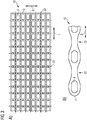
- the glass capillary 2 is a rectangular tube with an elongated, rectangular cross section.
- the sealing areas 22 extend both along the longitudinal axis L and along a transverse axis Q, perpendicular to the longitudinal axis L.
- the sealing areas 22 are symbolized by dashed lines.
- Figure 3B a cross-sectional representation is shown.
- Such a glass capillary 2 enables a two-dimensional arrangement of regions with the phosphor 3 to be implemented.
- Such a two-dimensional arrangement of the areas with the phosphor 3 can be applied to a two-dimensional array of LED chips 4, not shown.
- the conversion element 10 can also be separated along the sealing areas 22, analogously to FIG Figure 2C .
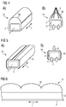
- the glass capillary 2 has an optical element 92.
- the optical element 92 is designed as a converging lens which extends constantly along the longitudinal axis L.
- a side of the glass capillary 2 opposite the lens 92 is designed flat and is set up so that the light-emitting diode chips 4 are attached to it.
- such a lens 92 enables beam shaping, for example of the secondary radiation S, to be achieved.
- an opaque, reflecting or also absorbing coating 91 is applied in places to an outer surface of the glass capillary 2.
- the coating 91 is formed, for example, from one or more metals.
- No coating is applied to the glass capillary 2 on an underside on which the light-emitting diode chips 4 are provided for mounting.
- a region in the form of a strip is left open in order to allow the secondary radiation S and / or residues of the primary radiation P to emerge from the glass capillary 2.
- the coating 91 or the optical element 92 of the Figures 4 and 5 extend uniformly along the longitudinal axis L.
- Figure 6 it is shown in a sectional view that deviates from this that individual lenses or optical elements 92 can also be formed along the longitudinal axis L. The same applies to the coating 91 Figure 5 possible.
- FIG. 7 Further sectional views of conversion elements 10 are shown. To simplify the illustration, only one sealing area 22 is shown at one end of the glass capillary 2. Also related to Figure 7 there may be sealing areas and geometries of the glass capillary 2, as in connection with the Figures 1 to 6 shown, preferably as in connection with the Figures 2 or 3rd explained.
- FIG. 7A is at one end of the glass capillary 2 close to the sealing area 22 a capture material 82, also referred to as a getter. Moisture or oxygen can be removed from the remaining volume of the glass capillary 2 via the capture material 82.
- FIG. 7B there is an indicator material 81 in the glass capillary 2.
- the indicator material 81 shows whether there is oxygen or moisture in the glass capillary 2 and / or whether a permissible, maximum processing temperature was maintained when the sealing area 22 was produced.
- Such an indicator material 81 can also be present in combination with a capture material 82.
- an insulating element 83 can be introduced into the glass capillary 2 near the sealing area 22, see Figure 7C .
- the insulating element 83 is preferably thermally insulating and can be opaque. As a result, the phosphor 3 can be better protected against overheating when the sealing region 22 is produced.
- the insulating element 83 is preferably formed from a solid, alternatively from a liquid, and is preferably introduced into the glass capillary 2 at a distance of at most 1 mm or 0.5 mm from the sealing area 22 or directly at the sealing area 22.
- the insulating element 83 preferably seals the glass capillary 2, so that the insulating element 83 extends over the entire inner region of the glass capillary 2, seen in cross section.
- a specific thermal conductivity of the material of the insulating element 83 is preferably at most 0.5 W / K • m or 0.2 W / K • m or 0.05 W / K • m.
- the phosphors 3a, 3b, 3c with different emission properties are introduced into the glass capillary 2, which follow one another directly along the longitudinal axis L.
- the phosphors 3a, 3b, 3c generate blue, green and red light, for example after excitation with primary radiation from the near ultraviolet spectral range or after excitation with blue light, for example with a dominance wavelength of 450 nm, for example with a tolerance of 5 nm
- the phosphor 3a is in direct contact with the insulating element 83.
- the phosphors 3a, 3b, 3c are spaced apart. Several phosphors are also present in all other exemplary embodiments.
Landscapes
- Physics & Mathematics (AREA)
- Optics & Photonics (AREA)
- Engineering & Computer Science (AREA)
- Manufacturing & Machinery (AREA)
- Led Device Packages (AREA)
Claims (15)
- Un procédé de fabrication de composants semi-conducteurs électroluminescents (1), comprenant les étapes suivantes:A) fournir au moins un capillaire en verre (2) constitué d'un matériau en verre,B) remplir le capillaire de verre (2) avec une pluralité de luminophores (3) différents,C) sceller le capillaire en verre (2) dans une région d'étanchéité (22) par fusion et/ou ramollissement du matériau en verre de telle sorte que le capillaire en verre (2) est fermé par le matériau en verre lui-même, etD) fixer au moins une partie du capillaire de verre scellé (2) à au moins une puce de diode électroluminescente (4) de telle sorte que, pendant le fonctionnement, le rayonnement émis par la puce de diode électroluminescente (4) est partiellement ou complètement converti en lumière d'une longueur d'onde supérieure par les luminophores (3),dans l'étape C), une distance entre la région d'étanchéité (22) et les luminophores (3) est d'au plus 4 mm,
les différents luminophores (3) étant présents séparément les uns des autres le long d'un axe longitudinal (L) du capillaire en verre (2), et
les luminophores (3) sont injectés avec une seringue (5) dans le capillaire de verre (2) de sorte que les zones remplies avec les luminophores (3) et les zones remplies d'un gaz protecteur (6) alternent les unes avec les autres dans le capillaire de verre (2) après l'étape B). - Le procédé selon la revendication précédente,
dans lequel le capillaire en verre (2) a une épaisseur de paroi moyenne d'au moins 20 µm et d'au plus 125 µm avant l'étape C),
une durée de l'étape C) de procédé par région d'étanchéité (22) étant d'au plus 4 s, et
les phosphores (3) sont des points quantiques et/ou des molécules organiques. - Le procédé selon l'une des revendications précédentes,
dans l'étape B), les luminophores (3) sont placés dans un matériau de matrice (32) liquide qui est introduit dans le capillaire de verre (2),
le matériau matrice (32) est ensuite photochimiquement ou thermiquement durci. - Le procédé selon la revendication précédente,
dans laquelle le matériau de matrice (32) à l'étape B) présente un angle de contact (a) sur le capillaire de verre (2) d'au moins 65° et d'au plus 105°,
un quotient d'une longueur du capillaire en verre (2) et d'un diamètre du capillaire en verre (2) est d'au moins 15 et au plus 150. - Le procédé selon l'une des revendications précédentes,
le matériau de verre est un verre de borosilicate perméable à la lumière ayant des fractions de masse d'au moins 70% de dioxyde de silicium et d'au moins 7% de trioxyde de bore,
une température de traitement du matériau de verre dans l'étape C) étant d'au moins 500°C et d'au plus 900°C,
dans l'étape C), le capillaire en verre (2) est retenu sous la forme d'une unité autosupportée mécaniquement, de telle sorte qu'aucune séparation ou fusion n'a lieu à l'étape C). - Le procédé selon l'une quelconque des revendications 1 à 4,
le matériau de verre étant un verre à bas point de fusion et
une température de traitement du matériau de verre dans l'étape C) étant d'au moins 200°C et d'au plus 500°C. - Le procédé selon l'une des revendications précédentes,
dans lequel, avant l'étape C), une aire de section transversale moyenne d'un intérieur du capillaire en verre (2) est d'au moins 0,2 mm x 0,3 mm et d'au plus 1,5 mm x 0,8 mm,
la surface de section transversale est un rectangle ou un rectangle avec des coins arrondis. - Le procédé selon l'une des revendications précédentes,
dans lequel la fusion à l'étape C) a lieu avec au moins un fil chauffant électrique externe (7) situé à l'extérieur du capillaire en verre (2). - Le procédé selon l'une des revendications précédentes,
dans lequel le capillaire en verre (2), vu en coupe transversale, présente une pluralité d'espaces internes adjacents qui sont chacun remplis avec les luminophores (3). - Le procédé selon l'une des revendications précédentes,
dans lequel exactement trois luminophores (3a, 3b, 3c) différents présentant des propriétés d'émission différentes sont introduits dans le capillaire de verre (2),
les luminophores (3a, 3b, 3c) indépendamment les uns des autres génèrent de la lumière bleue, verte et rouge, après excitation avec un rayonnement primaire provenant de la région spectrale proche de l'ultraviolet ou après excitation avec une lumière bleue,
un élément isolant (83) est introduit dans le capillaire de verre (2) à une distance d'au plus 0,5 mm de la zone d'étanchéité (22), et l'élément isolant (83) est thermiquement isolant et opaque de sorte que les luminophores sont protégés contre une surchauffe lorsque la zone d'étanchéité (22) est produite, et
l'un des luminophores étant en contact direct avec l'élément isolant (83). - Le procédé selon l'une des revendications précédentes, comprenant une étape E) dans laquelle le capillaire en verre (2) est séparé en éléments de conversion (10),
l'étape E) suit l'étape C) et/ou l'étape D). - Le procédé selon la revendication précédente,
une pluralité de régions d'étanchéité (22) sont présentes le long de l'axe longitudinal (L) et, dans chaque cas, une partie des luminophores est située entre au moins certaines régions d'étanchéité adjacentes (22),
la séparation à l'étape E) a lieu dans au moins une partie des zones d'étanchéité (22). - Le procédé selon la revendication précédente,
dans lequel une pluralité de régions de séparation (22) sont présentes à la fois le long de la direction longitudinale (L) et le long d'un axe transversal (Q), de telle sorte qu'un agencement bidimensionnel de régions avec les luminophores (3) est présent,
un champ bidimensionnel de puces de diode électroluminescente (4) est appliqué à cet agencement bidimensionnel à l'étape D) . - Le procédé selon l'une des revendications précédentes,
dans l'étape B), au moins un indicateur (81) pour au moins une des variables: la teneur en humidité, la teneur en oxygène et la température maximale et, en variante ou en outre, au moins un matériau de piégeage pour l'oxygène ou l'humidité est introduit dans le capillaire en verre (2). - Le procédé selon l'une des revendications précédentes,
dans lequel un revêtement réfléchissant opaque (91) est appliqué à l'extérieur du capillaire en verre (2) et/ou dans lequel le capillaire en verre (2) est formé au moins par endroits sous la forme d'un élément optique (92).
Applications Claiming Priority (2)
| Application Number | Priority Date | Filing Date | Title |
|---|---|---|---|
| DE102015114175.2A DE102015114175A1 (de) | 2015-08-26 | 2015-08-26 | Verfahren zur Herstellung von lichtemittierenden Halbleiterbauteilen und lichtemittierendes Halbleiterbauteil |
| PCT/EP2016/069069 WO2017032605A1 (fr) | 2015-08-26 | 2016-08-10 | Procédé de fabrication de composants semiconducteurs électroluminescents et composant semiconducteur électroluminescent |
Publications (2)
| Publication Number | Publication Date |
|---|---|
| EP3341975A1 EP3341975A1 (fr) | 2018-07-04 |
| EP3341975B1 true EP3341975B1 (fr) | 2020-06-03 |
Family
ID=56741038
Family Applications (1)
| Application Number | Title | Priority Date | Filing Date |
|---|---|---|---|
| EP16754243.0A Active EP3341975B1 (fr) | 2015-08-26 | 2016-08-10 | Procédé de fabrication de composants semiconducteurs électroluminescents |
Country Status (4)
| Country | Link |
|---|---|
| US (1) | US20200083401A1 (fr) |
| EP (1) | EP3341975B1 (fr) |
| DE (1) | DE102015114175A1 (fr) |
| WO (1) | WO2017032605A1 (fr) |
Families Citing this family (2)
| Publication number | Priority date | Publication date | Assignee | Title |
|---|---|---|---|---|
| DE102017121480B4 (de) * | 2017-09-15 | 2024-04-18 | OSRAM Opto Semiconductors Gesellschaft mit beschränkter Haftung | Lichtemittierendes Halbleiterbauteil |
| EP4166843B1 (fr) | 2021-10-18 | 2024-04-03 | Volkswagen Ag | Dispositif d'éclairage pour un véhicule automobile |
Citations (1)
| Publication number | Priority date | Publication date | Assignee | Title |
|---|---|---|---|---|
| WO2013015532A2 (fr) * | 2011-07-27 | 2013-01-31 | Lg Innotek Co., Ltd. | Élément optique, dispositif d'affichage et dispositif d'émission de lumière le comprenant |
Family Cites Families (11)
| Publication number | Priority date | Publication date | Assignee | Title |
|---|---|---|---|---|
| US20100110728A1 (en) * | 2007-03-19 | 2010-05-06 | Nanosys, Inc. | Light-emitting diode (led) devices comprising nanocrystals |
| US20100155749A1 (en) * | 2007-03-19 | 2010-06-24 | Nanosys, Inc. | Light-emitting diode (led) devices comprising nanocrystals |
| EP2370993A1 (fr) * | 2008-12-30 | 2011-10-05 | Nanosys, Inc. | Procédés d'encapsulation de nanocristaux et compositions résultantes |
| JP2013509714A (ja) * | 2009-10-30 | 2013-03-14 | ナノシス・インク. | ナノ結晶を含む発光ダイオード(led)デバイス |
| KR101261461B1 (ko) * | 2010-07-14 | 2013-05-10 | 엘지이노텍 주식회사 | 액정 표시 장치 |
| CN103025670B (zh) * | 2010-07-28 | 2016-08-10 | 日本电气硝子株式会社 | 荧光体封入用毛细管的制造方法、荧光体封入用毛细管、波长变换部件和波长变换部件的制造方法 |
| DE112011104781T5 (de) * | 2011-01-26 | 2013-10-31 | Fraunhofer-Gesellschaft zur Förderung der angewandten Forschung e.V. | Photovoltaik-Konzentrator-Empfänger und seine Verwendung |
| US9864121B2 (en) * | 2011-11-22 | 2018-01-09 | Samsung Electronics Co., Ltd. | Stress-resistant component for use with quantum dots |
| JP5939004B2 (ja) * | 2012-04-11 | 2016-06-22 | ソニー株式会社 | 発光装置、表示装置および照明装置 |
| DE102012103393A1 (de) | 2012-04-18 | 2013-10-24 | Osram Opto Semiconductors Gmbh | Transparenter Körper, optoelektronisches Bauelement mit einem transparenten Körper und Verfahren zur Herstellung eines transparenten Körpers |
| EP3058401A4 (fr) * | 2013-10-17 | 2017-05-17 | Nanosys, Inc. | Dispositifs à diodes électroluminescentes (del) |
-
2015
- 2015-08-26 DE DE102015114175.2A patent/DE102015114175A1/de not_active Withdrawn
-
2016
- 2016-08-10 WO PCT/EP2016/069069 patent/WO2017032605A1/fr not_active Ceased
- 2016-08-10 EP EP16754243.0A patent/EP3341975B1/fr active Active
- 2016-08-10 US US15/749,768 patent/US20200083401A1/en not_active Abandoned
Patent Citations (1)
| Publication number | Priority date | Publication date | Assignee | Title |
|---|---|---|---|---|
| WO2013015532A2 (fr) * | 2011-07-27 | 2013-01-31 | Lg Innotek Co., Ltd. | Élément optique, dispositif d'affichage et dispositif d'émission de lumière le comprenant |
Also Published As
| Publication number | Publication date |
|---|---|
| US20200083401A1 (en) | 2020-03-12 |
| EP3341975A1 (fr) | 2018-07-04 |
| WO2017032605A1 (fr) | 2017-03-02 |
| DE102015114175A1 (de) | 2017-03-16 |
Similar Documents
| Publication | Publication Date | Title |
|---|---|---|
| DE102010009456A1 (de) | Strahlungsemittierendes Bauelement mit einem Halbleiterchip und einem Konversionselement und Verfahren zu dessen Herstellung | |
| DE102014108368A1 (de) | Oberflächenmontierbares Halbleiterbauelement und Verfahren zu dessen Herstellung | |
| WO2011012371A1 (fr) | Procédé de fabrication dun élément comportant au moins un matériau organique et élément comportant au moins un matériau organique | |
| DE102008063636A1 (de) | Verfahren zur Herstellung eines organischen optoelektronischen Bauelements und organisches optoelektronisches Bauelement | |
| WO2009039816A1 (fr) | Élément rayonnant doté d'un couvercle de verre et procédé de fabrication | |
| DE102014116778A1 (de) | Verfahren zur Herstellung eines Konversionselements, Konversionselement sowie optoelektronisches Bauelement mit einem solchen Konversionselement | |
| EP3341975B1 (fr) | Procédé de fabrication de composants semiconducteurs électroluminescents | |
| DE112018004215B4 (de) | Herstellung einer Halbleitervorrichtung und Halbleitervorrichtung | |
| WO2013041313A1 (fr) | Plaquette de conversion, composant émettant un rayonnement équipé d'une telle plaquette de conversion, et procédé de fabrication d'une telle plaquette de conversion | |
| WO2024125914A1 (fr) | Composant optoélectronique et procédé de fabrication d'un composant optoélectronique | |
| DE112014002023B4 (de) | Optoelektronisches Bauelement und Verfahren zu seiner Herstellung | |
| EP3064166B1 (fr) | Éclairage del etancheifie et procede de fabrication d'un eclairage del etancheifie | |
| WO2016087444A1 (fr) | Composant semi-conducteur optoélectronique émetteur de rayonnements et son procédé de fabrication | |
| DE102015116263A1 (de) | Herstellung eines elektronischen Bauelements | |
| EP3275022B1 (fr) | Module optoélectronique et procédé de manufacture d'un module optoélectronique | |
| EP2460203B1 (fr) | Élément organique et son procédé de fabrication | |
| DE102005010311A1 (de) | Verfahren und Gießform zur Herstellung eines optischen Halbleitermoduls | |
| DE102015103331A1 (de) | Hermetisch abgedichtete LED-Leuchte, Verfahren zur Herstellung einer hermetisch abgedichteten LED-Leuchte sowie ärztliches Instrument umfassend eine hermetisch abgedichtete LED-Leuchte | |
| DE102008021676A1 (de) | Bauteil mit einem ersten und einem zweiten Substrat und Verfahren zu dessen Herstellung | |
| DE202010000518U1 (de) | Lampe mit einer in einem hermetisch verschlossenen Gehäuse angeordneten LED | |
| DE102014111483A1 (de) | Herstellung eines optoelektronischen Bauelements und optoelektronisches Bauelement | |
| DE102023131804A1 (de) | Optoelektronisches bauelement und verfahren zu dessen herstellung | |
| WO2019101745A1 (fr) | Dispositif comprenant un cadre conducteur et procédé servant à fabriquer une pluralité de dispositifs | |
| DE102008035538B4 (de) | Bauteil mit mindestens einem organischen Material und Verfahren zu dessen Herstellung | |
| DE102008033394B4 (de) | Bauteil mit einem ersten und einem zweiten Substrat |
Legal Events
| Date | Code | Title | Description |
|---|---|---|---|
| STAA | Information on the status of an ep patent application or granted ep patent |
Free format text: STATUS: THE INTERNATIONAL PUBLICATION HAS BEEN MADE |
|
| PUAI | Public reference made under article 153(3) epc to a published international application that has entered the european phase |
Free format text: ORIGINAL CODE: 0009012 |
|
| STAA | Information on the status of an ep patent application or granted ep patent |
Free format text: STATUS: REQUEST FOR EXAMINATION WAS MADE |
|
| 17P | Request for examination filed |
Effective date: 20180108 |
|
| AK | Designated contracting states |
Kind code of ref document: A1 Designated state(s): AL AT BE BG CH CY CZ DE DK EE ES FI FR GB GR HR HU IE IS IT LI LT LU LV MC MK MT NL NO PL PT RO RS SE SI SK SM TR |
|
| AX | Request for extension of the european patent |
Extension state: BA ME |
|
| RIN1 | Information on inventor provided before grant (corrected) |
Inventor name: GOEOETZ, BRITTA Inventor name: O'BRIEN, DAVID Inventor name: VON MALM, NORWIN |
|
| DAV | Request for validation of the european patent (deleted) | ||
| DAX | Request for extension of the european patent (deleted) | ||
| RAP1 | Party data changed (applicant data changed or rights of an application transferred) |
Owner name: OSRAM OPTO SEMICONDUCTORS GMBH |
|
| REG | Reference to a national code |
Ref country code: DE Ref legal event code: R079 Ref document number: 502016010129 Country of ref document: DE Free format text: PREVIOUS MAIN CLASS: H01L0033500000 Ipc: H01L0033000000 |
|
| GRAP | Despatch of communication of intention to grant a patent |
Free format text: ORIGINAL CODE: EPIDOSNIGR1 |
|
| STAA | Information on the status of an ep patent application or granted ep patent |
Free format text: STATUS: GRANT OF PATENT IS INTENDED |
|
| RIC1 | Information provided on ipc code assigned before grant |
Ipc: H01L 33/50 20100101ALI20200309BHEP Ipc: H01L 33/00 20100101AFI20200309BHEP |
|
| INTG | Intention to grant announced |
Effective date: 20200324 |
|
| GRAS | Grant fee paid |
Free format text: ORIGINAL CODE: EPIDOSNIGR3 |
|
| GRAA | (expected) grant |
Free format text: ORIGINAL CODE: 0009210 |
|
| STAA | Information on the status of an ep patent application or granted ep patent |
Free format text: STATUS: THE PATENT HAS BEEN GRANTED |
|
| AK | Designated contracting states |
Kind code of ref document: B1 Designated state(s): AL AT BE BG CH CY CZ DE DK EE ES FI FR GB GR HR HU IE IS IT LI LT LU LV MC MK MT NL NO PL PT RO RS SE SI SK SM TR |
|
| REG | Reference to a national code |
Ref country code: GB Ref legal event code: FG4D Free format text: NOT ENGLISH |
|
| REG | Reference to a national code |
Ref country code: CH Ref legal event code: EP Ref country code: AT Ref legal event code: REF Ref document number: 1277934 Country of ref document: AT Kind code of ref document: T Effective date: 20200615 |
|
| REG | Reference to a national code |
Ref country code: DE Ref legal event code: R096 Ref document number: 502016010129 Country of ref document: DE |
|
| REG | Reference to a national code |
Ref country code: LT Ref legal event code: MG4D |
|
| PG25 | Lapsed in a contracting state [announced via postgrant information from national office to epo] |
Ref country code: SE Free format text: LAPSE BECAUSE OF FAILURE TO SUBMIT A TRANSLATION OF THE DESCRIPTION OR TO PAY THE FEE WITHIN THE PRESCRIBED TIME-LIMIT Effective date: 20200603 Ref country code: LT Free format text: LAPSE BECAUSE OF FAILURE TO SUBMIT A TRANSLATION OF THE DESCRIPTION OR TO PAY THE FEE WITHIN THE PRESCRIBED TIME-LIMIT Effective date: 20200603 Ref country code: FI Free format text: LAPSE BECAUSE OF FAILURE TO SUBMIT A TRANSLATION OF THE DESCRIPTION OR TO PAY THE FEE WITHIN THE PRESCRIBED TIME-LIMIT Effective date: 20200603 Ref country code: NO Free format text: LAPSE BECAUSE OF FAILURE TO SUBMIT A TRANSLATION OF THE DESCRIPTION OR TO PAY THE FEE WITHIN THE PRESCRIBED TIME-LIMIT Effective date: 20200903 Ref country code: GR Free format text: LAPSE BECAUSE OF FAILURE TO SUBMIT A TRANSLATION OF THE DESCRIPTION OR TO PAY THE FEE WITHIN THE PRESCRIBED TIME-LIMIT Effective date: 20200904 |
|
| REG | Reference to a national code |
Ref country code: NL Ref legal event code: MP Effective date: 20200603 |
|
| PG25 | Lapsed in a contracting state [announced via postgrant information from national office to epo] |
Ref country code: BG Free format text: LAPSE BECAUSE OF FAILURE TO SUBMIT A TRANSLATION OF THE DESCRIPTION OR TO PAY THE FEE WITHIN THE PRESCRIBED TIME-LIMIT Effective date: 20200903 Ref country code: RS Free format text: LAPSE BECAUSE OF FAILURE TO SUBMIT A TRANSLATION OF THE DESCRIPTION OR TO PAY THE FEE WITHIN THE PRESCRIBED TIME-LIMIT Effective date: 20200603 Ref country code: HR Free format text: LAPSE BECAUSE OF FAILURE TO SUBMIT A TRANSLATION OF THE DESCRIPTION OR TO PAY THE FEE WITHIN THE PRESCRIBED TIME-LIMIT Effective date: 20200603 Ref country code: LV Free format text: LAPSE BECAUSE OF FAILURE TO SUBMIT A TRANSLATION OF THE DESCRIPTION OR TO PAY THE FEE WITHIN THE PRESCRIBED TIME-LIMIT Effective date: 20200603 |
|
| PG25 | Lapsed in a contracting state [announced via postgrant information from national office to epo] |
Ref country code: NL Free format text: LAPSE BECAUSE OF FAILURE TO SUBMIT A TRANSLATION OF THE DESCRIPTION OR TO PAY THE FEE WITHIN THE PRESCRIBED TIME-LIMIT Effective date: 20200603 Ref country code: AL Free format text: LAPSE BECAUSE OF FAILURE TO SUBMIT A TRANSLATION OF THE DESCRIPTION OR TO PAY THE FEE WITHIN THE PRESCRIBED TIME-LIMIT Effective date: 20200603 |
|
| PG25 | Lapsed in a contracting state [announced via postgrant information from national office to epo] |
Ref country code: PT Free format text: LAPSE BECAUSE OF FAILURE TO SUBMIT A TRANSLATION OF THE DESCRIPTION OR TO PAY THE FEE WITHIN THE PRESCRIBED TIME-LIMIT Effective date: 20201006 Ref country code: IT Free format text: LAPSE BECAUSE OF FAILURE TO SUBMIT A TRANSLATION OF THE DESCRIPTION OR TO PAY THE FEE WITHIN THE PRESCRIBED TIME-LIMIT Effective date: 20200603 Ref country code: EE Free format text: LAPSE BECAUSE OF FAILURE TO SUBMIT A TRANSLATION OF THE DESCRIPTION OR TO PAY THE FEE WITHIN THE PRESCRIBED TIME-LIMIT Effective date: 20200603 Ref country code: SM Free format text: LAPSE BECAUSE OF FAILURE TO SUBMIT A TRANSLATION OF THE DESCRIPTION OR TO PAY THE FEE WITHIN THE PRESCRIBED TIME-LIMIT Effective date: 20200603 Ref country code: CZ Free format text: LAPSE BECAUSE OF FAILURE TO SUBMIT A TRANSLATION OF THE DESCRIPTION OR TO PAY THE FEE WITHIN THE PRESCRIBED TIME-LIMIT Effective date: 20200603 Ref country code: RO Free format text: LAPSE BECAUSE OF FAILURE TO SUBMIT A TRANSLATION OF THE DESCRIPTION OR TO PAY THE FEE WITHIN THE PRESCRIBED TIME-LIMIT Effective date: 20200603 Ref country code: ES Free format text: LAPSE BECAUSE OF FAILURE TO SUBMIT A TRANSLATION OF THE DESCRIPTION OR TO PAY THE FEE WITHIN THE PRESCRIBED TIME-LIMIT Effective date: 20200603 |
|
| PG25 | Lapsed in a contracting state [announced via postgrant information from national office to epo] |
Ref country code: SK Free format text: LAPSE BECAUSE OF FAILURE TO SUBMIT A TRANSLATION OF THE DESCRIPTION OR TO PAY THE FEE WITHIN THE PRESCRIBED TIME-LIMIT Effective date: 20200603 Ref country code: PL Free format text: LAPSE BECAUSE OF FAILURE TO SUBMIT A TRANSLATION OF THE DESCRIPTION OR TO PAY THE FEE WITHIN THE PRESCRIBED TIME-LIMIT Effective date: 20200603 Ref country code: IS Free format text: LAPSE BECAUSE OF FAILURE TO SUBMIT A TRANSLATION OF THE DESCRIPTION OR TO PAY THE FEE WITHIN THE PRESCRIBED TIME-LIMIT Effective date: 20201003 |
|
| REG | Reference to a national code |
Ref country code: DE Ref legal event code: R097 Ref document number: 502016010129 Country of ref document: DE |
|
| PG25 | Lapsed in a contracting state [announced via postgrant information from national office to epo] |
Ref country code: MC Free format text: LAPSE BECAUSE OF FAILURE TO SUBMIT A TRANSLATION OF THE DESCRIPTION OR TO PAY THE FEE WITHIN THE PRESCRIBED TIME-LIMIT Effective date: 20200603 |
|
| REG | Reference to a national code |
Ref country code: CH Ref legal event code: PL |
|
| PLBE | No opposition filed within time limit |
Free format text: ORIGINAL CODE: 0009261 |
|
| STAA | Information on the status of an ep patent application or granted ep patent |
Free format text: STATUS: NO OPPOSITION FILED WITHIN TIME LIMIT |
|
| PG25 | Lapsed in a contracting state [announced via postgrant information from national office to epo] |
Ref country code: DK Free format text: LAPSE BECAUSE OF FAILURE TO SUBMIT A TRANSLATION OF THE DESCRIPTION OR TO PAY THE FEE WITHIN THE PRESCRIBED TIME-LIMIT Effective date: 20200603 Ref country code: CH Free format text: LAPSE BECAUSE OF NON-PAYMENT OF DUE FEES Effective date: 20200831 Ref country code: LU Free format text: LAPSE BECAUSE OF NON-PAYMENT OF DUE FEES Effective date: 20200810 Ref country code: LI Free format text: LAPSE BECAUSE OF NON-PAYMENT OF DUE FEES Effective date: 20200831 |
|
| 26N | No opposition filed |
Effective date: 20210304 |
|
| GBPC | Gb: european patent ceased through non-payment of renewal fee |
Effective date: 20200903 |
|
| REG | Reference to a national code |
Ref country code: BE Ref legal event code: MM Effective date: 20200831 |
|
| PG25 | Lapsed in a contracting state [announced via postgrant information from national office to epo] |
Ref country code: SI Free format text: LAPSE BECAUSE OF FAILURE TO SUBMIT A TRANSLATION OF THE DESCRIPTION OR TO PAY THE FEE WITHIN THE PRESCRIBED TIME-LIMIT Effective date: 20200603 |
|
| PG25 | Lapsed in a contracting state [announced via postgrant information from national office to epo] |
Ref country code: FR Free format text: LAPSE BECAUSE OF NON-PAYMENT OF DUE FEES Effective date: 20200831 |
|
| PG25 | Lapsed in a contracting state [announced via postgrant information from national office to epo] |
Ref country code: GB Free format text: LAPSE BECAUSE OF NON-PAYMENT OF DUE FEES Effective date: 20200903 Ref country code: IE Free format text: LAPSE BECAUSE OF NON-PAYMENT OF DUE FEES Effective date: 20200810 Ref country code: BE Free format text: LAPSE BECAUSE OF NON-PAYMENT OF DUE FEES Effective date: 20200831 |
|
| PG25 | Lapsed in a contracting state [announced via postgrant information from national office to epo] |
Ref country code: TR Free format text: LAPSE BECAUSE OF FAILURE TO SUBMIT A TRANSLATION OF THE DESCRIPTION OR TO PAY THE FEE WITHIN THE PRESCRIBED TIME-LIMIT Effective date: 20200603 Ref country code: MT Free format text: LAPSE BECAUSE OF FAILURE TO SUBMIT A TRANSLATION OF THE DESCRIPTION OR TO PAY THE FEE WITHIN THE PRESCRIBED TIME-LIMIT Effective date: 20200603 Ref country code: CY Free format text: LAPSE BECAUSE OF FAILURE TO SUBMIT A TRANSLATION OF THE DESCRIPTION OR TO PAY THE FEE WITHIN THE PRESCRIBED TIME-LIMIT Effective date: 20200603 |
|
| PG25 | Lapsed in a contracting state [announced via postgrant information from national office to epo] |
Ref country code: MK Free format text: LAPSE BECAUSE OF FAILURE TO SUBMIT A TRANSLATION OF THE DESCRIPTION OR TO PAY THE FEE WITHIN THE PRESCRIBED TIME-LIMIT Effective date: 20200603 |
|
| REG | Reference to a national code |
Ref country code: AT Ref legal event code: MM01 Ref document number: 1277934 Country of ref document: AT Kind code of ref document: T Effective date: 20210810 |
|
| PG25 | Lapsed in a contracting state [announced via postgrant information from national office to epo] |
Ref country code: AT Free format text: LAPSE BECAUSE OF NON-PAYMENT OF DUE FEES Effective date: 20210810 |
|
| P01 | Opt-out of the competence of the unified patent court (upc) registered |
Effective date: 20230825 |
|
| REG | Reference to a national code |
Ref country code: DE Ref legal event code: R079 Ref document number: 502016010129 Country of ref document: DE Free format text: PREVIOUS MAIN CLASS: H01L0033000000 Ipc: H10H0020000000 |
|
| PGFP | Annual fee paid to national office [announced via postgrant information from national office to epo] |
Ref country code: DE Payment date: 20250820 Year of fee payment: 10 |