EP3342003B1 - Monolithic phased-array antenna system - Google Patents
Monolithic phased-array antenna system Download PDFInfo
- Publication number
- EP3342003B1 EP3342003B1 EP16754100.2A EP16754100A EP3342003B1 EP 3342003 B1 EP3342003 B1 EP 3342003B1 EP 16754100 A EP16754100 A EP 16754100A EP 3342003 B1 EP3342003 B1 EP 3342003B1
- Authority
- EP
- European Patent Office
- Prior art keywords
- antenna
- transformer elements
- antenna transformer
- phased
- array
- Prior art date
- Legal status (The legal status is an assumption and is not a legal conclusion. Google has not performed a legal analysis and makes no representation as to the accuracy of the status listed.)
- Active
Links
Images


Classifications
-
- H—ELECTRICITY
- H01—ELECTRIC ELEMENTS
- H01Q—ANTENNAS, i.e. RADIO AERIALS
- H01Q3/00—Arrangements for changing or varying the orientation or the shape of the directional pattern of the waves radiated from an antenna or antenna system
- H01Q3/26—Arrangements for changing or varying the orientation or the shape of the directional pattern of the waves radiated from an antenna or antenna system varying the relative phase or relative amplitude of energisation between two or more active radiating elements; varying the distribution of energy across a radiating aperture
-
- B—PERFORMING OPERATIONS; TRANSPORTING
- B33—ADDITIVE MANUFACTURING TECHNOLOGY
- B33Y—ADDITIVE MANUFACTURING, i.e. MANUFACTURING OF THREE-DIMENSIONAL [3D] OBJECTS BY ADDITIVE DEPOSITION, ADDITIVE AGGLOMERATION OR ADDITIVE LAYERING, e.g. BY 3D PRINTING, STEREOLITHOGRAPHY OR SELECTIVE LASER SINTERING
- B33Y10/00—Processes of additive manufacturing
-
- B—PERFORMING OPERATIONS; TRANSPORTING
- B33—ADDITIVE MANUFACTURING TECHNOLOGY
- B33Y—ADDITIVE MANUFACTURING, i.e. MANUFACTURING OF THREE-DIMENSIONAL [3D] OBJECTS BY ADDITIVE DEPOSITION, ADDITIVE AGGLOMERATION OR ADDITIVE LAYERING, e.g. BY 3D PRINTING, STEREOLITHOGRAPHY OR SELECTIVE LASER SINTERING
- B33Y50/00—Data acquisition or data processing for additive manufacturing
- B33Y50/02—Data acquisition or data processing for additive manufacturing for controlling or regulating additive manufacturing processes
-
- B—PERFORMING OPERATIONS; TRANSPORTING
- B33—ADDITIVE MANUFACTURING TECHNOLOGY
- B33Y—ADDITIVE MANUFACTURING, i.e. MANUFACTURING OF THREE-DIMENSIONAL [3D] OBJECTS BY ADDITIVE DEPOSITION, ADDITIVE AGGLOMERATION OR ADDITIVE LAYERING, e.g. BY 3D PRINTING, STEREOLITHOGRAPHY OR SELECTIVE LASER SINTERING
- B33Y80/00—Products made by additive manufacturing
-
- H—ELECTRICITY
- H01—ELECTRIC ELEMENTS
- H01Q—ANTENNAS, i.e. RADIO AERIALS
- H01Q1/00—Details of, or arrangements associated with, antennas
- H01Q1/50—Structural association of antennas with earthing switches, lead-in devices or lightning protectors
-
- H—ELECTRICITY
- H01—ELECTRIC ELEMENTS
- H01Q—ANTENNAS, i.e. RADIO AERIALS
- H01Q13/00—Waveguide horns or mouths; Slot antennas; Leaky-waveguide antennas; Equivalent structures causing radiation along the transmission path of a guided wave
- H01Q13/08—Radiating ends of two-conductor microwave transmission lines, e.g. of coaxial lines, of microstrip lines
- H01Q13/085—Slot-line radiating ends
-
- H—ELECTRICITY
- H01—ELECTRIC ELEMENTS
- H01Q—ANTENNAS, i.e. RADIO AERIALS
- H01Q21/00—Antenna arrays or systems
- H01Q21/0087—Apparatus or processes specially adapted for manufacturing antenna arrays
-
- H—ELECTRICITY
- H01—ELECTRIC ELEMENTS
- H01Q—ANTENNAS, i.e. RADIO AERIALS
- H01Q21/00—Antenna arrays or systems
- H01Q21/0087—Apparatus or processes specially adapted for manufacturing antenna arrays
- H01Q21/0093—Monolithic arrays
-
- H—ELECTRICITY
- H01—ELECTRIC ELEMENTS
- H01Q—ANTENNAS, i.e. RADIO AERIALS
- H01Q21/00—Antenna arrays or systems
- H01Q21/06—Arrays of individually energised antenna units similarly polarised and spaced apart
- H01Q21/061—Two dimensional planar arrays
- H01Q21/064—Two dimensional planar arrays using horn or slot aerials
-
- H—ELECTRICITY
- H01—ELECTRIC ELEMENTS
- H01Q—ANTENNAS, i.e. RADIO AERIALS
- H01Q21/00—Antenna arrays or systems
- H01Q21/06—Arrays of individually energised antenna units similarly polarised and spaced apart
- H01Q21/061—Two dimensional planar arrays
- H01Q21/067—Two dimensional planar arrays using endfire radiating aerial units transverse to the plane of the array
-
- H—ELECTRICITY
- H01—ELECTRIC ELEMENTS
- H01Q—ANTENNAS, i.e. RADIO AERIALS
- H01Q21/00—Antenna arrays or systems
- H01Q21/24—Combinations of antenna units polarised in different directions for transmitting or receiving circularly and elliptically polarised waves or waves linearly polarised in any direction
-
- H—ELECTRICITY
- H01—ELECTRIC ELEMENTS
- H01Q—ANTENNAS, i.e. RADIO AERIALS
- H01Q21/00—Antenna arrays or systems
- H01Q21/29—Combinations of different interacting antenna units for giving a desired directional characteristic
- H01Q21/293—Combinations of different interacting antenna units for giving a desired directional characteristic one unit or more being an array of identical aerial elements
Definitions
- the present invention relates generally to communications, and specifically to a monolithic phased-array antenna system.
- Antennas are implemented for a variety of purposes to convert energy from electrical signals to waves propagating in free-space, and thus to transmit and receive wireless signals.
- Antennas can be manufactured in a variety of ways, and for a variety of applications.
- One type of antenna is a phased-array antenna.
- a phased-array antenna includes an array of antennas in which the relative phases of respective signals feeding the antennas are set in such a way that an effective radiation pattern of the array is reinforced in a desired direction and suppressed in undesired directions.
- the array arrangement of the antennas can be such to determine a direction of a received signal based on an order in which the received signal is received at each respective one of the antennas.
- the phase relationships among the antennas in a phased-array antenna may be fixed, such as in a tower array, or may be adjustable, as for beam steering.
- phased-array antennas can be useful for a variety of wireless communications applications.
- US2004/004580 discloses an antenna array that comprises a plurality of antenna elements for creating a plurality of radio frequency waves.
- US 2005/285808 discloses an electrically controlled group antenna including an antenna element suitable for incorporation in such a group antenna and an antenna module including several such antenna elements.
- the antenna elements include a rotationally-symmetrical body tapering towards one end of the body.
- the rotationally-symmetrical body is provided with a metallic casing surface.
- Several antenna elements are arranged separately on a common earth plane.
- a broadband group antenna is achieved that, among other things, is simple in design and is easy to manufacture and repair.
- US 8,736,505 discloses a dual-polarized antenna array.
- the antenna array includes a plurality of self supporting, electrically conductive members. Tapered elements of neighboring electrically conductive members define tapered slots that form part of radiating structures.
- the radiating structures additionally include a slot line in communication with the tapered slot.
- a back cavity can be included as part of a BALUN structure that is integral to an electrically conductive member.
- the system includes a ground plane that is formed from a unitary conductive material.
- the system also includes a plurality of antenna transformer elements that are each formed from the unitary conductive material in an array on a first surface of the ground plane, and being configured to wirelessly transmit or receive a signal.
- the system further includes a plurality of connectors that are each formed from the unitary conductive material on a second surface of the ground plane opposite the first surface. The connectors can be configured to propagate respective portions of the signal to or from the antenna transformer elements.
- the unitary conductive material can be contiguous such that the phased-array antenna system is formed as a monolithic structure to provide conductive coupling of the ground plane, the antenna transformer elements, and the connectors with respect to each other.
- phased-array antenna system includes loading dimensional data regarding the phased-array antenna system into an additive manufacturing machine configured to form the phased-array antenna system.
- the method also includes forming the phased-array antenna system as a monolithic structure of a unitary conductive material via the additive manufacturing machine.
- the phased-array antenna system can include a ground plane, an array of antenna transformer elements disposed on a first surface of the ground plane, and a plurality of connectors formed on a second surface of the ground plane opposite the first surface.
- the plurality of connectors can be configured to propagate respective portions of the signal to or from respective antenna transformer elements of the array of antenna transformer elements.
- the system includes a ground plane and a plurality of antenna transformer elements formed in an array and conductively coupled to a first surface of the ground plane.
- Each of the plurality of antenna transformer elements can be dimensioned to form a balun cavity between respective pairs of the plurality of antenna transformer elements with respect to the ground plane and to form a transformer gap between respective pairs of the plurality of antenna transformer elements to provide impedance matching to free-space.
- the system includes a plurality of connectors formed and conductively coupled to a second surface of the ground plane opposite the first surface, the plurality of connectors being configured to propagate radio frequency signals to or from respective ones of the plurality of antenna transformer elements.
- the system also includes a plurality of coaxial connections between the plurality of connectors and the plurality of transformer elements.
- Each of the plurality of connectors can be associated with one of the plurality of antenna transformer elements and comprising a signal conductor that is formed from the unitary conductive material as an inner conductor of a respective one of the plurality of coaxial connections and extending through an associated one of the plurality of antenna transformer elements that corresponds to an outer conductor of the respective one of the plurality of coaxial connections to an adjacent one of the plurality of antenna transformer elements.
- the phased-array antenna system is formed as a monolithic structure of a unitary conductive material.
- the present invention relates generally to communications, and specifically to a monolithic phased-array antenna system.
- the monolithic phased-array antenna system can be formed as a single structure that can be either metal or a dielectric that is later metalized.
- the monolithic phased-array antenna system can be applicable for broadband operation in a multitude of wireless communications and radar applications.
- the monolithic phased-array antenna system can be composed of an array of transformer elements that are all monolithically fabricated, such as by additive manufacturing (e.g., three-dimensional printing) of antenna transformer elements on a ground plane that forms balun cavities with respect to the transformer elements.
- the phased-array antenna system can also include connectors that are formed on the ground plane beneath the antenna transformer elements, and can each include signal conductors to propagate a communications signal.
- the phased-array antenna system can be formed from a unitary conductive material, and thus can be completely contiguously conductively coupled (e.g., to a DC ground).
- the phased-array antenna system can omit the use of a printed circuit board (PCB) that incorporates a stripline and balun member to convert and excite the respective signal from a given connector to the antenna radiating elements.
- PCB printed circuit board
- Each of the antenna transformer elements can be fabricated with specific dimensions to facilitate specific wave parameters for generating a given signal for communication and/or radar applications. Additionally, each of the connectors that is associated with one of the antenna transformer elements is conductively coupled to at least one adjacent antenna transformer element in a coaxial manner.
- a signal conductor can be coupled to a respective one of the connectors and can extend from beneath an associated one of the antenna transformer elements as an inner conductor of a coaxial connection, through a side portion of the associated one of the antenna transformer elements that forms the outer conductor of the coaxial connection, to an adjacent one of the antenna transformer elements to make a conductive coupling to the exterior of the adjacent antenna transformer element.
- the coaxial arrangement of the connections of each of the connectors through an associated antenna transformer element to a respective adjacent antenna transformer element can be provided in both of two orthogonal directions, such that the orthogonal directions form polarization components of the signal that propagates via the antenna transformer elements.
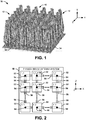
- FIG. 1 illustrates an example of a phased-array antenna system 10.
- the phased-array antenna system 10 can be implemented in a variety of wireless communication and/or radar applications.
- the phased-array antenna system 10 includes a ground plane 12 on which a plurality of antenna transformer elements 14 are formed in an array, demonstrated in an XZ-array in the example of FIG. 1 .
- the antenna transformer elements 14 are formed on a first side of the ground plane 12, and can be associated with a plurality of connectors (not shown) that are formed on a second side of the ground plane 12 opposite the first side.
- the connectors can be configured to propagate an electric signal that can be associated with a wireless signal that is transmitted from or received at the phased-array antenna system 10.
- the connectors can be coupled to the antenna transformer elements 14 in a coaxial connection to provide excitation of the antenna transformer elements 14 to receive or transmit signals from or to the phased-array antenna system 10.
- the phased-array antenna system 10 can be fabricated as a monolithic structure.
- the phased-array antenna system 10 can be formed from an additive manufacturing process (e.g., three-dimensional printing), such that the ground plane 12, the antenna transformer elements 14, and the connectors can all be formed from a unitary conductive material.
- the ground plane 12, the antenna transformer elements 14, and the connectors can be formed from the unitary conductive material via the additive manufacturing process.
- the ground plane 12, the antenna transformer elements 14, and the connectors can be formed from a dielectric material via the additive manufacturing process, and can be metalized to coat the ground plane 12, the antenna transformer elements 14, and the connectors, and thus the entire phased-array antenna system 10, in the unitary conductive material.
- the monolithic arrangement of the phased-array antenna system 10 can be fabricated from other processes, such as compression molding, injection molding, or formed in any other desired manner, such as by using bulk molding or sheet molding compounds or thermoplastic prepreg composite components and structures.
- the monolithic arrangement of the phased-array antenna system 10 can be such that the ground plane 12, the antenna transformer elements 14, and the connectors can all be conductively coupled with respect to each other.
- the monolithic arrangement of the ground plane 12 with respect to the antenna transformer elements 14 can be such that the antenna transformer elements 14 can form baluns with respect to the ground plane 12.
- the phased-array antenna system 10 can omit the use of a printed circuit board (PCB) that incorporates a stripline and balun member to convert and excite the respective signal from a given connector to the antenna radiating elements 14, as opposed to typical phased-array antenna systems.
- PCB printed circuit board
- FIG. 2 illustrates an example diagram of a phased-array antenna system 50.
- the phased-array antenna system 50 can correspond to the phased-array antenna system 10 in the example of FIG. 1 .
- the phased-array antenna system 50 demonstrates a plurality of antenna transformer elements 52 arranged in an XZ-array.
- the phased-array antenna system 50 includes X rows and Y columns of antenna transformer elements 52, with each of the antenna transformer elements 52 being designated by a "row_column" naming convention.
- the phased-array antenna system 10 in the example of FIG. 1 demonstrates a 6x6 array of thirty-six antenna transformer elements 14, the phased-array antenna system 50 can include any XxY arrangement of antenna transformer elements 52, where X and Y are each positive integers that may or may not be equal.
- the phased-array antenna system 50 includes at least one connector 54 that is associated with each of the antenna transformer elements 52 and which is configured to propagate a signal that is either received or transmitted by the phased-array antenna system 50.
- the connectors 54 can be conductively coupled to a signal transmitter that is configured to provide electric signals modulated at RF frequencies to be transmitted from the phased-array antenna system 50, or to a signal receiver that is configured to demodulate received electrical signals via the phased-array antenna system 50.
- the connectors 54 can each include signal conductors 56 on which the signal propagates that passes through the ground plane (e.g., the ground plane 12) on which the antenna transformer elements 52 are formed and through the associated one of the antenna transformer elements 52.
- the signal conductors 56 also extend from the associated one of the antenna transformer elements 52 in each of the X- and Z-directions to couple to an adjacent one of the antenna transformer elements 52 to provide a conductive coupling to the adjacent one of the antenna transformer elements 52.
- the phased-array antenna system 50 can include a single connector or separate connectors 54 for each of the signal conductors 56 extending from the respective antenna transformer elements 52.
- each of the antenna transformer elements 52 can include a first connector 54 that is associated with the signal conductor 56 that extends in the X-direction, and a separate connector 54 that is associated with the signal conductor 56 that extends in the Z-direction.
- the signal conductors 56 can propagate a signal that is to be transmitted or is received via resonation of the adjacent antenna transformer elements 52 between the respective signal conductors 56.
- the signal conductors 56 that extend in the X-direction can provide excitation of a wirelessly transmitted signal that is polarized in the X-direction, or can receive an X-direction polarization component of a received wireless signal.
- the signal conductors 56 that extend in the Z-direction can provide excitation of a wirelessly transmitted signal that is polarized in the Z-direction, or can receive a Z-direction polarization component of a received wireless signal.
- an “associated antenna transformer element” or “associated one of the antenna transformer elements” refers to one of the antenna transformer elements 52 that is disposed over (e.g., in the Y-direction) a respective connector 54, and through which the signal conductor 56 extends without a direct conductive coupling, despite the indirect conductive coupling based on the monolithic arrangement of the phased-array antenna system 50 via the unitary conductive material.
- the “adjacent antenna transformer element” or “adjacent one of the antenna transformer elements” refers to one of the antenna transformer elements 52 that is adjacent to the associated antenna transformer element 52.
- the associated one of the antenna transformer elements 52 can correspond to an outer conductor of a coaxial connection between a respective connector 54 and an adjacent one of the antenna transformer elements 52, with the signal conductor 56 corresponding to the inner conductor of the coaxial connection.
- the extension of the signal conductor 56 between a respective pair of antenna transformer elements 52 can provide excitation of the pair of antenna transformer elements 52 with respect to a transformer gap associated with the pair of antenna transformer elements 52 to provide impedance matching between the signal conductor 56 and free-space.
- FIG. 3 illustrates an example diagram 100 of a portion of a phased-array antenna system.
- the phased-array antenna system of which the diagram 100 demonstrates a portion can correspond to the phased-array antenna systems 10 and 50 in the respective examples of FIGS. 1 and 2 .
- the diagram 100 demonstrates a first antenna transformer element 102 and a second antenna transformer element 104, demonstrated in the example of FIG. 3 as merely a dashed outline.
- the diagram 100 also demonstrates a portion of a ground plane 106 that can extend in both the X-direction and the Z-direction, and which is demonstrated as a dashed outline beneath the second antenna transformer element 104.
- the diagram 100 also includes a first connector 108 that is associated with the first antenna transformer element 102 and a second connector 110 that is associated with the second antenna transformer element 104. Therefore, the first antenna transformer element 102 is an associated antenna transformer element and the second antenna transformer element 104 is an adjacent antenna transformer element with respect to the first connector 108, and the first antenna transformer element 102 is an adjacent antenna transformer element and the second antenna transformer element 104 is an associated antenna transformer element with respect to the second connector 110.
- the first antenna transformer element 102 is demonstrated as having a plurality of sidewalls that extend in various directions away from the ground plane 106, with each of the sidewalls including a pattern of holes 112 that extend through the sidewalls of the first antenna transformer element 102.
- the holes 112 can be perforations that extend through the entirety of the sidewalls of the first antenna transformer element 102, such that the first antenna transformer element 102 is arranged as a cage-like structure that is composed of mesh walls.
- the associated phased-array antenna system of which the diagram 100 demonstrates a portion can have been formed via an additive manufacturing process.
- the additive manufacturing process can be configured to form the associated phased-array antenna system from a dielectric material that is metalized to form the unitary conductive material. Therefore, the holes 112 can facilitate the metallization of the associated phased-array antenna system by providing access to the interior of the first antenna transformer element 102 to form the unitary conductive material over substantially all surfaces of the dielectric material that formed the shape of the first antenna transformer element 102 via the metallization process. Additionally, by forming the holes 112 through the sidewalls of the first antenna transformer element 102, less of the unitary conductive material is implemented to form the associated phased-array antenna system, resulting in a reduced weight of the associated phased-array antenna system.
- the diagram 100 demonstrates that the first antenna transformer element 102 is formed to include the holes 112, it is to be understood that all of the antenna transformer elements of the associated phased-array antenna system can be formed to be substantially the same, and can thus all include the holes 112, similar to as demonstrated in the phased-array antenna system 10 in the example of FIG. 1 .
- the antenna transformer elements 102 and 104 each include a feed section 116 that is associated with an interconnection of a coaxial connection between the antenna transformer elements 102 and 104.
- the coaxial connection is demonstrated between the second connector 110 and the first antenna transformer element 102.
- the coaxial connection includes a signal conductor 118 that extends through the second connector 110, through the ground plane 106, and through the second antenna transformer element 104 to emerge through a sidewall of the second antenna transformer element 104 and extend to provide a conductive coupling to a sidewall of the first antenna transformer element 102.
- the signal conductor 118 thus is not directly conductively coupled to any portion of the phased-array antenna system except the first antenna transformer element 102. Instead, the signal conductor 118 corresponds to an inner conductor of the coaxial connection, and the second antenna transformer element 104, as well as the second connector 110 and the ground plane 106, corresponds to the outer conductor of the coaxial connection.
- the diagram 100 demonstrates an exploded view 120 of the coaxial connection through the second antenna transformer element 104.
- the second antenna transformer element 104 can include a conductive portion 122 that substantially surrounds the signal conductor 118 as it passes through the second antenna transformer element 104, with the conductive portion 122 being conductively coupled to the ground plane 106 and to the sidewalls of the second antenna transformer element 104.
- the conductive portion 122 is likewise demonstrated as having holes 124 along the length of the conductive portion 122 to facilitate metallization, as described previously. Therefore, the conductive portion 122, and thus the second antenna transformer element 104, provide the outer conductor of the coaxial connection between the second connector 110 and the first antenna transformer element 102.
- the signal conductor 118 extending between the first and second antenna transformer elements 102 and 104 can excite a slot-line-like transmission line mode between the first and second antenna transformer elements 102 and 104.
- the antenna transformer elements 102 and 104 are also dimensioned to include a balun section 126 and a slot-line impedance transformer section 128.
- the dimensional shape and arrangement of the antenna transformer elements 102 and 104 with respect to the balun section 126 is such that the antenna transformer elements 102 and 104 cooperate to form a balun cavity 130 between the antenna transformer elements 102 and 104 with respect to the ground plane 106.
- the balun cavity 130 can provide a transition of signal energy between the coaxial connection (e.g., between the second connector 110 and the antenna transformer element 104) and a slot-line propagation of the respective signal energy with respect to the signal conductor 118.
- the dimensional shape and arrangement of the antenna transformer elements 102 and 104 with respect to the slot-line impedance transformer section 128 is such that the antenna transformer elements 102 and 104 cooperate to form a transformer gap 132 between the antenna transformer elements 102 and 104.
- the transformer gap 132 is configured to provide impedance matching of the slot-line impedance of the signal conductor 118 (e.g., approximately 90 ⁇ ) to the impedance of free-space (e.g., approximately 377 ⁇ ).
- the transformer gap 132 can act as a feedhorn for the phased-array antenna system, such that the signal energy of a transmitted signal that is provided on the signal conductor 118 can be resonated with respect to the first and second antenna transformer elements 102 and 104 to be wirelessly transmitted from the phased-array antenna system.
- the first and second antenna transformer elements 102 and 104 can resonate with respect to received wireless signal energy to provide the signal energy on the signal conductor 118 and propagate the received signal (e.g., to a demodulator).
- FIG. 4 illustrates another example diagram 150 of the portion of the phased-array antenna system.
- the diagram 150 demonstrates the first antenna transformer element 102 and the second antenna transformer element 104, as well as the portion of the ground plane 106, the first connector 108, and the second connector 110.
- a signal SIG ⁇ 1 is provided to the second connector 110.
- the signal SIG ⁇ 1 can be a modulated signal having a given phase for transmission from the respective phased-array antenna system.
- the signal SIG ⁇ 1 thus propagates in the signal conductor 118, and thus via the coaxial connection between the second connector 110 and the first antenna transformer element 102.
- the balun cavity 130 between the first and second antenna transformer elements 102 and 104 provides the transition of the signal energy between the coaxial connection and the slot-line propagation of the signal SIG ⁇ 1 on the portion of the signal conductor 118 that extends between the first and second antenna transformer elements 102 and 104.
- the transformer gap 132 provides impedance matching of the slot-line impedance of the signal SIG ⁇ 1 propagating on the portion of the signal conductor 118 to the impedance of free-space, such that the signal energy of the signal SIG ⁇ 1 is resonated with respect to the first and second antenna transformer elements 102 and 104 to be wirelessly transmitted from the phased-array antenna system, demonstrated as the wireless signal 152.
- the diagram 150 also demonstrates a signal SIG ⁇ 2 that is provided to the first connector 108.
- the signal SIG ⁇ 2 can be a modulated signal having a given phase for transmission from the respective phased-array antenna system, with the given phase possibly being different from the phase of the signal SIG ⁇ 1 . Therefore, the signal SIG ⁇ 2 propagates in a signal conductor 154 associated with the first antenna transformer element 102 to be transmitted from a transformer gap between the first antenna transformer element 102 and another antenna transformer element (not shown) adjacent to the first antenna transformer element 102 in a similar manner.
- the respective phased-array antenna system can include additional antenna transformer elements arranged in an XZ-array on the surface of the ground plane 106, with respective connectors associated with each of the antenna transformer elements in the array.
- each of the first and second antenna transformer elements 102 and 104 can also include an additional signal conductor that extends in the Z-direction to between the first and second antenna transformer elements 102 and 104 and additional antenna transformer elements that are adjacent in the +/- Z-direction.
- the additional signal conductor that extends in the Z-direction can similarly provide polarization of the respective wireless signal in the Z-direction, similar to as described previously in the example of FIG. 2 .
- the first and second antenna transformer elements 102 and 104 are demonstrated as only including the first and second connectors 108 and 110, respectively, it is to be understood that the first and second antenna transformer elements 102 and 104 can each include a separate connector for the signal conductors that extend in the Z-direction.
- the connectors 108 and 110 can be associated with signal conductors that extend in the Z-direction, such that the signal conductors 118 and 154 can be conductively coupled with signal conductors that extend in the Z-direction.
- FIG. 5 a methodology in accordance with various aspects of the present invention will be better appreciated with reference to FIG. 5 . While, for purposes of simplicity of explanation, the methodology of FIG. 5 is shown and described as executing serially, it is to be understood and appreciated that the present invention is not limited by the illustrated order, as some aspects could, in accordance with the present invention, occur in different orders and/or concurrently with other aspects from that shown and described herein. Moreover, not all illustrated features may be required to implement a methodology in accordance with an aspect of the present invention.
- FIG. 5 illustrates an example of a method 200 for forming a phased-array antenna system (e.g., the phased-array antenna system 10).
- a ground plane e.g., the ground plane 12
- a plurality of antenna transformer elements e.g., the antenna transformer elements 14
- a plurality of connectors are formed on a second surface of the ground plane opposite the first surface via the additive manufacturing process.
- Each of the plurality of connectors can include a signal conductor (e.g., a signal conductor 56) that is configured to propagate a signal (e.g., the signal SIG ⁇ 1 ).
- the additive manufacturing process can be such that the ground plane, the plurality of antenna transformer elements, and the plurality of connectors are formed as a single monolithic structure corresponding to the phased-array antenna system comprising a unitary conductive material to provide conductive connectivity between the ground plane, the plurality of antenna transformer elements, and the plurality of connectors.
Landscapes
- Engineering & Computer Science (AREA)
- Manufacturing & Machinery (AREA)
- Chemical & Material Sciences (AREA)
- Materials Engineering (AREA)
- Variable-Direction Aerials And Aerial Arrays (AREA)
- Waveguide Aerials (AREA)
Description
- The present invention relates generally to communications, and specifically to a monolithic phased-array antenna system.
- Antennas are implemented for a variety of purposes to convert energy from electrical signals to waves propagating in free-space, and thus to transmit and receive wireless signals. Antennas can be manufactured in a variety of ways, and for a variety of applications. One type of antenna is a phased-array antenna. A phased-array antenna includes an array of antennas in which the relative phases of respective signals feeding the antennas are set in such a way that an effective radiation pattern of the array is reinforced in a desired direction and suppressed in undesired directions. Similarly, the array arrangement of the antennas can be such to determine a direction of a received signal based on an order in which the received signal is received at each respective one of the antennas. The phase relationships among the antennas in a phased-array antenna may be fixed, such as in a tower array, or may be adjustable, as for beam steering. Thus, phased-array antennas can be useful for a variety of wireless communications applications.
-
US2004/004580 discloses an antenna array that comprises a plurality of antenna elements for creating a plurality of radio frequency waves. - Kenneth Church: "Additive Manufacturing: The Next Frontier for Research, Business and Opportunity", NSF Workshop on Frontiers of Additive Manufacturing Research and Education, 12 July 2013 (2013-07-12), pages 1-27, XP055315495.
-
US 2005/285808 discloses an electrically controlled group antenna including an antenna element suitable for incorporation in such a group antenna and an antenna module including several such antenna elements. The antenna elements include a rotationally-symmetrical body tapering towards one end of the body. The rotationally-symmetrical body is provided with a metallic casing surface. Several antenna elements are arranged separately on a common earth plane. A broadband group antenna is achieved that, among other things, is simple in design and is easy to manufacture and repair. -
US 8,736,505 discloses a dual-polarized antenna array. The antenna array includes a plurality of self supporting, electrically conductive members. Tapered elements of neighboring electrically conductive members define tapered slots that form part of radiating structures. The radiating structures additionally include a slot line in communication with the tapered slot. A back cavity can be included as part of a BALUN structure that is integral to an electrically conductive member. - One embodiment describes a phased-array antenna system as defined in the
independent apparatus claim 1 and its dependent claims. The system includes a ground plane that is formed from a unitary conductive material. The system also includes a plurality of antenna transformer elements that are each formed from the unitary conductive material in an array on a first surface of the ground plane, and being configured to wirelessly transmit or receive a signal. The system further includes a plurality of connectors that are each formed from the unitary conductive material on a second surface of the ground plane opposite the first surface. The connectors can be configured to propagate respective portions of the signal to or from the antenna transformer elements. The unitary conductive material can be contiguous such that the phased-array antenna system is formed as a monolithic structure to provide conductive coupling of the ground plane, the antenna transformer elements, and the connectors with respect to each other. - Another embodiment describes a method for forming a phased-array antenna system as defined in defined in the
independent method claim 10 and its dependent claims. The method includes loading dimensional data regarding the phased-array antenna system into an additive manufacturing machine configured to form the phased-array antenna system. The method also includes forming the phased-array antenna system as a monolithic structure of a unitary conductive material via the additive manufacturing machine. The phased-array antenna system can include a ground plane, an array of antenna transformer elements disposed on a first surface of the ground plane, and a plurality of connectors formed on a second surface of the ground plane opposite the first surface. The plurality of connectors can be configured to propagate respective portions of the signal to or from respective antenna transformer elements of the array of antenna transformer elements. - The system includes a ground plane and a plurality of antenna transformer elements formed in an array and conductively coupled to a first surface of the ground plane. Each of the plurality of antenna transformer elements can be dimensioned to form a balun cavity between respective pairs of the plurality of antenna transformer elements with respect to the ground plane and to form a transformer gap between respective pairs of the plurality of antenna transformer elements to provide impedance matching to free-space. The system includes a plurality of connectors formed and conductively coupled to a second surface of the ground plane opposite the first surface, the plurality of connectors being configured to propagate radio frequency signals to or from respective ones of the plurality of antenna transformer elements. The system also includes a plurality of coaxial connections between the plurality of connectors and the plurality of transformer elements. Each of the plurality of connectors can be associated with one of the plurality of antenna transformer elements and comprising a signal conductor that is formed from the unitary conductive material as an inner conductor of a respective one of the plurality of coaxial connections and extending through an associated one of the plurality of antenna transformer elements that corresponds to an outer conductor of the respective one of the plurality of coaxial connections to an adjacent one of the plurality of antenna transformer elements. The phased-array antenna system is formed as a monolithic structure of a unitary conductive material.
-
-
FIG. 1 illustrates an example of a phased-array antenna system. -
FIG. 2 illustrates an example diagram of a phased-array antenna system. -
FIG. 3 illustrates an example diagram of a portion of a phased-array antenna system. -
FIG. 4 illustrates another example diagram of a portion of a phased-array antenna system. -
FIG. 5 illustrates an example of a method for forming a phased-array antenna system. - The present invention relates generally to communications, and specifically to a monolithic phased-array antenna system. The monolithic phased-array antenna system can be formed as a single structure that can be either metal or a dielectric that is later metalized. The monolithic phased-array antenna system can be applicable for broadband operation in a multitude of wireless communications and radar applications. The monolithic phased-array antenna system can be composed of an array of transformer elements that are all monolithically fabricated, such as by additive manufacturing (e.g., three-dimensional printing) of antenna transformer elements on a ground plane that forms balun cavities with respect to the transformer elements. The phased-array antenna system can also include connectors that are formed on the ground plane beneath the antenna transformer elements, and can each include signal conductors to propagate a communications signal. The phased-array antenna system can be formed from a unitary conductive material, and thus can be completely contiguously conductively coupled (e.g., to a DC ground). As a result, the phased-array antenna system can omit the use of a printed circuit board (PCB) that incorporates a stripline and balun member to convert and excite the respective signal from a given connector to the antenna radiating elements.
- Each of the antenna transformer elements can be fabricated with specific dimensions to facilitate specific wave parameters for generating a given signal for communication and/or radar applications. Additionally, each of the connectors that is associated with one of the antenna transformer elements is conductively coupled to at least one adjacent antenna transformer element in a coaxial manner. A signal conductor can be coupled to a respective one of the connectors and can extend from beneath an associated one of the antenna transformer elements as an inner conductor of a coaxial connection, through a side portion of the associated one of the antenna transformer elements that forms the outer conductor of the coaxial connection, to an adjacent one of the antenna transformer elements to make a conductive coupling to the exterior of the adjacent antenna transformer element. The coaxial arrangement of the connections of each of the connectors through an associated antenna transformer element to a respective adjacent antenna transformer element can be provided in both of two orthogonal directions, such that the orthogonal directions form polarization components of the signal that propagates via the antenna transformer elements.
-
FIG. 1 illustrates an example of a phased-array antenna system 10. The phased-array antenna system 10 can be implemented in a variety of wireless communication and/or radar applications. The phased-array antenna system 10 includes aground plane 12 on which a plurality ofantenna transformer elements 14 are formed in an array, demonstrated in an XZ-array in the example ofFIG. 1 . Theantenna transformer elements 14 are formed on a first side of theground plane 12, and can be associated with a plurality of connectors (not shown) that are formed on a second side of theground plane 12 opposite the first side. The connectors can be configured to propagate an electric signal that can be associated with a wireless signal that is transmitted from or received at the phased-array antenna system 10. As described in greater detail herein, the connectors can be coupled to theantenna transformer elements 14 in a coaxial connection to provide excitation of theantenna transformer elements 14 to receive or transmit signals from or to the phased-array antenna system 10. - As an example, the phased-
array antenna system 10 can be fabricated as a monolithic structure. For example, the phased-array antenna system 10 can be formed from an additive manufacturing process (e.g., three-dimensional printing), such that theground plane 12, theantenna transformer elements 14, and the connectors can all be formed from a unitary conductive material. For example, theground plane 12, theantenna transformer elements 14, and the connectors can be formed from the unitary conductive material via the additive manufacturing process. As another example, theground plane 12, theantenna transformer elements 14, and the connectors can be formed from a dielectric material via the additive manufacturing process, and can be metalized to coat theground plane 12, theantenna transformer elements 14, and the connectors, and thus the entire phased-array antenna system 10, in the unitary conductive material. As an alternative example, the monolithic arrangement of the phased-array antenna system 10 can be fabricated from other processes, such as compression molding, injection molding, or formed in any other desired manner, such as by using bulk molding or sheet molding compounds or thermoplastic prepreg composite components and structures. - As a result, the monolithic arrangement of the phased-
array antenna system 10 can be such that theground plane 12, theantenna transformer elements 14, and the connectors can all be conductively coupled with respect to each other. As is described in greater detail herein, the monolithic arrangement of theground plane 12 with respect to theantenna transformer elements 14 can be such that theantenna transformer elements 14 can form baluns with respect to theground plane 12. Accordingly, the phased-array antenna system 10 can omit the use of a printed circuit board (PCB) that incorporates a stripline and balun member to convert and excite the respective signal from a given connector to theantenna radiating elements 14, as opposed to typical phased-array antenna systems. -
FIG. 2 illustrates an example diagram of a phased-array antenna system 50. As an example, the phased-array antenna system 50 can correspond to the phased-array antenna system 10 in the example ofFIG. 1 . The phased-array antenna system 50 demonstrates a plurality ofantenna transformer elements 52 arranged in an XZ-array. In the example ofFIG. 2 , the phased-array antenna system 50 includes X rows and Y columns ofantenna transformer elements 52, with each of theantenna transformer elements 52 being designated by a "row_column" naming convention. While the phased-array antenna system 10 in the example ofFIG. 1 demonstrates a 6x6 array of thirty-sixantenna transformer elements 14, the phased-array antenna system 50 can include any XxY arrangement ofantenna transformer elements 52, where X and Y are each positive integers that may or may not be equal. - The phased-
array antenna system 50 includes at least oneconnector 54 that is associated with each of theantenna transformer elements 52 and which is configured to propagate a signal that is either received or transmitted by the phased-array antenna system 50. For example, theconnectors 54 can be conductively coupled to a signal transmitter that is configured to provide electric signals modulated at RF frequencies to be transmitted from the phased-array antenna system 50, or to a signal receiver that is configured to demodulate received electrical signals via the phased-array antenna system 50. Theconnectors 54 can each includesignal conductors 56 on which the signal propagates that passes through the ground plane (e.g., the ground plane 12) on which theantenna transformer elements 52 are formed and through the associated one of theantenna transformer elements 52. Thesignal conductors 56 also extend from the associated one of theantenna transformer elements 52 in each of the X- and Z-directions to couple to an adjacent one of theantenna transformer elements 52 to provide a conductive coupling to the adjacent one of theantenna transformer elements 52. - With respect to the at least one
connector 54 associated with each of theantenna transformer elements 52, it is to be understood that the phased-array antenna system 50 can include a single connector orseparate connectors 54 for each of thesignal conductors 56 extending from the respectiveantenna transformer elements 52. As an example, each of theantenna transformer elements 52 can include afirst connector 54 that is associated with thesignal conductor 56 that extends in the X-direction, and aseparate connector 54 that is associated with thesignal conductor 56 that extends in the Z-direction. As described in greater detail herein, thesignal conductors 56 can propagate a signal that is to be transmitted or is received via resonation of the adjacentantenna transformer elements 52 between therespective signal conductors 56. Thesignal conductors 56 that extend in the X-direction can provide excitation of a wirelessly transmitted signal that is polarized in the X-direction, or can receive an X-direction polarization component of a received wireless signal. Similarly, thesignal conductors 56 that extend in the Z-direction can provide excitation of a wirelessly transmitted signal that is polarized in the Z-direction, or can receive a Z-direction polarization component of a received wireless signal. - As described herein, an "associated antenna transformer element" or "associated one of the antenna transformer elements" refers to one of the
antenna transformer elements 52 that is disposed over (e.g., in the Y-direction) arespective connector 54, and through which thesignal conductor 56 extends without a direct conductive coupling, despite the indirect conductive coupling based on the monolithic arrangement of the phased-array antenna system 50 via the unitary conductive material. Thus, the "adjacent antenna transformer element" or "adjacent one of the antenna transformer elements" refers to one of theantenna transformer elements 52 that is adjacent to the associatedantenna transformer element 52. As described in greater detail herein, the associated one of theantenna transformer elements 52 can correspond to an outer conductor of a coaxial connection between arespective connector 54 and an adjacent one of theantenna transformer elements 52, with thesignal conductor 56 corresponding to the inner conductor of the coaxial connection. As also described in greater detail herein, the extension of thesignal conductor 56 between a respective pair ofantenna transformer elements 52 can provide excitation of the pair ofantenna transformer elements 52 with respect to a transformer gap associated with the pair ofantenna transformer elements 52 to provide impedance matching between thesignal conductor 56 and free-space. -
FIG. 3 illustrates an example diagram 100 of a portion of a phased-array antenna system. The phased-array antenna system of which the diagram 100 demonstrates a portion can correspond to the phased-array antenna systems FIGS. 1 and 2 . The diagram 100 demonstrates a firstantenna transformer element 102 and a secondantenna transformer element 104, demonstrated in the example ofFIG. 3 as merely a dashed outline. The diagram 100 also demonstrates a portion of aground plane 106 that can extend in both the X-direction and the Z-direction, and which is demonstrated as a dashed outline beneath the secondantenna transformer element 104. The diagram 100 also includes afirst connector 108 that is associated with the firstantenna transformer element 102 and asecond connector 110 that is associated with the secondantenna transformer element 104. Therefore, the firstantenna transformer element 102 is an associated antenna transformer element and the secondantenna transformer element 104 is an adjacent antenna transformer element with respect to thefirst connector 108, and the firstantenna transformer element 102 is an adjacent antenna transformer element and the secondantenna transformer element 104 is an associated antenna transformer element with respect to thesecond connector 110. - The first
antenna transformer element 102 is demonstrated as having a plurality of sidewalls that extend in various directions away from theground plane 106, with each of the sidewalls including a pattern ofholes 112 that extend through the sidewalls of the firstantenna transformer element 102. As an example, theholes 112 can be perforations that extend through the entirety of the sidewalls of the firstantenna transformer element 102, such that the firstantenna transformer element 102 is arranged as a cage-like structure that is composed of mesh walls. As described previously, the associated phased-array antenna system of which the diagram 100 demonstrates a portion can have been formed via an additive manufacturing process. As an example, the additive manufacturing process can be configured to form the associated phased-array antenna system from a dielectric material that is metalized to form the unitary conductive material. Therefore, theholes 112 can facilitate the metallization of the associated phased-array antenna system by providing access to the interior of the firstantenna transformer element 102 to form the unitary conductive material over substantially all surfaces of the dielectric material that formed the shape of the firstantenna transformer element 102 via the metallization process. Additionally, by forming theholes 112 through the sidewalls of the firstantenna transformer element 102, less of the unitary conductive material is implemented to form the associated phased-array antenna system, resulting in a reduced weight of the associated phased-array antenna system. While the diagram 100 demonstrates that the firstantenna transformer element 102 is formed to include theholes 112, it is to be understood that all of the antenna transformer elements of the associated phased-array antenna system can be formed to be substantially the same, and can thus all include theholes 112, similar to as demonstrated in the phased-array antenna system 10 in the example ofFIG. 1 . - In the example of
FIG. 3 , theantenna transformer elements feed section 116 that is associated with an interconnection of a coaxial connection between theantenna transformer elements FIG. 3 , the coaxial connection is demonstrated between thesecond connector 110 and the firstantenna transformer element 102. The coaxial connection includes asignal conductor 118 that extends through thesecond connector 110, through theground plane 106, and through the secondantenna transformer element 104 to emerge through a sidewall of the secondantenna transformer element 104 and extend to provide a conductive coupling to a sidewall of the firstantenna transformer element 102. Thesignal conductor 118 thus is not directly conductively coupled to any portion of the phased-array antenna system except the firstantenna transformer element 102. Instead, thesignal conductor 118 corresponds to an inner conductor of the coaxial connection, and the secondantenna transformer element 104, as well as thesecond connector 110 and theground plane 106, corresponds to the outer conductor of the coaxial connection. - The diagram 100 demonstrates an exploded
view 120 of the coaxial connection through the secondantenna transformer element 104. The secondantenna transformer element 104 can include aconductive portion 122 that substantially surrounds thesignal conductor 118 as it passes through the secondantenna transformer element 104, with theconductive portion 122 being conductively coupled to theground plane 106 and to the sidewalls of the secondantenna transformer element 104. In the example ofFIG. 3 , theconductive portion 122 is likewise demonstrated as havingholes 124 along the length of theconductive portion 122 to facilitate metallization, as described previously. Therefore, theconductive portion 122, and thus the secondantenna transformer element 104, provide the outer conductor of the coaxial connection between thesecond connector 110 and the firstantenna transformer element 102. As described in greater detail herein, thesignal conductor 118 extending between the first and secondantenna transformer elements antenna transformer elements - The
antenna transformer elements impedance transformer section 128. As an example, the dimensional shape and arrangement of theantenna transformer elements antenna transformer elements balun cavity 130 between theantenna transformer elements ground plane 106. Thus, thebalun cavity 130 can provide a transition of signal energy between the coaxial connection (e.g., between thesecond connector 110 and the antenna transformer element 104) and a slot-line propagation of the respective signal energy with respect to thesignal conductor 118. Additionally, the dimensional shape and arrangement of theantenna transformer elements impedance transformer section 128 is such that theantenna transformer elements transformer gap 132 between theantenna transformer elements transformer gap 132 is configured to provide impedance matching of the slot-line impedance of the signal conductor 118 (e.g., approximately 90Ω) to the impedance of free-space (e.g., approximately 377Ω). Therefore, thetransformer gap 132 can act as a feedhorn for the phased-array antenna system, such that the signal energy of a transmitted signal that is provided on thesignal conductor 118 can be resonated with respect to the first and secondantenna transformer elements antenna transformer elements signal conductor 118 and propagate the received signal (e.g., to a demodulator). -
FIG. 4 illustrates another example diagram 150 of the portion of the phased-array antenna system. The diagram 150 demonstrates the firstantenna transformer element 102 and the secondantenna transformer element 104, as well as the portion of theground plane 106, thefirst connector 108, and thesecond connector 110. In the example ofFIG. 4 , a signal SIGΦ1 is provided to thesecond connector 110. The signal SIGΦ1 can be a modulated signal having a given phase for transmission from the respective phased-array antenna system. The signal SIGΦ1 thus propagates in thesignal conductor 118, and thus via the coaxial connection between thesecond connector 110 and the firstantenna transformer element 102. Therefore, thebalun cavity 130 between the first and secondantenna transformer elements signal conductor 118 that extends between the first and secondantenna transformer elements transformer gap 132 provides impedance matching of the slot-line impedance of the signal SIGΦ1 propagating on the portion of thesignal conductor 118 to the impedance of free-space, such that the signal energy of the signal SIGΦ1 is resonated with respect to the first and secondantenna transformer elements wireless signal 152. - The diagram 150 also demonstrates a signal SIGΦ2 that is provided to the
first connector 108. As an example, the signal SIGΦ2 can be a modulated signal having a given phase for transmission from the respective phased-array antenna system, with the given phase possibly being different from the phase of the signal SIGΦ1. Therefore, the signal SIGΦ2 propagates in asignal conductor 154 associated with the firstantenna transformer element 102 to be transmitted from a transformer gap between the firstantenna transformer element 102 and another antenna transformer element (not shown) adjacent to the firstantenna transformer element 102 in a similar manner. - While the diagrams 100 and 150 demonstrate the
respective signal conductors antenna transformer elements ground plane 106, with respective connectors associated with each of the antenna transformer elements in the array. As an example, each of the first and secondantenna transformer elements antenna transformer elements wireless signal 152 is polarized in the X-direction based on the extension of thesignal conductor 118 in the X-direction, the additional signal conductor that extends in the Z-direction can similarly provide polarization of the respective wireless signal in the Z-direction, similar to as described previously in the example ofFIG. 2 . In addition, as also previously described in the example ofFIG. 2 , while the first and secondantenna transformer elements second connectors antenna transformer elements connectors signal conductors - In view of the foregoing structural and functional features described above, a methodology in accordance with various aspects of the present invention will be better appreciated with reference to
FIG. 5 . While, for purposes of simplicity of explanation, the methodology ofFIG. 5 is shown and described as executing serially, it is to be understood and appreciated that the present invention is not limited by the illustrated order, as some aspects could, in accordance with the present invention, occur in different orders and/or concurrently with other aspects from that shown and described herein. Moreover, not all illustrated features may be required to implement a methodology in accordance with an aspect of the present invention. -
FIG. 5 illustrates an example of amethod 200 for forming a phased-array antenna system (e.g., the phased-array antenna system 10). At 202, a ground plane (e.g., the ground plane 12) is formed in an additive manufacturing process. At 204, a plurality of antenna transformer elements (e.g., the antenna transformer elements 14) are formed in an array on a first surface of the ground plane via the additive manufacturing process. At 206, a plurality of connectors (e.g., the connectors 56) are formed on a second surface of the ground plane opposite the first surface via the additive manufacturing process. Each of the plurality of connectors can include a signal conductor (e.g., a signal conductor 56) that is configured to propagate a signal (e.g., the signal SIGΦ1). The additive manufacturing process can be such that the ground plane, the plurality of antenna transformer elements, and the plurality of connectors are formed as a single monolithic structure corresponding to the phased-array antenna system comprising a unitary conductive material to provide conductive connectivity between the ground plane, the plurality of antenna transformer elements, and the plurality of connectors. - What have been described above are examples of the invention. It is, of course, not possible to describe every conceivable combination of components or methodologies for purposes of describing the invention, but one of ordinary skill in the art will recognize that many further combinations and permutations of the invention are possible. Accordingly, the invention is intended to embrace all such alterations, modifications, and variations that fall within the scope of the appended claims.
Claims (15)
- A phased-array antenna system that is formed as a monolithic structure of a unitary conductive material, the system comprising:a ground plane (106);a plurality of antenna transformer elements (102, 104) comprised of a plurality of sidewalls, each of the plurality of sidewalls having a pattern of holes (112) defined therein, the plurality of transformer elements forming a tapered slot antenna array and conductively coupled to a first surface of the ground plane (106);a plurality of connectors (108, 110) formed and conductively coupled to a second surface of the ground plane (106) opposite the first surface, the plurality of connectors (108, 110) being configured to propagate radio frequency signals to or from respective ones of the plurality of antenna transformer elements (102, 104); anda signal conductor conductively coupled to an associated one of the plurality of antenna transformer elements and extending in free space from a sidewall of the associated one of the plurality of antenna transformer elements through a sidewall of an adjacent one of the plurality of antenna transformer elements,wherein the plurality of antenna transformer elements (102, 104) are dimensioned to form a balun cavity (130) between respective pairs of the plurality of antenna transformer elements (102, 104) with respect to the ground plane (106).
- The system of claim 1, wherein the plurality of antenna transformer elements (102, 104) are dimensioned to form a transformer gap (132) between respective pairs of the plurality of antenna transformer elements (102, 104) to provide impedance matching to free-space.
- The system of claim 1, wherein each of the plurality of antenna transformer elements (102, 104) extends in a respective direction away from the ground plane (106).
- The system of claim 1, wherein each of the plurality of connectors (108, 110) is associated with one of the plurality of antenna transformer elements (102, 104), wherein the signal conductor (118) is formed from the unitary conductive material and extends through the ground plane (106) from the first surface to the second surface beneath the associated one of the plurality of antenna transformer elements (104), and wherein the signal conductor (118) is configured to provide excited interaction between the signal conductor (118) and the associated one (104) and the adjacent one (102) of the plurality of antenna transformer elements to wirelessly transmit or receive the respective signals.
- The system of claim 4, wherein the signal conductor (118) is a first signal conductor (118) that extends in a first direction in free space between the associated one (102) of the plurality of antenna transformer elements (102, 104) and a first adjacent one (104) of the plurality of antenna transformer elements (102, 104), wherein a second signal conductor (154) extends in a second direction in free space between the associated one (102) of the plurality of antenna transformer elements and a second adjacent one of the plurality of antenna transformer elements, the second direction being orthogonal with respect to the first direction to provide respective first and second orthogonal polarizations of the respective signals.
- The system of claim 4, wherein the signal conductor (118, 154) is arranged as an inner conductor of a coaxial connection between the respective one of the plurality of connectors (110) and the adjacent one of the plurality of antenna transformer elements (102), wherein the associated one of the plurality of antenna transformer elements (104) is arranged as an outer conductor of the coaxial connection.
- The system of claim 6, wherein the adjacent one of the plurality of antenna transformer elements (104) comprises a conductive coupling to the ground plane (106) that substantially surrounds the signal conductor (118) as the signal conductor (118) extends through the adjacent one of the plurality of antenna transformer elements (104), the conductive coupling corresponding to the outer conductor (122) of the coaxial connection.
- The system of claim 1, wherein the ground plane (106), the plurality of antenna transformer elements (102, 104), and the plurality of connectors (108, 110) are formed to form the ground plane (106), the plurality of antenna transformer elements (102, 104), and the plurality of connectors (108, 110) as the monolithic structure.
- The system of claim 8, wherein the unitary conductive material is formed over a dielectric material.
- A method for forming a phased-array antenna system (200), the method comprising:loading dimensional data regarding the phased-array antenna system into an additive manufacturing machine configured to form the phased-array antenna system (202);forming the phased-array antenna system as a monolithic structure of a unitary conductive material via the additive manufacturing machine (204), the phased-array antenna system comprising, a ground plane (106), an array of antenna transformer elements (102, 104) disposed on a first surface of the ground plane (106), the array of antenna transformer elements (102, 104) comprised of a plurality of sidewalls, each of the plurality of sidewalls having a pattern of holes (112) defined therein, the plurality of transformer elements forming a tapered slot antenna array, and a plurality of connectors (108, 110) formed on a second surface of the ground plane (106) opposite the first surface, the plurality of connectors (108, 110) being configured to propagate respective portions of the signal to or from respective antenna transformer elements (102, 104) of the array of antenna transformer elements;forming a balun cavity (130) between respective pairs of the plurality of antenna transformer elements (102, 104) with respect to the ground plane (106); andforming a signal conductor (118) associated with each of the plurality of connectors (108, 110) to extend through the ground plane (206), through an associated one of the plurality of antenna transformer elements (104), and in free-space between the associated one of the plurality of antenna transformer elements (104) to be conductively coupled to an adjacent one of the plurality of antenna transformer elements (102) as an inner conductor of a coaxial connection.
- The method of claim 10, wherein forming the phased-array antenna system comprises forming the phased-array antenna system via the additive manufacturing machine, the method further comprising forming the unitary conductive material over a dielectric material via a metallization process.
- The method of claim 11, wherein each of the plurality of antenna transformer elements (102, 104) each extend in respective directions away from the ground plane (106), wherein forming the plurality of antenna transformer elements (102, 104) comprises forming the pattern of holes (112) that extend through each of the plurality of sidewalls of each of the plurality of antenna transformer elements (102, 104).
- The method of claim 10, wherein forming the phased-array antenna system comprises forming the phased-array antenna system from the unitary conductive material via the additive manufacturing machine.
- The method of claim 10, wherein phased-array antenna system comprises:
forming a transformer gap (132) between respective pairs of the plurality of antenna transformer elements (102, 104) to provide impedance matching to free-space. - The method of claim 10, wherein forming the phased-array antenna system comprises:
forming the associated one of the plurality of antenna transformer elements (104) as an outer conductor of the coaxial connection from a respective one of the plurality of connectors (110) to the adjacent one of the plurality of antenna transformer elements (102).
Applications Claiming Priority (2)
| Application Number | Priority Date | Filing Date | Title |
|---|---|---|---|
| US14/837,954 US10320075B2 (en) | 2015-08-27 | 2015-08-27 | Monolithic phased-array antenna system |
| PCT/US2016/046588 WO2017034821A1 (en) | 2015-08-27 | 2016-08-11 | Monolithic phased-array antenna system |
Publications (2)
| Publication Number | Publication Date |
|---|---|
| EP3342003A1 EP3342003A1 (en) | 2018-07-04 |
| EP3342003B1 true EP3342003B1 (en) | 2020-08-05 |
Family
ID=56740534
Family Applications (1)
| Application Number | Title | Priority Date | Filing Date |
|---|---|---|---|
| EP16754100.2A Active EP3342003B1 (en) | 2015-08-27 | 2016-08-11 | Monolithic phased-array antenna system |
Country Status (5)
| Country | Link |
|---|---|
| US (1) | US10320075B2 (en) |
| EP (1) | EP3342003B1 (en) |
| JP (1) | JP6574303B2 (en) |
| IL (1) | IL257201B (en) |
| WO (1) | WO2017034821A1 (en) |
Families Citing this family (10)
| Publication number | Priority date | Publication date | Assignee | Title |
|---|---|---|---|---|
| WO2019203902A2 (en) * | 2017-12-20 | 2019-10-24 | Optisys, LLC | Integrated tracking antenna array |
| US11103925B2 (en) | 2018-03-22 | 2021-08-31 | The Boeing Company | Additively manufactured antenna |
| EP3959774A1 (en) * | 2019-04-26 | 2022-03-02 | Battelle Memorial Institute | Systems and methods for signal communication with scalable, modular network nodes |
| US11545743B2 (en) * | 2019-05-24 | 2023-01-03 | The Boeing Company | Additively manufactured mesh cavity antenna |
| US11283143B2 (en) | 2019-05-24 | 2022-03-22 | The Boeing Company | Additively manufactured radio frequency filter |
| US11695206B2 (en) * | 2020-06-01 | 2023-07-04 | United States Of America As Represented By The Secretary Of The Air Force | Monolithic decade-bandwidth ultra-wideband antenna array module |
| SE543889C2 (en) | 2020-08-25 | 2021-09-14 | Saab Ab | An antenna array |
| US11909110B2 (en) * | 2020-09-30 | 2024-02-20 | The Boeing Company | Additively manufactured mesh horn antenna |
| US11926424B2 (en) * | 2021-12-16 | 2024-03-12 | The Boeing Company | Thermoelectric cooling assembly and method for thermally insulating an aircraft fuselage exterior from an aircraft antennae array |
| WO2023211575A1 (en) * | 2022-04-29 | 2023-11-02 | Commscope Technologies Llc | Metal 3d printed antenna having cross-dipole radiating elements therein and methods of manufacturing same |
Citations (5)
| Publication number | Priority date | Publication date | Assignee | Title |
|---|---|---|---|---|
| EP1544963A1 (en) * | 2003-12-19 | 2005-06-22 | Alcatel | RF Coaxial connector and manufacturing method |
| US20050285808A1 (en) * | 2002-07-08 | 2005-12-29 | Saab Ab | Electrically controlled broadband group antenna, antenna element suitable for incorporation in such a group antenna, and antenna module comprising several antenna elements |
| US8736505B2 (en) * | 2012-02-21 | 2014-05-27 | Ball Aerospace & Technologies Corp. | Phased array antenna |
| US20150162665A1 (en) * | 2013-12-11 | 2015-06-11 | Nuvotronics, Llc | Dielectric-free metal-only dipole-coupled broadband radiating array aperture with wide field of view |
| US20150162663A1 (en) * | 2013-12-11 | 2015-06-11 | Nuvotronics, Llc | Metal-only dielectric-free broadband aperture-coupled patch array |
Family Cites Families (26)
| Publication number | Priority date | Publication date | Assignee | Title |
|---|---|---|---|---|
| US5155050A (en) | 1987-06-26 | 1992-10-13 | Texas Instruments Incorporated | Method of fabrication of a monolithic microwave transmitter/receiver |
| US5483246A (en) | 1994-10-03 | 1996-01-09 | Motorola, Inc. | Omnidirectional edge fed transmission line antenna |
| US6198450B1 (en) | 1995-06-20 | 2001-03-06 | Naoki Adachi | Dielectric resonator antenna for a mobile communication |
| US6147647A (en) | 1998-09-09 | 2000-11-14 | Qualcomm Incorporated | Circularly polarized dielectric resonator antenna |
| FI113578B (en) | 1999-03-03 | 2004-05-14 | Filtronic Lk Oy | resonator |
| JP2001036306A (en) | 1999-07-22 | 2001-02-09 | Sumitomo Metal Mining Co Ltd | Coaxial dielectric filter and manufacturing method thereof |
| US6356240B1 (en) * | 2000-08-14 | 2002-03-12 | Harris Corporation | Phased array antenna element with straight v-configuration radiating leg elements |
| JP3648462B2 (en) | 2001-04-27 | 2005-05-18 | 沖電気工業株式会社 | Surface acoustic wave duplexer |
| US6501426B2 (en) | 2001-05-07 | 2002-12-31 | Northrop Grumman Corporation | Wide scan angle circularly polarized array |
| US6552691B2 (en) * | 2001-05-31 | 2003-04-22 | Itt Manufacturing Enterprises | Broadband dual-polarized microstrip notch antenna |
| US6778145B2 (en) | 2002-07-03 | 2004-08-17 | Northrop Grumman Corporation | Wideband antenna with tapered surfaces |
| US6831601B1 (en) | 2003-02-05 | 2004-12-14 | Bae Systems Information And Electronic Systems Integration Inc. | Circular array scanning with sum and difference excitation |
| US6822615B2 (en) * | 2003-02-25 | 2004-11-23 | Raytheon Company | Wideband 2-D electronically scanned array with compact CTS feed and MEMS phase shifters |
| US8144059B2 (en) | 2003-06-26 | 2012-03-27 | Hrl Laboratories, Llc | Active dielectric resonator antenna |
| US20060038732A1 (en) | 2003-07-11 | 2006-02-23 | Deluca Mark R | Broadband dual polarized slotline feed circuit |
| US7180457B2 (en) * | 2003-07-11 | 2007-02-20 | Raytheon Company | Wideband phased array radiator |
| US6967624B1 (en) | 2004-04-23 | 2005-11-22 | Lockheed Martin Corporation | Wideband antenna element and array thereof |
| ATE403244T1 (en) * | 2004-08-18 | 2008-08-15 | Ericsson Telefon Ab L M | WAVEGUIDE SLOT ANTENNA |
| US6999034B1 (en) | 2004-09-02 | 2006-02-14 | Antenniques Corp. Ltd. | Wide receiving range antenna |
| US7907090B2 (en) | 2007-06-07 | 2011-03-15 | Vishay Intertechnology, Inc. | Ceramic dielectric formulation for broad band UHF antenna |
| US9520640B2 (en) | 2010-12-29 | 2016-12-13 | Electro-Magwave, Inc. | Electromagnetically coupled broadband multi-frequency monopole with flexible polymer radome enclosure for wireless radio |
| JP6335782B2 (en) * | 2011-07-13 | 2018-05-30 | ヌボトロニクス、インク. | Method for fabricating electronic and mechanical structures |
| US9627777B2 (en) * | 2011-08-10 | 2017-04-18 | Lawrence Livermore National Security, Llc | Broad band antennas and feed methods |
| JP6280310B2 (en) | 2012-06-06 | 2018-02-14 | キヤノン株式会社 | Oscillator |
| US10340599B2 (en) | 2013-01-31 | 2019-07-02 | University Of Saskatchewan | Meta-material resonator antennas |
| US9270027B2 (en) * | 2013-02-04 | 2016-02-23 | Sensor And Antenna Systems, Lansdale, Inc. | Notch-antenna array and method for making same |
-
2015
- 2015-08-27 US US14/837,954 patent/US10320075B2/en active Active
-
2016
- 2016-08-11 JP JP2018510348A patent/JP6574303B2/en active Active
- 2016-08-11 WO PCT/US2016/046588 patent/WO2017034821A1/en not_active Ceased
- 2016-08-11 EP EP16754100.2A patent/EP3342003B1/en active Active
-
2018
- 2018-01-28 IL IL257201A patent/IL257201B/en unknown
Patent Citations (5)
| Publication number | Priority date | Publication date | Assignee | Title |
|---|---|---|---|---|
| US20050285808A1 (en) * | 2002-07-08 | 2005-12-29 | Saab Ab | Electrically controlled broadband group antenna, antenna element suitable for incorporation in such a group antenna, and antenna module comprising several antenna elements |
| EP1544963A1 (en) * | 2003-12-19 | 2005-06-22 | Alcatel | RF Coaxial connector and manufacturing method |
| US8736505B2 (en) * | 2012-02-21 | 2014-05-27 | Ball Aerospace & Technologies Corp. | Phased array antenna |
| US20150162665A1 (en) * | 2013-12-11 | 2015-06-11 | Nuvotronics, Llc | Dielectric-free metal-only dipole-coupled broadband radiating array aperture with wide field of view |
| US20150162663A1 (en) * | 2013-12-11 | 2015-06-11 | Nuvotronics, Llc | Metal-only dielectric-free broadband aperture-coupled patch array |
Also Published As
| Publication number | Publication date |
|---|---|
| EP3342003A1 (en) | 2018-07-04 |
| US20170062925A1 (en) | 2017-03-02 |
| IL257201A (en) | 2018-03-29 |
| JP6574303B2 (en) | 2019-09-11 |
| JP2018525936A (en) | 2018-09-06 |
| US10320075B2 (en) | 2019-06-11 |
| WO2017034821A1 (en) | 2017-03-02 |
| IL257201B (en) | 2022-01-01 |
Similar Documents
| Publication | Publication Date | Title |
|---|---|---|
| EP3342003B1 (en) | Monolithic phased-array antenna system | |
| US9490532B2 (en) | Antenna device and array antenna device | |
| JP5548779B2 (en) | Antenna device | |
| US8736505B2 (en) | Phased array antenna | |
| EP2717385B1 (en) | Antenna apparatus | |
| EP3235059B1 (en) | Surface mounted broadband element | |
| EP2980922B1 (en) | Surface-wave waveguide with conductive sidewalls and application in antennas | |
| CN108886202A (en) | Wireless communication system comprising polarization phased-array antenna | |
| EP3526855B1 (en) | Single layer shared aperture dual band antenna | |
| WO2016072035A1 (en) | Stripline coupled antenna with periodic slots for wireless electronic devices | |
| EP2058902A1 (en) | Dual polarization wave antenna | |
| JP2013187752A (en) | Waveguide slot array antenna apparatus | |
| EP2304846B1 (en) | Antenna element and method | |
| Yang et al. | Dual-polarized crossed slot array antenna designed on a single laminate for millimeter-wave applications | |
| US12394900B2 (en) | Bandwidth extended balanced tightly coupled dipole array additively manufactured modular aperture | |
| US10826184B2 (en) | Unbalanced slot aperture (USA) radiator | |
| CN119852699A (en) | Filtering antenna structure | |
| US20230081591A1 (en) | Notch antenna array | |
| US11482794B1 (en) | Slot-fed unit cell and current sheet array | |
| JP4139837B2 (en) | Dual frequency dipole antenna device | |
| KR102039398B1 (en) | Integrated Antenna Operating in Multiple Frequency Bands | |
| US10403982B2 (en) | Dual-mode antenna array system | |
| US20260066551A1 (en) | Additively manufactured antenna with collocated electronics | |
| Maruyama et al. | Dual polarized open-ended waveguide using 7-layer PTFE board | |
| Egashira et al. | Planar array antenna using waveguide-fed sub-array |
Legal Events
| Date | Code | Title | Description |
|---|---|---|---|
| STAA | Information on the status of an ep patent application or granted ep patent |
Free format text: STATUS: THE INTERNATIONAL PUBLICATION HAS BEEN MADE |
|
| PUAI | Public reference made under article 153(3) epc to a published international application that has entered the european phase |
Free format text: ORIGINAL CODE: 0009012 |
|
| STAA | Information on the status of an ep patent application or granted ep patent |
Free format text: STATUS: REQUEST FOR EXAMINATION WAS MADE |
|
| 17P | Request for examination filed |
Effective date: 20180129 |
|
| AK | Designated contracting states |
Kind code of ref document: A1 Designated state(s): AL AT BE BG CH CY CZ DE DK EE ES FI FR GB GR HR HU IE IS IT LI LT LU LV MC MK MT NL NO PL PT RO RS SE SI SK SM TR |
|
| AX | Request for extension of the european patent |
Extension state: BA ME |
|
| DAV | Request for validation of the european patent (deleted) | ||
| DAX | Request for extension of the european patent (deleted) | ||
| STAA | Information on the status of an ep patent application or granted ep patent |
Free format text: STATUS: EXAMINATION IS IN PROGRESS |
|
| 17Q | First examination report despatched |
Effective date: 20190227 |
|
| GRAP | Despatch of communication of intention to grant a patent |
Free format text: ORIGINAL CODE: EPIDOSNIGR1 |
|
| STAA | Information on the status of an ep patent application or granted ep patent |
Free format text: STATUS: GRANT OF PATENT IS INTENDED |
|
| INTG | Intention to grant announced |
Effective date: 20200220 |
|
| GRAS | Grant fee paid |
Free format text: ORIGINAL CODE: EPIDOSNIGR3 |
|
| GRAA | (expected) grant |
Free format text: ORIGINAL CODE: 0009210 |
|
| STAA | Information on the status of an ep patent application or granted ep patent |
Free format text: STATUS: THE PATENT HAS BEEN GRANTED |
|
| AK | Designated contracting states |
Kind code of ref document: B1 Designated state(s): AL AT BE BG CH CY CZ DE DK EE ES FI FR GB GR HR HU IE IS IT LI LT LU LV MC MK MT NL NO PL PT RO RS SE SI SK SM TR |
|
| REG | Reference to a national code |
Ref country code: GB Ref legal event code: FG4D |
|
| REG | Reference to a national code |
Ref country code: CH Ref legal event code: EP |
|
| REG | Reference to a national code |
Ref country code: AT Ref legal event code: REF Ref document number: 1300028 Country of ref document: AT Kind code of ref document: T Effective date: 20200815 |
|
| REG | Reference to a national code |
Ref country code: NL Ref legal event code: FP |
|
| REG | Reference to a national code |
Ref country code: DE Ref legal event code: R096 Ref document number: 602016041411 Country of ref document: DE |
|
| REG | Reference to a national code |
Ref country code: IE Ref legal event code: FG4D |
|
| REG | Reference to a national code |
Ref country code: LT Ref legal event code: MG4D |
|
| REG | Reference to a national code |
Ref country code: AT Ref legal event code: MK05 Ref document number: 1300028 Country of ref document: AT Kind code of ref document: T Effective date: 20200805 |
|
| PG25 | Lapsed in a contracting state [announced via postgrant information from national office to epo] |
Ref country code: NO Free format text: LAPSE BECAUSE OF FAILURE TO SUBMIT A TRANSLATION OF THE DESCRIPTION OR TO PAY THE FEE WITHIN THE PRESCRIBED TIME-LIMIT Effective date: 20201105 Ref country code: BG Free format text: LAPSE BECAUSE OF FAILURE TO SUBMIT A TRANSLATION OF THE DESCRIPTION OR TO PAY THE FEE WITHIN THE PRESCRIBED TIME-LIMIT Effective date: 20201105 Ref country code: ES Free format text: LAPSE BECAUSE OF FAILURE TO SUBMIT A TRANSLATION OF THE DESCRIPTION OR TO PAY THE FEE WITHIN THE PRESCRIBED TIME-LIMIT Effective date: 20200805 Ref country code: GR Free format text: LAPSE BECAUSE OF FAILURE TO SUBMIT A TRANSLATION OF THE DESCRIPTION OR TO PAY THE FEE WITHIN THE PRESCRIBED TIME-LIMIT Effective date: 20201106 Ref country code: AT Free format text: LAPSE BECAUSE OF FAILURE TO SUBMIT A TRANSLATION OF THE DESCRIPTION OR TO PAY THE FEE WITHIN THE PRESCRIBED TIME-LIMIT Effective date: 20200805 Ref country code: SE Free format text: LAPSE BECAUSE OF FAILURE TO SUBMIT A TRANSLATION OF THE DESCRIPTION OR TO PAY THE FEE WITHIN THE PRESCRIBED TIME-LIMIT Effective date: 20200805 Ref country code: PT Free format text: LAPSE BECAUSE OF FAILURE TO SUBMIT A TRANSLATION OF THE DESCRIPTION OR TO PAY THE FEE WITHIN THE PRESCRIBED TIME-LIMIT Effective date: 20201207 Ref country code: HR Free format text: LAPSE BECAUSE OF FAILURE TO SUBMIT A TRANSLATION OF THE DESCRIPTION OR TO PAY THE FEE WITHIN THE PRESCRIBED TIME-LIMIT Effective date: 20200805 Ref country code: LT Free format text: LAPSE BECAUSE OF FAILURE TO SUBMIT A TRANSLATION OF THE DESCRIPTION OR TO PAY THE FEE WITHIN THE PRESCRIBED TIME-LIMIT Effective date: 20200805 Ref country code: FI Free format text: LAPSE BECAUSE OF FAILURE TO SUBMIT A TRANSLATION OF THE DESCRIPTION OR TO PAY THE FEE WITHIN THE PRESCRIBED TIME-LIMIT Effective date: 20200805 |
|
| PG25 | Lapsed in a contracting state [announced via postgrant information from national office to epo] |
Ref country code: IS Free format text: LAPSE BECAUSE OF FAILURE TO SUBMIT A TRANSLATION OF THE DESCRIPTION OR TO PAY THE FEE WITHIN THE PRESCRIBED TIME-LIMIT Effective date: 20201205 Ref country code: LV Free format text: LAPSE BECAUSE OF FAILURE TO SUBMIT A TRANSLATION OF THE DESCRIPTION OR TO PAY THE FEE WITHIN THE PRESCRIBED TIME-LIMIT Effective date: 20200805 Ref country code: PL Free format text: LAPSE BECAUSE OF FAILURE TO SUBMIT A TRANSLATION OF THE DESCRIPTION OR TO PAY THE FEE WITHIN THE PRESCRIBED TIME-LIMIT Effective date: 20200805 Ref country code: RS Free format text: LAPSE BECAUSE OF FAILURE TO SUBMIT A TRANSLATION OF THE DESCRIPTION OR TO PAY THE FEE WITHIN THE PRESCRIBED TIME-LIMIT Effective date: 20200805 |
|
| REG | Reference to a national code |
Ref country code: DE Ref legal event code: R119 Ref document number: 602016041411 Country of ref document: DE |
|
| REG | Reference to a national code |
Ref country code: CH Ref legal event code: PL |
|
| PG25 | Lapsed in a contracting state [announced via postgrant information from national office to epo] |
Ref country code: SM Free format text: LAPSE BECAUSE OF FAILURE TO SUBMIT A TRANSLATION OF THE DESCRIPTION OR TO PAY THE FEE WITHIN THE PRESCRIBED TIME-LIMIT Effective date: 20200805 Ref country code: EE Free format text: LAPSE BECAUSE OF FAILURE TO SUBMIT A TRANSLATION OF THE DESCRIPTION OR TO PAY THE FEE WITHIN THE PRESCRIBED TIME-LIMIT Effective date: 20200805 Ref country code: RO Free format text: LAPSE BECAUSE OF FAILURE TO SUBMIT A TRANSLATION OF THE DESCRIPTION OR TO PAY THE FEE WITHIN THE PRESCRIBED TIME-LIMIT Effective date: 20200805 Ref country code: DK Free format text: LAPSE BECAUSE OF FAILURE TO SUBMIT A TRANSLATION OF THE DESCRIPTION OR TO PAY THE FEE WITHIN THE PRESCRIBED TIME-LIMIT Effective date: 20200805 Ref country code: CH Free format text: LAPSE BECAUSE OF NON-PAYMENT OF DUE FEES Effective date: 20200831 Ref country code: CZ Free format text: LAPSE BECAUSE OF FAILURE TO SUBMIT A TRANSLATION OF THE DESCRIPTION OR TO PAY THE FEE WITHIN THE PRESCRIBED TIME-LIMIT Effective date: 20200805 Ref country code: LU Free format text: LAPSE BECAUSE OF NON-PAYMENT OF DUE FEES Effective date: 20200811 Ref country code: LI Free format text: LAPSE BECAUSE OF NON-PAYMENT OF DUE FEES Effective date: 20200831 |
|
| REG | Reference to a national code |
Ref country code: BE Ref legal event code: MM Effective date: 20200831 |
|
| PG25 | Lapsed in a contracting state [announced via postgrant information from national office to epo] |
Ref country code: MC Free format text: LAPSE BECAUSE OF FAILURE TO SUBMIT A TRANSLATION OF THE DESCRIPTION OR TO PAY THE FEE WITHIN THE PRESCRIBED TIME-LIMIT Effective date: 20200805 Ref country code: AL Free format text: LAPSE BECAUSE OF FAILURE TO SUBMIT A TRANSLATION OF THE DESCRIPTION OR TO PAY THE FEE WITHIN THE PRESCRIBED TIME-LIMIT Effective date: 20200805 |
|
| PLBE | No opposition filed within time limit |
Free format text: ORIGINAL CODE: 0009261 |
|
| STAA | Information on the status of an ep patent application or granted ep patent |
Free format text: STATUS: NO OPPOSITION FILED WITHIN TIME LIMIT |
|
| PG25 | Lapsed in a contracting state [announced via postgrant information from national office to epo] |
Ref country code: SK Free format text: LAPSE BECAUSE OF FAILURE TO SUBMIT A TRANSLATION OF THE DESCRIPTION OR TO PAY THE FEE WITHIN THE PRESCRIBED TIME-LIMIT Effective date: 20200805 |
|
| 26N | No opposition filed |
Effective date: 20210507 |
|
| PG25 | Lapsed in a contracting state [announced via postgrant information from national office to epo] |
Ref country code: DE Free format text: LAPSE BECAUSE OF NON-PAYMENT OF DUE FEES Effective date: 20210302 |
|
| PG25 | Lapsed in a contracting state [announced via postgrant information from national office to epo] |
Ref country code: BE Free format text: LAPSE BECAUSE OF NON-PAYMENT OF DUE FEES Effective date: 20200831 Ref country code: IE Free format text: LAPSE BECAUSE OF NON-PAYMENT OF DUE FEES Effective date: 20200811 Ref country code: SI Free format text: LAPSE BECAUSE OF FAILURE TO SUBMIT A TRANSLATION OF THE DESCRIPTION OR TO PAY THE FEE WITHIN THE PRESCRIBED TIME-LIMIT Effective date: 20200805 |
|
| PG25 | Lapsed in a contracting state [announced via postgrant information from national office to epo] |
Ref country code: TR Free format text: LAPSE BECAUSE OF FAILURE TO SUBMIT A TRANSLATION OF THE DESCRIPTION OR TO PAY THE FEE WITHIN THE PRESCRIBED TIME-LIMIT Effective date: 20200805 Ref country code: MT Free format text: LAPSE BECAUSE OF FAILURE TO SUBMIT A TRANSLATION OF THE DESCRIPTION OR TO PAY THE FEE WITHIN THE PRESCRIBED TIME-LIMIT Effective date: 20200805 Ref country code: CY Free format text: LAPSE BECAUSE OF FAILURE TO SUBMIT A TRANSLATION OF THE DESCRIPTION OR TO PAY THE FEE WITHIN THE PRESCRIBED TIME-LIMIT Effective date: 20200805 |
|
| PG25 | Lapsed in a contracting state [announced via postgrant information from national office to epo] |
Ref country code: MK Free format text: LAPSE BECAUSE OF FAILURE TO SUBMIT A TRANSLATION OF THE DESCRIPTION OR TO PAY THE FEE WITHIN THE PRESCRIBED TIME-LIMIT Effective date: 20200805 |
|
| P01 | Opt-out of the competence of the unified patent court (upc) registered |
Effective date: 20230607 |
|
| PGFP | Annual fee paid to national office [announced via postgrant information from national office to epo] |
Ref country code: NL Payment date: 20250821 Year of fee payment: 10 |
|
| PGFP | Annual fee paid to national office [announced via postgrant information from national office to epo] |
Ref country code: IT Payment date: 20250825 Year of fee payment: 10 |
|
| PGFP | Annual fee paid to national office [announced via postgrant information from national office to epo] |
Ref country code: GB Payment date: 20250821 Year of fee payment: 10 |
|
| PGFP | Annual fee paid to national office [announced via postgrant information from national office to epo] |
Ref country code: FR Payment date: 20250828 Year of fee payment: 10 |