EP3342841B1 - Zusammensetzung von und verfahren zur formung einer halbleiterstruktur mit mehreren isolatorbeschichtungen - Google Patents
Zusammensetzung von und verfahren zur formung einer halbleiterstruktur mit mehreren isolatorbeschichtungen Download PDFInfo
- Publication number
- EP3342841B1 EP3342841B1 EP17208584.7A EP17208584A EP3342841B1 EP 3342841 B1 EP3342841 B1 EP 3342841B1 EP 17208584 A EP17208584 A EP 17208584A EP 3342841 B1 EP3342841 B1 EP 3342841B1
- Authority
- EP
- European Patent Office
- Prior art keywords
- quantum dot
- forming
- nanocrystalline
- insulator layer
- shell
- Prior art date
- Legal status (The legal status is an assumption and is not a legal conclusion. Google has not performed a legal analysis and makes no representation as to the accuracy of the status listed.)
- Active
Links
Images




Classifications
-
- H—ELECTRICITY
- H10—SEMICONDUCTOR DEVICES; ELECTRIC SOLID-STATE DEVICES NOT OTHERWISE PROVIDED FOR
- H10H—INORGANIC LIGHT-EMITTING SEMICONDUCTOR DEVICES HAVING POTENTIAL BARRIERS
- H10H20/00—Individual inorganic light-emitting semiconductor devices having potential barriers, e.g. light-emitting diodes [LED]
- H10H20/80—Constructional details
- H10H20/85—Packages
- H10H20/851—Wavelength conversion means
- H10H20/8514—Wavelength conversion means characterised by their shape, e.g. plate or foil
-
- C—CHEMISTRY; METALLURGY
- C09—DYES; PAINTS; POLISHES; NATURAL RESINS; ADHESIVES; COMPOSITIONS NOT OTHERWISE PROVIDED FOR; APPLICATIONS OF MATERIALS NOT OTHERWISE PROVIDED FOR
- C09K—MATERIALS FOR MISCELLANEOUS APPLICATIONS, NOT PROVIDED FOR ELSEWHERE
- C09K11/00—Luminescent materials, e.g. electroluminescent or chemiluminescent
- C09K11/02—Use of particular materials as binders, particle coatings or suspension media therefor
- C09K11/025—Use of particular materials as binders, particle coatings or suspension media therefor non-luminescent particle coatings or suspension media
-
- H—ELECTRICITY
- H10—SEMICONDUCTOR DEVICES; ELECTRIC SOLID-STATE DEVICES NOT OTHERWISE PROVIDED FOR
- H10H—INORGANIC LIGHT-EMITTING SEMICONDUCTOR DEVICES HAVING POTENTIAL BARRIERS
- H10H20/00—Individual inorganic light-emitting semiconductor devices having potential barriers, e.g. light-emitting diodes [LED]
- H10H20/80—Constructional details
- H10H20/85—Packages
- H10H20/851—Wavelength conversion means
- H10H20/8511—Wavelength conversion means characterised by their material, e.g. binder
- H10H20/8512—Wavelength conversion materials
- H10H20/8513—Wavelength conversion materials having two or more wavelength conversion materials
-
- H—ELECTRICITY
- H10—SEMICONDUCTOR DEVICES; ELECTRIC SOLID-STATE DEVICES NOT OTHERWISE PROVIDED FOR
- H10H—INORGANIC LIGHT-EMITTING SEMICONDUCTOR DEVICES HAVING POTENTIAL BARRIERS
- H10H20/00—Individual inorganic light-emitting semiconductor devices having potential barriers, e.g. light-emitting diodes [LED]
- H10H20/80—Constructional details
- H10H20/85—Packages
- H10H20/851—Wavelength conversion means
- H10H20/8511—Wavelength conversion means characterised by their material, e.g. binder
- H10H20/8512—Wavelength conversion materials
Definitions
- quantum dots What is needed is a chemical composition of quantum dots, and method of forming the same, that protects the quantum dots, for example, from water vapor and oxygen, in order to extend the lifetime of quantum dot-based lighting and display devices, as well as other devices that include quantum dots.
- Document US 2016/0137916 A1 refers to an optical material, optical film and a light-emitting device.
- quantum dots with multiple insulator coatings are described.
- Document US 2011/0068321 A1 refers to semiconductor nanoparticle-based materials.
- Document WO 2016/046216 A1 describes encapsulated materials in porous particles.
- a semiconductor structure is fabricated by first forming a nanocrystalline core from a first semiconductor material, then forming a nanocrystalline shell from a second, different, semiconductor material that at least partially surrounds the nanocrystalline core.
- the nanocrystalline core and the nanocrystalline shell form a quantum dot.
- Multiple insulating layers are then formed, encapsulating the quantum dot.
- the invention features a method of fabricating a semiconductor structure, comprising:
- the invention features the method according the previous aspect, further forming additional insulator layers encapsulating the quantum dot such that defects that may exist in each of the insulating layers are interrupted and do not channel continuously through the insulating layers.
- the invention features the method according to one of the previous aspects, wherein forming the insulator layer encapsulating the quantum dot to create a coated quantum dot comprises forming a first metal oxide layer encapsulating the quantum dot.
- the invention features the method according to one of the previous aspects, wherein forming the metal oxide layer encapsulating the quantum dot comprises selecting the metal oxide from a group of metal oxides consisting of silica (SiOx), titanium oxide (TiOx), zirconium oxide (ZrOx), alumina (AlOx), magnesium oxide (MgOx) and hafnia (HfOx).
- a group of metal oxides consisting of silica (SiOx), titanium oxide (TiOx), zirconium oxide (ZrOx), alumina (AlOx), magnesium oxide (MgOx) and hafnia (HfOx).
- the invention features the method according to one of the previous aspects, wherein forming additional insulator layers on the coated quantum dot provides for improved thermal stability, high temperature reliability, and/or high humidity reliability of the coated quantum dot.
- the invention features the method according to one of the previous aspects, wherein forming the additional insulator layers on the coated quantum dot comprises forming organic layers and/or inorganic layers on the coated quantum dot.
- the invention features the method according to one of the previous aspects, wherein forming organic layers comprises forming at least one layer of water-absorbing polymer.
- the invention features the method according to one of the previous aspects, wherein the water-absorbing polymer is selected from a group consisting of: poly(vinylalcohol) PVA, poly(ethylene oxide) PEO, polyacrylamide, polyacrylate, poly(acrylic acid) and partially neutralised, lightly cross-linked poly(acrylic acid).
- the water-absorbing polymer is selected from a group consisting of: poly(vinylalcohol) PVA, poly(ethylene oxide) PEO, polyacrylamide, polyacrylate, poly(acrylic acid) and partially neutralised, lightly cross-linked poly(acrylic acid).
- the invention features the method according to one of the previous aspects, wherein forming inorganic layers comprises forming a layer with a compound or metal selected from a group of compounds and metals consisting of silica (SiOx), titanium oxide (TiOx), zirconium oxide (ZrOx), alumina (AlOx), magnesium oxide (MgOx) and hafnia (HfOx), and SiNv copper, cobalt, and iron.
- silica SiOx
- TiOx titanium oxide
- ZrOx zirconium oxide
- AlOx alumina
- MgOx magnesium oxide
- HfOx hafnia
- SiNv copper, cobalt, and iron.
- the invention features the method according to one of the previous aspects, wherein forming the insulator layer encapsulating the quantum dot to create a coated quantum dot comprises forming a first insulator layer encapsulating the quantum dot using a sol-gel process; and wherein forming the additional insulator layers on the coated quantum dot comprises forming an additional insulating layer encapsulating the quantum dot using a sol-gel process.
- the invention features the method according to one of the previous aspects, wherein forming a first insulator layer encapsulating the quantum dot using a sol-gel process comprises forming the first insulator layer encapsulating the quantum dot using a reverse micelle sol-gel process; and wherein forming the additional insulating layer encapsulating the quantum dot using a sol-gel process comprises forming the additional insulating layer encapsulating the quantum dot using one of: reverse micelle sol-gel process, a direct micelle sol-gel process, a Stober sol-gel process, and a sol-gel process that acidifies the encapsulated quantum dot.
- the invention features the method according to one of the previous aspects, wherein forming the insulator layer encapsulating the quantum dot to create a coated quantum dot comprises forming a first insulator layer encapsulating the quantum dot by: dispersing the quantum dot in solution; adding surfactant to the solution; adding aminosilane to the solution; adding alcohol to the solution; and adding ammonium hydroxide and tetraorthosilicate to the solution.
- the invention features the method according to one of the previous aspects, wherein forming the insulator layer encapsulating the quantum dot to create a coated quantum dot comprises forming a first insulator layer encapsulating the quantum dot by: mixing non-polar ligands on a surface of the quantum dot with aminosilanes; adding polyethylenimine dissolved in alcohol to the quantum dot; dispersing the quantum dot in water or alcohol; and adding ammonium hydroxide and tetraorthosilicate.
- the invention features the method according to one of the previous aspects, wherein, after forming the insulator layer encapsulating the quantum dot to create a coated quantum dot, and prior to forming the at least one additional insulator layer on the coated quantum dot, treating the coated quantum dot with a base or an acid.
- the invention features the method according to one of the previous aspects, wherein, after forming the at least one additional insulator layer on the coated quantum dot, and prior to further forming additional insulator layers encapsulating the quantum dot, treating the coated quantum dot with a base or an acid.
- the invention features the method according to one of the previous aspects, wherein forming the insulator layer encapsulating the quantum dot to create a coated quantum dot, or forming the at least one additional insulator layer on the coated quantum dot during the silica coating process, comprises one of: injecting a silica gel forming precursor at least once during the formation, injecting the silica gel forming precursor a plurality of times during the formation, and injecting the silica gel forming precursor using a syringe pump at desired rate.
- the invention features the method according to one of the previous aspects, further comprising ligand functionalizing an outer surface of the insulator layer with a ligand selected from a group consisting of organic compounds, and inorganic compounds, with ligandfunctionality for bonding to the outer surface by chemical or non-chemical interactions selected from a group consisting of: covalent, ionic, H-bonding, and Van der Waals forces.
- the invention features the method according to one of the previous aspects, further comprising ligand-functionalizing an outer surface of the insulator layer with a ligand selected from a group consisting of: methoxy and ethoxy silanes (MeO)3SiAllyl, (MeO)3SiVinyl, (MeO)2SiMeVinyl, (EtO)3SiVinyl, EtOSi(Vinyl)3, mono-methoxy silanes, chloro-silanes, and l,2-bis-(triethoxysilyl)ethane.
- a ligand selected from a group consisting of: methoxy and ethoxy silanes (MeO)3SiAllyl, (MeO)3SiVinyl, (MeO)2SiMeVinyl, (EtO)3SiVinyl, EtOSi(Vinyl)3, mono-methoxy silane
- the invention features a semiconductor structure, comprising:
- the invention features the semiconductor structure according to the previous aspect, further comprising additional insulator layers encapsulating the quantum dot such that defects that may exist in each of the insulating layers are interrupted and do not channel continuously through the insulating layers.
- the invention features the semiconductor structure according to one of the previous aspects, wherein the insulator layer encapsulating the quantum dot to create a coated quantum dot comprises a first metal oxide layer encapsulating the quantum dot.
- the invention features the semiconductor structure according to one of the previous aspects, wherein the metal oxide layer encapsulating the quantum dot is selected from a group of metal oxides consisting of silica (SiOx), titanium oxide (TiOx), zirconium oxide (ZrOx), alumina (AlOx), magnesium oxide (MgOx) and hafnia (HfOx).
- the metal oxide layer encapsulating the quantum dot is selected from a group of metal oxides consisting of silica (SiOx), titanium oxide (TiOx), zirconium oxide (ZrOx), alumina (AlOx), magnesium oxide (MgOx) and hafnia (HfOx).
- the invention features the semiconductor structure according to one of the previous aspects, wherein the additional insulator layers on the coated quantum dot provide for improved thermal stability, high temperature reliability, and/ or high humidity reliability of the coated quantum dot.
- the invention features the semiconductor structure according to one of the previous aspects, wherein the additional insulator layers on the coated quantum dot comprise organic layers and/or inorganic layers on the coated quantum dot.
- the invention features the semiconductor structure according to one of the previous aspects, wherein the organic layers comprise at least one layer of water-absorbing polymer.
- the invention features the semiconductor structure according to one of the previous aspects, wherein the water-absorbing polymer is selected from a group consisting of: polyvinyl alcohol) PVA, poly(ethylene oxide) PEO, polyacrylamide, polyacrylate, poly(acrylic acid) and partially neutralised, lightly cross-linked poly(acrylic acid).
- the water-absorbing polymer is selected from a group consisting of: polyvinyl alcohol) PVA, poly(ethylene oxide) PEO, polyacrylamide, polyacrylate, poly(acrylic acid) and partially neutralised, lightly cross-linked poly(acrylic acid).
- the invention features the semiconductor structure according to one of the previous aspects, wherein the inorganic layers comprise a layer with a compound or metal selected from a group of compounds and metals consisting of silica (SiOx), titanium oxide (TiOx), zirconium oxide (ZrOx), alumina (AlOx), magnesium oxide (MgOx) and hafnia (HfOx), and SiN x copper, cobalt, and iron.
- silica SiOx
- TiOx titanium oxide
- ZrOx zirconium oxide
- AlOx alumina
- MgOx magnesium oxide
- HfOx hafnia
- SiN x copper, cobalt, and iron.
- the invention features a lighting apparatus, comprising:
- a semiconductor structure is fabricated by first forming a nanocrystalline core from a first semiconductor material, then forming a nanocrystalline shell from a, different, semiconductor material that at least partially surrounds the nanocrystalline core. Additional nanocrystalline shells may also be formed that surround the core/shell pairing.
- the nanocrystalline core and the nanocrystalline shell(s) form a quantum dot.
- Multiple insulating layers are then formed, encapsulating the quantum dot in an insulating structure.
- the insulating layers comprise inorganic material.
- Semiconductor structures having a thick insulating structure comprised of a plurality of insulating layers (a "thick insulator coating") and methods of fabricating semiconductor structures having a thick insulator coating are described.
- a method of coating a semiconductor structure with multiple layers of silica is described, including optional acid or base treatments between layers.
- quantum dots treated with multiple rounds of insulator coating, with base treatment in between the rounds in one embodiment exhibit improved thermal stability, high temperature reliability, and/or high humidity reliability, all of which are typically desired for good performance in a light-emitting-diode (LED) package.
- LED light-emitting-diode
- Quantum dots are materials which are beneficial in many applications, but which often cannot withstand thousands of hours of operation under the environmental and operating conditions of many products, for example, light emitting diode (LED) or solar devices.
- quantum dots are made robust for certain applications by individually coating the surfaces of the quantum dots with layers of metal oxide (for example silica, titania, alumina, etc.).
- metal oxide for example silica, titania, alumina, etc.
- An example of quantum dots with a single insulator layer is described below with reference to FIG. 4 .
- the single layer may not be sufficient to protect the quantum dots in all operating or environmental conditions, due to the imperfect or porous coverage of the metal oxide.
- Adding additional layers of metal oxide or other insulating material makes the quantum dots more robust by further protecting the surfaces and filling in any imperfections or pores.
- the first metal oxide insulator layer serves as an adjustable spacer that allows the quantum dots to remain fully dispersed and spaced apart prior to adding a second metal oxide coating.
- the individual quantum dots 100 are coated with enough material 110 to ensure adequate monodispersity, as seen in the Transmission Electron Microscope (TEM) image in FIG. 1 , and avoid self-quenching.
- TEM Transmission Electron Microscope
- metal oxide coating of quantum dots prior to adding further insulator coatings renders the quantum dots more thermally stable so they can sustain a higher process ⁇ ing temperature than uncoated quantum dots.
- quantum dots comprising core 705 and shell 710, with multiple insulator coatings 715 for use in, as an example, on-chip light emitting diode applications.
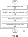
- a number of quantum dots are subjected to multiple rounds of silica coating or other insulator material, for example, by sol-gel process, combined with base treatment after each round of coating.
- Quantum dots are coated with a first insulating layer 715 at 205A. This first insulating layer may be added via a reverse micelle method, a direct micelle method, or some other sol-gel process.
- coated quantum dots are then treated at 210A with base (caustic), followed at 215A by removing excess or un-reacted base to ensure that a correct amount of base, which acts as a catalyst, is used for adding another insulating layer. Finally, one or more insulating layers 715 are added at 220A, with a base treatment after each round of coating.
- base caustic
- one or more insulating layers 715 are added at 220A, with a base treatment after each round of coating.
- a first layer of silica may be formed around individual quantum dots using a sol-gel process, such as a reverse micelle sol-gel reaction.
- a sol-gel process such as a reverse micelle sol-gel reaction.
- the silica coated quantum dots are treated with base or a mixture of different bases either by adding base(s) directly to a concentrated quantum dot stock solution in solvent or to a diluted solution of quantum dots.
- excess or un-reacted base is removed by one or more rounds of wash with an appropriate solvent, such as methanol and ethanol.
- More silica layers can then be grown on the basetreated silica coated quantum dots.
- the subsequent silica coating additions can be accomplished in several ways: (1) by a reverse micelle sol-gel process as described in U.S. patent application Ser. No. 13/485,756 ; (2) by a direct micelle sol-gel process as described in US patent application Ser. No. 13/972,700 , or (3) by a Stober sol-gel process.
- a plurality of quantum dots is subjected to multiple rounds of sol-gel processing combined with acid treatment, as opposed to base treatment, after each round of processing.
- a first layer of silica is formed around the quantum dots at 205B, using a sol-gel process, for example, using a reverse micelle sol-gel reaction.
- the silica shelled quantum dots are then treated with an acid or a mixture of different acids either by adding acid(s) directly to a concentrated quantum dot stock solution in solvent or to a diluted solution of quantum dots, at 210B.
- excess or un-reacted acid is removed at 215B with one or more rounds of wash with an appropriate solvent, such as methanol and ethanol, ensuring that a correct amount of catalyst base is used for the application of additional layers.
- an appropriate solvent such as methanol and ethanol
- the silica layer addition can be accomplished in several ways: (1) by a reverse micelle sol-gel process; (2) by a direct micelle sol-gel; (3) by a Stober sol-gel process, or (4) by a sol-gel process that acidifies the aqueous solution of metal silicate.
- a plurality of quantum dots is subjected to multiple rounds of insulator coating by sol-gel processes combined with no chemical treatment after each round of coating.
- a first layer of silica is formed around the quantum dots at 205C, for example, using a sol-gel process, such as a reverse micelle sol-gel reaction.
- the silica coated quantum dots are then purified at 207C.
- the silica coated quantum dots are subjected at 315C to another round or more of silica coating by any of the following ways: (1) by a reverse micelle sol-gel; (2) by a direct micelle sol-gel process; (3) by a Stober sol-gel process, or (4) by a sol-gel process that acidifies the aqueous solution of metal silicate.
- a layer of silica is formed at 205D around each of the quantum dots using a sol-gel process, such as a reverse micelle sol-gel reaction.
- the layer can then be treated with base, or acid, or may receive no treatment, at 310D. If the first insulating layer is treated with base or acid, the process continues at 315D with removal of any excess base or acid.
- the silica coated quantum dots are subjected to another one or more rounds of silica coating by any of the following ways: (1) by a reverse micelle sol-gel process; (2) by a direct micelle sol-gel process; (3) by a Stober sol-gel process, or (4) by a sol-gel process that acidifies the aqueous solution of metal silicate.
- the additional layers of silica coating can be treated again with base or acid or may receive no treatment and additional layers of silica coating can be added using any of the above methods.
- FIG. 2 is an image from a TEM of coated quantum dots resulting from using a syringe pump.
- multilayers consist of alternating organic and inorganic layers that encapsulate the metal-oxide coated quantum dots.
- multilayer encapsulation include alternating layers of inorganic materials such as Al 2 0 3 , MgO, and SiO x , and SiN x as well as transition metals including copper, cobalt, and iron deposited by ALD.
- Parylene is an exemplary organic layer in multilayer structures and may serve as the final layer due to its low modulus and hydrophobic nature. Also, a final layer of Parylene keeps water from condensing on the Al 2 0 3 layer, which is known to corrode Al 2 0 3 .
- Parylene may also help with stress relaxation during the addition of the multiple inorganic layers. Parylene can be introduced by vapor-phase deposition between or after the addition of the inorganic layers. The Parylene deposition can be done at room temperature, eliminating any risk of thermal damage to the samples.
- FIG. 3 provides TEM images 300 of quantum dot particles coated with metal oxide layers of varying thickness. Parylene is the trade name for a variety of chemical vapor deposited poly (p-xylylene) polymers.
- water-absorbing polymers can be used as organic layers to protect quantum dots from humid environments.
- Water absorbing polymers include but are not limited to poly(vinyl alcohol) PVA, poly(ethylene oxide) PEO, polyacrylamide, polyacrylate, poly(acrylic acid) and partially neutralised, lightly cross-linked poly(acrylic acid).
- a hydroxyl group (OH group) on the outer surface of a silica shell insulator layer surface can be first reacted with cyanuric chloride, a multifunctional crosslinker.
- PVA can be attached to the silica shell outer surface by reacting with cyanuric chloride.
- the silica shell is first modified with aminosilanes to provide amino functional groups on the outer surface.
- poly(acrylic acid) can be attached to the silica shell outer surface.
- the LBL assembly includes immersing a charged substrate, for instance, quantum dots negatively charged with poly(acrylic acid), in a solution of positively charged polyelectrolyte such as poly (diallyldimethylammonium) (PDDA). After rinsing with water, PDDA forms a positively charged monolayer on the surface of the substrate. Immersion in a solution of negatively charged polyelectrolyte forms a new layer, thereby switching the surface charge. This cycle can be repeated as many times as desired to assemble layers of water absorbing polymers on the quantum dots.
- a charged substrate for instance, quantum dots negatively charged with poly(acrylic acid)
- PDDA poly (diallyldimethylammonium)
- quantum dots comprising core 705 and shell 710, with multiple insulator coatings 715 for use in, as an example, on-chip light emitting diode applications.
- a number of quantum dots are subjected to multiple rounds of silica coating or other insulator material, for example, by sol-gel process, optionally combined with acid or base treatment after each round of coating.
- Quantum dots are coated with a first insulating layer 715 at 205A/205B/205C and 205D.
- this first insulating layer may be added via a reverse micelle method, a direct micelle method, or some other sol-gel process.
- the method combines quantum dots, surfactants, an aminosilane, and a silica precursor in order to grow the first silica shell insulating layer.
- the chemicals are similar as described in the above embodiments, but micelles are not being formed, so the embodiment does not involve a reverse micelle process.
- quantum dots are dispersed in cyclohexane (Cy) liquid at 205E to create a solution.
- a surfactant such as polyoxyethylene (5) nonylphenylether, is added to the solution at 210E.
- an aminosilane is added to the quantum dot solution at 215E.
- an alcohol (MeOH, EtOH, IPA. etc) is added at 220E.
- the role of the surfactant used here is to help disperse quantum dots having non-polar hydrophobic ligands on the surface in a polar solvent like alcohol.
- the quantum dot solution is optically clear.
- ammonium hydroxide and tetraorthosilicate (TEOS) are added to the quantum dot solution at 225E to start the reaction to coat the quantum dots with silica shell.
- this embodiment is more effective in growing large silica particles with diameters of hundreds of nanometers to a few microns. Unlike the micelle method, there is no size limiting micelle formed in this embodiment. Therefore the silica particles can grow much larger.
- quantum dots with non-polar organic ligands on the surface are exchanged with polar ligands such as polyallylamine and polyethylenimine in order to grow the first silica shell insulating layer.
- polar ligands such as polyallylamine and polyethylenimine
- These amine polymers have multiple binding groups to allow them to hold onto the quantum dots much tighter than the mono dentate ligands widely used in the quantum dot synthesis.
- the amine polymers are soluble in both alcohol and water, allowing the silica shell growth around the quantum dots by the Stober sol-gel process to grow large particles effectively.
- quantum dots with non-polar organic ligands on the surface are mixed with aminosilanes with stirring at 205F.
- Polyethylenimine dissolved in alcohol is then added to the quantum dots and stirred overnight at room or elevated temperature at 210F.
- polyallylamine is used instead of polyethylenimine.
- no aminosilane is added to the quantum dots at 205F.
- the quantum dots are mixed directly with polyallyamine or polyethylemine at 210F.
- excess solvents can be removed using a rotary evaporator at 215F.
- water or alcohol is added to disperse the quantum dots at 220F.
- the quantum dots are purified using an ultrafiltration filter to remove excess polymer at 225F.
- silica shell insulating layers can be grown around the polyamine coated quantum dots at 230F using Stober sol-gel method, by simply mixing quantum dots with tetraorthosilicate (TEOS) or any suitable precursor and ammonium hydroxide in alcohol/water mixture.
- TEOS tetraorthosilicate
- a semiconductor structure includes a nanocrystalline core composed of a first semiconductor material.
- the semiconductor structure also includes a nanocrystalline shell composed of a second, different, semiconductor material at least partially surrounding the nanocrystalline core.
- Additional nanocrystalline shells may also be formed that surround the core/shell pairing.
- An insulator layer encapsulates, e.g., coats, the nanocrystalline shell and nanocrystalline core.
- coated semiconductor structures include coated structures such as the quantum dots described above.
- the nanocrystalline core is anisotropic, e.g., having an aspect ratio between, but not including, 1.0 and 2.0.
- the nanocrystalline core is anisotropic and is asymmetrically oriented within the nanocrystalline shell.
- the nanocrystalline core and the nanocrystalline shell form a quantum dot.
- one or more additional semiconductor layers may be surround the quantum dot.
- An insulator layer may be formed so that it encapsulates, e.g., coats, the final semiconductor layer.
- the coated quantum dot may be coated with subsequent insulator layers. In between the formation of each insulator layer, the coated quantum dot may optionally be treated with an acid or base as described above.
- the insulator layer is bonded directly to the nanocrystalline shell.
- the insulator layer passivates an outermost surface of the nanocrystalline shell.
- the insulator layer provides a barrier for the nanocrystalline shell and nanocrystalline core impermeable to an environment outside of the insulator layer.
- the insulator layer may encapsulate only a single nanocrystalline shell/nanocrystalline core pairing.
- the semiconductor structure further includes a nanocrystalline outer shell at least partially surrounding the nanocrystalline shell, between the nanocrystalline shell and the insulator layer.
- the nanocrystalline outer shell is composed of a third semiconductor material different from the semiconductor material of the shell and, possibly, different from the semiconductor material of the core
- the insulator layer is composed of a layer of material such as, but not limited to, silica (SiOx), titanium oxide (TiOx), zirconium oxide (ZrOx), alumina (AlOx), or hafnia (HfOx).
- the layer is silica having a thickness approximately in the range of 3-500 nanometers.
- the insulator layer is an amorphous layer.
- an outer surface of the insulator layer is ligand-free.
- an outer surface of the insulator layer is ligand-functionalized.
- the outer surface of the insulator layer is ligand-functionalized with a ligand such as, but not limited to, a silane having one or more hydrolyzable groups or a functional or non-functional bipodal silane.
- the outer surface of the insulator layer is ligand functionalized with a ligand such as, but not limited to, mono-, di-, or tri-alkoxysilanes with three, two or one inert or organofunctional substituents of the general formula (R10)3SiR2; (R10)2SiR2R3; (RIO) SiR2R3R4, where R1 is methyl, ethyl, propyl, isopropyl, or butyl, R2, R3 and R4 are identical or different and are H substituents, alkyls, alkenes, alkynes, aryls, halogeno-derivates, alcohols, (mono, di, tri, poly) ethyleneglycols, (secondary, tertiary, quaternary) amines, diamines, polyamines, azides, isocyanates, acrylates, metacrylates, epoxies, ethers, aldehydes,
- the outer surface of the insulator layer is ligand-functionalized with a ligand such as, but not limited to, organic or inorganic compounds with functionality for bonding to a silica surface by chemical or non-chemical interactions such as but not limited to covalent, ionic, H-bonding, or Van der Waals forces.
- a ligand such as, but not limited to, organic or inorganic compounds with functionality for bonding to a silica surface by chemical or non-chemical interactions such as but not limited to covalent, ionic, H-bonding, or Van der Waals forces.
- the outer surface of the insulator layer is ligand-functionalized with a ligand such as, but not limited to, the methoxy and ethoxy silanes (MeO)3SiAllyl, (MeO)3SiVinyl, (MeO)2SiMeVinyl, (EtO)3SiVinyl, EtOSi(Vinyl)3, mono-methoxy silanes, chloro-silanes, or 1,2-bis-(triethoxysilyl)ethane.
- a ligand such as, but not limited to, the methoxy and ethoxy silanes (MeO)3SiAllyl, (MeO)3SiVinyl, (MeO)2SiMeVinyl, (EtO)3SiVinyl, EtOSi(Vinyl)3, mono-methoxy silanes, chloro-silanes, or 1,2-bis-(tri
- the outer surface of the insulator layer is ligand-functionalized to impart solubility, dispersability, heat stability, photo-stability, or a combination thereof, to the semiconductor structure.
- the outer surface of the insulator layer includes OH groups suitable for reaction with an intermediate linker to link small molecules, oligomers, polymers or macromolecules to the outer surface of the insulator layer, the intermediate linker one such as, but not limited to, an epoxide, a carbonyldiimidazole, a cyanuric chloride, or an isocyanate.
- the nanocrystalline core has a diameter approximately in the range of 2-6 nanometers.
- the nanocrystalline shell has a long axis and a short axis, the long axis having a length approximately in the range of 6-40 nanometers, and the short axis having a length approximately in the range of 1 -10 nanometers greater than the diameter of the nanocrystalline core.
- the insulator layer has a thickness approximately in the range of 1 -50 nanometers along an axis co-axial with the long axis and has a thickness approximately in the range of 3-50 nanometers along an axis co-axial with the short axis. In other embodiments, the thickness of the insulator layer may be greater than 50 nanometers, for example, up to 500 nanometers.
- a lighting apparatus may include a light emitting diode and a plurality of semiconductor structures that, for example, act to down convert light absorbed from the light emitting diode.
- each semiconductor structure includes a quantum dot having a nanocrystalline core composed of a first semiconductor material and a nanocrystalline shell composed of a second different, semiconductor material at least partially surrounding the nanocrystalline core.
- Each quantum dot has a photoluminescence quantum yield (PLQY) of at least 90%.
- PLQY photoluminescence quantum yield
- Each quantum dot may optionally have additional semiconductor layers.
- an insulator layer may be formed to encapsulate a nanocrystalline shell and anisotropic nanocrystalline core.
- a layer of silica is formed using a reverse micelle sol-gel reaction.
- using the reverse micelle sol-gel reaction includes dissolving the nanocrystalline shell/nanocrystalline core pairing in a first non-polar solvent to form a first solution.
- the first solution is added along with a species such as, but not limited to, 3-aminopropyltrimethoxysilane (APTMS), 3-mercaptotrimethoxysilane, or a silane comprising a phosphonic acid or carboxylic acid functional group, to a second solution having a surfactant dissolved in a second non-polar solvent.
- a species such as, but not limited to, 3-aminopropyltrimethoxysilane (APTMS), 3-mercaptotrimethoxysilane, or a silane comprising a phosphonic acid or carboxylic acid functional group
- ATMS 3-aminopropyltrimethoxysilane
- TEOS tetraorthosilicate
- FIG. 4 illustrates operations in a reverse micelle approach to coating a semiconductor structure, in accordance with an embodiment of the present invention.
- a quantum dot heterostructure (QDH) 502 e.g., a nanocrystalline core/shell pairing
- TOPO trioctylphosphine oxide
- TOP trioctylphosphine
- the plurality of TOPO ligands 404, TOP ligands 406, and Oleic Acid 405, are exchanged with a plurality of Si(OCH3)3(CH2)3NH2 ligands 408.
- the structure of part B is then reacted with TEOS (Si(OEt)4) and ammonium hydroxide (NH40H) to form a silica coating 410 surrounding the QDH 402, as depicted in part C of FIG. 4 .
- the first and second non-polar solvents are cyclohexane.
- forming the coating layer includes forming a layer of silica and further includes using a combination of dioctyl sodium sulfosuccinate (AOT) and tetraorthosilicate (TEOS).
- AOT dioctyl sodium sulfosuccinate
- TEOS tetraorthosilicate
- forming the layer includes forming a layer of silica and further includes using a combination of polyoxyethylene (5) nonylphenylether and tetraorthosilicate (TEOS).
- forming the layer includes forming a layer of silica and further includes using cationic surfactants such as CTAS (cetyltrimethylannnonium bromide), anionic surfactants, non-ionic surfactants, or pluronic surfactants such as Pluronic F 127 (an ethylene oxide/propylene oxide block co-polymer) as well as mixtures of surfactants.
- CTAS cetyltrimethylannnonium bromide
- anionic surfactants such as anionic surfactants, non-ionic surfactants, or pluronic surfactants such as Pluronic F 127 (an ethylene oxide/propylene oxide block co-polymer) as well as mixtures of surfactants.
- Pluronic F 127 an ethylene oxide/propylene oxide block co-polymer
- silica coatings may be conformal to the core/shell QDH or non-conformal.
- a silica coating may be between about 3 nm and 500 nm thick.
- the silica coating thickness along the c-axis may be as small as about 1 nm or as large as about 500 nm.
- the silica coating thickness along the a-axis may be between about 3 nm and 500 nm.
- silicacoated quantum dots can then be incorporated into a polymer matrix or undergo further surface functionalization.
- silica layers according to embodiments of the present invention may also be functionalized with ligands to impart solubility, dispersability, heat stability and photostability in the matrix.
- quantum dot composite compositions are described.
- the quantum dots (including coated quantum dots) described above may be embedded in a matrix material to make a composite using a plastic or other material as the matrix.
- composite compositions including matrix materials and silica coated core/shell quantum dots having photoluminescence quantum yields between 90 and 100% are formed.
- Such quantum dots may be incorporated into a matrix material suitable for down converting in LED applications.
- a semiconductor structure has a nanocrystalline core and nanocrystalline shell pairing with one compositional transition layer, in accordance with an embodiment of the present invention.
- a semiconductor structure 500 includes a nanocrystalline core 502 composed of a first semiconductor material.
- a nanocrystalline shell 504 composed of a second, different, semiconductor material at least partially surrounds the nanocrystalline core 502.
- a compositional transition layer 510 is disposed between, and in contact with, the nanocrystalline core 502 and nanocrystalline shell 504.
- the compositional transition layer 510 has a composition intermediate to the first and second semiconductor materials.
- the compositional transition layer 510 is an alloyed layer composed of a mixture of the first and second semiconductor materials. In another embodiment, the compositional transition layer 510 is a graded layer composed of a compositional gradient of the first semiconductor material proximate to the nanocrystalline core 502 through to the second semiconductor material proximate to the nanocrystalline shell 504. In either case, in a specific embodiment, the compositional transition layer 510 has a thickness approximately in the range of 1.5-2 monolayers.
- Exemplary embodiments include a structure 500 where the first semiconductor material is cadmium selenide (CdSe), the second semiconductor material is cadmium sulfide (CdS), and the compositional transition layer 510 is composed of CdSexSy, where 0 ⁇ x ⁇ l and 0 ⁇ y ⁇ l, or where the first semiconductor material is cadmium selenide (CdSe), the second semiconductor material is zinc selenide (ZnSe), and the compositional transition layer 510 is composed of CdxZnySe, where 0 ⁇ x ⁇ l and 0 ⁇ y ⁇ l.
- CdSe cadmium selenide
- CdSe cadmium sulfide
- the compositional transition layer 510 is composed of CdSexSy, where 0 ⁇ x ⁇ l and 0 ⁇ y ⁇ l, or where the first semiconductor material is cadmium selenide (CdSe), the second semiconductor material is zinc selenide (ZnSe), and the compositional transition layer
- the nanocrystalline shell 504 completely surrounds the nanocrystalline core 502, as depicted in FIG. 5 . In an alternative embodiment, however, the nanocrystalline shell 504 only partially surrounds the nanocrystalline core 502, exposing a portion of the nanocrystalline core 502. Furthermore, in either case, the nanocrystalline core 502 may be disposed in an asymmetric orientation with respect to the nanocrystalline shell 504. In one or more embodiments, semiconductor structures such as 500 are fabricated to further include a nanocrystalline outer shell 506 at least partially surrounding the nanocrystalline shell 504. The nanocrystalline outer shell 506 may be composed of a third semiconductor material different from the first and second semiconductor materials, i.e., different from the materials of the core 502 and shell 504.
- the nanocrystalline outer shell 506 may completely surround the nanocrystalline shell 504 or may only partially surround the nanocrystalline shell 504, exposing a portion of the nanocrystalline shell 504.
- an insulator layer 508 encapsulates the shell 506. In one embodiment, multiple insulator layers may be applied, as described elsewhere herein.
- a network of quantum dots may be formed by fusing together the insulator coatings of a plurality of insulator coated quantum dots.
- insulator coatings of discrete passivated quantum dots are fused together to form a substantially rigid network of quantum dots where each quantum dot is isolated from other quantum dots in the network by the fused insulator coating.
- fusing together the insulator coatings of discretely passivated quantum dots into a fused network provides improved optical and reliability performance of the resulting structure as compared with the starting discretely passivated quantum dots.
- a chemical base is used to improve the optical performance of silica coated materials by enabling the fusing of the insulator coatings surrounding a plurality of quantum dots.
- the insulator coatings is a silica coating and a base such as potassium hydroxide (KOH) is used to fuse together the silica coatings of a plurality of individually and discretely coated quantum dots.
- KOH potassium hydroxide
- the result is a substantially rigid silica-based network of quantum dots.
- the amount of base material is scaled with the amount of silica in the reaction.
- the approaches described herein have important applications for improving the optical and reliability performance of quantum dots or even other phosphor materials having an insulator coating and which are embedded in a matrix.
- the quantum dots or other phosphor materials are first individually coated with one or more insulator layers and then the coated materials are fused to form an insulator network that can be embedded in a matrix.
- the insulator network is formed directly on the quantum dots or other phosphor materials.
- quantum dots are individually coated with a silica insulator layer.
- the presence of the silica coating improves the performance of the quantum dots when they are subsequently embedded in a polymer film and subjected to various stress tests.
- Applications include LED lighting applications and/or display configurations.
- base such as KOH, NaOH or other similar materials
- the scaling of the amount of KOH or other base with silica content is balanced to achieve optimal performance of the coated/fused quantum dots.
- a method of fabricating a semiconductor structure involves forming a mixture including a plurality of discrete semiconductor quantum dots. Each of the plurality of discrete semiconductor quantum dots is discretely coated by an insulator layer. The method also involves adding a base to the mixture to fuse the insulator layers of each of the plurality of discrete quantum dots, providing an insulator network. Each of the plurality of discrete semiconductor quantum dots is spaced apart from one another by the insulator network.
- the base may be comprised of, but not limited to, LiOH, RbOH, CsOH, MgOH, Ca(OH)2, Sr(OH)2, Sa(OH)2, (Me)4NOH, (Et)4NOH, or (Bu)4NOH.
- a method of fabricating a semiconductor structure involves forming a mixture including a plurality of discrete semiconductor quantum dots. Each of the plurality of discrete semiconductor quantum dots is discretely coated by an insulator material. The method also involves adding a base to the mixture to fuse the insulator coating of each of the plurality of discrete quantum dots, providing an insulator network. Each of the plurality of discrete semiconductor quantum dots is spaced apart from one another by the insulator network.
- the base may be comprised of, but not limited to, LiOH, RbOH, CsOH, MgOH, (Me)4NOH, (Et)4NOH, or (Su)4NOH, and adding the base to the mixture involves adding one mole of the base for every two moles of the insulator material.
- the method also involves adding free silica to the mixture.
- a method of fabricating a semiconductor structure involves forming a mixture including a plurality of discrete semiconductor quantum dots. Each of the plurality of discrete semiconductor quantum dots is discretely coated by an insulator material. The method also involves adding a base to the mixture to fuse the insulator coating of each of the plurality of discrete quantum dots, providing an insulator network. Each of the plurality of discrete semiconductor quantum dots is spaced apart from one another by the insulator network.
- the base may be comprised of, but not limited to, Ca(OH)2, Sr(OH)2 or Sa(OH)2, and adding the base to the mixture involves adding one mole of the base for every four moles of the insulator material.
- the method also involves adding free silica to the mixture.
- an alternative to altering seed size for tuning the emission of a seeded rod emitter architecture is provided. More particularly, instead of changing seed size, the seed composition is changed by alloying either the entire seed (in one embodiment) or some portion of the seed (in another embodiment) with a higher bandgap material. In either case, the general approach can be referred to as an alloying of the seed or nanocrystalline core portion of a heterostructure quantum dot. By alloying the seed or nanocrystalline core, the bandgap can be changed without changing the size of the seed or core. As such, the emission of the seed or core can be changed without changing the size of the seed or core.
- the size of the seed is fixed at the optimum size of a red-emitting seed, or roughly 4 nanometers.
- the fixed sized means that the size of the rod and the subsequent synthetic operations may not need to be substantially re-optimized or altered as the emission target of the quantum dots is changed.
- a quantum dot includes an alloyed Group II-VI nanocrystalline core.
- the quantum dot also includes a Group II-VI nanocrystalline shell composed of a semiconductor material composition different from the alloyed Group II-VI nanocrystalline core.
- the Group II-VI nanocrystalline shell is bonded to and completely surrounds the alloyed Group II-VI nanocrystalline core.
- the alloyed Group II-VI nanocrystalline core is composed of CdSenSl-n (0 ⁇ n ⁇ l), and the Group II-VI nanocrystalline shell is composed of CdS.
- the alloyed Group II-VI nanocrystalline core has a shortest diameter of greater than approximately 2 nanometers, and the quantum dot has an exciton peak less than 555 nanometers.
- the alloyed Group II-VI nanocrystalline core has a shortest diameter of approximately 4 nanometers, and the quantum dot has an exciton peak less than 555 nanometers, as is described in greater detail below.
- a quantum dot includes a semiconductor nanocrystalline core of arbitrary composition.
- the quantum dot also includes any number of semiconductor nanocrystalline shell(s).
- the semiconductor nanocrystalline shell(s) is/are bonded to and completely surrounds the semiconductor nanocrystalline core.
- the semiconductor nanocrystalline core is composed of a first Group II-VI material
- the binary semiconductor nanocrystalline shell is composed of a second, different, Group II-VI material.
- the first Group II-VI material is CdSenSl-n (0 ⁇ n ⁇ l)
- the second Group II-VI material is CdS.
- the semiconductor hetero-structure has a nano-crystalline core composed of a group semiconductor material.
- a nanocrystalline shell composed of a second, different, semiconductor material at least partially surrounds the nano-crystalline core.
- the nano-crystalline shell may be composed of a different group I-III-VI semiconductor material or of a group II-VI semiconductor material.
- the above described nano-crystalline core/nano-crystalline shell pairing has a photoluminescence quantum yield (PLQY) of greater than approximately 60%.
- the nano-crystalline core/nano-crystalline shell pairing provides a Type I hetero-structure.
- One or more embodiments described herein are directed to hetero-structure systems having distinct group I-III-VI material cores.
- a sphere or rod-shaped core/shell quantum dot is fabricated to have a sharp compositional interface between the core and shell or a graded/alloyed interface between core and shell.
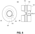
- FIG. 6 illustrates an axial cross-sectional view (A) of a spherical nano-particle 600, in accordance with an embodiment of the present invention.
- an alloy region 606 is included between the core 602 and shell 604 of 600.
- the nano-particle 600 demonstrates type I heterostructure behavior, with excitons preferentially recombining in the core 602 of the nano-crystal 600 due to the smaller, nested bandgap of the seed.
- additional layers of material may be added, including additional epitaxial layers or amorphous inorganic and organic layers. Other suitable embodiments are described below.
- systems described herein include a nano-crystalline core emitter having a direct, bulk band gap approximately in the range of 1 -2.5 eV.
- exemplary cores include a group I-III-VI semiconductor material based on silver gallium sulfide having a stoichiometry of approximately AgGaS2.
- the nanocrystalline core has a peak emission approximately in the range of 475-575 nanometers.
- the nano-crystalline core and nano-crystalline shell pairings described herein have a lattice mismatch of equal to or less than approximately 10%. In some embodiments, less than approximately 6% mismatch is preferable, but up to approximately 10% can be workable. In particular embodiments, the mismatch is less than approximately 4% mismatch, as seen in successful Cd-based systems.
- the first (core) material is a group I-III-VI semiconductor material.
- the second (shell) semiconductor material is a second group I-III-VI material.
- a suitable I-III-VI/I-III-VI core/shell pairing can include, but is not limited to, copper indium sulfide (CIS)/silver gallium sulfide (AgGaS2), copper indium selenide (CISe)/AgGaS2, copper gallium selenide (CuGaSe2)/copper gallium sulfide (CuGaS2), or CuGaSe2/AgGaS2.
- the second (shell) semiconductor material is a group II-VI material.
- a suitable I-III-VI/II-VI core/shell pairing can include, but is not limited to, copper indium sulfide (CIS)/zinc selenide (ZnSe), CIS/zinc sulfide (ZnS), copper indium selenide (CISe)/ZnSe, CISe/ZnS, copper gallium selenide (CuGaSe2)/ZnSe, CuGaSe2/ZnS, silver gallium sulfide (AgGaS2)/ZnS, AgGaS2/ZnSe, or silver gallium selenide (AgGaSe2)/ZnS, AgGaSe2/ZnSe.
- the semiconductor hetero-structure further includes a nano-crystalline outer shell composed of a third semiconductor material different from the core and shell semiconductor materials.
- the third semiconductor material at least partially surrounding the nano-crystalline shell and, in one embodiment, the nano-crystalline outer shell completely surrounds the nano-crystalline shell.
- the second (shell) semiconductor material one such as, but not limited to, zinc selenide (ZnSe), silver gallium sulfide (AgGaS2) or copper gallium sulfide (CuGaS2)
- the third (outer shell) semiconductor material is zinc sulfide (ZnS).
- the shape of the core of the quantum dot depicted in FIG. 4 is a that of a rod
- the methods described herein are not limited by the shape of the quantum dot and could be applied to coated quantum dots of many different shapes, including but not limited to spheres, rods, tetrapods, teardrops, sheets, etc. It is not limited by the composition of the quantum dot and can be applied to quantum dots made from a single material or multiple materials in either a core/shell/optional shell/optional shell configuration or an alloyed composition.
- the semiconductor materials may be selected from the Group II-VI compounds, Group III-V compounds, group IV-IV compounds, group I-III-VI compounds, or any alloy thereof.
- the semiconductor materials may be chosen from ZnO, ZnS, ZnSe, ZnTe, CdO, CdS, CdSe, CdTe, HgS. HgSe, HgTe, HgO, AIN, ATP, AlAs, AlSb, GaN, GaP, GaAs, GaSb, GaSe, InN, InP, InAs, InSb, TIN, TIP, TIAs, TISb, PbS, PbSe, PbTe, MgO, MgS, MgSe, alloys thereof, and mixtures thereof.
Landscapes
- Chemical & Material Sciences (AREA)
- Engineering & Computer Science (AREA)
- Materials Engineering (AREA)
- Organic Chemistry (AREA)
- Luminescent Compositions (AREA)
Claims (15)
- Ein Verfahren zur Herstellung einer Halbleiterstruktur, dadurch gekennzeichnet, dass das Verfahren aufweist:Bilden eines nanokristallinen Kerns aus einem ersten Halbleitermaterial;Bilden zumindest einer nanokristallinen Hülle aus einem zweiten, anderen, Halbleitermaterial, das zumindest teilweise den nanokristallinen Kern umgibt,Bilden einer nanokristallinen äußeren Hülle aus einem dritten Halbleitermaterial, das anders als das Halbleitermaterial der nanokristallinen Schale ist, die die nanokristalline Hülle zumindest teilweise umgibt, wobei der nanokristalline Kern und die nanokristalline(n) Hülle(n) einen Quantenpunkt bilden;Bilden einer Isolatorschicht aufweisend eine erste Metalloxidschicht, die den Quantenpunkt und die äußere Hülle verkapselt, um einen beschichteten Quantenpunkt zu erzeugen; undBilden zumindest einer zusätzlichen Isolatorschicht auf dem beschichteten Quantenpunkt, aufweisend Bilden zumindest einer organischen Schicht aus wasserabsorbierenden Polymer, wobei das wasserabsorbierende Polymer ausgewählt ist aus einer Gruppe bestehend aus: Poly(ethylenoxid) PEO, Polyacrylamid, Polyacrylat und Poly(acrylsäure).
- Das Verfahren nach einem der vorhergehenden Ansprüche, wobei Bilden der Isolatorschicht, die den Quantenpunkt verkapselt, um einen beschichteten Quantenpunkt zu erzeugen, Bilden einer ersten Isolatorschicht, die den Quantenpunkt verkapselt, unter Verwendung eines Sol-Gel-Verfahrens aufweist; und wobei
Bilden der zusätzlichen Isolatorschichten auf dem beschichteten Quantenpunkt Bilden einer zusätzlichen isolierenden Schicht, die den Quantenpunkt verkapselt, unter Verwendung eines Sol-Gel-Verfahrens aufweist. - Das Verfahren nach Anspruch 2, wobei
Bilden einer ersten Isolatorschicht, die den Quantenpunkt verkapselt, unter Verwendung eines Sol-Gel-Verfahrens Bilden der ersten Isolatorschicht, die den Quantenpunkt verkapselt, unter Verwendung eines Umkehrmizellen-Sol-Gel-Verfahrens aufweist; und wobei Bilden der zusätzlichen isolierenden Schicht, die den Quantenpunkt verkapselt, unter Verwendung eines Sol-Gel-Verfahrens Bilden der zusätzlichen isolierenden Schicht, die den Quantenpunkt verkapselt, unter Verwendung eines der folgenden Verfahren aufweist: Umkehrmizellen-Sol-Gel-Verfahren, ein direktes Mizellen-Sol-Gel-Verfahren, ein Stober-Sol-Gel-Verfahren und ein Sol-Gel-Verfahren, das den verkapselten Quantenpunkt ansäuert. - Das Verfahren nach einem der vorhergehenden Ansprüche, wobei
Bilden der Isolatorschicht, die den Quantenpunkt verkapselt, um einen beschichteten Quantenpunkt zu erzeugen, Bilden einer ersten Isolatorschicht, die den Quantenpunkt verkapselt, durch:Dispergieren des Quantenpunkts in Lösung;Zugabe eines Netzmittels zu der Lösung;Zugabe von Aminosilan zu der Lösung;Zugabe von Alkohol zu der Lösung; undZugabe von Ammoniumhydroxid und Tetraorthosilikat zu der Lösung, aufweist. - Das Verfahren nach einem der vorhergehenden Ansprüche, wobei
Bilden der Isolatorschicht, die den Quantenpunkt verkapselt, um einen beschichteten Quantenpunkt zu erzeugen, Bilden einer ersten Isolatorschicht, die den Quantenpunkt verkapselt, durch:Mischen unpolarer Liganden auf der Oberfläche des Quantenpunkts mit Aminosilanen;Zugabe von in Alkohol gelöstem Polyethylenimin zu dem Quantenpunkt;Dispergieren des Quantenpunkts in Wasser oder Alkohol; undZugabe von Ammoniumhydroxid und Tetraorthosilikat, aufweist. - Das Verfahren nach einem der vorhergehenden Ansprüche, wobei
nach Bilden der Isolatorschicht, die den Quantenpunkt verkapselt, um einen beschichteten Quantenpunkt zu erzeugen, und vor Bilden der zumindest einen zusätzlichen Isolatorschicht auf dem beschichteten Quantenpunkt, Behandeln des beschichteten Quantenpunkts mit einer Base oder einer Säure. - Das Verfahren nach einem der vorhergehenden Ansprüche, wobei
nach Bilden der zumindest einen zusätzlichen Isolatorschicht auf dem beschichteten Quantenpunkt und vor weiterem Bilden zusätzlicher Isolatorschichten, die den Quantenpunkt verkapseln, Behandeln des beschichteten Quantenpunkts mit einer Base oder einer Säure. - Das Verfahren nach einem der vorhergehenden Ansprüche, wobei
Bilden der Isolatorschicht, die den Quantenpunkt einkapselt, um einen beschichteten Quantenpunkt zu erzeugen, oder Bilden der zumindest einen zusätzlichen Isolatorschicht auf dem beschichteten Quantenpunkt während des Siliziumdioxid-Beschichtungsprozesses einen der folgenden Schritte aufweist:zumindest einmaliges Einspritzen eines Silikagel-bildenden Vorläufers während dem Bilden, mehrmaliges Einspritzen des Silikagel-bildenden Vorläufers während dem Bilden, undEinspritzen des Silikagel-bildenden Vorläufers unter Verwendung einer Spritzenpumpe mit der gewünschten Geschwindigkeit. - Das Verfahren nach einem der vorhergehenden Ansprüche, ferner aufweisend
Ligandenfunktionalisieren einer äußere Oberfläche der Isolatorschicht mit einem Liganden ausgewählt aus einer Gruppe bestehend aus organischen Verbindungen und anorganischen Verbindungen, mit Ligandenfunktionalität zur Bindung an die äußere Oberfläche durch chemische oder nichtchemische Wechselwirkungen, die aus einer Gruppe ausgewählt sind, die besteht aus: kovalent, ionisch, H-Bindung und Vander-Waals-Kräfte. - Das Verfahren nach einem der vorhergehenden Ansprüche, ferner aufweisend
Ligandenfunktionalisieren einer äußeren Oberfläche der Isolatorschicht mit einem Liganden ausgewählt aus einer Gruppe bestehend aus: Methoxy- und Ethoxysilanen (MeO)3SiAllyl, (MeO)3SiVinyl, (MeO)2SiMeVinyl, (EtO)3SiVinyl, EtOSi(Vinyl)3, Monomethoxysilanen, Chlorsilanen und 1,2-Bis-(triethoxysilyl)ethan. - Eine Halbleiterstruktur, dadurch gekennzeichnet, dass die Halbleiterstruktur aufweist:einen nanokristallinen Kern aufweisend ein erstes Halbleitermaterial;zumindest eine nanokristalline Hülle aufweisend ein zweites, anderes, Halbleitermaterial, das zumindest teilweise den nanokristallinen Kern umgibt,eine nanokristalline äußere Hülle aus einem dritten Halbleitermaterial, das anders als das Halbleitermaterial der nanokristallinen Hülle ist, die die nanokristalline Hülle zumindest teilweise umgibt, wobei der nanokristalline Kern und die nanokristalline(n) Hülle(n) einen Quantenpunkt bilden;eine Isolatorschicht aufweisend eine erste Metalloxidschicht, die den Quantenpunkt und die äußere Hülle verkapselt, um einen beschichteten Quantenpunkt zu bilden; undzumindest eine zusätzliche Isolatorschicht, die den beschichtete Quantenpunkte verkapselt, die organische Schichten aufweist, wobeidie organischen Schichten zumindest eine Schicht eines wasserabsorbierenden Polymers aufweisen, das aus einer Gruppe ausgewählt ist, die aus Poly(ethylenoxid) PEO, Polyacrylamid, Polyacrylat und Poly(acrylsäure) besteht.
- Die Halbleiterstruktur nach Anspruch 11, wobei die Metalloxidschicht, die den Quantenpunkt verkapselt, aus einer Gruppe von Metalloxiden ausgewählt ist, die aus Siliziumdioxid (SiOx), Titanoxid (TiOx), Zirkoniumoxid (ZrOx), Aluminiumoxid (AlOx), Magnesiumoxid (MgOx) und Hafniumoxid (HfOx) besteht.
- Die Halbleiterstruktur nach einem der vorhergehenden Ansprüche 11 bis 12, wobei
die zusätzlichen Isolatorschichten auf dem beschichteten Quantenpunkt anorganischen Schichten auf dem beschichteten Quantenpunkt aufweisen. - Die Halbleiterstruktur nach einem der vorhergehenden Ansprüche 11 bis 13, wobei
die anorganischen Schichten eine Schicht mit einer Verbindung oder einem Metall ausgewählt aus einer Gruppe von Verbindungen und Metallen aufweisen, die aus Siliziumdioxid (SiOx), Titanoxid (TiOx), Zirkoniumoxid (ZrOx), Aluminiumoxid (AlOx), Magnesiumoxid (MgOx) und Hafniumoxid (HfOx) und SiNx Kupfer, Kobalt und Eisen besteht. - Eine Beleuchtungsvorrichtung, dadurch gekennzeichnet, dass die Beleuchtungsvorrichtung aufweist:eine Leuchtdiode; undeine Vielzahl von Quantenpunkten, jeder Quantenpunkt aufweisend einen nanokristallinen Kern aufweisend ein erstes Halbleitermaterial;zumindest eine nanokristalline Hülle aufweisend ein zweites, anderes, Halbleitermaterial, das zumindest teilweise den nanokristallinen Kern umgibt,eine nanokristalline äußere Hülle aus einem dritten Halbleitermaterial, das anders als das Halbleitermaterial der nanokristallinen Hülle ist, die die nanokristalline Hülle zumindest teilweise umgibt, wobei der nanokristalline Kern und die nanokristalline(n) Hülle(n) einen Quantenpunkt bilden;eine Isolatorschicht aufweisend eine erste Metalloxidschicht, die den Quantenpunkt und die äußere Hülle verkapselt, um einen beschichteten Quantenpunkt zu bilden; undzumindest eine zusätzliche Isolatorschicht, die den beschichteten Quantenpunkt verkapselt, die organische Schichten aufweist, wobei die organischen Schichten zumindest eine Schicht eines wasserabsorbierenden Polymers aufweisen, das aus einer Gruppe ausgewählt ist, die aus Poly(ethylenoxid) PEO, Polyacrylamid, Polyacrylat und Poly(acrylsäure) besteht.
Applications Claiming Priority (1)
| Application Number | Priority Date | Filing Date | Title |
|---|---|---|---|
| US15/391,685 US10266760B2 (en) | 2015-05-13 | 2016-12-27 | Composition of, and method for forming, a semiconductor structure with multiple insulator coatings |
Publications (2)
| Publication Number | Publication Date |
|---|---|
| EP3342841A1 EP3342841A1 (de) | 2018-07-04 |
| EP3342841B1 true EP3342841B1 (de) | 2023-03-01 |
Family
ID=60935662
Family Applications (1)
| Application Number | Title | Priority Date | Filing Date |
|---|---|---|---|
| EP17208584.7A Active EP3342841B1 (de) | 2016-12-27 | 2017-12-19 | Zusammensetzung von und verfahren zur formung einer halbleiterstruktur mit mehreren isolatorbeschichtungen |
Country Status (2)
| Country | Link |
|---|---|
| EP (1) | EP3342841B1 (de) |
| CN (1) | CN108269905B (de) |
Families Citing this family (3)
| Publication number | Priority date | Publication date | Assignee | Title |
|---|---|---|---|---|
| US10985336B1 (en) | 2020-01-06 | 2021-04-20 | Sharp Kabushiki Kaisha | Oxygen scavenging nanoparticles for air-processed quantum dot light emitting diodes |
| WO2022138905A1 (ja) * | 2020-12-25 | 2022-06-30 | Nsマテリアルズ株式会社 | 量子ドットの製造方法、及び、量子ドット |
| CN115627166B (zh) * | 2022-09-28 | 2024-04-12 | 江苏穿越光电科技有限公司 | 一种量子点及其制备方法和电致发光器件 |
Citations (1)
| Publication number | Priority date | Publication date | Assignee | Title |
|---|---|---|---|---|
| WO2016046216A1 (en) * | 2014-09-23 | 2016-03-31 | Philips Lighting Holding B.V. | Encapsulated materials in porous particles |
Family Cites Families (5)
| Publication number | Priority date | Publication date | Assignee | Title |
|---|---|---|---|---|
| GB0916699D0 (en) * | 2009-09-23 | 2009-11-04 | Nanoco Technologies Ltd | Semiconductor nanoparticle-based materials |
| WO2014208456A1 (ja) * | 2013-06-25 | 2014-12-31 | コニカミノルタ株式会社 | 光学材料、光学フィルム及び発光デバイス |
| US9249354B2 (en) * | 2013-07-03 | 2016-02-02 | Pacific Light Technologies Corp. | Network of semiconductor structures with fused insulator coating |
| US9831397B2 (en) * | 2015-03-09 | 2017-11-28 | Pacific Light Technologies Corp. | Quantum dots with multiple insulator coatings |
| DE112016003002T5 (de) * | 2015-06-30 | 2018-03-15 | Cree, Inc. | Stabilisierte Quantenpunktstruktur und Verfahren zur Herstellung einer stabilisierten Quantenpunktstruktur |
-
2017
- 2017-12-19 EP EP17208584.7A patent/EP3342841B1/de active Active
- 2017-12-26 CN CN201711430645.9A patent/CN108269905B/zh active Active
Patent Citations (1)
| Publication number | Priority date | Publication date | Assignee | Title |
|---|---|---|---|---|
| WO2016046216A1 (en) * | 2014-09-23 | 2016-03-31 | Philips Lighting Holding B.V. | Encapsulated materials in porous particles |
Also Published As
| Publication number | Publication date |
|---|---|
| EP3342841A1 (de) | 2018-07-04 |
| CN108269905B (zh) | 2020-04-21 |
| CN108269905A (zh) | 2018-07-10 |
Similar Documents
| Publication | Publication Date | Title |
|---|---|---|
| US10266760B2 (en) | Composition of, and method for forming, a semiconductor structure with multiple insulator coatings | |
| US10407613B2 (en) | Composition of, and method for forming, a semiconductor structure with polymer and insulator coatings | |
| EP3294834B1 (de) | Zusammensetzung von und verfahren zur formung einer halbleiterstruktur mit mehreren isolatorbeschichtungen | |
| EP3268981B1 (de) | Quantenpunkte mit mehreren isolatorbeschichtungen | |
| EP3297770B1 (de) | Isolatorbeschichtete quantenpunkte zur verwendung in der led-beleuchtung und anzeigevorrichtungen | |
| KR102686908B1 (ko) | 양자점들의 융합된 캡슐화 | |
| US20160336490A1 (en) | Methods for preparing quantum dots with insulator coatings | |
| CN108475694A (zh) | 低镉纳米晶体量子点异质结构 | |
| EP3493922B1 (de) | Beschichtete wellenlängenumwandlungsnanopartikel und verfahren zu deren herstellung | |
| EP3342841B1 (de) | Zusammensetzung von und verfahren zur formung einer halbleiterstruktur mit mehreren isolatorbeschichtungen | |
| US20170229619A1 (en) | Method and apparatus of applying light and heat to quantum dots to increase quantum yield | |
| US20180040783A1 (en) | Coated wavelength converting nanoparticles |
Legal Events
| Date | Code | Title | Description |
|---|---|---|---|
| PUAI | Public reference made under article 153(3) epc to a published international application that has entered the european phase |
Free format text: ORIGINAL CODE: 0009012 |
|
| STAA | Information on the status of an ep patent application or granted ep patent |
Free format text: STATUS: THE APPLICATION HAS BEEN PUBLISHED |
|
| AK | Designated contracting states |
Kind code of ref document: A1 Designated state(s): AL AT BE BG CH CY CZ DE DK EE ES FI FR GB GR HR HU IE IS IT LI LT LU LV MC MK MT NL NO PL PT RO RS SE SI SK SM TR |
|
| AX | Request for extension of the european patent |
Extension state: BA ME |
|
| RAP1 | Party data changed (applicant data changed or rights of an application transferred) |
Owner name: OSRAM OPTO SEMICONDUCTORS GMBH |
|
| STAA | Information on the status of an ep patent application or granted ep patent |
Free format text: STATUS: REQUEST FOR EXAMINATION WAS MADE |
|
| 17P | Request for examination filed |
Effective date: 20181220 |
|
| RBV | Designated contracting states (corrected) |
Designated state(s): AL AT BE BG CH CY CZ DE DK EE ES FI FR GB GR HR HU IE IS IT LI LT LU LV MC MK MT NL NO PL PT RO RS SE SI SK SM TR |
|
| RAP1 | Party data changed (applicant data changed or rights of an application transferred) |
Owner name: OSRAM OPTO SEMICONDUCTORS GMBH |
|
| STAA | Information on the status of an ep patent application or granted ep patent |
Free format text: STATUS: EXAMINATION IS IN PROGRESS |
|
| 17Q | First examination report despatched |
Effective date: 20200305 |
|
| GRAP | Despatch of communication of intention to grant a patent |
Free format text: ORIGINAL CODE: EPIDOSNIGR1 |
|
| STAA | Information on the status of an ep patent application or granted ep patent |
Free format text: STATUS: GRANT OF PATENT IS INTENDED |
|
| GRAJ | Information related to disapproval of communication of intention to grant by the applicant or resumption of examination proceedings by the epo deleted |
Free format text: ORIGINAL CODE: EPIDOSDIGR1 |
|
| RIC1 | Information provided on ipc code assigned before grant |
Ipc: H01L 33/50 20100101ALI20220916BHEP Ipc: C09K 11/02 20060101AFI20220916BHEP |
|
| STAA | Information on the status of an ep patent application or granted ep patent |
Free format text: STATUS: EXAMINATION IS IN PROGRESS |
|
| INTG | Intention to grant announced |
Effective date: 20221013 |
|
| GRAP | Despatch of communication of intention to grant a patent |
Free format text: ORIGINAL CODE: EPIDOSNIGR1 |
|
| STAA | Information on the status of an ep patent application or granted ep patent |
Free format text: STATUS: GRANT OF PATENT IS INTENDED |
|
| INTC | Intention to grant announced (deleted) | ||
| INTG | Intention to grant announced |
Effective date: 20221128 |
|
| GRAS | Grant fee paid |
Free format text: ORIGINAL CODE: EPIDOSNIGR3 |
|
| GRAA | (expected) grant |
Free format text: ORIGINAL CODE: 0009210 |
|
| STAA | Information on the status of an ep patent application or granted ep patent |
Free format text: STATUS: THE PATENT HAS BEEN GRANTED |
|
| AK | Designated contracting states |
Kind code of ref document: B1 Designated state(s): AL AT BE BG CH CY CZ DE DK EE ES FI FR GB GR HR HU IE IS IT LI LT LU LV MC MK MT NL NO PL PT RO RS SE SI SK SM TR |
|
| REG | Reference to a national code |
Ref country code: GB Ref legal event code: FG4D |
|
| REG | Reference to a national code |
Ref country code: CH Ref legal event code: EP Ref country code: AT Ref legal event code: REF Ref document number: 1550987 Country of ref document: AT Kind code of ref document: T Effective date: 20230315 |
|
| REG | Reference to a national code |
Ref country code: DE Ref legal event code: R096 Ref document number: 602017066377 Country of ref document: DE |
|
| REG | Reference to a national code |
Ref country code: IE Ref legal event code: FG4D |
|
| REG | Reference to a national code |
Ref country code: LT Ref legal event code: MG9D |
|
| REG | Reference to a national code |
Ref country code: NL Ref legal event code: MP Effective date: 20230301 |
|
| PG25 | Lapsed in a contracting state [announced via postgrant information from national office to epo] |
Ref country code: RS Free format text: LAPSE BECAUSE OF FAILURE TO SUBMIT A TRANSLATION OF THE DESCRIPTION OR TO PAY THE FEE WITHIN THE PRESCRIBED TIME-LIMIT Effective date: 20230301 Ref country code: NO Free format text: LAPSE BECAUSE OF FAILURE TO SUBMIT A TRANSLATION OF THE DESCRIPTION OR TO PAY THE FEE WITHIN THE PRESCRIBED TIME-LIMIT Effective date: 20230601 Ref country code: LV Free format text: LAPSE BECAUSE OF FAILURE TO SUBMIT A TRANSLATION OF THE DESCRIPTION OR TO PAY THE FEE WITHIN THE PRESCRIBED TIME-LIMIT Effective date: 20230301 Ref country code: LT Free format text: LAPSE BECAUSE OF FAILURE TO SUBMIT A TRANSLATION OF THE DESCRIPTION OR TO PAY THE FEE WITHIN THE PRESCRIBED TIME-LIMIT Effective date: 20230301 Ref country code: HR Free format text: LAPSE BECAUSE OF FAILURE TO SUBMIT A TRANSLATION OF THE DESCRIPTION OR TO PAY THE FEE WITHIN THE PRESCRIBED TIME-LIMIT Effective date: 20230301 Ref country code: ES Free format text: LAPSE BECAUSE OF FAILURE TO SUBMIT A TRANSLATION OF THE DESCRIPTION OR TO PAY THE FEE WITHIN THE PRESCRIBED TIME-LIMIT Effective date: 20230301 |
|
| REG | Reference to a national code |
Ref country code: AT Ref legal event code: MK05 Ref document number: 1550987 Country of ref document: AT Kind code of ref document: T Effective date: 20230301 |
|
| PG25 | Lapsed in a contracting state [announced via postgrant information from national office to epo] |
Ref country code: SE Free format text: LAPSE BECAUSE OF FAILURE TO SUBMIT A TRANSLATION OF THE DESCRIPTION OR TO PAY THE FEE WITHIN THE PRESCRIBED TIME-LIMIT Effective date: 20230301 Ref country code: PL Free format text: LAPSE BECAUSE OF FAILURE TO SUBMIT A TRANSLATION OF THE DESCRIPTION OR TO PAY THE FEE WITHIN THE PRESCRIBED TIME-LIMIT Effective date: 20230301 Ref country code: NL Free format text: LAPSE BECAUSE OF FAILURE TO SUBMIT A TRANSLATION OF THE DESCRIPTION OR TO PAY THE FEE WITHIN THE PRESCRIBED TIME-LIMIT Effective date: 20230301 Ref country code: GR Free format text: LAPSE BECAUSE OF FAILURE TO SUBMIT A TRANSLATION OF THE DESCRIPTION OR TO PAY THE FEE WITHIN THE PRESCRIBED TIME-LIMIT Effective date: 20230602 Ref country code: FI Free format text: LAPSE BECAUSE OF FAILURE TO SUBMIT A TRANSLATION OF THE DESCRIPTION OR TO PAY THE FEE WITHIN THE PRESCRIBED TIME-LIMIT Effective date: 20230301 |
|
| P01 | Opt-out of the competence of the unified patent court (upc) registered |
Effective date: 20230825 |
|
| PG25 | Lapsed in a contracting state [announced via postgrant information from national office to epo] |
Ref country code: SM Free format text: LAPSE BECAUSE OF FAILURE TO SUBMIT A TRANSLATION OF THE DESCRIPTION OR TO PAY THE FEE WITHIN THE PRESCRIBED TIME-LIMIT Effective date: 20230301 Ref country code: RO Free format text: LAPSE BECAUSE OF FAILURE TO SUBMIT A TRANSLATION OF THE DESCRIPTION OR TO PAY THE FEE WITHIN THE PRESCRIBED TIME-LIMIT Effective date: 20230301 Ref country code: PT Free format text: LAPSE BECAUSE OF FAILURE TO SUBMIT A TRANSLATION OF THE DESCRIPTION OR TO PAY THE FEE WITHIN THE PRESCRIBED TIME-LIMIT Effective date: 20230703 Ref country code: EE Free format text: LAPSE BECAUSE OF FAILURE TO SUBMIT A TRANSLATION OF THE DESCRIPTION OR TO PAY THE FEE WITHIN THE PRESCRIBED TIME-LIMIT Effective date: 20230301 Ref country code: CZ Free format text: LAPSE BECAUSE OF FAILURE TO SUBMIT A TRANSLATION OF THE DESCRIPTION OR TO PAY THE FEE WITHIN THE PRESCRIBED TIME-LIMIT Effective date: 20230301 Ref country code: AT Free format text: LAPSE BECAUSE OF FAILURE TO SUBMIT A TRANSLATION OF THE DESCRIPTION OR TO PAY THE FEE WITHIN THE PRESCRIBED TIME-LIMIT Effective date: 20230301 |
|
| PG25 | Lapsed in a contracting state [announced via postgrant information from national office to epo] |
Ref country code: SK Free format text: LAPSE BECAUSE OF FAILURE TO SUBMIT A TRANSLATION OF THE DESCRIPTION OR TO PAY THE FEE WITHIN THE PRESCRIBED TIME-LIMIT Effective date: 20230301 Ref country code: IS Free format text: LAPSE BECAUSE OF FAILURE TO SUBMIT A TRANSLATION OF THE DESCRIPTION OR TO PAY THE FEE WITHIN THE PRESCRIBED TIME-LIMIT Effective date: 20230701 |
|
| REG | Reference to a national code |
Ref country code: DE Ref legal event code: R097 Ref document number: 602017066377 Country of ref document: DE |
|
| PLBE | No opposition filed within time limit |
Free format text: ORIGINAL CODE: 0009261 |
|
| STAA | Information on the status of an ep patent application or granted ep patent |
Free format text: STATUS: NO OPPOSITION FILED WITHIN TIME LIMIT |
|
| PG25 | Lapsed in a contracting state [announced via postgrant information from national office to epo] |
Ref country code: SI Free format text: LAPSE BECAUSE OF FAILURE TO SUBMIT A TRANSLATION OF THE DESCRIPTION OR TO PAY THE FEE WITHIN THE PRESCRIBED TIME-LIMIT Effective date: 20230301 Ref country code: DK Free format text: LAPSE BECAUSE OF FAILURE TO SUBMIT A TRANSLATION OF THE DESCRIPTION OR TO PAY THE FEE WITHIN THE PRESCRIBED TIME-LIMIT Effective date: 20230301 |
|
| 26N | No opposition filed |
Effective date: 20231204 |
|
| PG25 | Lapsed in a contracting state [announced via postgrant information from national office to epo] |
Ref country code: IT Free format text: LAPSE BECAUSE OF FAILURE TO SUBMIT A TRANSLATION OF THE DESCRIPTION OR TO PAY THE FEE WITHIN THE PRESCRIBED TIME-LIMIT Effective date: 20230301 |
|
| REG | Reference to a national code |
Ref country code: CH Ref legal event code: PL |
|
| PG25 | Lapsed in a contracting state [announced via postgrant information from national office to epo] |
Ref country code: LU Free format text: LAPSE BECAUSE OF NON-PAYMENT OF DUE FEES Effective date: 20231219 |
|
| PG25 | Lapsed in a contracting state [announced via postgrant information from national office to epo] |
Ref country code: MC Free format text: LAPSE BECAUSE OF FAILURE TO SUBMIT A TRANSLATION OF THE DESCRIPTION OR TO PAY THE FEE WITHIN THE PRESCRIBED TIME-LIMIT Effective date: 20230301 |
|
| GBPC | Gb: european patent ceased through non-payment of renewal fee |
Effective date: 20231219 |
|
| REG | Reference to a national code |
Ref country code: BE Ref legal event code: MM Effective date: 20231231 |
|
| PG25 | Lapsed in a contracting state [announced via postgrant information from national office to epo] |
Ref country code: MC Free format text: LAPSE BECAUSE OF FAILURE TO SUBMIT A TRANSLATION OF THE DESCRIPTION OR TO PAY THE FEE WITHIN THE PRESCRIBED TIME-LIMIT Effective date: 20230301 Ref country code: LU Free format text: LAPSE BECAUSE OF NON-PAYMENT OF DUE FEES Effective date: 20231219 |
|
| REG | Reference to a national code |
Ref country code: IE Ref legal event code: MM4A |
|
| PG25 | Lapsed in a contracting state [announced via postgrant information from national office to epo] |
Ref country code: IE Free format text: LAPSE BECAUSE OF NON-PAYMENT OF DUE FEES Effective date: 20231219 |
|
| PG25 | Lapsed in a contracting state [announced via postgrant information from national office to epo] |
Ref country code: GB Free format text: LAPSE BECAUSE OF NON-PAYMENT OF DUE FEES Effective date: 20231219 |
|
| PG25 | Lapsed in a contracting state [announced via postgrant information from national office to epo] |
Ref country code: BE Free format text: LAPSE BECAUSE OF NON-PAYMENT OF DUE FEES Effective date: 20231231 |
|
| PG25 | Lapsed in a contracting state [announced via postgrant information from national office to epo] |
Ref country code: FR Free format text: LAPSE BECAUSE OF NON-PAYMENT OF DUE FEES Effective date: 20231231 |
|
| PG25 | Lapsed in a contracting state [announced via postgrant information from national office to epo] |
Ref country code: CH Free format text: LAPSE BECAUSE OF NON-PAYMENT OF DUE FEES Effective date: 20231231 |
|
| PG25 | Lapsed in a contracting state [announced via postgrant information from national office to epo] |
Ref country code: IE Free format text: LAPSE BECAUSE OF NON-PAYMENT OF DUE FEES Effective date: 20231219 Ref country code: GB Free format text: LAPSE BECAUSE OF NON-PAYMENT OF DUE FEES Effective date: 20231219 Ref country code: FR Free format text: LAPSE BECAUSE OF NON-PAYMENT OF DUE FEES Effective date: 20231231 Ref country code: CH Free format text: LAPSE BECAUSE OF NON-PAYMENT OF DUE FEES Effective date: 20231231 Ref country code: BE Free format text: LAPSE BECAUSE OF NON-PAYMENT OF DUE FEES Effective date: 20231231 |
|
| PG25 | Lapsed in a contracting state [announced via postgrant information from national office to epo] |
Ref country code: BG Free format text: LAPSE BECAUSE OF FAILURE TO SUBMIT A TRANSLATION OF THE DESCRIPTION OR TO PAY THE FEE WITHIN THE PRESCRIBED TIME-LIMIT Effective date: 20230301 |
|
| PG25 | Lapsed in a contracting state [announced via postgrant information from national office to epo] |
Ref country code: BG Free format text: LAPSE BECAUSE OF FAILURE TO SUBMIT A TRANSLATION OF THE DESCRIPTION OR TO PAY THE FEE WITHIN THE PRESCRIBED TIME-LIMIT Effective date: 20230301 |
|
| PG25 | Lapsed in a contracting state [announced via postgrant information from national office to epo] |
Ref country code: CY Free format text: LAPSE BECAUSE OF FAILURE TO SUBMIT A TRANSLATION OF THE DESCRIPTION OR TO PAY THE FEE WITHIN THE PRESCRIBED TIME-LIMIT; INVALID AB INITIO Effective date: 20171219 |
|
| PG25 | Lapsed in a contracting state [announced via postgrant information from national office to epo] |
Ref country code: HU Free format text: LAPSE BECAUSE OF FAILURE TO SUBMIT A TRANSLATION OF THE DESCRIPTION OR TO PAY THE FEE WITHIN THE PRESCRIBED TIME-LIMIT; INVALID AB INITIO Effective date: 20171219 |
|
| PG25 | Lapsed in a contracting state [announced via postgrant information from national office to epo] |
Ref country code: TR Free format text: LAPSE BECAUSE OF FAILURE TO SUBMIT A TRANSLATION OF THE DESCRIPTION OR TO PAY THE FEE WITHIN THE PRESCRIBED TIME-LIMIT Effective date: 20230301 |
|
| PGFP | Annual fee paid to national office [announced via postgrant information from national office to epo] |
Ref country code: DE Payment date: 20251211 Year of fee payment: 9 |