EP3343254A1 - Dispositif de transmission optique non réciproque et appareil optique comprenant celui-ci - Google Patents
Dispositif de transmission optique non réciproque et appareil optique comprenant celui-ci Download PDFInfo
- Publication number
- EP3343254A1 EP3343254A1 EP17183390.8A EP17183390A EP3343254A1 EP 3343254 A1 EP3343254 A1 EP 3343254A1 EP 17183390 A EP17183390 A EP 17183390A EP 3343254 A1 EP3343254 A1 EP 3343254A1
- Authority
- EP
- European Patent Office
- Prior art keywords
- optical
- reciprocal
- optical waveguide
- transmission device
- refractive index
- Prior art date
- Legal status (The legal status is an assumption and is not a legal conclusion. Google has not performed a legal analysis and makes no representation as to the accuracy of the status listed.)
- Granted
Links
Images









Classifications
-
- G—PHYSICS
- G02—OPTICS
- G02B—OPTICAL ELEMENTS, SYSTEMS OR APPARATUS
- G02B6/00—Light guides; Structural details of arrangements comprising light guides and other optical elements, e.g. couplings
- G02B6/10—Light guides; Structural details of arrangements comprising light guides and other optical elements, e.g. couplings of the optical waveguide type
- G02B6/12—Light guides; Structural details of arrangements comprising light guides and other optical elements, e.g. couplings of the optical waveguide type of the integrated circuit kind
-
- G—PHYSICS
- G02—OPTICS
- G02F—OPTICAL DEVICES OR ARRANGEMENTS FOR THE CONTROL OF LIGHT BY MODIFICATION OF THE OPTICAL PROPERTIES OF THE MEDIA OF THE ELEMENTS INVOLVED THEREIN; NON-LINEAR OPTICS; FREQUENCY-CHANGING OF LIGHT; OPTICAL LOGIC ELEMENTS; OPTICAL ANALOGUE/DIGITAL CONVERTERS
- G02F1/00—Devices or arrangements for the control of the intensity, colour, phase, polarisation or direction of light arriving from an independent light source, e.g. switching, gating or modulating; Non-linear optics
- G02F1/01—Devices or arrangements for the control of the intensity, colour, phase, polarisation or direction of light arriving from an independent light source, e.g. switching, gating or modulating; Non-linear optics for the control of the intensity, phase, polarisation or colour
- G02F1/09—Devices or arrangements for the control of the intensity, colour, phase, polarisation or direction of light arriving from an independent light source, e.g. switching, gating or modulating; Non-linear optics for the control of the intensity, phase, polarisation or colour based on magneto-optical elements, e.g. exhibiting Faraday effect
- G02F1/093—Devices or arrangements for the control of the intensity, colour, phase, polarisation or direction of light arriving from an independent light source, e.g. switching, gating or modulating; Non-linear optics for the control of the intensity, phase, polarisation or colour based on magneto-optical elements, e.g. exhibiting Faraday effect used as non-reciprocal devices, e.g. optical isolators, circulators
-
- G—PHYSICS
- G02—OPTICS
- G02B—OPTICAL ELEMENTS, SYSTEMS OR APPARATUS
- G02B6/00—Light guides; Structural details of arrangements comprising light guides and other optical elements, e.g. couplings
- G02B6/24—Coupling light guides
- G02B6/42—Coupling light guides with opto-electronic elements
- G02B6/4201—Packages, e.g. shape, construction, internal or external details
- G02B6/4204—Packages, e.g. shape, construction, internal or external details the coupling comprising intermediate optical elements, e.g. lenses, holograms
- G02B6/4207—Packages, e.g. shape, construction, internal or external details the coupling comprising intermediate optical elements, e.g. lenses, holograms with optical elements reducing the sensitivity to optical feedback
- G02B6/4208—Packages, e.g. shape, construction, internal or external details the coupling comprising intermediate optical elements, e.g. lenses, holograms with optical elements reducing the sensitivity to optical feedback using non-reciprocal elements or birefringent plates, i.e. quasi-isolators
-
- G—PHYSICS
- G02—OPTICS
- G02B—OPTICAL ELEMENTS, SYSTEMS OR APPARATUS
- G02B1/00—Optical elements characterised by the material of which they are made; Optical coatings for optical elements
- G02B1/04—Optical elements characterised by the material of which they are made; Optical coatings for optical elements made of organic materials, e.g. plastics
- G02B1/045—Light guides
- G02B1/046—Light guides characterised by the core material
-
- G—PHYSICS
- G02—OPTICS
- G02B—OPTICAL ELEMENTS, SYSTEMS OR APPARATUS
- G02B6/00—Light guides; Structural details of arrangements comprising light guides and other optical elements, e.g. couplings
- G02B6/10—Light guides; Structural details of arrangements comprising light guides and other optical elements, e.g. couplings of the optical waveguide type
- G02B6/12—Light guides; Structural details of arrangements comprising light guides and other optical elements, e.g. couplings of the optical waveguide type of the integrated circuit kind
- G02B6/12007—Light guides; Structural details of arrangements comprising light guides and other optical elements, e.g. couplings of the optical waveguide type of the integrated circuit kind forming wavelength selective elements, e.g. multiplexer, demultiplexer
-
- G—PHYSICS
- G02—OPTICS
- G02B—OPTICAL ELEMENTS, SYSTEMS OR APPARATUS
- G02B6/00—Light guides; Structural details of arrangements comprising light guides and other optical elements, e.g. couplings
- G02B6/10—Light guides; Structural details of arrangements comprising light guides and other optical elements, e.g. couplings of the optical waveguide type
- G02B6/12—Light guides; Structural details of arrangements comprising light guides and other optical elements, e.g. couplings of the optical waveguide type of the integrated circuit kind
- G02B6/122—Basic optical elements, e.g. light-guiding paths
-
- G—PHYSICS
- G02—OPTICS
- G02B—OPTICAL ELEMENTS, SYSTEMS OR APPARATUS
- G02B6/00—Light guides; Structural details of arrangements comprising light guides and other optical elements, e.g. couplings
- G02B6/24—Coupling light guides
- G02B6/26—Optical coupling means
-
- G—PHYSICS
- G02—OPTICS
- G02B—OPTICAL ELEMENTS, SYSTEMS OR APPARATUS
- G02B6/00—Light guides; Structural details of arrangements comprising light guides and other optical elements, e.g. couplings
- G02B6/24—Coupling light guides
- G02B6/26—Optical coupling means
- G02B6/27—Optical coupling means with polarisation selective and adjusting means
- G02B6/2746—Optical coupling means with polarisation selective and adjusting means comprising non-reciprocal devices, e.g. isolators, FRM, circulators, quasi-isolators
-
- G—PHYSICS
- G02—OPTICS
- G02B—OPTICAL ELEMENTS, SYSTEMS OR APPARATUS
- G02B6/00—Light guides; Structural details of arrangements comprising light guides and other optical elements, e.g. couplings
- G02B6/24—Coupling light guides
- G02B6/26—Optical coupling means
- G02B6/28—Optical coupling means having data bus means, i.e. plural waveguides interconnected and providing an inherently bidirectional system by mixing and splitting signals
- G02B6/293—Optical coupling means having data bus means, i.e. plural waveguides interconnected and providing an inherently bidirectional system by mixing and splitting signals with wavelength selective means
- G02B6/29346—Optical coupling means having data bus means, i.e. plural waveguides interconnected and providing an inherently bidirectional system by mixing and splitting signals with wavelength selective means operating by wave or beam interference
- G02B6/2935—Mach-Zehnder configuration, i.e. comprising separate splitting and combining means
-
- G—PHYSICS
- G02—OPTICS
- G02B—OPTICAL ELEMENTS, SYSTEMS OR APPARATUS
- G02B6/00—Light guides; Structural details of arrangements comprising light guides and other optical elements, e.g. couplings
- G02B6/24—Coupling light guides
- G02B6/42—Coupling light guides with opto-electronic elements
- G02B6/4201—Packages, e.g. shape, construction, internal or external details
- G02B6/4204—Packages, e.g. shape, construction, internal or external details the coupling comprising intermediate optical elements, e.g. lenses, holograms
- G02B6/4207—Packages, e.g. shape, construction, internal or external details the coupling comprising intermediate optical elements, e.g. lenses, holograms with optical elements reducing the sensitivity to optical feedback
- G02B6/4208—Packages, e.g. shape, construction, internal or external details the coupling comprising intermediate optical elements, e.g. lenses, holograms with optical elements reducing the sensitivity to optical feedback using non-reciprocal elements or birefringent plates, i.e. quasi-isolators
- G02B6/4209—Optical features
-
- G—PHYSICS
- G02—OPTICS
- G02F—OPTICAL DEVICES OR ARRANGEMENTS FOR THE CONTROL OF LIGHT BY MODIFICATION OF THE OPTICAL PROPERTIES OF THE MEDIA OF THE ELEMENTS INVOLVED THEREIN; NON-LINEAR OPTICS; FREQUENCY-CHANGING OF LIGHT; OPTICAL LOGIC ELEMENTS; OPTICAL ANALOGUE/DIGITAL CONVERTERS
- G02F1/00—Devices or arrangements for the control of the intensity, colour, phase, polarisation or direction of light arriving from an independent light source, e.g. switching, gating or modulating; Non-linear optics
- G02F1/01—Devices or arrangements for the control of the intensity, colour, phase, polarisation or direction of light arriving from an independent light source, e.g. switching, gating or modulating; Non-linear optics for the control of the intensity, phase, polarisation or colour
- G02F1/09—Devices or arrangements for the control of the intensity, colour, phase, polarisation or direction of light arriving from an independent light source, e.g. switching, gating or modulating; Non-linear optics for the control of the intensity, phase, polarisation or colour based on magneto-optical elements, e.g. exhibiting Faraday effect
- G02F1/095—Devices or arrangements for the control of the intensity, colour, phase, polarisation or direction of light arriving from an independent light source, e.g. switching, gating or modulating; Non-linear optics for the control of the intensity, phase, polarisation or colour based on magneto-optical elements, e.g. exhibiting Faraday effect in an optical waveguide structure
- G02F1/0955—Devices or arrangements for the control of the intensity, colour, phase, polarisation or direction of light arriving from an independent light source, e.g. switching, gating or modulating; Non-linear optics for the control of the intensity, phase, polarisation or colour based on magneto-optical elements, e.g. exhibiting Faraday effect in an optical waveguide structure used as non-reciprocal devices, e.g. optical isolators, circulators
-
- G—PHYSICS
- G02—OPTICS
- G02F—OPTICAL DEVICES OR ARRANGEMENTS FOR THE CONTROL OF LIGHT BY MODIFICATION OF THE OPTICAL PROPERTIES OF THE MEDIA OF THE ELEMENTS INVOLVED THEREIN; NON-LINEAR OPTICS; FREQUENCY-CHANGING OF LIGHT; OPTICAL LOGIC ELEMENTS; OPTICAL ANALOGUE/DIGITAL CONVERTERS
- G02F1/00—Devices or arrangements for the control of the intensity, colour, phase, polarisation or direction of light arriving from an independent light source, e.g. switching, gating or modulating; Non-linear optics
- G02F1/29—Devices or arrangements for the control of the intensity, colour, phase, polarisation or direction of light arriving from an independent light source, e.g. switching, gating or modulating; Non-linear optics for the control of the position or the direction of light beams, i.e. deflection
- G02F1/31—Digital deflection, i.e. optical switching
-
- G—PHYSICS
- G02—OPTICS
- G02B—OPTICAL ELEMENTS, SYSTEMS OR APPARATUS
- G02B6/00—Light guides; Structural details of arrangements comprising light guides and other optical elements, e.g. couplings
- G02B6/10—Light guides; Structural details of arrangements comprising light guides and other optical elements, e.g. couplings of the optical waveguide type
- G02B6/12—Light guides; Structural details of arrangements comprising light guides and other optical elements, e.g. couplings of the optical waveguide type of the integrated circuit kind
- G02B2006/12133—Functions
- G02B2006/12157—Isolator
-
- G—PHYSICS
- G02—OPTICS
- G02F—OPTICAL DEVICES OR ARRANGEMENTS FOR THE CONTROL OF LIGHT BY MODIFICATION OF THE OPTICAL PROPERTIES OF THE MEDIA OF THE ELEMENTS INVOLVED THEREIN; NON-LINEAR OPTICS; FREQUENCY-CHANGING OF LIGHT; OPTICAL LOGIC ELEMENTS; OPTICAL ANALOGUE/DIGITAL CONVERTERS
- G02F2203/00—Function characteristic
- G02F2203/04—Function characteristic wavelength independent
-
- G—PHYSICS
- G02—OPTICS
- G02F—OPTICAL DEVICES OR ARRANGEMENTS FOR THE CONTROL OF LIGHT BY MODIFICATION OF THE OPTICAL PROPERTIES OF THE MEDIA OF THE ELEMENTS INVOLVED THEREIN; NON-LINEAR OPTICS; FREQUENCY-CHANGING OF LIGHT; OPTICAL LOGIC ELEMENTS; OPTICAL ANALOGUE/DIGITAL CONVERTERS
- G02F2203/00—Function characteristic
- G02F2203/06—Polarisation independent
Definitions
- Apparatuses and methods consistent with example embodiments relate to an optical device and an optical apparatus, and more particularly, to a non-reciprocal optical transmission device and an optical apparatus including the same.
- a signal transmission waveguide substantially supports bidirectional optical transmission equally, subsequent optical signal processing procedures, e.g., signal modulation, wavelength and polarization filtering, logical operations, signal amplification, etc., are inevitably followed by generation of an inverse optical signal. If the inverse optical signal is delivered to a light source, for example, a resulting secondary effect is generated, causing instability of wavelength and light intensity and also an uncontrollable amount of noise. Thus, an optical device for isolating (separating) the inverse optical signal is needed.
- Isolation of the inverse optical signal may be needed for stable operations of any optical device based on a non-linear effect as well as apparatuses using a laser light source.
- any optical device based on a non-linear effect as well as apparatuses using a laser light source.
- Example embodiments may address at least the above problems and/or disadvantages and other disadvantages not described above. Also, the example embodiments are not required to overcome the disadvantages described above, and may not overcome any of the problems described above.
- Example embodiments provide non-reciprocal optical transmission devices of an optical waveguide type.
- Example embodiments provide non-reciprocal optical transmission devices using change in a complex index of refraction (or a complex refractive index).
- Example embodiments provide non-reciprocal optical transmission devices of a chip-integration type.
- Example embodiments provide non-reciprocal optical transmission devices having a wide transmission bandwidth.
- Example embodiments provide non-reciprocal optical transmission devices having a high non-reciprocal transmission ratio and a high forward transmission efficiency.
- Example embodiments provide optical apparatuses (e.g., a light detection and ranging (LiDAR) apparatus, a mobile health care device, etc.) including the non-reciprocal optical transmission devices.
- optical apparatuses e.g., a light detection and ranging (LiDAR) apparatus, a mobile health care device, etc.
- LiDAR light detection and ranging
- mobile health care device etc.
- non-reciprocal optical transmission devices including the non-reciprocal optical transmission devices.
- a non-reciprocal optical transmission device including an optical input portion, an optical output portion, and an intermediate connecting portion interposed between the optical input portion and the optical output portion, and including optical waveguides.
- a complex refractive index of any one or any combination of the optical waveguides changes between the optical input portion and the optical output portion, and a transmission direction of light through the non-reciprocal optical transmission device is controlled by a change in the complex refractive index.
- a change profile of the complex refractive index in a direction from the optical input portion to the optical output portion and a change profile of the complex refractive index in a direction from the optical output portion to the optical input portion may be asymmetric with respect to a center of the intermediate connecting portion.
- the optical waveguides may include a first optical waveguide and a second optical waveguide, and a difference between a change amount ( ⁇ n 1 ') of a real part of a complex refractive index of the first optical waveguide and a change amount ( ⁇ n 2 ') of a real part of a complex refractive index of the second optical waveguide may increase and then decrease in a direction from the optical input portion to the optical output portion, and decrease and then increase in a direction from the optical output portion to the optical input portion.
- a difference between a change amount ( ⁇ n 1 ") of an imaginary part of the complex refractive index of the first optical waveguide and a change amount ( ⁇ n 2 ") of an imaginary part of the complex refractive index of the second optical waveguide may increase and then decrease in the direction from the optical input portion to the optical output portion.
- the optical waveguides may include a first optical waveguide and a second optical waveguide, and a difference between a change amount ( ⁇ n 1 ") of an imaginary part of a complex refractive index of the first optical waveguide and a change amount ( ⁇ n 2 ") of an imaginary part of a complex refractive index of the second optical waveguide may increase and then decrease in a direction from the optical input portion to the optical output portion.
- Either one or both of a width and a thickness of any one or any combination of the optical waveguides may change in a direction from the optical input portion to the optical output portion.
- Either one or both of a width and a thickness of one of the optical waveguides may increase and then decrease in the direction from the optical input portion to the optical output portion, and decrease and then increase in a direction from the optical output portion to the optical input portion.
- Either one or both of a width and a thickness of one of the optical waveguides may decrease and then increase in the direction from the optical input portion to the optical output portion, and increase and then decrease in a direction from the optical output portion to the optical input portion.
- the non-reciprocal optical transmission device may further include a side patch disposed on a side of the intermediate connecting portion and to a side of an optical waveguide among the optical waveguides, and a distance between the side patch and the optical waveguide may change in a direction from the optical input portion to the optical output portion.
- the distance between the side patch and the optical waveguide may decrease and then increase in the direction from the optical input portion to the optical output portion.
- the distance between the side patch and the optical waveguide may increase and then decrease in the direction from the optical input portion to the optical output portion.
- the non-reciprocal optical transmission device may further include a side patch disposed on a side of the intermediate connecting portion and to a side of an optical waveguide among the optical waveguides, a distance between the side patch and the optical waveguide may change in a direction from the optical input portion to the optical output portion, and either one or both of a width and a thickness of any one or any combination of the optical waveguides may change in the direction from the optical input portion to the optical output portion.
- Either one or both of the optical input portion and the optical output portion may have a Y-branch structure.
- a part of the optical input portion, the optical output portion, and the intermediate connecting portion may include any one or any combination of a semiconductor, a polymer, a dielectric, and a metal.
- An optical apparatus may include the non-reciprocal optical transmission device, a first optical element configured to input light into the optical input portion of the non-reciprocal optical transmission device, and a second optical element configured to receive light output from the optical output portion of the non-reciprocal optical transmission device.
- any combination of the non-reciprocal optical transmission device, the first optical element, and the second optical element may be disposed on a chip.
- the optical apparatus may be a light detection and ranging apparatus.
- the optical apparatus may be a health care apparatus.
- a non-reciprocal optical transmission device including an optical input portion, an optical output portion, and an intermediate connecting portion interposed between the optical input portion and the optical output portion, and including optical waveguides. Either one or both of a width and a thickness of any one or any combination of the optical waveguides changes in a direction from the optical input portion to the optical output portion.
- a complex refractive index of any one or any combination of the optical waveguides may change between the optical input portion and the optical output portion.
- the optical waveguides may include a first optical waveguide and a second optical waveguide, and a difference between a change amount ( ⁇ n 1 ') of a real part of a complex refractive index of the first optical waveguide and a change amount ( ⁇ n 2 ') of a real part of a complex refractive index of the second optical waveguide may increase and then decrease in the direction from the optical input portion to the optical output portion, and decrease and then increase in a direction from the optical output portion to the optical input portion.
- the optical waveguides may include a first optical waveguide and a second optical waveguide, and a difference between a change amount ( ⁇ n 1 ") of an imaginary part of a complex refractive index of the first optical waveguide and a change amount ( ⁇ n 2 ") of an imaginary part of a complex refractive index of the second optical waveguide may increase and then decrease in the direction from the optical input portion to the optical output portion.
- Either one or both of a width and a thickness of one of the optical waveguides may increase and then decrease in the direction from the optical input portion to the optical output portion, and decreases and then increases in a direction from the optical output portion to the optical input portion, or decrease and then increase in the direction from the optical input portion to the optical output portion, and increases and then decreases in the direction from the optical output portion to the optical input portion.
- the non-reciprocal optical transmission device may further include a side patch disposed on a side of the intermediate connecting portion and to a side of an optical waveguide among the optical waveguides, and a distance between the side patch and the optical waveguide may decrease and then increase in the direction from the optical input portion to the optical output portion, or increase and then decrease in the direction from the optical input portion to the optical output portion.
- An optical apparatus may include a non-reciprocal optical transmission device, a first optical element configured to input light into the optical input portion of the non-reciprocal optical transmission device, and a second optical element configured to receive light output from the optical output portion of the non-reciprocal optical transmission device.
- a method of manufacturing a non-reciprocal optical transmission device including forming an insulating layer on a substrate, forming a semiconductor layer on the insulating layer, and patterning the semiconductor layer to form a first optical waveguide, a side patch, and a second optical waveguide between the first optical waveguide and the side patch.
- a complex refractive index of either one or both of the first optical waveguide and the second optical waveguide changes between a first end and a second end of a respective one of the first optical waveguide and the second optical waveguide.
- the patterning may include patterning the semiconductor layer to form either one or both of the first optical waveguide and the second optical waveguide having either one or both of a width and a thickness that changes between the first end and the second end.
- the patterning may include patterning the semiconductor layer to form the side patch having a distance from the second optical waveguide that changes between a first end and a second end of the side patch.
- the method may further include forming a cladding layer on the first optical waveguide, the side patch, and the second optical waveguide, bonding the cladding layer to another substrate, and removing the substrate after cladding layer is bonded to the other substrate.
- first the terms “first,” “second,” etc. may be used herein to describe various elements, components, regions, layers and/or sections, these elements, components, regions, layers and/or sections may not be limited by these terms. These terms are only used to distinguish one element, component, region, layer or section from another element, component, region, layer or section. Thus, a first element, component, region, layer or section discussed below could be termed a second element, component, region, layer or section without departing from the teachings of the example embodiments.
- spatially relative terms such as “beneath,” “below,” “lower,” “above,” “upper” and the like, may be used herein for ease of description to describe one element or feature's relationship to another element(s) or feature(s) as illustrated in the figures. It will be understood that the spatially relative terms are intended to encompass different orientations of the device in use or operation in addition to the orientation depicted in the figures. For example, if the device in the figures is turned over, elements described as “below” or “beneath” other elements or features would then be oriented “above” the other elements or features. Thus, the term “below” can encompass both an orientation of above and below. The device may be otherwise oriented (rotated 90 degrees or at other orientations) and the spatially relative descriptors used herein interpreted accordingly.
- the example embodiments are described herein with reference to cross-sectional illustrations that are schematic illustrations of idealized examples (and intermediate structures) of the example embodiments. As such, variations from the shapes of the illustrations as a result, for example, of manufacturing techniques and/or tolerances, are to be expected. Thus, the example embodiments may not be construed as limited to the particular shapes of regions illustrated herein but are to include deviations in shapes that result, for example, from manufacturing. For example, an implanted region illustrated as a rectangle will have rounded or curved features and/or a gradient of implant concentration at its edges rather than a binary change from implanted to non-implanted region.
- a buried region formed by implantation may result in some implantation in the region between the buried region and the surface through which the implantation takes place.
- the regions illustrated in the figures are schematic in nature, and their shapes are not intended to illustrate the actual shape of a region of a device and are not intended to limit the scope of the example embodiments.
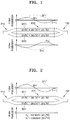
- FIG. 1 is a plan view of a non-reciprocal optical transmission device according to an example embodiment.
- a non-reciprocal optical transmission device may be an optical waveguide type device.
- the non-reciprocal optical transmission device may include an optical input portion P10 and an optical output portion P30.
- the input portion P10 may be an input terminal, and the output portion P30 may be an output terminal.
- the non-reciprocal optical transmission device may include an intermediate connecting portion P20 between the input portion P10 and the output portion P30.
- the intermediate connecting portion P20 may include optical waveguides, for example, first and second optical waveguides W10 and W20.
- the intermediate connecting portion P20 may include the first optical waveguide W10 and the second optical waveguide W20.
- either one or both of the input portion P10 and the output portion P30 may have a Y-branch structure.
- both the input portion P10 and the output portion P30 are illustrated as having the Y-branch structure.
- a complex index of refraction (or a complex refractive index) of any one or any combination of the optical waveguides W10 and W20 included in the intermediate connecting portion P20 may change between the input portion P10 and the output portion P30. Due to a change in the complex refractive index, the transmission direction of light through the non-reciprocal optical transmission device according to an example embodiment may be controlled.
- a change profile of the complex refractive index in a direction from the input portion P10 to the output portion P30 and a change profile of the complex refractive index in a direction from the output portion P30 to the input portion P10 may be asymmetric or non-symmetric with respect to the center of the intermediate connecting portion P20.
- a graph related to a change in the complex refractive index of the first optical waveguide W10 is shown above the intermediate connecting portion P20 of FIG. 1
- a graph related to a change in the complex refractive index of the second optical waveguide W20 is shown under the intermediate connecting portion P20.
- a complex refractive index of each of the first optical waveguide W10 and the second optical waveguide W20 changes between the input portion P10 and the output portion P30.
- ⁇ n 1 ' indicates a change amount of a real part of the complex refractive index of the first optical waveguide W10
- ⁇ n 1 " indicates a change amount of an imaginary part of the complex refractive index of the first optical waveguide W10.
- ⁇ n 2 ' indicates a change amount of a real part of the complex refractive index of the second optical waveguide W20
- ⁇ n 2 " indicates a change amount of an imaginary part of the complex refractive index of the second optical waveguide W20.
- the real part is related to substantial refraction of light
- the imaginary part is related to absorption of light and energy loss.
- ⁇ n 1 ' may be a first-order differential value indicating a change amount of n 1 '
- a change amount of ⁇ n 1 ' may be a second-order differential value
- ⁇ n 1 " may be a first-order differential value indicating a change amount of n 1 "
- a change amount of ⁇ n 1 " may be a second-order differential value.
- ⁇ n 2 ' and ⁇ n 2 " shown in the graph shown under the intermediate connecting portion P20. From the graph, a change tendency of ⁇ n 2 ' and ⁇ n 2 " may be seen.
- a difference between the change amount ⁇ n 1 ' of the real part of the complex refractive index of the first optical waveguide W10 and the change amount ⁇ n 2 ' of the real part of the complex refractive index of the second optical waveguide W20, that is, ⁇ n 1 '- ⁇ n 2 ', may increase and then decrease in a direction from the input portion P10 to the output portion P30 and may decrease and then increase in a direction from the output portion P30 to the input portion P10.
- the real part change amount difference may increase and then decrease, and again increase in the direction from the input portion P10 to the output portion P30, and may decrease and then increase, and again decrease in the direction from the output portion P30 to the input portion P10.
- the change graph of ⁇ n 1 ' may have an inflection point in or near the center of the intermediate connecting portion P20
- the change graph of ⁇ n 2 ' may have an inflection point in or near the center of the intermediate connecting portion P20.
- a difference between the change amount ⁇ n 1 " of the imaginary part of the complex refractive index of the first optical waveguide W10 and the change amount ⁇ n 2 " of the imaginary part of the complex refractive index of the second optical waveguide W20, that is, ⁇ n 1 "- ⁇ n 2 ", may increase and then decrease in the direction from the input portion P10 to the output portion P30.
- the imaginary part change amount difference that is, ⁇ n 1 "- ⁇ n 2 ", may increase and then decrease in the direction from the output portion P30 to the input portion P10.
- the change graph of ⁇ n 1 " and the change graph of ⁇ n 2 " may have a peak point in or near the center of the intermediate connecting portion P20.
- a change profile of the complex refractive index of the first optical waveguide W10 in the direction from the input portion P10 to the output portion P30 and a change profile of the complex refractive index of the first optical waveguide W10 in the direction from the output portion P30 to the input portion P10 may be asymmetric or non-symmetric with respect to the center of the intermediate connecting portion P20.
- a change profile of the complex refractive index of the second optical waveguide W20 in the direction from the input portion P10 to the output portion P30 and a change profile of the complex refractive index of the second optical waveguide W20 in the direction from the output portion P30 to the input portion P10 may be asymmetric or non-symmetric with respect to the center of the intermediate connecting portion P20.
- the transmission direction of light through the non-reciprocal optical transmission device may be controlled (determined). That is, light may be transmitted/propagated from the input portion P10 to the output portion P30 and may not be substantially transmitted/propagated from the output portion P30 to the input portion P10. This will be described later in more detail with reference to FIGS. 9 and 10 .
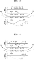
- FIG. 2 is a plan view of a non-reciprocal optical transmission device according to another example embodiment.
- an intermediate connecting portion P21 may include a first optical waveguide W11 and a second optical waveguide W21.
- the change amount ⁇ n 1 ' of the real part of the complex refractive index of the first optical waveguide W11 and the change amount ⁇ n 1 " of the imaginary part of the complex refractive index of the first optical waveguide W11 may change as shown in an upper graph.
- a real part n 2 ' and an imaginary part n 2 " of the complex refractive index of the second optical waveguide W21 may be maintained constant as shown in a lower graph.
- ⁇ n 2 ' and ⁇ n 2 " may be maintained as 0.
- the complex refractive index of the first optical waveguide W11 may change without change in the complex refractive index of the second optical waveguide W21.
- a change range of each of the change amount ⁇ n 1 ' of the real part of the complex refractive index of the first optical waveguide W11 and the change amount ⁇ n 1 " of the imaginary part of the complex refractive index of the first optical waveguide W11 may be greater than a change range of the change amount ⁇ n 1 ' of the real part of the complex refractive index of the first optical waveguide W10 and the change amount ⁇ n 1 " of the imaginary part of the complex refractive index of the first optical waveguide W10 in FIG. 1 .
- the change range of each of the change amount ⁇ n1' of the real part of the complex refractive index of the first optical waveguide W11 and the change amount ⁇ n1" of the imaginary part of the complex refractive index of the first optical waveguide W11 may be about twice greater than the change range of the change amount ⁇ n1' of the real part of the complex refractive index of the first optical waveguide W10 and the change amount ⁇ n1" of the imaginary part of the complex refractive index of the first optical waveguide W10 in FIG. 1 .
- a difference between the change amount ⁇ n 1 ' of the real part of the complex refractive index of the first optical waveguide W11 and the change amount ⁇ n 2 ' of the real part of the complex refractive index of the second optical waveguide W21, that is, ⁇ n 1 '- ⁇ n 2 ', may increase and then decrease in the direction from the input portion P10 to the output portion P30 and may decrease and then increase in the direction from the output portion P30 to the input portion P10.
- a difference between the change amount ⁇ n 1 " of the imaginary part of the complex refractive index of the first optical waveguide W11 and the change amount ⁇ n 2 " of the imaginary part of the complex refractive index of the second optical waveguide W21, that is, ⁇ n 1 "- ⁇ n 2 ", may increase and then decrease in the direction from the input portion P10 to the output portion P30.
- the non-reciprocal optical transmission device of FIG. 2 may have optical characteristics that are similar with those of the non-reciprocal optical transmission device of FIG. 1 .
- FIG. 3 is a plan view of a non-reciprocal optical transmission device according to another example embodiment.
- a change range of each of the change amount ⁇ n 2 ' of the real part of the complex refractive index of the second optical waveguide W22 and the change amount ⁇ n 2 " of the imaginary part of the complex refractive index of the second optical waveguide W22 may be, for example, twice greater than a change range of the change amount ⁇ n 2 ' of the real part of the complex refractive index of the second optical waveguide W20 and the change amount ⁇ n 1 " of the imaginary part of the complex refractive index of the second optical waveguide W20 in FIG.
- a difference between the change amount ⁇ n 1 ' of the real part of the complex refractive index of the first optical waveguide W12 and the change amount ⁇ n 2 ' of the real part of the complex refractive index of the second optical waveguide W22, that is, ⁇ n 1 ' - ⁇ n 2 ', may increase and then decrease in the direction from the input portion P10 to the output portion P30 and may decrease and then increase in the direction from the output portion P30 to the input portion P10.
- a difference between the change amount ⁇ n 1 " of the imaginary part of the complex refractive index of the first optical waveguide W12 and the change amount ⁇ n 2 " of the imaginary part of the complex refractive index of the second optical waveguide W22, that is, ⁇ n 1 "- ⁇ n 2 ", may increase and then decrease in the direction from the input portion P10 to the output portion P30.
- the non-reciprocal optical transmission device of FIG. 3 may have optical characteristics that are similar with those of the non-reciprocal optical transmission device of FIG. 1 .
- FIG. 4 is a plan view of a non-reciprocal optical transmission device according to another example embodiment.
- the real part n 1 ' of the complex refractive index of a first optical waveguide W13 changes, the imaginary part n 1 " of the complex refractive index of the first optical waveguide W13 does not change, the imaginary part n 2 " of the complex refractive index of a second optical waveguide W23 changes, and the real part n 2 ' of the complex refractive index of the second optical waveguide W23 does not change, in an intermediate connecting portion P23.
- a change in the change amount ⁇ n 1 ' of the real part of the complex refractive index of the first optical waveguide W13 may be equal to or similar to the change in ⁇ n 1 ' of FIG. 2
- a change in the change amount ⁇ n 2 " of the imaginary part of the complex refractive index of the second optical waveguide W23 may be equal to or similar to the change in ⁇ n 2 " of FIG. 3 .
- FIG. 5 is a plan view of a non-reciprocal optical transmission device according to another example embodiment.
- the imaginary part n 1 " of the complex refractive index of a first optical waveguide W14 changes, the real part n 1 ' of the complex refractive index of the first optical waveguide W14 does not change, the real part n 2 ' of the complex refractive index of a second optical waveguide W24 changes, and the imaginary part n 2 " of the complex refractive index of the second optical waveguide W24 does not change, in an intermediate connecting portion P24.
- a change in the change amount ⁇ n 1 " of the imaginary part of the complex refractive index of the first optical waveguide W14 may be equal to or similar to the change in ⁇ n 1 " of FIG. 2
- a change in the change amount ⁇ n 2 ' of the real part of the complex refractive index of the second optical waveguide W24 may be equal to or similar to the change in ⁇ n 2 ' of FIG. 3 .
- FIG. 6 is a plan view of a non-reciprocal optical transmission device according to another example embodiment.
- the real part n 1 ' and the imaginary part n 1 " of the complex refractive index of a first optical waveguide W15 change
- the real part n 2 ' of the complex refractive index of a second optical waveguide W25 changes
- the imaginary part n 2 " of the complex refractive index of the second optical waveguide W25 does not change, in an intermediate connecting portion P25.
- the changes of ⁇ n 1 ' and ⁇ n 2 ' may be equal to or similar with those of FIG. 1
- the change in ⁇ n 1 " may be equal to or similar with that of FIG. 2 .
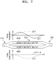
- FIG. 7 is a plan view of a non-reciprocal optical transmission device according to another example embodiment.
- the real part n 1 ' and the imaginary part n 1 " of the complex refractive index of a first optical waveguide W16 change, the real part n 2 ' of the complex refractive index of a second optical waveguide W26 does not change, and the imaginary part n 2 " of the complex refractive index of the second optical waveguide W26 changes, in an intermediate connecting portion P26.
- the changes of ⁇ n 1 " and ⁇ n 2 " may be equal to or similar with those of FIG. 1
- the change in ⁇ n 1 ' may be equal to or similar with that of FIG. 2 .
- the difference between the change amount ⁇ n 1 ' of the real part of the complex refractive index of the first optical waveguides W13 through W16 and the change amount ⁇ n 2 ' of the real part of the complex refractive index of the second optical waveguides W23 through W26, that is, ⁇ n 1 '- ⁇ n 2 ', may increase and then decrease in the direction from the input portion P10 to the output portion P30 and may decrease and then increase in the direction from the output portion P30 to the input portion P10.
- the difference between the change amount ⁇ n 1 " of the imaginary part of the complex refractive index of the first optical waveguides W13 through w16 and the change amount ⁇ n 2 " of the imaginary part of the complex refractive index of the second optical waveguides W23 through W26, that is, ⁇ n 1 " - ⁇ n 2 ", may increase and then decrease in the direction from the input portion P10 to the output portion P30.
- the non-reciprocal optical transmission devices of FIGS. 4 through 7 may have optical characteristics that are similar with those of the non-reciprocal optical transmission device of FIG. 1 .
- the imaginary part n 2 " of the complex refractive index of the second optical waveguide W25 instead of the imaginary part n 1 " of the complex refractive index of the first optical waveguide W15, may change.
- the real part n 2 ' of the complex refractive index of the second optical waveguide W26 instead of the real part n 1 ' of the complex refractive index of the first optical waveguide W16, may change.
- the first optical waveguides W10 through W16 may be regarded as second optical waveguides, or the second optical waveguides W20 through W26 may also be regarded as first optical waveguides.
- the graphs showing the changes of ⁇ n 1 ', ⁇ n 1 ", ⁇ n 2 ', and ⁇ n 2 " are examples, and may change variously.
- FIGS. 8A and 8B are graphs showing a change in a complex plane of an energy parameter ⁇ related to a plurality of optical waveguides in a non-reciprocal optical transmission device according to an example embodiment.
- FIG. 8A shows a change in an energy parameter ⁇ in a forward direction from an input portion to an output portion
- FIG. 8B shows a change in an energy parameter ⁇ in a backward direction from the output portion to the input portion.
- Re( ⁇ ) indicates a real part of the energy parameter ⁇
- Im( ⁇ ) indicates an imaginary part of the energy parameter ⁇
- EP indicates an exceptional point of an eigenvalue.
- Re( ⁇ ) and Im( ⁇ ) are related to a complex refractive index
- the eigenvalue is related to the energy parameter ⁇ .
- the energy parameter ⁇ may change to rotate in a first direction with respect to an exceptional point (EP).
- EP exceptional point
- the energy parameter ⁇ may change to rotate in a second direction with respect to the EP.
- an eigenstate of light changes, such that a phase of light between two waveguides may be switched to an asymmetric mode.
- the energy parameter ⁇ changes as shown in FIG. 8A , that is, the real part of the energy parameter ⁇ has a positive (+) value and the imaginary part thereof has a positive (+) value
- an anti-adiabatic state jump phenomenon occurs, such that the eigenstate of light does not change and the phase of light may remain in a symmetric mode.
- the anti-adiabatic state jump phenomenon does not occur during the travel of light in the backward direction, so that the eigenstate of the light changes and the phase of the light is switched to the asymmetric mode during the travel of light in the backward direction.
- the energy parameter ⁇ changes according to a circular shape around the EP in FIGS. 8A and 8B , this is an example, and the change in shape may vary.
- the energy parameter ⁇ may change according to an oval shape or a polygon shape, as well as a circular shape.
- the non-reciprocal optical transmission device may transmit light only in the forward direction and not in the backward direction.
- the physical characteristics described with reference to FIGS. 8A and 8B and a related mechanism are examples and may change.
- FIG. 9 is a schematic diagram for describing non-reciprocal optical transmission characteristics of a non-reciprocal optical transmission device according to an example embodiment.
- the non-reciprocal optical transmission device may include the input portion P1, the output portion P3, and the intermediate connection portion P2 therebetween, and the intermediate connecting portion P2 may include optical waveguides, e.g., the first optical waveguide W1 and the second optical waveguide W2.
- the non-reciprocal optical transmission device may correspond to any one of the non-reciprocal optical transmission devices of FIGS. 1 through 7 .
- FIG. 10 is a diagram showing a finite element method (FEM) simulation result with respect to a non-reciprocal optical transmission device according to an example embodiment.
- a width of two optical waveguides in an intermediate connecting portion is 1 ⁇ m
- an a distance between the two optical waveguides is 2 ⁇ m
- a length of the intermediate connecting portion is 5 mm
- a Y-branch length of each of the input portion and the output portion is 300 ⁇ m
- a wavelength of used light is 1030 nm.
- a refractive index of a part of an optical waveguide is 1.55, a variation amplitude of a complex refractive index is 0.0006, and a refractive index of a cladding layer contacting the optical waveguide is 1.5.
- the complex refractive index of the non-reciprocal optical transmission device is variated as shown in FIG. 1 .
- the non-reciprocal optical transmission device may control a transmission direction of light by using spatial variation of the complex refractive index of the optical waveguide.
- the complex refractive index may gradually change along the extending direction of the optical waveguide.
- materials or composition ratios of the optical waveguides W10 through W16 and W20 through W26 may gradually change in the longitudinal direction.
- the physical properties or characteristics of the optical waveguides W10 through W16 and W20 through W26 may gradually change.
- widths or thicknesses of the optical waveguides W10 through W16 and W20 through W26 may change in the longitudinal direction, or a side patch may be formed in adjacent to the optical waveguides W10 through W16 and W20 through W26, and a distance between the side path and the optical waveguides W10 through W16 and W20 through W26 may be adjusted, thereby changing a complex refractive index (an effective complex refractive index) of the optical waveguides W10 through W16 and W20 through W26.
- a real part i.e., an effective real part
- an effective complex refractive index of the optical waveguide may increase.
- the real part (i.e., the effective real part) of the effective complex refractive index of the optical waveguide may be adjusted.
- an imaginary part (i.e., an effective imaginary part) of the effective complex refractive index of the optical waveguide may increase.
- the imaginary part (i.e., the effective imaginary part) of the effective complex refractive index of the optical waveguide may be adjusted.
- FIG. 11A is a perspective view of a non-reciprocal optical transmission device according to another example embodiment.
- the non-reciprocal optical transmission device may include an input portion P100, an output portion P300, and an intermediate connecting portion P200 therebetween.
- the intermediate connecting portion P200 may include optical waveguides, e.g., first and second optical waveguides W100 and W200. Either one or both of the first optical waveguide W100 and the second optical waveguides W200 may undergo width and/or thickness change in a longitudinal direction thereof.
- the width of the first optical waveguide W100 gradually changes between the input portion P100 and the output portion P300.
- the width of the first optical waveguide W100 may increase and then decrease in a direction from the input portion P100 to the output portion P300 and may decrease and then increase in a direction from the output portion P300 to the input portion P100.
- a change amount of a real part (i.e., an effective real part) of an effective complex refractive index of the first optical waveguide W100 may increase and then decrease in the direction from the input portion P100 to the output portion P300 and may decrease and then increase in the direction from the output portion P300 to the input portion P100.
- the non-reciprocal optical transmission device may further include a side patch S100 provided in at least a side of the intermediate connecting portion P200.
- one side patch S100 is illustrated as being by the first optical waveguide W100.
- a distance between the first optical waveguide W100 and the side patch S100 may change between the input portion P100 and the output portion P300.
- the distance between the first optical waveguide W100 and the side patch S100 may decrease and then increase in the direction from the input portion P100 to the output portion P300.
- a change amount of an imaginary part (i.e., an effective imaginary part) of an effective complex refractive index of the first optical waveguide W100 may increase and then decrease in the direction from the input portion P100 to the output portion P300.
- the width and thickness of the second optical waveguide W200 may be maintained substantially constant between the input portion P100 and the output portion P300.
- the real part e.g., the effective real part
- the real part e.g., the effective real part
- the side patch S100 does not affect the second optical waveguide W200 and there is no second side patch adjacent to the second optical waveguide W200
- an imaginary part i.e., an effective imaginary part
- an effective complex refractive index of the second optical waveguide W200 may be maintained substantially constant between the input portion P100 and the output portion P300.
- a change in a complex refractive index of the intermediate connecting portion P200 used in the non-reciprocal optical transmission device of FIG. 11A may be equal to or similar with the change in the complex refractive index of the intermediate connecting portion P21 described with reference to FIG. 2 .
- the non-reciprocal optical transmission device of FIG. 11A may transmit light only in the forward direction, and may not transmit the light in the backward direction.
- FIG. 11B is a plan view of an intermediate connecting portion of the non-reciprocal optical transmission device of FIG. 11A , viewed from the top.
- a width w 1 of the first optical waveguide W100 changes in an x-axis direction and a width w 2 of the second optical waveguide W200 is maintained constant.
- a distance ds between the first optical waveguide W100 and the side patch S100 may change in the x-axis direction.
- an effective absorption coefficient of the first optical waveguide W100 may increase, such that a change amount of the effective imaginary part of the complex refractive index of the first optical waveguide W10 may increase.
- a distance d W between the first optical waveguide W100 and the second optical waveguide W200 may change in the x-axis direction.
- a length of the intermediate connecting portion P200 is indicated by L. Depending on the length L, characteristics and performance of the non-reciprocal optical transmission device may change.
- the first optical waveguide W100, the second optical waveguide W200, and the side patch S100 include silicon (Si)
- their thickness may be about 150 nm
- a change range of the width w 1 may be about 10 nm
- the width w 2 may be about 800 nm
- a minimum value of d S may be about 70 nm
- an average value of d W may be less than or equal to about 300 nm.
- first optical waveguide W100, the second optical waveguide W200, and the side patch S100 include a dopant-doped poly(methyl methacrylate), that is, doped PMMA
- their thickness may be about 400 nm
- a change range of the width w 1 may be about 100 nm
- the width w 2 may be about 1.2 ⁇ m
- a minimum value of d S may be about 300 nm
- an average value of d W may be less than or equal to about 1.2 ⁇ m.
- materials and related dimensions of the optical waveguides W100 and W200 and the side patch S100 are examples, and may change variously.
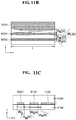
- FIG. 11C is a cross-sectional view of the intermediate connecting portion P200 of the non-reciprocal optical transmission device of FIG. 11A .
- the first optical waveguide W100, the second optical waveguide W200, and the side patch S100 may be provided on a first cladding layer C100.
- a second cladding layer C200 may be further provided to cover the first optical waveguide W100, the second optical waveguide W200, and the side patch S100.
- the first optical waveguide W100, the second optical waveguide W200, and the side patch S100 may be regarded as being embedded in the cladding layer (C100 + C200).
- the first cladding layer C100 may be an underlayer or a support layer
- the second cladding layer C200 may be an upperlayer or a cover layer.
- the first cladding layer C100 and the second cladding layer C200 may include materials having lower refractive indices than those of the first optical waveguide W100, the second optical waveguide W200, and the side patch S100.
- the first cladding layer C100 and the second cladding layer C200 may include an identical material or different materials.
- the first optical waveguide W100, the second optical waveguide W200, and the side patch S100 may include materials having refractive indices higher than those of the first cladding layer C100 and the second cladding layer C200.
- the first optical waveguide W100, the second optical waveguide W200, and the side patch S100 may include an identical material or different materials.
- the thicknesses of the first optical waveguide W100, the second optical waveguide W200, and the side patch S100 are indicated by t.
- the thickness t may be maintained substantially constant in the longitudinal direction of the first optical waveguide W100 and the second optical waveguide W200, However, according to circumstances, the thickness t of either one or both of the first optical waveguide W100 and the second optical waveguide W200 may change in the longitudinal direction of the first optical waveguide W100 and the second optical waveguide W200.
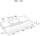
- FIG. 11D is a perspective view of a non-reciprocal optical transmission device according to another example embodiment.
- FIG. 11D is shown a case in which the structure of FIG. 11A further includes the first cladding layer C100 and the second cladding layer C200 of FIG. 11C .
- the first cladding layer C100 and the second cladding layer C200 may include a low-refractive-index material
- the first optical waveguide W100, the second optical waveguide W200, and the side patch S100 may include a high-refractive-index material.
- the low refractive index and the high refractive index may have relative concepts indicating magnification of the refractive index.
- the first optical waveguide W100, the second optical waveguide W200, and the side patch S100 of the non-reciprocal optical transmission device described with reference to FIG. 11D may include, for example, any one or any combination of a semiconductor, a polymer, a dielectric, and metal.
- the first cladding layer C100 and the second cladding layer C200 may include a dielectric such as a silicon oxide, or a polymer-based material.
- a width of each of the first optical waveguide W100 and the second optical waveguide W200 may be, for example, about 100 nm - about 100 ⁇ m.
- a width variation rate of the first optical waveguide W100 having a variable width may be, for example, about 10 nm - about 10 ⁇ m.
- a distance between the first optical waveguide W100 and the second optical waveguide W200 may be, for example, about 10 nm - about 10 ⁇ m.
- a distance between the first optical waveguide W100 and the side patch S100 may be, for example, about 1 nm - about 10 ⁇ m.
- a length of the intermediate connecting portion P200 may be, for example, about 1 ⁇ m - about 15 mm.
- An entire length of the non-reciprocal optical transmission device may be less than or equal to about 20 mm, for example.
- a thickness of the first optical waveguide W100, the second optical waveguide W200, and the side patch S100 may be, for example, about 5 nm - about 2 ⁇ m.
- the materials and related dimensions of the non-reciprocal optical transmission device may be applied to example embodiments of FIGS. 13 through 16 described later.
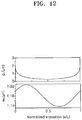
- FIG. 12 is a graph showing a change profile of the width w 1 of the first optical waveguide W100 and a change profile of the distance d S between the first optical waveguide W100 and the side patch S100 in the non-reciprocal optical transmission device described with reference to FIGS. 11A through 11D .
- w 1 increases and then decreases, and again increases in the x-axis direction.
- d S may decrease and then increase in the x-axis direction.
- the change profile of w 1 and the change profile of ds shown in FIG. 12 are examples, and their change ranges and change tendencies may vary.
- the change in the complex refractive index of the non-reciprocal optical transmission device described with reference to FIGS. 11A through 11D and 12 may be the same as or similar with that shown in FIG. 2 .
- the change in the complex refractive index of the non-reciprocal optical transmission device to be described with reference to FIG. 13 may be the same as or similar with that shown in FIG. 1 .
- FIG. 13 is a plan view of an intermediate connecting portion of a non-reciprocal optical transmission device according to another example embodiment.
- first optical waveguide W110 and a second optical waveguides W210 may undergo width and/or thickness change in a longitudinal direction thereof.
- the widths of both the first optical waveguide W110 and the second optical waveguide W210 change.
- the width of the first optical waveguide W110 may increase and then decrease in a direction from an input portion to an output portion and may decrease and then increase in a direction from the output portion to the input portion.
- the width of the second optical waveguide W210 may decrease and then increase in the direction from the input portion to the output portion, and may increase and then decrease in the direction from the output portion to the input portion.
- a distance between the first optical waveguide W110 and a first side patch S110 may decrease and then increase in the direction from the input portion to the output portion.
- a distance between the second optical waveguide W210 and a second side patch S210 may increase and then decrease in the direction from the input portion to the output portion.
- the change in the complex refractive index of the non-reciprocal optical transmission device may be the same as or similar with that shown in FIG. 1 .
- a change in the width of the first optical waveguide W100 may be about twice greater than that of the first optical waveguide W110 of FIG. 13 .
- a change in the distance between the first optical waveguide W100 and the side patch S100 may be about twice greater than that between the first optical waveguide W110 and the first side patch S110 in FIG. 13 .
- the first optical waveguides W100 and W110 are illustrated as being identical to each other and the side patches S100 and S110 are illustrated as being identical to each other in FIGS. 11B and 13 , but their changes may be different between the two example embodiments.
- the width of one W100 of the two optical waveguides W100 and W200 changes and one side patch S100 is used in FIG.
- FIGS. 14 , 15, and 16 are plan views of intermediate connecting portions of non-reciprocal optical transmission devices according to other example embodiments. These drawings show an intermediate connecting portion applicable to each non-reciprocal optical transmission device.
- a change in a complex refractive index of an intermediate connecting portion shown in FIG. 14 may correspond to the change in the complex refractive index shown in FIG. 3 .
- a width of a first optical waveguide W120 may be maintained constant, and a width of a second optical waveguide W220 may change between an input portion and an output portion.
- the width of the second optical waveguide W220 may decrease and then increase in a direction from the input portion to the output portion and may increase and then decrease in a direction from the output portion to the input portion.
- a side patch S220 may be in a side of the second optical waveguide W220, and a distance between the second optical waveguide W220 and the side patch S220 may increase and then decrease in the direction from the input portion to the output portion.
- a change in a complex refractive index of an intermediate connecting portion shown in FIG. 15 may correspond to the change in the complex refractive index shown in FIG. 4 .
- a width of a first optical waveguide W130 changes in a longitudinal direction and a width of a second optical waveguide W230 may be maintained constant.
- a side patch S230 may be in a side of the second optical waveguide W230, and a distance between the second optical waveguide W230 and the side patch S230 may increase and then decrease in the direction from the input portion to the output portion.
- a change in a complex refractive index of an intermediate connecting portion shown in FIG. 16 may correspond to the change in the complex refractive index shown in FIG. 5 .
- a width of a first optical waveguide W140 may be maintained constant, and a width of a second optical waveguide W240 may change in the longitudinal direction.
- a side patch S140 may be in a side of the first optical waveguide W140, and a distance between the first optical waveguide W140 and the side patch S140 may decrease and then increase in the direction from the input portion to the output portion.
- the non-reciprocal optical transmission device including the intermediate connecting portion corresponding to the change in the complex refractive index shown in FIGS. 6 and 7 may be designed.
- the second side patch S210 is excluded and an effect thereof is integrated into the first side patch S110 in FIG. 13 , a change in the complex refractive index as shown in FIG. 6 may be seen.
- the width of the second optical waveguide W210 is maintained constant and an effect of a change in the width of the second optical waveguide W210 is integrated into the first optical waveguide W110, a change in the complex refractive index as shown in FIG. 7 may be seen.
- various forms of non-reciprocal optical transmission devices may be designed to reflect various forms of the change in the complex refractive index modified from FIGS. 1 through 7 .
- FIG. 17 is a graph showing a measurement result of performance of a non-reciprocal optical transmission device according to an example embodiment.
- FIG. 17 includes a result of analytic calculation (model) and a result of finite element method (FEM) simulation with respect to a non-reciprocal transmission ratio (NTR) and a forward transmission efficiency (FTE).
- the results shown in FIG. 17 regard to three cases in which the length L of the intermediate connecting portion P200 in the device structured as shown in FIG. 11D is 1 mm, 5 mm, and 10 mm.
- the FEM simulation has been performed with respect to the device having the length L of 5 mm.
- a relatively high NTR (dB) may be seen in a wavelength region. As the wavelength increases, the NTR (dB) increase and then decreases. As the length L of the device (intermediate connecting portion) increases, the NTR (dB) increases.
- a change tendency of an FTE (dB) with respect to a wavelength may be seen.
- a change tendency of the FTE (dB) with respect to the length L of the device (intermediate connecting portion) may also be seen.
- the FTE (dB) is a log scale.
- the FTE (dB) of 0 (zero) means that an efficiency in a scale is 1 (out/in ratio), that is, 100%.
- Table 1 shows main characteristic parameters of the non-reciprocal optical transmission device according to an example embodiment.
- [NTR] max indicates a maximum value of NTR. If the length L is about 10 mm, a maximum value of the NTR is set, excluding a spike peak in FIG. 17 .
- ⁇ FTE> avg indicates an average value of the FTE in a scale (rate). Thus, when ⁇ FTE> avg is 1, it means that the efficiency is 100%.
- ⁇ max indicates a wavelength corresponding to the maximum value of the NTR, that is, [NTR]max.
- ⁇ 10-dB indicates a wavelength width of a region where the NTR is greater than or equal to 10 dB in the NTR (dB) graph of FIG. 17 .
- ⁇ v 10-dB is a frequency value into which ⁇ 10-dB (wavelength) is converted.
- ⁇ v 10-dB is a frequency value indicating a transmission bandwidth of a non-reciprocal optical transmission device.
- a non-reciprocal optical transmission device having a high NTR, a high FTE, and a wide transmission bandwidth may be implemented.
- the NTR may be greater than or equal to about 20 dB or about 30 dB, and the bandwidth (10dB bandwidth) may be greater than or equal to about 70 THz or about 100 THz.
- the average FTE may be about 1, such that the non-reciprocal optical transmission device according to an example embodiment may be used (almost) without signal loss.
- the non-reciprocal optical transmission device according to an example embodiment may be a chip-integration type device.
- the non-reciprocal optical transmission device may be easily manufactured on a chip or may be integrated, together with other optical elements (optical devices), in one chip. This may be meaningful in terms of ease of manufacturing and implementation of an optical chip.
- a conventional optical isolator adopts Faraday rotation occurring in a single-crystal magneto-optic medium such as yttrium-iron-garnet (YIG) crystals, etc.
- a single-crystal magneto-optic medium such as yttrium-iron-garnet (YIG) crystals, etc.
- YIG yttrium-iron-garnet
- a length of a device based on the single-crystal magneto-optical medium is about 5 cm to about 10 cm, and a cross-sectional area of the device is about several cm 2 , such that the device is difficult to insert into high-integration optical apparatus and system.
- performance such as the NTR, the FTE, the bandwidth, etc., there is a limitation in implementation of excellent performance.
- the device based on the single-crystal magneto-optic medium there are an Si waveguide resonator device to which a poly-crystal magneto-optic medium thin film is applied, a waveguide diffraction grating device using indirect interband photonic transition, a nonlinear asymmetric waveguide/photonic crystal resonator device, etc., but all of these techniques have narrow bandwidths of about 100 GHz or less and low FTEs, and in some cases, a high-power light source may have to be used, making it difficult to implement devices at practical levels.
- the Si waveguide resonator device to which the poly-crystal magneto-optic medium thin film is applied has a narrow bandwidth ( ⁇ 2 GHz) and a low FTE ( ⁇ 1%).
- the waveguide diffraction grating device using indirect interband photonic transition has a low NTR ( ⁇ 3dB), and a high-power (equivalent to 0.1W) ultra-high-frequency acoustic wave or electro-optic traveling wave generator in a 10 GHz band also has to be integrated together with the waveguide device.
- the nonlinear asymmetric waveguide/photonic crystal resonator device has a narrow bandwidth ( ⁇ 100 GHz) and a low FTE ( ⁇ 10%), and operates only for a high-power optical signal.
- the non-reciprocal optical transmission device may be easily manufactured on a chip, while easily guaranteeing excellent performance such as a high NTR, a high FTE, a wide bandwidth, and so forth.
- excellent performance such as a high NTR, a high FTE, a wide bandwidth, and so forth.
- an FTE of about 90% or higher and a bandwidth of about 100 THz or wider may be implemented, and a low-power operation may be possible.
- the non-reciprocal optical transmission device according to an example embodiment uses variation of a complex refractive index without depending on a resonance cavity or a beat phenomenon, thus implementing a very wide bandwidth (about 100 THz or wider).
- the non-reciprocal optical transmission device may be used in an optical integrated circuit device for next-generation 10 THz or 100 THz-class ultra wideband/ultra high-density digital information processing.
- Various non-reciprocal optical devices proposed conventionally have limitations and problems such as narrow band characteristics, a low forward transmission efficiency, a need for a non-realistic ultra-high-frequency acoustic wave generator, operability only for high-power optical waves, impossibility of integration, and so forth.
- the non-reciprocal optical transmission device may overcome such limitations and problems, thus being applied to implementation of next-generation digital optical information processing apparatuses and systems.
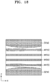
- FIG. 18 is a plan view of an intermediate connecting portion of a non-reciprocal optical transmission device according to another example embodiment.
- an intermediate connecting portion may include a first optical waveguide W150, a second optical waveguide W250, a third optical waveguide W350, and a fourth optical waveguide W450.
- a width of any one or any combination of the first through fourth optical waveguides W150 through W450 may change in the direction from the input portion to the output portion.
- the widths of the first optical waveguide W150 and the fourth optical waveguide W450 change. Widths of the second optical waveguide W250 and the third optical waveguide W350 may be maintained constant, without substantially (globally) changing.
- a first side patch S150 may be further provided in a side of the first optical waveguide W150.
- a second side patch S250 may be further provided in a side of the fourth optical waveguide W450.
- a distance between the first optical waveguide W150 and the first side patch S150 may change between the input portion and the output portion.
- a distance between the fourth optical waveguide W450 and a second side patch S250 may change between the input portion and the output portion.
- Structures of the first optical waveguide W150, the second optical waveguide W250, and the first side patch S150 may be similar with those of the first optical waveguide W100, the second optical waveguide W200, and the side patch S100 of FIG. 11B .
- Structures of the third optical waveguide W350, the fourth optical waveguide W450, and the second side patch S250 may be symmetric to those of the first optical waveguide W150, the second optical waveguide W250, and the side patch S150.
- forms of the first through fourth optical waveguides W150 through W450 described in FIG. 18 and forms of the first side patch S150 and the second side patch S250 are examples, and may change variously.
- the structure of FIG.18 may be modified variously.
- an input portion connected to them may be provided, and in the other side of each of the plurality of optical waveguides W150 through W450, an output portion connected to them may be provided.
- Each of the input portion and the output portion may include four branches.
- the number of optical waveguides included in an intermediate connecting portion may be equal to 3 or greater than or equal to 5.
- a side patch may be provided between a plurality of optical waveguides.
- the thickness of the optical waveguide instead of the width of the optical waveguide may change.
- the change tendency of the thickness of the optical waveguide in the longitudinal direction may be similar with that of the width.
- both the width and the thickness of the optical waveguide may change together.
- the width/thickness change (i.e., volume change) of the optical waveguide and the adjustment of the distance between the optical waveguide and the side patch may not be used together.
- an effect of the side patch may be implemented in other ways, without using the side patch.
- an effect of the width/thickness change in the optical waveguide may be implemented in other ways, without changing the width/thickness of the optical waveguide.
- the non-reciprocal optical transmission device may be applied to optical devices in various fields.
- FIG. 19 is a perspective view of an optical apparatus to which a non-reciprocal optical transmission device is applied, according to an example embodiment.
- a non-reciprocal optical transmission element E2 according to an example embodiment is provided on a substrate SUB1.
- the non-reciprocal optical transmission element E2 may correspond to the non-reciprocal optical transmission devices that have been described with reference to FIGS. 1 through 18 .
- the non-reciprocal optical transmission element E2 may be a sort of optical isolator.
- An input terminal connecting optical element E1 for inputting light to an input portion of the non-reciprocal optical transmission element E2 may be provided.
- An output terminal connecting optical element E3 for receiving light output from an output portion of the non-reciprocal optical transmission element E2 may be further provided.
- the input terminal connecting optical element E1 and the output terminal connecting optical element E3 may be provided, together with the non-reciprocal optical transmission element E2, on the identical substrate SUB1.
- the input terminal connecting optical element E1 may include, for example, a light source.
- the light source may be a laser source or other light sources.
- the output terminal connecting optical element E3 may include a waveguide and an optical component. At least one other optical element connected to the output terminal connecting optical element E3 may be further provided on the substrate SUB1.
- a non-reciprocal optical transmission device may be applied to a light detection and ranging (LiDAR) apparatus.
- LiDAR light detection and ranging
- a non-reciprocal optical transmission device according to an example embodiment is applied to a beam steering device of the LiDAR apparatus.
- FIG. 20 is a cross-sectional view of a beam steering device to which a non-reciprocal optical transmission device is applied, according to an example embodiment.
- the beam steering device may include an input optical element E10 and an output optical element E50 provided on a substrate SUB10.
- the input optical element E10 may be a light source or an input coupler that receives light from an external light source.
- the output optical element E50 may be an emitter that emits light.
- the output optical element E50 may be a sort of output coupler.
- the beam steering device may further include a non-reciprocal optical transmission element E20, an optical splitter E30, and an optical modulator E40 between the input optical element E10 and the output optical element E50.
- the non-reciprocal optical transmission element E20 may correspond to the non-reciprocal optical transmission devices that have been described with reference to FIGS. 1 through 18 .
- the optical splitter E30 splits light delivered from the non-reciprocal optical transmission element E20 into a plurality of lights.
- the optical modulator E40 modulates the plurality of split lights.
- a direction of light (i.e., an emitted light) emitted from the output optical element E50 may be controlled by the modulation of the light in the optical modulator E40.
- An insulating layer N10 is optionally provided on a substrate SUB10, and the input optical element E10, the non-reciprocal optical transmission element E20, the optical splitter E30, the optical modulator E40, and the output optical element E50 may be provided on the insulating layer N10.
- the input optical element E10, the non-reciprocal optical transmission element E20, the optical splitter E30, the optical modulator E40, and the output optical element E50 are illustrated as simple structures.
- Optical waveguide(s) may be provided between two adjacent elements, i.e., between the input optical element E10 and the non-reciprocal optical transmission element E20, between the non-reciprocal optical transmission element E20 and the optical splitter E30, between the optical splitter E30 and the optical modulator E40, and between the optical modulator E40 and the output optical element E50.
- a cover layer C10 may be further provided to cover the input optical element E10, the non-reciprocal optical transmission element E20, the optical splitter E30, the optical modulator E40, and the output optical element E50.
- the cover layer C10 may include a low-index material having a low refractive index.
- the cover layer C10 may include a dielectric such as a silicon oxide, or a polymer-based material.
- the cover layer C10 may also serve as a sort of protective layer. However, in some cases, the cover layer C10 may not be used.
- any one or any combination of the input optical element E10, the non-reciprocal optical transmission element E20, the optical splitter E30, the optical modulator E40, and the output optical element E50 may include any one or any combination of a semiconductor, a polymer, a dielectric, and metal.
- any one or any combination of the input optical element E10, the non-reciprocal optical transmission element E20, the optical splitter E30, the optical modulator E40, and the output optical element E50 may include any one or any combination of an IV-group material (e.g., Si, Ge, etc.), a compound including an IV-group material (e.g., SiGe, etc.), an III-V-group compound, an oxide, a nitride, and a polymer.
- at least two of the input optical element E10, the non-reciprocal optical transmission element E20, the optical splitter E30, the optical modulator E40, and the output optical element E50 may include different materials.
- the beam steering device may be implemented/manufactured using a technique in the field of "silicon photonics."
- the silicon photonics technique may be used for ease of processing because the silicon photonics technique may be used (i.e., compatible) with complementary metal oxide semiconductor (CMOS) processing.
- CMOS complementary metal oxide semiconductor
- FIG. 21 is a block diagram of an overall system of an optical apparatus A1 including a beam steering device to which a non-reciprocal optical transmission device is applied, according to an example embodiment.
- An optical apparatus A1 may be a LiDAR apparatus.
- the optical apparatus A1 may include a beam steering device 1000.
- the beam steering device 1000 may include a non-reciprocal optical transmission device according to an example embodiment, and for example, may have a device structure described with reference to FIG. 20 .
- the optical apparatus A1 may include a light source in the beam steering device 1000 or may include a light source provided separately from the beam steering device 1000.
- the optical apparatus A1 may include a detector 2000 that detects light that is steered by the beam steering device 1000 and then reflected by an object.
- the detector 2000 may include an optical receiver.
- the detector 2000 may further include a filter or other optical members.
- the optical apparatus A1 may further include a circuit 3000 connected to either one or both of the beam steering device 1000 and the detector 2000.
- the circuit 3000 may include a calculator (processor) that obtains and calculates data, and may further include a driver, a controller, and so forth.
- the circuit 3000 may further include a power source, a memory, and so forth.
- the optical apparatus A1 is illustrated as including the beam steering device 1000 and the detector 2000 in one apparatus in FIG. 21
- the beam steering device 1000 and the detector 2000 may be separately provided in separate apparatuses, instead of being provided in one apparatus.
- the circuit 3000 may be connected to the beam steering device 1000 or the detector 2000 through wireless communication, instead of wired communication.
- the structure shown in FIG. 21 may change variously.
- An optical apparatus may be a LiDAR apparatus.
- the LiDAR apparatus may be of a time-of-flight (TOF) or phase-shift type.
- the LiDAR apparatus may be applied to an autonomous vehicle, a flying object like a drone, etc., a mobile device, a small walking means (e.g., a bicycle, a motorcycle, a stroller, a board, etc.), robots, assisting means for humans/animals (e.g., a cane, a helmet, an ornament, a watch, a bag, etc.), an Internet of things (loT) apparatus/system, a security apparatus/system, and so forth.
- a small walking means e.g., a bicycle, a motorcycle, a stroller, a board, etc.
- robots assisting means for humans/animals (e.g., a cane, a helmet, an ornament, a watch, a bag, etc.)
- an Internet of things (loT) apparatus/system
- the beam steering device and the optical apparatus including the same according to an example embodiment may be applied to an apparatus for obtaining a three-dimensional (3D) image, a 3D camera, etc.
- the beam steering device and the optical apparatus including the same according to an example embodiment may be applied to various optical and electronic device fields for various purposes.
- the non-reciprocal optical transmission device according to an example embodiment is applicable to other various optical apparatuses as well as the beam steering device or the LiDAR apparatus.
- the non-reciprocal optical transmission device may be applied to various health care apparatuses including a mobile health care apparatus.
- FIG. 22 is a diagram showing an integrated optical processor to which a non-reciprocal optical transmission device is applied, according to an example embodiment.
- an integrated optical processor may include a non-reciprocal optical transmission device E200 according to an example embodiment.
- the non-reciprocal optical transmission device E200 may be a sort of on-chip optical isolator.
- a light source E100 for inputting light to the non-reciprocal optical transmission device E200 may be provided.
- a bus waveguide extending from the non-reciprocal optical transmission device E200 may be provided.
- the non-reciprocal optical transmission device may be applied to any optical device based on a nonlinear effect as well as an apparatus using a laser light source.
- Optical devices based on the non-linear effect may include an optical logical operation device, a wavelength conversion device, an optical amplifier, an optical buffer, a high-order harmonic generation device, and so forth.
- the non-reciprocal optical transmission device may be applied to an optical diode, an optical circulator, etc., as well as an optical isolator.
- the non-reciprocal optical transmission device may be manufactured on various substrates.
- the non-reciprocal optical transmission device may be manufactured on a semiconductor substrate, an insulating substrate, or a conductive substrate. If the semiconductor substrate is used, a general semiconductor substrate, a semiconductor-on-insulator (SOI) substrate, a semiconductor-on-glass (SOG) substrate, etc., may be used.
- SOI semiconductor-on-insulator
- SOG semiconductor-on-glass
- a non-reciprocal optical transmission device may be manufactured from the amorphous semiconductor layer.
- the method of manufacturing the non-reciprocal optical transmission device using the SOI substrate may be as shown in FIGS. 23A through 23D .
- FIGS. 23A, 23B , 23C, and 23D are cross-sectional views showing a method of manufacturing a non-reciprocal optical transmission device according to an example embodiment.
- an insulating layer 110 may be provided on a first substrate 100, and a semiconductor layer 120 may be provided on the insulating layer 110.
- the first substrate 100 may be a semiconductor substrate.
- the first substrate 100, the insulating layer 110, and the semiconductor layer 120 may form one SOI substrate.
- the insulating layer 110 may be a dielectric or a polymer.
- the semiconductor layer 120 may include any one or any combination of various semiconductors such as Si, Ge, SiGe, etc.
- a plurality of optical waveguides 120a and 120b may be formed from the semiconductor layer 120 by patterning the semiconductor layer 120.
- the first optical waveguide 120a and the second optical waveguide 120b may be formed.
- at least one side patch 120c may be further formed from the semiconductor layer 120.
- the first optical waveguide 120a, the second optical waveguide 120b, and the side patch 120c may correspond to the first optical waveguide W100, the second optical waveguide W200, and the side patch S100 described with reference to FIG. 11A .
- a cladding layer 130 may be formed to cover the first optical waveguide 120a, the second optical waveguide 120b, and the side patch 120c.
- the cladding layer 130 may be formed of a dielectric or a polymer.
- the first substrate 100 on which the cladding layer 130 is formed may be bonded to a second substrate 200.
- One surface of the cladding layer 130 may be bonded to one surface of the second substrate 200.
- the cladding layer 130 may be provided between the first substrate 100 and the second substrate 200.
- a bonding layer 210 may be provided between the second substrate 200 and the cladding layer 130.
- the bonding layer 210 may include a polymer, metal, etc. In some cases, the bonding layer 210 may not be used.
- the first substrate 100 may be removed/separated from a structure (a deposited structure) shown in FIG. 23C .
- a resultant is shown in FIG. 23D .
- the cladding layer 130 may be provided on the second substrate 200, and the first optical waveguide W100, the second optical waveguide W200, and the side patch S100 may be provided in the cladding layer 130.
- an insulating layer 110 may be provided to cover the first optical waveguide W100, the second optical waveguide W200, and the side patch S100.
- the insulating layer 110 may be an upper cladding layer.
- the method of manufacturing the non-reciprocal optical transmission device described with reference to FIGS. 23A through 23D is an example, and may change variously.
- the method may change variously according to a material of a substrate, a material of an optical waveguide, and so forth.
- a transfer process as performed in FIGS. 23A through 23D may not be used.
- at least one optical element optically connected thereto may be further formed to manufacture various optical apparatuses.
Landscapes
- Physics & Mathematics (AREA)
- General Physics & Mathematics (AREA)
- Optics & Photonics (AREA)
- Nonlinear Science (AREA)
- Engineering & Computer Science (AREA)
- Power Engineering (AREA)
- Microelectronics & Electronic Packaging (AREA)
- Optical Integrated Circuits (AREA)
Applications Claiming Priority (1)
| Application Number | Priority Date | Filing Date | Title |
|---|---|---|---|
| KR1020160184358A KR102703715B1 (ko) | 2016-12-30 | 2016-12-30 | 비가역 광투과 소자 및 이를 포함하는 광학 장치 |
Publications (2)
| Publication Number | Publication Date |
|---|---|
| EP3343254A1 true EP3343254A1 (fr) | 2018-07-04 |
| EP3343254B1 EP3343254B1 (fr) | 2023-01-18 |
Family
ID=59676950
Family Applications (1)
| Application Number | Title | Priority Date | Filing Date |
|---|---|---|---|
| EP17183390.8A Active EP3343254B1 (fr) | 2016-12-30 | 2017-07-26 | Dispositif de transmission optique non réciproque et appareil optique comprenant celui-ci |
Country Status (4)
| Country | Link |
|---|---|
| US (2) | US10670891B2 (fr) |
| EP (1) | EP3343254B1 (fr) |
| KR (1) | KR102703715B1 (fr) |
| CN (1) | CN108267814B (fr) |
Families Citing this family (6)
| Publication number | Priority date | Publication date | Assignee | Title |
|---|---|---|---|---|
| KR102703715B1 (ko) * | 2016-12-30 | 2024-09-05 | 삼성전자주식회사 | 비가역 광투과 소자 및 이를 포함하는 광학 장치 |
| WO2020219554A1 (fr) | 2019-04-23 | 2020-10-29 | Regents Of The University Of Minnesota | Isolateurs photoniques à gyrotropie élevés directement sur un substrat |
| US12055756B2 (en) | 2019-10-14 | 2024-08-06 | Regents Of The University Of Minnesota | Push-pull non-reciprocal phase shifting |
| CN113671630B (zh) * | 2021-07-14 | 2022-11-08 | 电子科技大学 | 一种基于硅基集成的平面超透镜结构非互易光路由器 |
| KR102898220B1 (ko) * | 2023-10-11 | 2025-12-09 | 주식회사 포토니솔 | 편광 모드 제어형 비가역 광 도파로 소자 및 이를 이용한 광 아이솔레이터 및 광 서큘레이터 소자 |
| CN119620503B (zh) * | 2024-12-25 | 2025-10-10 | 南京信息工程大学 | 一种基于光学非线性及pt对称原理的非互易光传输装置 |
Citations (2)
| Publication number | Priority date | Publication date | Assignee | Title |
|---|---|---|---|---|
| EP0952472A2 (fr) * | 1998-04-21 | 1999-10-27 | Kabushiki Kaisha Toshiba | Elément fonctionnel optique et dispositif transmetteur |
| US20040081398A1 (en) * | 2000-07-31 | 2004-04-29 | 3849988 Canada Inc. | Optical waveguide filters |
Family Cites Families (22)
| Publication number | Priority date | Publication date | Assignee | Title |
|---|---|---|---|---|
| JPH1068910A (ja) | 1996-02-28 | 1998-03-10 | Nippon Telegr & Teleph Corp <Ntt> | 光非相反回路 |
| US5905823A (en) | 1996-02-28 | 1999-05-18 | Nippon Telegraph And Telephone Corporation | Polarization independent optical nonreciprocal circuit based on even mode to odd mode conversion |
| CN1184945A (zh) * | 1997-12-26 | 1998-06-17 | 清华大学 | 一种全光纤的非互易传输方法与全光纤隔离器 |
| EP1050773A1 (fr) * | 1999-05-04 | 2000-11-08 | Corning Incorporated | Dispositif commutateur piézoélectrique optique |
| US6438280B1 (en) * | 1999-12-23 | 2002-08-20 | Litton Systems, Inc. | Integrated optics chip having reduced surface wave propagation |
| US6943932B2 (en) | 2000-04-20 | 2005-09-13 | The Trustees Of Columbia University In The City Of New York | Waveguide mach-zehnder optical isolator utilizing transverse magneto-optical phase shift |
| AU2003296113A1 (en) * | 2002-12-26 | 2004-07-22 | Nippon Telegraph And Telephone Corporation | Wave transmission medium and waveguide circuit |
| US7065265B2 (en) | 2003-05-12 | 2006-06-20 | Photodigm, Inc. | Ferromagnetic-semiconductor composite isolator and method |
| EP1653260A1 (fr) * | 2003-07-18 | 2006-05-03 | Nippon Sheet Glass Co.,Ltd. | Guide d'ondes a cristal photonique, guide d'ondes a milieu homogene et dispositif optique |
| KR100580658B1 (ko) | 2004-12-24 | 2006-05-16 | 삼성전자주식회사 | 광 결정을 이용한 광 아이솔레이터 |
| US7260281B2 (en) | 2005-03-30 | 2007-08-21 | Intel Corporation | Integratable optical isolator in a Mach-Zehnder interferometer configuration |
| JP2007114222A (ja) * | 2005-03-31 | 2007-05-10 | Sumitomo Osaka Cement Co Ltd | 光制御素子 |
| CN100371775C (zh) * | 2006-04-10 | 2008-02-27 | 浙江大学 | 波导型非互易光分束器件 |
| JPWO2009078248A1 (ja) * | 2007-12-14 | 2011-04-28 | 日本電気株式会社 | 導波路型光デバイス |
| WO2009081488A1 (fr) * | 2007-12-25 | 2009-07-02 | Shibaura Institute Of Technology | Dispositif optique non réciproque et procédé de fabrication du dispositif optique non réciproque |
| US8842942B2 (en) * | 2010-02-08 | 2014-09-23 | Samsung Electronics Co., Ltd. | Optical modulator formed on bulk-silicon substrate |
| JP5515927B2 (ja) * | 2010-03-24 | 2014-06-11 | 住友電気工業株式会社 | 半導体光素子 |
| JP5891834B2 (ja) * | 2012-02-17 | 2016-03-23 | 住友電気工業株式会社 | 半導体変調器および半導体変調器の出力パワー制御方法 |
| CN103472536B (zh) * | 2013-08-16 | 2015-07-01 | 上海交通大学 | Mach-Zehder干涉仪结构的硅基光隔离器 |
| KR101751704B1 (ko) | 2014-12-30 | 2017-06-30 | 광주과학기술원 | 광 아이솔레이터 |
| CN104977733B (zh) * | 2015-05-12 | 2021-09-14 | 桂林 | 一种硅基非互易器件结构与电控非互易实现方法 |
| KR102703715B1 (ko) * | 2016-12-30 | 2024-09-05 | 삼성전자주식회사 | 비가역 광투과 소자 및 이를 포함하는 광학 장치 |
-
2016
- 2016-12-30 KR KR1020160184358A patent/KR102703715B1/ko active Active
-
2017
- 2017-06-26 US US15/632,640 patent/US10670891B2/en active Active
- 2017-07-26 EP EP17183390.8A patent/EP3343254B1/fr active Active
- 2017-12-07 CN CN201711283653.5A patent/CN108267814B/zh active Active
-
2020
- 2020-04-24 US US16/857,756 patent/US11262606B2/en active Active
Patent Citations (2)
| Publication number | Priority date | Publication date | Assignee | Title |
|---|---|---|---|---|
| EP0952472A2 (fr) * | 1998-04-21 | 1999-10-27 | Kabushiki Kaisha Toshiba | Elément fonctionnel optique et dispositif transmetteur |
| US20040081398A1 (en) * | 2000-07-31 | 2004-04-29 | 3849988 Canada Inc. | Optical waveguide filters |
Also Published As
| Publication number | Publication date |
|---|---|
| US20180188559A1 (en) | 2018-07-05 |
| EP3343254B1 (fr) | 2023-01-18 |
| KR102703715B1 (ko) | 2024-09-05 |
| CN108267814A (zh) | 2018-07-10 |
| US10670891B2 (en) | 2020-06-02 |
| KR20180079009A (ko) | 2018-07-10 |
| US11262606B2 (en) | 2022-03-01 |
| US20200257142A1 (en) | 2020-08-13 |
| CN108267814B (zh) | 2021-03-19 |
Similar Documents
| Publication | Publication Date | Title |
|---|---|---|
| EP3343254B1 (fr) | Dispositif de transmission optique non réciproque et appareil optique comprenant celui-ci | |
| US6853479B1 (en) | Apparatus and method for coupling light between an optical resonator and a semiconductor chip with a minimum number of components and alignment steps | |
| CN113777708A (zh) | 模变换器 | |
| CN101320111B (zh) | 并行模式变换器和由其构成的光分路器 | |
| JP2021032997A (ja) | トポロジカル光回路 | |
| US11733455B2 (en) | Amplitude and phase light modulator based on miniature optical resonators | |
| WO2015163958A2 (fr) | Méta-matériaux d'indice nul photoniques à adaptation d'impédance intégrés | |
| EP3164746B1 (fr) | Coupleur optique a double pointe | |
| JP2003177369A (ja) | 半導体光変調器、それを用いたマッハツェンダ型光変調器、及び半導体光変調器の製造方法 | |
| WO2020202608A1 (fr) | Élément et dispositif de guide d'onde optique | |
| US20200363584A1 (en) | Isolator, light source device, optical transmitter, and optical amplifier | |
| US11841598B2 (en) | Optical modulator | |
| CN107592915A (zh) | 慢光生成光学装置以及产生低损耗慢光的方法 | |
| WO2019159345A1 (fr) | Dispositif optique intégré à semi-conducteur | |
| JP2708119B2 (ja) | 単一モード光導波装置 | |
| US20080180340A1 (en) | Waveguide Coupling Devices | |
| Gao et al. | Integrated contra-directionally coupled chirped Bragg grating waveguide with a linear group delay spectrum | |
| CN217484626U (zh) | 相位调制器 | |
| Wang et al. | A waveguide-integrated graphene-based subwavelength electro-optic switch at 1550 nm | |
| US20050196092A1 (en) | Optical modulator and communications system | |
| US20110194801A1 (en) | Optical device using negative goos-hanchen shift | |
| US12482951B2 (en) | Dielectric waveguide, terahertz circuit and terahertz integrated circuit | |
| Sato et al. | In-plane light propagation in Ta/sub 2/O/sub 5//SiO/sub 2/autocloned photonic crystals | |
| Mynbaev et al. | Plasmonic-based devices for optical communications | |
| Davidovich et al. | Waves in active and dissipative flat-layered periodic and pseudo-periodic structures |
Legal Events
| Date | Code | Title | Description |
|---|---|---|---|
| PUAI | Public reference made under article 153(3) epc to a published international application that has entered the european phase |
Free format text: ORIGINAL CODE: 0009012 |
|
| STAA | Information on the status of an ep patent application or granted ep patent |
Free format text: STATUS: THE APPLICATION HAS BEEN PUBLISHED |
|
| AK | Designated contracting states |
Kind code of ref document: A1 Designated state(s): AL AT BE BG CH CY CZ DE DK EE ES FI FR GB GR HR HU IE IS IT LI LT LU LV MC MK MT NL NO PL PT RO RS SE SI SK SM TR |
|
| AX | Request for extension of the european patent |
Extension state: BA ME |
|
| STAA | Information on the status of an ep patent application or granted ep patent |
Free format text: STATUS: REQUEST FOR EXAMINATION WAS MADE |
|
| 17P | Request for examination filed |
Effective date: 20190104 |
|
| RBV | Designated contracting states (corrected) |
Designated state(s): AL AT BE BG CH CY CZ DE DK EE ES FI FR GB GR HR HU IE IS IT LI LT LU LV MC MK MT NL NO PL PT RO RS SE SI SK SM TR |
|
| STAA | Information on the status of an ep patent application or granted ep patent |
Free format text: STATUS: EXAMINATION IS IN PROGRESS |
|
| 17Q | First examination report despatched |
Effective date: 20200630 |
|
| GRAP | Despatch of communication of intention to grant a patent |
Free format text: ORIGINAL CODE: EPIDOSNIGR1 |
|
| STAA | Information on the status of an ep patent application or granted ep patent |
Free format text: STATUS: GRANT OF PATENT IS INTENDED |
|
| INTG | Intention to grant announced |
Effective date: 20220801 |
|
| RIN1 | Information on inventor provided before grant (corrected) |
Inventor name: LEE, CHANGSEUNG Inventor name: LEE, JEONGYUB Inventor name: KIM, YONGSUNG Inventor name: HAN, CHOLOONG Inventor name: YOON, JAEWOONG Inventor name: SONG, SEOKHO Inventor name: CHOI, YOUNGSUN Inventor name: YANG, KIYEON |
|
| GRAS | Grant fee paid |
Free format text: ORIGINAL CODE: EPIDOSNIGR3 |
|
| GRAA | (expected) grant |
Free format text: ORIGINAL CODE: 0009210 |
|
| STAA | Information on the status of an ep patent application or granted ep patent |
Free format text: STATUS: THE PATENT HAS BEEN GRANTED |
|
| AK | Designated contracting states |
Kind code of ref document: B1 Designated state(s): AL AT BE BG CH CY CZ DE DK EE ES FI FR GB GR HR HU IE IS IT LI LT LU LV MC MK MT NL NO PL PT RO RS SE SI SK SM TR |
|
| REG | Reference to a national code |
Ref country code: GB Ref legal event code: FG4D |
|
| REG | Reference to a national code |
Ref country code: CH Ref legal event code: EP |
|
| REG | Reference to a national code |
Ref country code: DE Ref legal event code: R096 Ref document number: 602017065540 Country of ref document: DE |
|
| REG | Reference to a national code |
Ref country code: AT Ref legal event code: REF Ref document number: 1545015 Country of ref document: AT Kind code of ref document: T Effective date: 20230215 Ref country code: IE Ref legal event code: FG4D |
|
| REG | Reference to a national code |
Ref country code: LT Ref legal event code: MG9D |
|
| REG | Reference to a national code |
Ref country code: NL Ref legal event code: MP Effective date: 20230118 |
|
| REG | Reference to a national code |
Ref country code: AT Ref legal event code: MK05 Ref document number: 1545015 Country of ref document: AT Kind code of ref document: T Effective date: 20230118 |
|
| PG25 | Lapsed in a contracting state [announced via postgrant information from national office to epo] |
Ref country code: NL Free format text: LAPSE BECAUSE OF FAILURE TO SUBMIT A TRANSLATION OF THE DESCRIPTION OR TO PAY THE FEE WITHIN THE PRESCRIBED TIME-LIMIT Effective date: 20230118 |
|
| P01 | Opt-out of the competence of the unified patent court (upc) registered |
Effective date: 20230530 |
|
| PG25 | Lapsed in a contracting state [announced via postgrant information from national office to epo] |
Ref country code: RS Free format text: LAPSE BECAUSE OF FAILURE TO SUBMIT A TRANSLATION OF THE DESCRIPTION OR TO PAY THE FEE WITHIN THE PRESCRIBED TIME-LIMIT Effective date: 20230118 Ref country code: PT Free format text: LAPSE BECAUSE OF FAILURE TO SUBMIT A TRANSLATION OF THE DESCRIPTION OR TO PAY THE FEE WITHIN THE PRESCRIBED TIME-LIMIT Effective date: 20230518 Ref country code: NO Free format text: LAPSE BECAUSE OF FAILURE TO SUBMIT A TRANSLATION OF THE DESCRIPTION OR TO PAY THE FEE WITHIN THE PRESCRIBED TIME-LIMIT Effective date: 20230418 Ref country code: LV Free format text: LAPSE BECAUSE OF FAILURE TO SUBMIT A TRANSLATION OF THE DESCRIPTION OR TO PAY THE FEE WITHIN THE PRESCRIBED TIME-LIMIT Effective date: 20230118 Ref country code: LT Free format text: LAPSE BECAUSE OF FAILURE TO SUBMIT A TRANSLATION OF THE DESCRIPTION OR TO PAY THE FEE WITHIN THE PRESCRIBED TIME-LIMIT Effective date: 20230118 Ref country code: HR Free format text: LAPSE BECAUSE OF FAILURE TO SUBMIT A TRANSLATION OF THE DESCRIPTION OR TO PAY THE FEE WITHIN THE PRESCRIBED TIME-LIMIT Effective date: 20230118 Ref country code: ES Free format text: LAPSE BECAUSE OF FAILURE TO SUBMIT A TRANSLATION OF THE DESCRIPTION OR TO PAY THE FEE WITHIN THE PRESCRIBED TIME-LIMIT Effective date: 20230118 Ref country code: AT Free format text: LAPSE BECAUSE OF FAILURE TO SUBMIT A TRANSLATION OF THE DESCRIPTION OR TO PAY THE FEE WITHIN THE PRESCRIBED TIME-LIMIT Effective date: 20230118 |
|
| PG25 | Lapsed in a contracting state [announced via postgrant information from national office to epo] |
Ref country code: SE Free format text: LAPSE BECAUSE OF FAILURE TO SUBMIT A TRANSLATION OF THE DESCRIPTION OR TO PAY THE FEE WITHIN THE PRESCRIBED TIME-LIMIT Effective date: 20230118 Ref country code: PL Free format text: LAPSE BECAUSE OF FAILURE TO SUBMIT A TRANSLATION OF THE DESCRIPTION OR TO PAY THE FEE WITHIN THE PRESCRIBED TIME-LIMIT Effective date: 20230118 Ref country code: IS Free format text: LAPSE BECAUSE OF FAILURE TO SUBMIT A TRANSLATION OF THE DESCRIPTION OR TO PAY THE FEE WITHIN THE PRESCRIBED TIME-LIMIT Effective date: 20230518 Ref country code: GR Free format text: LAPSE BECAUSE OF FAILURE TO SUBMIT A TRANSLATION OF THE DESCRIPTION OR TO PAY THE FEE WITHIN THE PRESCRIBED TIME-LIMIT Effective date: 20230419 Ref country code: FI Free format text: LAPSE BECAUSE OF FAILURE TO SUBMIT A TRANSLATION OF THE DESCRIPTION OR TO PAY THE FEE WITHIN THE PRESCRIBED TIME-LIMIT Effective date: 20230118 |
|
| REG | Reference to a national code |
Ref country code: DE Ref legal event code: R097 Ref document number: 602017065540 Country of ref document: DE |
|
| PG25 | Lapsed in a contracting state [announced via postgrant information from national office to epo] |
Ref country code: SM Free format text: LAPSE BECAUSE OF FAILURE TO SUBMIT A TRANSLATION OF THE DESCRIPTION OR TO PAY THE FEE WITHIN THE PRESCRIBED TIME-LIMIT Effective date: 20230118 Ref country code: RO Free format text: LAPSE BECAUSE OF FAILURE TO SUBMIT A TRANSLATION OF THE DESCRIPTION OR TO PAY THE FEE WITHIN THE PRESCRIBED TIME-LIMIT Effective date: 20230118 Ref country code: EE Free format text: LAPSE BECAUSE OF FAILURE TO SUBMIT A TRANSLATION OF THE DESCRIPTION OR TO PAY THE FEE WITHIN THE PRESCRIBED TIME-LIMIT Effective date: 20230118 Ref country code: DK Free format text: LAPSE BECAUSE OF FAILURE TO SUBMIT A TRANSLATION OF THE DESCRIPTION OR TO PAY THE FEE WITHIN THE PRESCRIBED TIME-LIMIT Effective date: 20230118 Ref country code: CZ Free format text: LAPSE BECAUSE OF FAILURE TO SUBMIT A TRANSLATION OF THE DESCRIPTION OR TO PAY THE FEE WITHIN THE PRESCRIBED TIME-LIMIT Effective date: 20230118 |
|
| PLBE | No opposition filed within time limit |
Free format text: ORIGINAL CODE: 0009261 |
|
| STAA | Information on the status of an ep patent application or granted ep patent |
Free format text: STATUS: NO OPPOSITION FILED WITHIN TIME LIMIT |
|
| PG25 | Lapsed in a contracting state [announced via postgrant information from national office to epo] |
Ref country code: SK Free format text: LAPSE BECAUSE OF FAILURE TO SUBMIT A TRANSLATION OF THE DESCRIPTION OR TO PAY THE FEE WITHIN THE PRESCRIBED TIME-LIMIT Effective date: 20230118 |
|
| 26N | No opposition filed |
Effective date: 20231019 |
|
| PG25 | Lapsed in a contracting state [announced via postgrant information from national office to epo] |
Ref country code: SI Free format text: LAPSE BECAUSE OF FAILURE TO SUBMIT A TRANSLATION OF THE DESCRIPTION OR TO PAY THE FEE WITHIN THE PRESCRIBED TIME-LIMIT Effective date: 20230118 |
|
| PG25 | Lapsed in a contracting state [announced via postgrant information from national office to epo] |
Ref country code: MC Free format text: LAPSE BECAUSE OF FAILURE TO SUBMIT A TRANSLATION OF THE DESCRIPTION OR TO PAY THE FEE WITHIN THE PRESCRIBED TIME-LIMIT Effective date: 20230118 |
|
| PG25 | Lapsed in a contracting state [announced via postgrant information from national office to epo] |
Ref country code: MC Free format text: LAPSE BECAUSE OF FAILURE TO SUBMIT A TRANSLATION OF THE DESCRIPTION OR TO PAY THE FEE WITHIN THE PRESCRIBED TIME-LIMIT Effective date: 20230118 |
|
| REG | Reference to a national code |
Ref country code: CH Ref legal event code: PL |
|
| REG | Reference to a national code |
Ref country code: BE Ref legal event code: MM Effective date: 20230731 |
|
| PG25 | Lapsed in a contracting state [announced via postgrant information from national office to epo] |
Ref country code: LU Free format text: LAPSE BECAUSE OF NON-PAYMENT OF DUE FEES Effective date: 20230726 |
|
| PG25 | Lapsed in a contracting state [announced via postgrant information from national office to epo] |
Ref country code: LU Free format text: LAPSE BECAUSE OF NON-PAYMENT OF DUE FEES Effective date: 20230726 |
|
| REG | Reference to a national code |
Ref country code: IE Ref legal event code: MM4A |
|
| PG25 | Lapsed in a contracting state [announced via postgrant information from national office to epo] |
Ref country code: CH Free format text: LAPSE BECAUSE OF NON-PAYMENT OF DUE FEES Effective date: 20230731 |
|
| PG25 | Lapsed in a contracting state [announced via postgrant information from national office to epo] |
Ref country code: IT Free format text: LAPSE BECAUSE OF FAILURE TO SUBMIT A TRANSLATION OF THE DESCRIPTION OR TO PAY THE FEE WITHIN THE PRESCRIBED TIME-LIMIT Effective date: 20230118 Ref country code: BE Free format text: LAPSE BECAUSE OF NON-PAYMENT OF DUE FEES Effective date: 20230731 |
|
| PG25 | Lapsed in a contracting state [announced via postgrant information from national office to epo] |
Ref country code: IE Free format text: LAPSE BECAUSE OF NON-PAYMENT OF DUE FEES Effective date: 20230726 |
|
| PG25 | Lapsed in a contracting state [announced via postgrant information from national office to epo] |
Ref country code: IE Free format text: LAPSE BECAUSE OF NON-PAYMENT OF DUE FEES Effective date: 20230726 |
|
| PG25 | Lapsed in a contracting state [announced via postgrant information from national office to epo] |
Ref country code: BG Free format text: LAPSE BECAUSE OF FAILURE TO SUBMIT A TRANSLATION OF THE DESCRIPTION OR TO PAY THE FEE WITHIN THE PRESCRIBED TIME-LIMIT Effective date: 20230118 |
|
| PG25 | Lapsed in a contracting state [announced via postgrant information from national office to epo] |
Ref country code: BG Free format text: LAPSE BECAUSE OF FAILURE TO SUBMIT A TRANSLATION OF THE DESCRIPTION OR TO PAY THE FEE WITHIN THE PRESCRIBED TIME-LIMIT Effective date: 20230118 |
|
| PGFP | Annual fee paid to national office [announced via postgrant information from national office to epo] |
Ref country code: GB Payment date: 20250612 Year of fee payment: 9 |
|
| PGFP | Annual fee paid to national office [announced via postgrant information from national office to epo] |
Ref country code: FR Payment date: 20250623 Year of fee payment: 9 |
|
| PG25 | Lapsed in a contracting state [announced via postgrant information from national office to epo] |
Ref country code: CY Free format text: LAPSE BECAUSE OF FAILURE TO SUBMIT A TRANSLATION OF THE DESCRIPTION OR TO PAY THE FEE WITHIN THE PRESCRIBED TIME-LIMIT; INVALID AB INITIO Effective date: 20170726 |
|
| PG25 | Lapsed in a contracting state [announced via postgrant information from national office to epo] |
Ref country code: HU Free format text: LAPSE BECAUSE OF FAILURE TO SUBMIT A TRANSLATION OF THE DESCRIPTION OR TO PAY THE FEE WITHIN THE PRESCRIBED TIME-LIMIT; INVALID AB INITIO Effective date: 20170726 |
|
| PGFP | Annual fee paid to national office [announced via postgrant information from national office to epo] |
Ref country code: DE Payment date: 20250611 Year of fee payment: 9 |
|
| PG25 | Lapsed in a contracting state [announced via postgrant information from national office to epo] |
Ref country code: TR Free format text: LAPSE BECAUSE OF FAILURE TO SUBMIT A TRANSLATION OF THE DESCRIPTION OR TO PAY THE FEE WITHIN THE PRESCRIBED TIME-LIMIT Effective date: 20230118 |