EP3343381A1 - Speichervorrichtung, hostvorrichtung, speichersystem, speichervorrichtungsteuerungsverfahren, hostvorrichtungsteuerungsverfahren und speichersystemsteuerungsverfahren - Google Patents
Speichervorrichtung, hostvorrichtung, speichersystem, speichervorrichtungsteuerungsverfahren, hostvorrichtungsteuerungsverfahren und speichersystemsteuerungsverfahren Download PDFInfo
- Publication number
- EP3343381A1 EP3343381A1 EP18151595.8A EP18151595A EP3343381A1 EP 3343381 A1 EP3343381 A1 EP 3343381A1 EP 18151595 A EP18151595 A EP 18151595A EP 3343381 A1 EP3343381 A1 EP 3343381A1
- Authority
- EP
- European Patent Office
- Prior art keywords
- voltage
- signal line
- signal
- host device
- memory
- Prior art date
- Legal status (The legal status is an assumption and is not a legal conclusion. Google has not performed a legal analysis and makes no representation as to the accuracy of the status listed.)
- Granted
Links
Images


Classifications
-
- G—PHYSICS
- G06—COMPUTING OR CALCULATING; COUNTING
- G06F—ELECTRIC DIGITAL DATA PROCESSING
- G06F1/00—Details not covered by groups G06F3/00 - G06F13/00 and G06F21/00
- G06F1/26—Power supply means, e.g. regulation thereof
- G06F1/266—Arrangements to supply power to external peripherals either directly from the computer or under computer control, e.g. supply of power through the communication port, computer controlled power-strips
-
- G—PHYSICS
- G06—COMPUTING OR CALCULATING; COUNTING
- G06K—GRAPHICAL DATA READING; PRESENTATION OF DATA; RECORD CARRIERS; HANDLING RECORD CARRIERS
- G06K19/00—Record carriers for use with machines and with at least a part designed to carry digital markings
- G06K19/06—Record carriers for use with machines and with at least a part designed to carry digital markings characterised by the kind of the digital marking, e.g. shape, nature, code
- G06K19/067—Record carriers with conductive marks, printed circuits or semiconductor circuit elements, e.g. credit or identity cards also with resonating or responding marks without active components
- G06K19/07—Record carriers with conductive marks, printed circuits or semiconductor circuit elements, e.g. credit or identity cards also with resonating or responding marks without active components with integrated circuit chips
Definitions
- the present invention relates to a memory device including a semiconductor memory section, a host device, a memory system, a memory device control method, a host device control method and a memory system control method, and more particularly, to a memory device or the like capable of changing a voltage of a data transfer signal.
- semiconductor storage devices for example, flash memory cards, which are non-volatile semiconductor storage media
- flash memory cards which are non-volatile semiconductor storage media
- information devices such as a digital camera which is a host device.
- volume and density of flash memories are also being increased.
- a NAND type flash memory is a flash memory featuring a large volume and widely used particularly for applications such as file memories in recent years.
- the NAND type flash memory uses electric charge injected into a trap layer made up of a floating gate or multilayered film via a tunnel insulating film, in other words, a charge accumulated layer as digital bit information according to the amount of electric charge and reads the digital bit information as two-valued or multi-valued information. Unlike destructive reading type memory such as DRAM, the NAND type flash memory can read data without corrupting data.
- Semiconductor storage devices are required to realize higher-speed writing and reading and also required to increase the bus transfer rate of a transfer bus. For this reason, for example, a high-speed mode specification with the transfer clock frequency of a memory card bus increased from 25 MHz in a normal mode to 50 MHz is defined allowing fast data transfers.
- Japanese Patent Application Laid-Open Publication No. 2007-11788 discloses a memory card, for faster data transfer, that provides an ultra-high-speed mode capable of achieving a double data transfer rate at the same clock frequency as that of a high-speed mode by transmitting/receiving data in synchronization with the rising edge and falling edge of a clock signal supplied from a host device.
- An embodiment of the present invention provides a memory device connectable to a host device including: a non-volatile memory section; a first I/O cell that can transmit and receive a command signal, a response signal, a clock signal or a data signal to/from the host device through a command signal line, a response signal line, a clock signal line or a data signal line respectively at any one signal voltage selected from a first voltage and a second voltage which is lower than the first voltage; a first regulator that can output the first voltage and the second voltage; and a memory controller that sends, upon receiving the command signal requesting the signal voltage to be switched from the first voltage to the second voltage from the host device, information indicating that the signal voltage will be switched to the host device using a response signal, switches the voltage outputted from the first regulator from the first voltage to the second voltage applies, upon detecting that a voltage other than a ground level is applied to the clock signal line after a lapse of a predetermined time, a second voltage to the response signal line and data signal line of the ground level
- a memory card 100 which is a memory device, a host device 200, and a memory system 1 provided with the memory card 100 and the host device 200 according to a first embodiment of the present invention will be explained with reference to the accompanying drawings.
- Fig. 1 is a schematic view showing a configuration of the memory system 1 made up of the memory card 100 and the host device 200 and Fig. 2 is a block diagram showing a configuration of a power circuit part of the memory system 1.
- the memory card 100 is connectable to the host device 200 and is an SD memory card (registered trademark) connected to the host device 200 and used as an external storage device of the host device 200.
- the host device 200 include an information processing apparatus including a personal computer that processes various kinds of data such as image data or music data, and a digital camera.
- the host device 200 includes an I/O cell 209 for transmitting/receiving a command signal, response signal, clock signal and data signal, that is, transmission signals to/from the memory card 100 connected and a host control section 251 that controls transmission/reception of a transmission signal or the like.
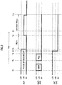
- the memory card 100 is provided with a memory section 150 made up of a non-volatile memory, a memory controller 151 that controls the memory section 150 and transmission/reception or the like of a transmission signal, an I/O cell 121 for inputting/outputting data and a connector 152 (including pin 1 to pin 9).
- the memory controller 151 is connected to the memory section 150 via a bus of, for example, 8-bit bus width.
- the connector 152 When the memory card 100 is attached to the host device 200, the connector 152 is electrically connected to the host device 200. Allocation of signal lines to the pin 1 to pin 9 included in the connector 152 is defined in the standard of an SD memory card (registered trademark).
- data DAT0, DAT1, DAT2 and DAT3 to transmit and receive a data signal are allocated to pin 7, pin 8, pin 9 and pin 1 respectively. Furthermore, the pin 1 is also allocated to a card detection signal CD.
- a command signal CMD and a response signal RES which is a response signal of the memory card 100 to this command signal are allocated to the pin 2.
- a clock signal CLK is allocated to the pin 5.
- a supply voltage VDD is allocated to the pin 4 and a grounding voltage VSS1 is allocated to the pin 3 and a grounding voltage VSS2 is allocated to the pin 6.
- the memory section 150 is a non-volatile semiconductor memory and made up of a NAND type flash memory. Data or the like sent from the host device 200 is stored in the memory section 150.
- the bus that transmits/receives a signal or the like between the memory card 100 and host device 200 includes a CLK line 111 (hereinafter also referred to as a "clock signal line”), a CMD/RES line 112 (hereinafter also referred to as a "CMD line”), a DAT[3:0] line 113 and a VDD line (hereinafter also referred to as a "power line”), and a DAT1 line, a DAT2 line, a CD/DAT3 line, a VSS1 line and a VSS2 line which are not shown.
- CLK line 111 hereinafter also referred to as a "clock signal line”
- CMD/RES line 112 hereinafter also referred to as a "CMD line”
- DAT[3:0] line 113 and a VDD line hereinafter also referred to as a "power line”
- the DAT0 line (hereinafter also referred to as a "data line”) will be explained as an example of the data signal line.
- the CMD/RES line is also referred to as a command signal line or response signal (RES) line. That is, the command signal line and the response signal line are one and the same signal line.
- an SD mode and an SPI mode are defined. Furthermore, as the transfer mode of the SD mode, two modes: a 1-bit mode using only the data DAT0 and a 4-bit mode using the data DAT0 to DAT3 are defined.
- a transfer mode of the memory card 100 in addition to a normal speed mode (NSM) of a normal transfer rate and a high-speed mode (HSM) of a speed doubling that of the NSM, an ultra-high-speed mode (UHSM) of a speed further doubling that of the HSP is defined depending on the transfer clock frequency or the like.
- NSM normal speed mode
- HSM high-speed mode
- UHSM ultra-high-speed mode
- the memory card 100 of the memory system 1 has a regulator (VR2) 116, which is a first regulator, and the host device 200 of the memory system 1 has a regulator (VR1) 204 which is a second regulator. Therefore, in addition to a data transfer mode whose signal voltage is a standard 3.3 V (hereinafter referred to as a "3.3 V mode") which is a voltage mode supported by many memory systems 1, the memory system 1 supports a mode in which the supply voltage remains standard 3.3 V and the data transfer signal voltage is set to a lower voltage 1.8 V (hereinafter referred to as a "1.8 V mode").
- 3.3 V mode a standard 3.3 V
- 1.8 V mode 1.8 V mode
- the memory card 100 has a multi-drive type first I/O cell 121 that can transmit and receive a command signal, response signal, clock signal and data signal to/from the host device 200 at any one signal voltage selected from a first voltage (3.3 V) and a second voltage (1.8 V), which is lower than the first voltage and the first regulator 116 that can output the first voltage and the second voltage, and the host device 200 has a multi-drive type second I/O cell 209 and the second regulator 204 of specifications similar to those of the memory card 100.
- a power switch (PSW) 201 is a switch that turns ON/OFF the supply voltage (VDD) applied to the memory card 100.
- Band gap references (BGR) 115 and 203 are reference voltage generation circuits using a potential difference of a band gap.
- Noise filters (Filter) 114 and 201 are not indispensable parts, yet effective in preventing noise from the power line (VDD) and generating more stable reference voltages.
- the first regulator (VR2) 116 and the second regulator (VR1) 204 are regulators that create a 1.8 V voltage from a 3.3 V supply voltage and generate the 1.8 V voltage based on the reference voltages of the BGRs 115 and 203 respectively.
- a third regulator (VR3) 122 which is a core voltage generation circuit, which is an internal logic circuit, generates a voltage supplied to a random logic section 123.
- the random logic section 123 is a circuit having the memory controller 151 shown in Fig. 1 , ROM and RAM or the like.
- the host device 200 may also need a voltage generation circuit for the internal logic, which is however not shown.
- a comparator (VDCLK) 120 which is a first voltage comparison circuit, detects whether or not the voltage of the CLK line is 1.8 V.
- a comparator (VDCMD/RES) 208 which is a second voltage comparison circuit, detects whether or not the voltage of the CMD/RES line is 1.8 V.
- a comparator 119 which is a third voltage comparison circuit or a comparator 207, which is a fourth voltage comparison circuit, detects whether or not a 1.8 V voltage is correctly generated from the first regulator (VR2) 116 or the second regulator (VR1) 204 respectively.
- the second voltage is 1.8 V means that the second voltage falls within a range of 1.65 V to 1.95 V.
- the comparator that detects whether a voltage is the first voltage or the second voltage is a voltage comparator having a third threshold voltage intermediate between the first voltage and the second voltage, decides on the first voltage when the voltage of the measurement line is higher than the third threshold voltage, and decides on the second voltage when the voltage of the measurement line is lower than the third threshold voltage.
- pull-up resistors 224 and 225 keep the voltage of each line to 3.3 V or 1.8 V. Furthermore, capacitors 118 and 206 accumulate charge to stabilize a predetermined voltage.
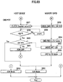
- Fig. 3A and Fig. 3B are flowcharts illustrating the signal voltage switching operation of the memory system 1 and Fig. 4 is a timing chart of a signal line group (bus) during the signal voltage switching operation of the memory system 1.
- the host device 200 performs a signal voltage switching operation taking into consideration compatibility with the memory card supporting only the 3.3 V mode. That is, if the host device 200 applies a 1.8 V signal voltage to the connected memory card from the beginning, the input I/O cell of the memory card supporting only the 3.3 V mode recognizes the applied 1.8 V as an intermediate voltage. Therefore, a large through current may flow through the input I/O cell of the memory card.
- the host device 200 follows a procedure of sending a signal of 3.3 V signal voltage to the memory card first and switching to the 1.8 V mode only after detecting that the memory card is a memory card that supports the 1.8 V mode through handshake processing which will be described later.
- Fig. 3A and Fig. 3B show the operation flow of the host device 200 and the right side shows the operation flow of the memory card 100.
- the memory card 100 is connected to the host device 200. That is, with the lines 111 to 113 making up the bus interface, the I/O cell 121 of the memory card 100 and the I/O cell 209 of the host device 200 are connected through the command /response signal line, clock signal line and data signal line or the like.
- the host device 200 inquires whether or not the connected memory card 100 supports the 1.8 V mode. That is, the host device 200 issues a command CMD8 first ( Fig. 4 : T1). Since a bit requesting the shift to the 1.8 V mode is set in an argument of the CMD8, the command signal CMD8 transmitted from this host device 200 to the memory card 100 is also a command signal that informs that the signal voltage will be changed from the first voltage (3.3 V) to the second voltage (1.8 V).
- the memory card 100 Upon receiving the command signal CMD8 from the host device, the memory card 100 decides whether or not the memory card 100 supports the 1.8 V mode.
- step S12 When the memory card 100 does not support the 1.8 V mode (step S12: No), the memory card 100 sends in reply a response signal indicating that the 1.8 V mode is not supported to the host device 200.
- step S12 when the memory card 100 supports the 1.8 V mode (step S12: Yes), the memory card 100 sends in reply a response signal indicating that the mode will be switched to the 1.8 V mode to the host device 200 ( Fig. 4 : T2).
- the host device 200 Upon receiving a response signal (No) indicating that the 1.8 V mode is not supported from the memory card 100, the host device 200 starts initialization processing in the 3.3 V mode in S33.
- the host device 200 upon receiving a response signal (Yes) indicating that the 1.8 V mode is supported from the memory card 100, the host device 200 performs processing of mutually sending a next transmission signal based on the contents of the received signal, so-called handshake processing.
- the host device 200 sets the DAT line to L level (ground level: 0 V) ( Fig. 4 : T4), stops clock oscillation and also sets the CLK line to L level (ground level: 0 V) ( Fig. 4 : T5). Any line of the DAT line and CLK line can be driven to L level first.
- the reason that the CMD line, CLK line and DAT line are set, that is, driven to L level (0 V) is to prevent the respective lines from becoming a tri-state and prevent unstable voltages from being applied.
- the host device 200 or memory card 100 fixes the voltage of the signal line to L level (0 V).
- the memory card 100 switches the regulator VR2 so as to generate 1.8 V. Furthermore, the host device 200 switches the regulator VR1 so as to generate 1.8 V.
- the host device 200 waits until a predetermined time elapses ( Fig. 4 : T5 to T6). Therefore, the timer sets 100 microseconds for example.
- the host device 200 needs to wait for the capacitors 206 and 118 connected to the regulator VR1 and regulator VR2 respectively to discharge from a state charged to 3.3 V to a state charged to 1.8 V.
- the memory system 1 is not provided with any discharge circuit.
- the waiting time is 100 microseconds, but the waiting time varies depending on the specification of the capacitor 206 or 118 and is generally on the order of 10 to 500 microseconds.
- the host device 200 sets the clock signal line at the ground level to 1.8 V for a predetermined time after a lapse of 100 microseconds in the above described example ( Fig. 4 : T6).
- the host device 200 applies a 1.8 V DC signal to the clock signal line which normally sends a clock signal.
- the host device 200 then informs the memory card 100 that the 1.8 V signal voltage can be supplied from the regulator VR2.
- the memory card 100 checks with the comparator 120, which is the first voltage comparison circuit, whether or not the signal voltage is 1.8 V. When no 1.8 V voltage is applied to the clock signal line (No), the memory card 100 does not perform further voltage switching processing and the memory card 100 stops operating in step S32.
- step S22 when the signal voltage of the clock signal line is confirmed to be 1.8 V (Yes), the memory card 100 drives the CMD/RES line (response signal line) at the ground level to 1.8 V ( Fig. 4 : T7).
- the memory card 100 applies a 1.8 V DC signal to the response signal line which normally sends a RES signal.
- the host device After setting the signal voltage of the clock signal line to 1.8 V, the host device sets the timer.
- VDCMD/RES the second voltage comparison circuit whether or not the signal voltage of the CMD/RES signal line is 1.8 V.
- the host device 200 turns OFF the power switch (PSW) 201 in step S27 and stops the operation of the memory card 100.
- the memory system 1 of the present embodiment may detect that switching to 1.8 V has not been successfully performed and thereby output an error code or execute initialization processing in a 3.3 V mode. An example thereof will be shown in Fig. 5 .
- Fig. 5 shows a timing chart when the memory card 100 has not driven the CMD/RES line (response signal line) to 1.8 V in step S23.
- the host device 200 applies a 1.8 V voltage to the clock signal line and waits for a response operation from the memory card 100, that is, for the response signal line to change from 0 V (ground level) to 1.8 V.
- the host device 200 turns OFF the power switch 201 at T12 and stops the supply voltage (VDD) applied to the memory card 100.
- VDD supply voltage
- the host device 200 sets the voltage of the CLK signal line to 0 V and stops the power supply to the memory card 100.
- step S24 when the signal voltage of the CMD/RES signal line is confirmed to be 1.8 V (Yes), the host device 200 sends an oscillating clock signal to the clock signal line, in other words, oscillates the clock signal ( Fig. 4 : T8).
- Step S29, step 30> Drive DAT to 1.8 V/DAT to tri-state
- the host device 200 drives the DAT signal line to a 1.8 V voltage for a short time ( Fig. 4 : T9 to T10), sets the DAT signal line to a tri-state. Since the DAT signal line is pulled up at 1.8 V, the voltage level of 1.8 V is maintained.
- step 32 > CLK oscillated?/CMD/RES to tri-state
- the memory card 100 Upon receiving the oscillating clock signal from the host device 200 (Yes), the memory card 100 sets the CMD/RES line to a tri-state in step S29 ( Fig. 4 : T11). Since the CMD/RES line is pulled up at 1.8 V, the 1.8 V voltage level is maintained.
- Both the memory card 100 and host device 200 perform initialization processing in the 3.3 V mode and transmits/receives subsequent signals at a 3.3 V signal voltage.
- Both the memory card 100 and host device 200 complete the processing of moving to the 1.8 V mode and transmits/receives subsequent signals at a 1.8 V signal voltage.
- the host device 200 turns OFF once the power and then sends the 3.3 V signal voltage to the memory card 100 again and performs initialization processing in the 3.3 V mode without switching to the 1.8 V mode.
- the memory card 100 and host device 200 mutually check signal voltages used through handshake processing and thereby prevent the I/O cell or the like from being damaged. Furthermore, in the memory system 1, the memory card 100 and host device 200 mutually check the voltage of the output of the regulator 116 or 204, and can thereby improve the reliability of the voltage applied to the signal line. Furthermore, the memory system 1 defines the handshake processing sequence using the clock signal line and command signal line, and can thereby follow a procedure to safely perform switching from the first voltage (3.3 V) to the second voltage (1.8 V).
- the memory system 1 can preferably perform normal processing of switching the signal voltage to the 1.8 V mode only at the first stage before the initialization processing starts. That is, after switching to the 1.8 V mode, the memory system 1 does not change the voltage mode even if a reset command is issued.
- the memory card 100 and host device 200 transmit and receive all signals at the second voltage of 1.8 V, and this state continues until the operation of the memory system 1 is completed where the supply voltage becomes 0 V.
- the memory system 1 Since the memory system 1 should not frequently switch the voltage mode, it is possible to maintain stability and reliability by preventing the signal voltage from being changed even by a reset
- Fig. 6 is a partial configuration diagram showing partial configurations of the I/O cells 121 and 209 of the memory card 100 and host device 200.
- Any one voltage of 3.3 V and 1.8 V which are the outputs of the regulators 204 and 116 is selected and applied to the I/O cells 209 and 121 of the host device 200 and memory card 100 respectively. Therefore, when the voltage is switched, there may be a time during which the output voltage of the regulator 204 differs from that of the regulator 116. When the output voltage of the regulator 204 is different from that of the regulator 116, a current may flow through an unexpected path and damage the I/O cell 121 or 209 or the like.
- protection diodes 232 and 136 are connected to the power lines of a 3.3 V voltage. Therefore, in the host device 200 and memory card 100, a protection diode 137 or 233 is not damaged by an applied voltage exceeding 1.8 V even in the 1.8 V mode.
- the memory card 100 has the non-volatile memory section 150 which is connectable to the host device 200, the power line VDD 114 that supplies the first voltage (3.3 V), the first regulator 116 that can output power of any one voltage selected from the first voltage (3.3 V) and the second voltage (1.8 V) which is lower than the first voltage from the VDD 114, the I/O cell 121 that receives the power supply from the first regulator 116 and transmits/receives signals to/from the host device 200, and the protection diode 136 connected to an input end of the I/O cell 121 and an end of the power supply connected to the 3.3 V power line to protect the I/O cell 121 from an overvoltage, wherein it is possible to perform transmission/reception to/from the host device 200 with a signal of any one voltage selected from the first voltage (3.3 V) and second voltage (1.8 V).
- both the host device 200 and memory card 100 have the regulator 116 or 204 that can output two voltages, and therefore connecting the protection diode to the regulator output may damage the protection diode.
- the signal voltage is set to 1.8 V
- the supply voltage itself is generally set to 1.8 V, but since compatibility is taken into consideration in the memory system 1, the supply voltage is set to 3.3 V. Therefore, the above described protection diode 136 is effective in preventing damage to the protection diode in the memory system 1.
- Fig. 7A and Fig. 7B are diagrams illustrating parameter examples of a switch command for changing the transfer mode in which the host device 200 performs transmission.
- the present embodiment has explained the memory system 1 or the like having an SD memory card (registered trademark) as the memory device for an example, but the present embodiment is also applicable to a memory system having another memory card, memory device, inner memory or the like as long as the memory system has a similar bus structure and can exert operations and effects similar to those of the memory system 1 or the like.
- SD memory card registered trademark
- the present embodiment is also applicable to a memory system having another memory card, memory device, inner memory or the like as long as the memory system has a similar bus structure and can exert operations and effects similar to those of the memory system 1 or the like.
- the memory device or the like of the present invention is as follows.
- the memory device or the like of the present invention is a memory system having the memory device according to 2 to 8 above, a method of controlling the memory device and a method of controlling the memory system according to 2 to 8 above.
- a memory system 301 having a memory card 400 which is a memory device, a host device 500, a memory card 400 and a host device 500 according to a second embodiment of the present invention will be explained with reference to the accompanying drawings. Since the memory system 301 or the like of the present embodiment is similar to the memory system 1 or the like according to the first embodiment, the same components will be assigned the same reference numerals and explanations thereof will be omitted.
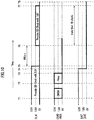
- Fig. 8A and Fig. 8B are flowcharts illustrating the signal voltage switching operation of the memory system 301 and Fig. 9 and Fig. 10 are timing charts of a signal line group (bus) during the signal voltage switching operation of the memory system 301.
- Fig. 8A and Fig. 8B show an operation flow of the host device 500 and the right side shows an operation flow of the memory card 400.
- step S10 to step S 14 of the memory system 1 or the like, explanations thereof will be omitted.
- Step S45> Drive CMD/RES to 0 V, drive DAT to 0 V
- the host device 500 stops clock oscillation and also sets the CLK line to L level (ground level: 0 V) ( Fig. 9 : T5).
- step S 17 to step S20 of the memory system 1 or the like Since these steps are the same as step S 17 to step S20 of the memory system 1 or the like, explanations thereof will be omitted.
- the host device 500 After a lapse of a predetermined period (e.g., 100 microseconds) in the steps 49,50, the host device 500 sends an oscillating clock signal to a clock signal line, in other words, oscillates a clock signal ( Fig. 9 : T6). The host device 500 then informs the memory card 400 that a 1.8 V signal voltage can be supplied from a regulator VR2.
- a predetermined period e.g. 100 microseconds
- the memory card 400 checks whether or not an H level clock signal of a predetermined voltage is applied to the clock signal line.
- This step is the same as step S23 of the memory system 1 or the like and therefore explanations thereof will be omitted.
- the memory card 400 drives the CMD/RES line to a 1.8 V voltage for only a short time ( Fig. 9 : T7 to T8), and then sets the CMD/RES line to a tri-state ( Fig. 9 : T8). Since the CMD/RES line is pulled up at 1.8 V, the voltage level of 1.8 V is maintained.
- Step S55 step 56> Drive DAT to 1.8 V/DAT to tri-state
- the memory card 400 drives the DAT signal line to a 1.8 V mode voltage for only a short time ( Fig. 9 : T9 to T10), then sets the DAT signal line to a tri-state. Since the DAT signal line is pulled up at 1.8 V, the voltage level of 1.8 V is maintained.
- the host device 500 sets the clock counter after oscillating the clock signal and then sets a count n to 0.
- the host device 500 waits until at least 16 clocks are counted. A value equal to or greater than 16 clocks is set as the waiting time.
- the host device 500 detects that the DAT signal line is not at a ground level, that is, that a predetermined voltage is applied.
- the predetermined voltage is 1.8 V.
- the host device 500 When no voltage is applied to the DAT signal line (No), the host device 500 turns OFF a power switch (PSW) 201 in step S61 and stops operation of the memory card 400.
- PSW power switch
- step S63 the host device 500 transmits/receives subsequent signals at a 1.8 V signal voltage.
- the host device 500 detects that not only the DAT signal line but also the DAT signal line and CMD signal line are not at a ground level, that is, by detecting that a predetermined voltage is applied, it is possible to perform voltage switching processing more safely.
- the predetermined voltage is 1.8 V.
- Both the memory card 400 and the host device 500 perform initialization processing in a 3.3 V mode and transmits/receives subsequent signals at a 3.3 V signal voltage.
- Both the memory card 400 and the host device 500 complete the processing of moving to the 1.8 V mode and transmits/receives subsequent signals at a 1.8 V signal voltage.
- the host device 500 turns OFF once the power, sends a 3.3 V signal voltage to the memory card 400 again and performs initialization processing in the 3.3 V mode without switching to the 1.8 V mode.
- the memory card 400 of the memory system 301 detects the voltage of the oscillation clock signal outputted by the host device 500. This eliminates the necessity for a circuit that applies a DC voltage to the clock signal line, which is required in the memory system 1. Furthermore, the memory card 400 sets the DAT line to a tri-state.
- the memory system 301 of the present embodiment can still exert effects similar to those of the memory system 1 of the first embodiment.
- a memory card 700 which is a memory device, a host device 800 and a memory system 601 having the memory card 700 and the host device 800 according to a third embodiment of the present invention will be explained.
- the memory system 601 or the like of the present embodiment is similar to the memory system 301 or the like of the second embodiment, and therefore the same components will be assigned the same reference numerals and explanations thereof will be omitted.
- the memory system 601 or the like is not provided with the comparators 119, 120, 207, 208 (see Fig. 2 ) for confirming that the voltage is a desired voltage, for example, 1.8 V.
- the memory card 700 checks in step S52 in Fig. 8A that the clock signal line is not at a ground level, that is, only the presence/absence of clock oscillation. Furthermore, in step S55 in Fig. 8B , the host device 800 only checks whether or not any voltage is applied to the CMD line, that is, whether or not the CMD line is at a ground level.
- the memory system 601 of the present embodiment can still exert effects similar to those of the memory system 1 or the like of the first embodiment.
Landscapes
- Engineering & Computer Science (AREA)
- Theoretical Computer Science (AREA)
- Computer Hardware Design (AREA)
- Physics & Mathematics (AREA)
- General Physics & Mathematics (AREA)
- General Engineering & Computer Science (AREA)
- Microelectronics & Electronic Packaging (AREA)
- Power Sources (AREA)
- Read Only Memory (AREA)
- Techniques For Improving Reliability Of Storages (AREA)
Applications Claiming Priority (4)
| Application Number | Priority Date | Filing Date | Title |
|---|---|---|---|
| JP2008072429 | 2008-03-19 | ||
| JP2008099740A JP5106219B2 (ja) | 2008-03-19 | 2008-04-07 | メモリデバイス、ホストデバイス、メモリシステム、メモリデバイスの制御方法、ホストデバイスの制御方法、およびメモリシステムの制御方法 |
| PCT/JP2008/066618 WO2009116196A1 (en) | 2008-03-19 | 2008-09-09 | Memory device, host device, memory system5 memory device control method, host device control method and memory system control method |
| EP08873506.3A EP2266042B8 (de) | 2008-03-19 | 2008-09-09 | Speichereinrichtung, hosteinrichtung, speichersystem, speichereinrichtungs-steuerverfahren, hosteinrichtungs-steuerverfahren und speichersystem-steuerverfahren |
Related Parent Applications (2)
| Application Number | Title | Priority Date | Filing Date |
|---|---|---|---|
| EP08873506.3A Division EP2266042B8 (de) | 2008-03-19 | 2008-09-09 | Speichereinrichtung, hosteinrichtung, speichersystem, speichereinrichtungs-steuerverfahren, hosteinrichtungs-steuerverfahren und speichersystem-steuerverfahren |
| EP08873506.3A Division-Into EP2266042B8 (de) | 2008-03-19 | 2008-09-09 | Speichereinrichtung, hosteinrichtung, speichersystem, speichereinrichtungs-steuerverfahren, hosteinrichtungs-steuerverfahren und speichersystem-steuerverfahren |
Publications (2)
| Publication Number | Publication Date |
|---|---|
| EP3343381A1 true EP3343381A1 (de) | 2018-07-04 |
| EP3343381B1 EP3343381B1 (de) | 2020-10-21 |
Family
ID=41090614
Family Applications (2)
| Application Number | Title | Priority Date | Filing Date |
|---|---|---|---|
| EP08873506.3A Active EP2266042B8 (de) | 2008-03-19 | 2008-09-09 | Speichereinrichtung, hosteinrichtung, speichersystem, speichereinrichtungs-steuerverfahren, hosteinrichtungs-steuerverfahren und speichersystem-steuerverfahren |
| EP18151595.8A Active EP3343381B1 (de) | 2008-03-19 | 2008-09-09 | Speichervorrichtung, hostvorrichtung, speichersystem, speichervorrichtungsteuerungsverfahren, hostvorrichtungsteuerungsverfahren und speichersystemsteuerungsverfahren |
Family Applications Before (1)
| Application Number | Title | Priority Date | Filing Date |
|---|---|---|---|
| EP08873506.3A Active EP2266042B8 (de) | 2008-03-19 | 2008-09-09 | Speichereinrichtung, hosteinrichtung, speichersystem, speichereinrichtungs-steuerverfahren, hosteinrichtungs-steuerverfahren und speichersystem-steuerverfahren |
Country Status (7)
| Country | Link |
|---|---|
| US (7) | US8321697B2 (de) |
| EP (2) | EP2266042B8 (de) |
| JP (1) | JP5106219B2 (de) |
| KR (1) | KR101269347B1 (de) |
| CN (2) | CN101978360B (de) |
| TW (1) | TWI414944B (de) |
| WO (1) | WO2009116196A1 (de) |
Families Citing this family (39)
| Publication number | Priority date | Publication date | Assignee | Title |
|---|---|---|---|---|
| JP5106219B2 (ja) * | 2008-03-19 | 2012-12-26 | 株式会社東芝 | メモリデバイス、ホストデバイス、メモリシステム、メモリデバイスの制御方法、ホストデバイスの制御方法、およびメモリシステムの制御方法 |
| US8924661B1 (en) | 2009-01-18 | 2014-12-30 | Apple Inc. | Memory system including a controller and processors associated with memory devices |
| EP2315401B1 (de) * | 2009-03-24 | 2016-11-30 | B&Plus K.K. | Ein-/ausgangssignalsteuergerät und ein-/ausgangssignalsteuersystem |
| US8977805B2 (en) * | 2009-03-25 | 2015-03-10 | Apple Inc. | Host-assisted compaction of memory blocks |
| US8832354B2 (en) | 2009-03-25 | 2014-09-09 | Apple Inc. | Use of host system resources by memory controller |
| US8489837B1 (en) | 2009-06-12 | 2013-07-16 | Netlist, Inc. | Systems and methods for handshaking with a memory module |
| JP5789759B2 (ja) * | 2010-03-16 | 2015-10-07 | パナソニックIpマネジメント株式会社 | 情報処理装置、不揮発性記憶装置、情報処理システム及び不揮発性メモリコントローラ |
| JP2012168865A (ja) * | 2011-02-16 | 2012-09-06 | Toshiba Corp | メモリシステム |
| TW201322136A (zh) * | 2011-10-13 | 2013-06-01 | 松下電器產業股份有限公司 | 鄰近非接觸通訊裝置、系統及方法 |
| US9329990B2 (en) * | 2013-01-11 | 2016-05-03 | Micron Technology, Inc. | Host controlled enablement of automatic background operations in a memory device |
| US9383794B2 (en) * | 2014-06-11 | 2016-07-05 | Freescale Semiconductor, Inc. | Integrated circuit with multi-voltage input/output (I/O) cells |
| KR102285789B1 (ko) * | 2014-07-01 | 2021-08-04 | 삼성전자 주식회사 | 외장 저장 장치, 및 이의 기준 주파수를 설정하는 방법 |
| JP2016029556A (ja) * | 2014-07-15 | 2016-03-03 | 株式会社東芝 | ホスト機器および拡張性デバイス |
| US9639291B2 (en) | 2014-09-10 | 2017-05-02 | Kabushiki Kaisha Toshiba | Memory system |
| US9886080B2 (en) * | 2014-12-30 | 2018-02-06 | Sandisk Technologies Llc | Low voltage detection and initialization for non-volatile memory systems |
| WO2016132733A1 (ja) * | 2015-02-16 | 2016-08-25 | パナソニックIpマネジメント株式会社 | ホスト装置、スレーブ装置、インターフェイス半導体装置及びリムーバブルシステム |
| KR102291806B1 (ko) * | 2015-04-20 | 2021-08-24 | 삼성전자주식회사 | 불휘발성 메모리 시스템 및 그것의 동작 방법 |
| JP2017097825A (ja) * | 2015-11-16 | 2017-06-01 | 株式会社東芝 | ホスト機器および拡張デバイス |
| JP6620313B2 (ja) * | 2016-01-06 | 2019-12-18 | パナソニックIpマネジメント株式会社 | ホスト装置、スレーブ装置及びリムーバブルシステム |
| US9898218B2 (en) * | 2016-02-05 | 2018-02-20 | International Business Machines Corporation | Memory system with switchable operating bands |
| CN105892609B (zh) * | 2016-04-06 | 2019-06-04 | 惠州Tcl移动通信有限公司 | 一种终端开机与识别存储卡同步运行的方法及智能终端 |
| US10242719B2 (en) * | 2016-04-08 | 2019-03-26 | Samsung Electronics Co., Ltd. | Power management of a memory device by dynamically changing supply voltage |
| US10019306B2 (en) * | 2016-04-27 | 2018-07-10 | Western Digital Technologies, Inc. | Collision detection for slave storage devices |
| KR20180006164A (ko) * | 2016-07-08 | 2018-01-17 | 에스케이하이닉스 주식회사 | 메모리 시스템 및 메모리 시스템의 동작 방법 |
| US10061378B2 (en) * | 2016-07-29 | 2018-08-28 | Sandisk Technologies Llc | System and method for adjusting device performance based on sensed host current sourcing capability |
| KR102758703B1 (ko) * | 2016-10-07 | 2025-01-22 | 삼성전자주식회사 | 하위 호환성을 유지하는 메모리 시스템 및 호스트 장치 |
| KR102660729B1 (ko) * | 2016-10-28 | 2024-04-26 | 삼성전자주식회사 | 전원 잡음을 검출하는 불휘발성 메모리 장치 및 그것의 동작 방법 |
| US11003237B2 (en) * | 2018-04-12 | 2021-05-11 | Silicon Motion, Inc. | Method for performing power management in a memory device, associated memory device and controller thereof, and associated electronic device |
| TWI722521B (zh) * | 2019-08-02 | 2021-03-21 | 新唐科技股份有限公司 | 控制裝置及調整方法 |
| JP7493369B2 (ja) | 2020-03-30 | 2024-05-31 | キヤノン株式会社 | 通信装置、制御方法、及びプログラム |
| JP7494071B2 (ja) * | 2020-09-23 | 2024-06-03 | キオクシア株式会社 | メモリシステム |
| EP4254211A4 (de) * | 2020-11-24 | 2024-05-01 | Panasonic Intellectual Property Management Co., Ltd. | Host-vorrichtung, slave-vorrichtung und datenübertragungssystem |
| WO2023277865A1 (en) * | 2021-06-28 | 2023-01-05 | Hewlett-Packard Development Company, L.P. | Identification of option cards using multiple voltage inputs |
| CN115620762B (zh) * | 2021-07-16 | 2026-02-17 | 瑞昱半导体股份有限公司 | 存储器系统及其存储器存取界面装置 |
| US12468334B2 (en) * | 2021-07-27 | 2025-11-11 | Synopsys, Inc. | Clock signal realignment for emulation of a circuit design |
| TWI789147B (zh) * | 2021-12-07 | 2023-01-01 | 瑞昱半導體股份有限公司 | 讀卡裝置及具有讀卡功能的電子裝置 |
| WO2023162555A1 (ja) * | 2022-02-22 | 2023-08-31 | パナソニックIpマネジメント株式会社 | ホスト装置、スレーブ装置およびホスト-スレーブシステム |
| JP2023141299A (ja) * | 2022-03-23 | 2023-10-05 | キオクシア株式会社 | メモリシステム |
| JP7559159B1 (ja) | 2023-08-01 | 2024-10-01 | レノボ・シンガポール・プライベート・リミテッド | 情報処理装置 |
Citations (4)
| Publication number | Priority date | Publication date | Assignee | Title |
|---|---|---|---|---|
| EP1551031A2 (de) * | 2003-12-31 | 2005-07-06 | Samsung Electronics Co., Ltd. | Halbleiterbauelement-Karte |
| JP2007011788A (ja) | 2005-06-30 | 2007-01-18 | Toshiba Corp | メモリカード及びそのホスト機器 |
| JP2008072429A (ja) | 2006-09-14 | 2008-03-27 | Toshiba Corp | トライステートバッファ回路 |
| JP2008099740A (ja) | 2006-10-17 | 2008-05-01 | Toshiba Corp | 乳房断層撮影装置、画像表示方法及びプログラム |
Family Cites Families (26)
| Publication number | Priority date | Publication date | Assignee | Title |
|---|---|---|---|---|
| US5190117A (en) * | 1990-07-11 | 1993-03-02 | Pitney Bowes Inc. | Load cell supporting member and weighing scale incorporating the same |
| JP3477781B2 (ja) * | 1993-03-23 | 2003-12-10 | セイコーエプソン株式会社 | Icカード |
| JPH09231339A (ja) | 1996-02-27 | 1997-09-05 | Mitsubishi Electric Corp | メモリカード |
| JP2001134356A (ja) * | 1999-11-05 | 2001-05-18 | Toshiba Tec Corp | 信号伝送制御装置 |
| JP4649009B2 (ja) * | 2000-03-08 | 2011-03-09 | 株式会社東芝 | カードインタフェースを備えた情報処理装置、同装置に装着可能なカード型電子機器、及び同装置におけ動作モード設定方法 |
| JP3461323B2 (ja) * | 2000-03-28 | 2003-10-27 | シャープ株式会社 | Pcカード |
| US6434044B1 (en) * | 2001-02-16 | 2002-08-13 | Sandisk Corporation | Method and system for generation and distribution of supply voltages in memory systems |
| CN1299234C (zh) * | 2001-06-04 | 2007-02-07 | 株式会社瑞萨科技 | 存储卡 |
| KR100466981B1 (ko) | 2002-03-04 | 2005-01-24 | 삼성전자주식회사 | 저전압 불휘발성 반도체 메모리 장치 |
| US7417335B2 (en) * | 2002-07-22 | 2008-08-26 | Seagate Technology Llc | Method and apparatus for integrated circuit power up |
| JP2004333103A (ja) | 2003-03-12 | 2004-11-25 | Hanagami Tekkosho:Kk | 冷却式加熱バーナー |
| JP4653960B2 (ja) * | 2003-08-07 | 2011-03-16 | ルネサスエレクトロニクス株式会社 | メモリカードおよび不揮発性メモリ混載マイコン |
| KR100560767B1 (ko) * | 2003-09-02 | 2006-03-13 | 삼성전자주식회사 | 탈착 가능한 저장 장치를 포함하는 시스템 및 그것의 제어방법 |
| JP4723381B2 (ja) * | 2004-01-06 | 2011-07-13 | dブロード株式会社 | バスシェアーアダプター機能を有するsdioカードデバイス |
| US20050268124A1 (en) * | 2004-05-25 | 2005-12-01 | Hewlett-Packard Development Company, L.P. | Apparatus and method for voltage switching |
| WO2006057049A1 (ja) | 2004-11-26 | 2006-06-01 | Kabushiki Kaisha Toshiba | カードおよびホスト機器 |
| KR101107152B1 (ko) * | 2004-12-16 | 2012-02-06 | 삼성전자주식회사 | 동작 성능이 향상된 메모리 저장 장치 |
| WO2006117966A1 (ja) * | 2005-04-27 | 2006-11-09 | Matsushita Electric Industrial Co., Ltd. | カード型電子装置及びホスト装置 |
| TW200639873A (en) * | 2005-05-06 | 2006-11-16 | Silicon Power Comp & Comm Inc | System for converting input voltage in memory card |
| US8175717B2 (en) | 2005-09-06 | 2012-05-08 | Boston Scientific Neuromodulation Corporation | Ultracapacitor powered implantable pulse generator with dedicated power supply |
| US7373533B2 (en) * | 2005-09-30 | 2008-05-13 | Silicon Laboratories | Programmable I/O cell capable of holding its state in power-down mode |
| CN101060007B (zh) * | 2006-04-17 | 2010-10-06 | 科统科技股份有限公司 | 复合存储器芯片 |
| JP5226669B2 (ja) | 2006-04-24 | 2013-07-03 | サンディスク テクノロジィース インコーポレイテッド | 高効率フラッシュメモリデータ転送 |
| JP2009176136A (ja) | 2008-01-25 | 2009-08-06 | Toshiba Corp | 半導体記憶装置 |
| JP5106219B2 (ja) * | 2008-03-19 | 2012-12-26 | 株式会社東芝 | メモリデバイス、ホストデバイス、メモリシステム、メモリデバイスの制御方法、ホストデバイスの制御方法、およびメモリシステムの制御方法 |
| JP6333103B2 (ja) | 2013-11-20 | 2018-05-30 | キヤノン株式会社 | 画像形成装置 |
-
2008
- 2008-04-07 JP JP2008099740A patent/JP5106219B2/ja active Active
- 2008-09-09 CN CN200880128158XA patent/CN101978360B/zh active Active
- 2008-09-09 US US12/933,586 patent/US8321697B2/en not_active Expired - Fee Related
- 2008-09-09 KR KR1020107020950A patent/KR101269347B1/ko active Active
- 2008-09-09 CN CN201310205495.7A patent/CN103366211B/zh active Active
- 2008-09-09 EP EP08873506.3A patent/EP2266042B8/de active Active
- 2008-09-09 EP EP18151595.8A patent/EP3343381B1/de active Active
- 2008-09-09 WO PCT/JP2008/066618 patent/WO2009116196A1/en not_active Ceased
- 2008-10-17 TW TW097140047A patent/TWI414944B/zh active
-
2012
- 2012-11-02 US US13/667,285 patent/US8799689B2/en active Active
-
2014
- 2014-06-23 US US14/312,543 patent/US9383792B2/en not_active Ceased
-
2017
- 2017-03-20 US US15/463,738 patent/USRE47308E1/en active Active
-
2019
- 2019-01-16 US US16/249,093 patent/USRE48418E1/en active Active
-
2020
- 2020-12-28 US US17/135,608 patent/USRE49235E1/en active Active
-
2022
- 2022-08-18 US US17/890,773 patent/USRE49829E1/en active Active
Patent Citations (4)
| Publication number | Priority date | Publication date | Assignee | Title |
|---|---|---|---|---|
| EP1551031A2 (de) * | 2003-12-31 | 2005-07-06 | Samsung Electronics Co., Ltd. | Halbleiterbauelement-Karte |
| JP2007011788A (ja) | 2005-06-30 | 2007-01-18 | Toshiba Corp | メモリカード及びそのホスト機器 |
| JP2008072429A (ja) | 2006-09-14 | 2008-03-27 | Toshiba Corp | トライステートバッファ回路 |
| JP2008099740A (ja) | 2006-10-17 | 2008-05-01 | Toshiba Corp | 乳房断層撮影装置、画像表示方法及びプログラム |
Also Published As
| Publication number | Publication date |
|---|---|
| EP3343381B1 (de) | 2020-10-21 |
| USRE49235E1 (en) | 2022-10-04 |
| US20130060995A1 (en) | 2013-03-07 |
| CN103366211A (zh) | 2013-10-23 |
| CN103366211B (zh) | 2016-07-06 |
| EP2266042A4 (de) | 2016-08-03 |
| US20140304533A1 (en) | 2014-10-09 |
| USRE47308E1 (en) | 2019-03-19 |
| USRE49829E1 (en) | 2024-02-06 |
| US8321697B2 (en) | 2012-11-27 |
| US20110022789A1 (en) | 2011-01-27 |
| JP5106219B2 (ja) | 2012-12-26 |
| KR20100114937A (ko) | 2010-10-26 |
| JP2009258773A (ja) | 2009-11-05 |
| WO2009116196A1 (en) | 2009-09-24 |
| USRE48418E1 (en) | 2021-02-02 |
| US9383792B2 (en) | 2016-07-05 |
| KR101269347B1 (ko) | 2013-05-31 |
| EP2266042A1 (de) | 2010-12-29 |
| CN101978360A (zh) | 2011-02-16 |
| TWI414944B (zh) | 2013-11-11 |
| EP2266042B8 (de) | 2018-06-06 |
| TW200941227A (en) | 2009-10-01 |
| US8799689B2 (en) | 2014-08-05 |
| EP2266042B1 (de) | 2018-01-17 |
| CN101978360B (zh) | 2013-07-03 |
Similar Documents
| Publication | Publication Date | Title |
|---|---|---|
| EP2266042B1 (de) | Speichereinrichtung, hosteinrichtung, speichersystem, speichereinrichtungs-steuerverfahren, hosteinrichtungs-steuerverfahren und speichersystem-steuerverfahren | |
| US20230106495A1 (en) | Memory card and host device thereof | |
| KR100507252B1 (ko) | 파워-온 리세트 회로 및 ic 장치 | |
| JP4565883B2 (ja) | 半導体集積回路装置 | |
| KR100495657B1 (ko) | 복수의 통신 모드들을 갖는 집적 회로 장치 및 그것의동작 방법 | |
| US7875996B2 (en) | Multi-regulator power delivery system for ASIC cores | |
| US10339083B2 (en) | Host device, slave device, and removable system | |
| US20090160256A1 (en) | Multi-regulator power delivery system for ASIC cores | |
| US12314107B2 (en) | Method, circuit and apparatus for protecting power supply of PCIE card, and medium | |
| EP2223420B1 (de) | Multiregler-stromversorgungssystem für asic-kerne | |
| JP3904860B2 (ja) | 電源装置、半導体回路装置、およびicカード |
Legal Events
| Date | Code | Title | Description |
|---|---|---|---|
| PUAI | Public reference made under article 153(3) epc to a published international application that has entered the european phase |
Free format text: ORIGINAL CODE: 0009012 |
|
| STAA | Information on the status of an ep patent application or granted ep patent |
Free format text: STATUS: REQUEST FOR EXAMINATION WAS MADE |
|
| 17P | Request for examination filed |
Effective date: 20180115 |
|
| AC | Divisional application: reference to earlier application |
Ref document number: 2266042 Country of ref document: EP Kind code of ref document: P |
|
| AK | Designated contracting states |
Kind code of ref document: A1 Designated state(s): AT BE BG CH CY CZ DE DK EE ES FI FR GB GR HR HU IE IS IT LI LT LU LV MC MT NL NO PL PT RO SE SI SK TR |
|
| STAA | Information on the status of an ep patent application or granted ep patent |
Free format text: STATUS: EXAMINATION IS IN PROGRESS |
|
| 17Q | First examination report despatched |
Effective date: 20191216 |
|
| GRAP | Despatch of communication of intention to grant a patent |
Free format text: ORIGINAL CODE: EPIDOSNIGR1 |
|
| STAA | Information on the status of an ep patent application or granted ep patent |
Free format text: STATUS: GRANT OF PATENT IS INTENDED |
|
| INTG | Intention to grant announced |
Effective date: 20200420 |
|
| GRAS | Grant fee paid |
Free format text: ORIGINAL CODE: EPIDOSNIGR3 |
|
| GRAA | (expected) grant |
Free format text: ORIGINAL CODE: 0009210 |
|
| STAA | Information on the status of an ep patent application or granted ep patent |
Free format text: STATUS: THE PATENT HAS BEEN GRANTED |
|
| AC | Divisional application: reference to earlier application |
Ref document number: 2266042 Country of ref document: EP Kind code of ref document: P |
|
| AK | Designated contracting states |
Kind code of ref document: B1 Designated state(s): AT BE BG CH CY CZ DE DK EE ES FI FR GB GR HR HU IE IS IT LI LT LU LV MC MT NL NO PL PT RO SE SI SK TR |
|
| REG | Reference to a national code |
Ref country code: GB Ref legal event code: FG4D |
|
| REG | Reference to a national code |
Ref country code: CH Ref legal event code: EP |
|
| REG | Reference to a national code |
Ref country code: IE Ref legal event code: FG4D |
|
| REG | Reference to a national code |
Ref country code: DE Ref legal event code: R096 Ref document number: 602008063400 Country of ref document: DE |
|
| REG | Reference to a national code |
Ref country code: AT Ref legal event code: REF Ref document number: 1326534 Country of ref document: AT Kind code of ref document: T Effective date: 20201115 |
|
| REG | Reference to a national code |
Ref country code: AT Ref legal event code: MK05 Ref document number: 1326534 Country of ref document: AT Kind code of ref document: T Effective date: 20201021 |
|
| REG | Reference to a national code |
Ref country code: NL Ref legal event code: MP Effective date: 20201021 |
|
| PG25 | Lapsed in a contracting state [announced via postgrant information from national office to epo] |
Ref country code: FI Free format text: LAPSE BECAUSE OF FAILURE TO SUBMIT A TRANSLATION OF THE DESCRIPTION OR TO PAY THE FEE WITHIN THE PRESCRIBED TIME-LIMIT Effective date: 20201021 Ref country code: PT Free format text: LAPSE BECAUSE OF FAILURE TO SUBMIT A TRANSLATION OF THE DESCRIPTION OR TO PAY THE FEE WITHIN THE PRESCRIBED TIME-LIMIT Effective date: 20210222 Ref country code: NO Free format text: LAPSE BECAUSE OF FAILURE TO SUBMIT A TRANSLATION OF THE DESCRIPTION OR TO PAY THE FEE WITHIN THE PRESCRIBED TIME-LIMIT Effective date: 20210121 Ref country code: GR Free format text: LAPSE BECAUSE OF FAILURE TO SUBMIT A TRANSLATION OF THE DESCRIPTION OR TO PAY THE FEE WITHIN THE PRESCRIBED TIME-LIMIT Effective date: 20210122 |
|
| REG | Reference to a national code |
Ref country code: LT Ref legal event code: MG4D |
|
| PG25 | Lapsed in a contracting state [announced via postgrant information from national office to epo] |
Ref country code: AT Free format text: LAPSE BECAUSE OF FAILURE TO SUBMIT A TRANSLATION OF THE DESCRIPTION OR TO PAY THE FEE WITHIN THE PRESCRIBED TIME-LIMIT Effective date: 20201021 Ref country code: ES Free format text: LAPSE BECAUSE OF FAILURE TO SUBMIT A TRANSLATION OF THE DESCRIPTION OR TO PAY THE FEE WITHIN THE PRESCRIBED TIME-LIMIT Effective date: 20201021 Ref country code: BG Free format text: LAPSE BECAUSE OF FAILURE TO SUBMIT A TRANSLATION OF THE DESCRIPTION OR TO PAY THE FEE WITHIN THE PRESCRIBED TIME-LIMIT Effective date: 20210121 Ref country code: IS Free format text: LAPSE BECAUSE OF FAILURE TO SUBMIT A TRANSLATION OF THE DESCRIPTION OR TO PAY THE FEE WITHIN THE PRESCRIBED TIME-LIMIT Effective date: 20210221 Ref country code: LV Free format text: LAPSE BECAUSE OF FAILURE TO SUBMIT A TRANSLATION OF THE DESCRIPTION OR TO PAY THE FEE WITHIN THE PRESCRIBED TIME-LIMIT Effective date: 20201021 Ref country code: PL Free format text: LAPSE BECAUSE OF FAILURE TO SUBMIT A TRANSLATION OF THE DESCRIPTION OR TO PAY THE FEE WITHIN THE PRESCRIBED TIME-LIMIT Effective date: 20201021 Ref country code: SE Free format text: LAPSE BECAUSE OF FAILURE TO SUBMIT A TRANSLATION OF THE DESCRIPTION OR TO PAY THE FEE WITHIN THE PRESCRIBED TIME-LIMIT Effective date: 20201021 |
|
| PG25 | Lapsed in a contracting state [announced via postgrant information from national office to epo] |
Ref country code: NL Free format text: LAPSE BECAUSE OF FAILURE TO SUBMIT A TRANSLATION OF THE DESCRIPTION OR TO PAY THE FEE WITHIN THE PRESCRIBED TIME-LIMIT Effective date: 20201021 Ref country code: HR Free format text: LAPSE BECAUSE OF FAILURE TO SUBMIT A TRANSLATION OF THE DESCRIPTION OR TO PAY THE FEE WITHIN THE PRESCRIBED TIME-LIMIT Effective date: 20201021 |
|
| REG | Reference to a national code |
Ref country code: DE Ref legal event code: R097 Ref document number: 602008063400 Country of ref document: DE |
|
| PG25 | Lapsed in a contracting state [announced via postgrant information from national office to epo] |
Ref country code: LT Free format text: LAPSE BECAUSE OF FAILURE TO SUBMIT A TRANSLATION OF THE DESCRIPTION OR TO PAY THE FEE WITHIN THE PRESCRIBED TIME-LIMIT Effective date: 20201021 Ref country code: EE Free format text: LAPSE BECAUSE OF FAILURE TO SUBMIT A TRANSLATION OF THE DESCRIPTION OR TO PAY THE FEE WITHIN THE PRESCRIBED TIME-LIMIT Effective date: 20201021 Ref country code: CZ Free format text: LAPSE BECAUSE OF FAILURE TO SUBMIT A TRANSLATION OF THE DESCRIPTION OR TO PAY THE FEE WITHIN THE PRESCRIBED TIME-LIMIT Effective date: 20201021 Ref country code: SK Free format text: LAPSE BECAUSE OF FAILURE TO SUBMIT A TRANSLATION OF THE DESCRIPTION OR TO PAY THE FEE WITHIN THE PRESCRIBED TIME-LIMIT Effective date: 20201021 Ref country code: RO Free format text: LAPSE BECAUSE OF FAILURE TO SUBMIT A TRANSLATION OF THE DESCRIPTION OR TO PAY THE FEE WITHIN THE PRESCRIBED TIME-LIMIT Effective date: 20201021 |
|
| PLBE | No opposition filed within time limit |
Free format text: ORIGINAL CODE: 0009261 |
|
| STAA | Information on the status of an ep patent application or granted ep patent |
Free format text: STATUS: NO OPPOSITION FILED WITHIN TIME LIMIT |
|
| PG25 | Lapsed in a contracting state [announced via postgrant information from national office to epo] |
Ref country code: DK Free format text: LAPSE BECAUSE OF FAILURE TO SUBMIT A TRANSLATION OF THE DESCRIPTION OR TO PAY THE FEE WITHIN THE PRESCRIBED TIME-LIMIT Effective date: 20201021 |
|
| 26N | No opposition filed |
Effective date: 20210722 |
|
| REG | Reference to a national code |
Ref country code: DE Ref legal event code: R081 Ref document number: 602008063400 Country of ref document: DE Owner name: KIOXIA CORPORATION, JP Free format text: FORMER OWNER: TOSHIBA MEMORY CORP., TOKYO, JP |
|
| PG25 | Lapsed in a contracting state [announced via postgrant information from national office to epo] |
Ref country code: IT Free format text: LAPSE BECAUSE OF FAILURE TO SUBMIT A TRANSLATION OF THE DESCRIPTION OR TO PAY THE FEE WITHIN THE PRESCRIBED TIME-LIMIT Effective date: 20201021 |
|
| REG | Reference to a national code |
Ref country code: GB Ref legal event code: 732E Free format text: REGISTERED BETWEEN 20211021 AND 20211027 |
|
| PG25 | Lapsed in a contracting state [announced via postgrant information from national office to epo] |
Ref country code: SI Free format text: LAPSE BECAUSE OF FAILURE TO SUBMIT A TRANSLATION OF THE DESCRIPTION OR TO PAY THE FEE WITHIN THE PRESCRIBED TIME-LIMIT Effective date: 20201021 |
|
| REG | Reference to a national code |
Ref country code: CH Ref legal event code: PL |
|
| REG | Reference to a national code |
Ref country code: BE Ref legal event code: MM Effective date: 20210930 |
|
| PG25 | Lapsed in a contracting state [announced via postgrant information from national office to epo] |
Ref country code: IS Free format text: LAPSE BECAUSE OF FAILURE TO SUBMIT A TRANSLATION OF THE DESCRIPTION OR TO PAY THE FEE WITHIN THE PRESCRIBED TIME-LIMIT Effective date: 20210221 Ref country code: MC Free format text: LAPSE BECAUSE OF FAILURE TO SUBMIT A TRANSLATION OF THE DESCRIPTION OR TO PAY THE FEE WITHIN THE PRESCRIBED TIME-LIMIT Effective date: 20201021 |
|
| PG25 | Lapsed in a contracting state [announced via postgrant information from national office to epo] |
Ref country code: LU Free format text: LAPSE BECAUSE OF NON-PAYMENT OF DUE FEES Effective date: 20210909 Ref country code: IE Free format text: LAPSE BECAUSE OF NON-PAYMENT OF DUE FEES Effective date: 20210909 Ref country code: BE Free format text: LAPSE BECAUSE OF NON-PAYMENT OF DUE FEES Effective date: 20210930 |
|
| PG25 | Lapsed in a contracting state [announced via postgrant information from national office to epo] |
Ref country code: LI Free format text: LAPSE BECAUSE OF NON-PAYMENT OF DUE FEES Effective date: 20210930 Ref country code: CH Free format text: LAPSE BECAUSE OF NON-PAYMENT OF DUE FEES Effective date: 20210930 |
|
| PG25 | Lapsed in a contracting state [announced via postgrant information from national office to epo] |
Ref country code: HU Free format text: LAPSE BECAUSE OF FAILURE TO SUBMIT A TRANSLATION OF THE DESCRIPTION OR TO PAY THE FEE WITHIN THE PRESCRIBED TIME-LIMIT; INVALID AB INITIO Effective date: 20080909 Ref country code: CY Free format text: LAPSE BECAUSE OF FAILURE TO SUBMIT A TRANSLATION OF THE DESCRIPTION OR TO PAY THE FEE WITHIN THE PRESCRIBED TIME-LIMIT Effective date: 20201021 |
|
| PG25 | Lapsed in a contracting state [announced via postgrant information from national office to epo] |
Ref country code: TR Free format text: LAPSE BECAUSE OF FAILURE TO SUBMIT A TRANSLATION OF THE DESCRIPTION OR TO PAY THE FEE WITHIN THE PRESCRIBED TIME-LIMIT Effective date: 20201021 |
|
| PG25 | Lapsed in a contracting state [announced via postgrant information from national office to epo] |
Ref country code: MT Free format text: LAPSE BECAUSE OF FAILURE TO SUBMIT A TRANSLATION OF THE DESCRIPTION OR TO PAY THE FEE WITHIN THE PRESCRIBED TIME-LIMIT Effective date: 20201021 |
|
| PGFP | Annual fee paid to national office [announced via postgrant information from national office to epo] |
Ref country code: DE Payment date: 20250919 Year of fee payment: 18 |
|
| PGFP | Annual fee paid to national office [announced via postgrant information from national office to epo] |
Ref country code: GB Payment date: 20250919 Year of fee payment: 18 |
|
| PGFP | Annual fee paid to national office [announced via postgrant information from national office to epo] |
Ref country code: FR Payment date: 20250922 Year of fee payment: 18 |