EP3343544B1 - Verfahren für eine anzeigevorrichtung - Google Patents
Verfahren für eine anzeigevorrichtung Download PDFInfo
- Publication number
- EP3343544B1 EP3343544B1 EP16206859.7A EP16206859A EP3343544B1 EP 3343544 B1 EP3343544 B1 EP 3343544B1 EP 16206859 A EP16206859 A EP 16206859A EP 3343544 B1 EP3343544 B1 EP 3343544B1
- Authority
- EP
- European Patent Office
- Prior art keywords
- shaped pixel
- square
- housing
- rectangular
- pixel housing
- Prior art date
- Legal status (The legal status is an assumption and is not a legal conclusion. Google has not performed a legal analysis and makes no representation as to the accuracy of the status listed.)
- Active
Links
Images


Classifications
-
- G—PHYSICS
- G09—EDUCATION; CRYPTOGRAPHY; DISPLAY; ADVERTISING; SEALS
- G09G—ARRANGEMENTS OR CIRCUITS FOR CONTROL OF INDICATING DEVICES USING STATIC MEANS TO PRESENT VARIABLE INFORMATION
- G09G3/00—Control arrangements or circuits, of interest only in connection with visual indicators other than cathode-ray tubes
- G09G3/20—Control arrangements or circuits, of interest only in connection with visual indicators other than cathode-ray tubes for presentation of an assembly of a number of characters, e.g. a page, by composing the assembly by combination of individual elements arranged in a matrix no fixed position being assigned to or needed to be assigned to the individual characters or partial characters
- G09G3/2003—Display of colours
-
- G—PHYSICS
- G09—EDUCATION; CRYPTOGRAPHY; DISPLAY; ADVERTISING; SEALS
- G09G—ARRANGEMENTS OR CIRCUITS FOR CONTROL OF INDICATING DEVICES USING STATIC MEANS TO PRESENT VARIABLE INFORMATION
- G09G3/00—Control arrangements or circuits, of interest only in connection with visual indicators other than cathode-ray tubes
- G09G3/20—Control arrangements or circuits, of interest only in connection with visual indicators other than cathode-ray tubes for presentation of an assembly of a number of characters, e.g. a page, by composing the assembly by combination of individual elements arranged in a matrix no fixed position being assigned to or needed to be assigned to the individual characters or partial characters
- G09G3/22—Control arrangements or circuits, of interest only in connection with visual indicators other than cathode-ray tubes for presentation of an assembly of a number of characters, e.g. a page, by composing the assembly by combination of individual elements arranged in a matrix no fixed position being assigned to or needed to be assigned to the individual characters or partial characters using controlled light sources
- G09G3/30—Control arrangements or circuits, of interest only in connection with visual indicators other than cathode-ray tubes for presentation of an assembly of a number of characters, e.g. a page, by composing the assembly by combination of individual elements arranged in a matrix no fixed position being assigned to or needed to be assigned to the individual characters or partial characters using controlled light sources using electroluminescent panels
- G09G3/32—Control arrangements or circuits, of interest only in connection with visual indicators other than cathode-ray tubes for presentation of an assembly of a number of characters, e.g. a page, by composing the assembly by combination of individual elements arranged in a matrix no fixed position being assigned to or needed to be assigned to the individual characters or partial characters using controlled light sources using electroluminescent panels semiconductive, e.g. using light-emitting diodes [LED]
-
- H—ELECTRICITY
- H10—SEMICONDUCTOR DEVICES; ELECTRIC SOLID-STATE DEVICES NOT OTHERWISE PROVIDED FOR
- H10H—INORGANIC LIGHT-EMITTING SEMICONDUCTOR DEVICES HAVING POTENTIAL BARRIERS
- H10H29/00—Integrated devices, or assemblies of multiple devices, comprising at least one light-emitting semiconductor element covered by group H10H20/00
- H10H29/10—Integrated devices comprising at least one light-emitting semiconductor component covered by group H10H20/00
-
- H—ELECTRICITY
- H10—SEMICONDUCTOR DEVICES; ELECTRIC SOLID-STATE DEVICES NOT OTHERWISE PROVIDED FOR
- H10W—GENERIC PACKAGES, INTERCONNECTIONS, CONNECTORS OR OTHER CONSTRUCTIONAL DETAILS OF DEVICES COVERED BY CLASS H10
- H10W90/00—Package configurations
-
- G—PHYSICS
- G09—EDUCATION; CRYPTOGRAPHY; DISPLAY; ADVERTISING; SEALS
- G09G—ARRANGEMENTS OR CIRCUITS FOR CONTROL OF INDICATING DEVICES USING STATIC MEANS TO PRESENT VARIABLE INFORMATION
- G09G2300/00—Aspects of the constitution of display devices
- G09G2300/04—Structural and physical details of display devices
- G09G2300/0439—Pixel structures
- G09G2300/0452—Details of colour pixel setup, e.g. pixel composed of a red, a blue and two green components
-
- G—PHYSICS
- G09—EDUCATION; CRYPTOGRAPHY; DISPLAY; ADVERTISING; SEALS
- G09G—ARRANGEMENTS OR CIRCUITS FOR CONTROL OF INDICATING DEVICES USING STATIC MEANS TO PRESENT VARIABLE INFORMATION
- G09G2340/00—Aspects of display data processing
- G09G2340/04—Changes in size, position or resolution of an image
- G09G2340/0457—Improvement of perceived resolution by subpixel rendering
Definitions
- the invention relates to a display device and manufacturing method for a display device
- LED displays may use single color DIP LEDs or RGB LEDs to form a single pixel and a plurality of pixels to display an image. With this arrangement the resolution of the display is limited by the size of the single color LEDs.
- pixels There exist displays that use discrete through-hole or SMD LEDs in different color to provide a pixel. Usually one pixel will be built up of one discrete red LED, one discrete green LED and one discrete blue LED. Such pixels may be called 1R1G1B pixels.
- the technique of virtual pixels has been introduced, where one virtual pixel is formed of two adjacent pixels.
- the pixels for use with virtual pixels will therefore comprise two discrete red LEDs, one discrete green LED and one discrete blue LED.
- Such pixels may be called 2R1G1B pixel.
- 2R1G1B pixel are non-standard pixels as compared to 1R1G1B pixels and need to be specifically produced.
- the red, green and blue data taken from the four pixels of the image displayed are mapped to light the red, green and blue LEDs of the physical pixel on the screen. Therefore, theoretically the resolution will be four times, two time vertically and two time horizontally, the resolution of a real pixel technology LED display.
- Document WO 2014 / 197 252 A2 discloses a display array that may include a plurality of multifunctional pixels. Each multifunctional pixel can include a red display area, a green display area, and a blue display area.
- Document WO 2016 / 0 150 117 A1 discloses a pixel structure, where logical pixels are formed of individual light sources and wherein the logical virtual pixels share light sources.
- the invention provides a display device and a method as claimed in independent claims 1 and 8. Embodiments of the invention are described in Figs. 1 and 7 . Supporting explanations are provided with regard to the other figures.
- the display device of the present invention combines square shaped and rectangular shaped pixels of only three different colors. Every single pixel therefore only comprises three light sources. Such pixels are easy to manufacture and easy to interface, since e.g. only three signal lines and one common ground is needed per pixel. Alternatively one common input and three switched ground connections can be provided. smaller than 2mm virtual pixels cannot be efficiently used.
- LEDs of size 0.6mm x 0.6mm and a pitch size smaller than 1mm solution In general the present patent application is especially useful if the LED sizes are smaller than 1 mm and the pitch size is smaller than three times the RGB LED size. However, the present patent application can be use with any other size of LEDs.
- the present invention further allows increasing the resolution of a display device with three colored light sources per pixel, without the need to add a fourth light source to each pixel.
- each first dedicated pixel and each second dedicated pixel can comprise one red light source and one green light source and one blue light source.
- red, green and blue also called RGB in this context, as colors of the light sources allows using standard colors that can be combined with any type of display controller without requiring any amendments on the side of the display controller.
- a display controller can e.g. be comprised in the display device and comprise algorithms to control the single dedicated pixels according to received image data. Further, such a display controller can also be configured to control virtual pixels in the display device. In order to control virtual pixels in the display device, the controller can use single color light sources of adjacent dedicated pixels to form a new virtual pixel comprising one light source of every color or more, e.g. one or two red light sources and one green light source and one blue light source.
- the first dedicated pixels and the second dedicated pixels can comprise integrated surface mount light emitting diodes with three light sources, e.g. SMD LEDs with single red, green and blue colored diodes in one SMD housing, or three discrete light emitting diodes, e.g. each with a different color, e.g. red, green and blue, wherein the discrete light emitting diodes comprise surface mounted devices, like SMD LEDs, or through-hole devices.
- the present invention can be used with any type of three color LED arrangement, especially RGB arrangements. SMD RGB LEDs will provide very compact pixels and therefore allow for a very fine pitch and a tight assembly.
- the term pitch in this context refers to the distance between two single pixels.
- two of the first dedicated pixels vertically positioned adjacent to or on top of each other can have the height of one vertically positioned second dedicated pixel. Further, in the interlaced arrangement two of the first dedicated pixels vertically positioned adjacent to each other can be horizontally arranged next to one vertically positioned second dedicated pixel. In another embodiment, the pitch between the first dedicated pixels and/or the second dedicated pixels arranged next to each other can be smaller than five times or four times or three times the edge size of the respective first dedicated pixels and/or second dedicated pixels. Two of the first dedicated pixels stacked on top of each other can be as high as a single second dedicated pixel. That means that two vertically stacked first dedicated pixels and one second dedicated pixel next to each other can form a rectangular arrangement of three pixels. These can then flexibly be arranged to build up the complete surface of the display device.
- the display device can comprise line-wise arrangements of the first dedicated pixels and the second dedicated pixels.
- the pixels can be arranged e.g. with the above mentioned rectangular arrangement of three pixels.
- the lines can be horizontal or vertical lines.
- all the lines can start with two of the first dedicated pixels vertically positioned adjacent to each other or with one of the second dedicated pixels. This arrangement provides for identical line arrangements of the first and second dedicated pixels. Therefore, easy manufacturing of the display device is possible.
- the lines can alternatingly start with two of the first dedicated pixels vertically positioned adjacent to each other or one of the second dedicated pixels. This arrangement provides slightly shifted pixels from one line to the next and therefore provides a smoothed image.
- the first dedicated pixels can comprise an edge length of 50 micrometers to 5 millimeters, especially 100 micrometers to 3 millimeters, and more especially 600 micrometers.
- the second dedicated pixels can comprise a vertical edge length of 10 micrometers to 10 millimeters, especially 20 micrometers to 6 millimeters, and more especially 1 millimeter.
- the second dedicated pixels can comprise a horizontal edge length of 10 micrometers to 10 millimeters, especially 30 micrometers to 3 millimeters, and more especially 300 micrometers.
- the present invention can especially be used with very fine pitch and in very tight assemblies. In contrast systems in the prior art can only use SMD RGB LEDs with virtual pixels, and sometimes only with complex interpolations, if the pitch size is much greater than the LED size.
- the three light sources in the first dedicated pixels can be arranged in a triangle shape, e.g. with one light source being arranged on each one of the corners of the triangle.
- the three light sources in addition or as alternative in the second dedicated pixels can be arranged in a line arrangement, e.g. a horizontal line or a vertical line.
- the orientation of the triangle or the line can vary from application to application.
- a tip of the triangle can be positioned in the top center position or the triangle can be rotated in any angle from this position.
- the three light sources can e.g. be positioned on a vertical line, a horizontal line or a rotated line with any rotation angle.
- Fig. 1 shows a schematic diagram of first dedicated pixels 101a, 101b, 101c, 101d and a second dedicated pixel 102.
- the first dedicated pixels 101a, 101b, 101c, 101d comprise a square shape with equally length sides.
- the second dedicated pixel 102 comprises a rectangular shape, wherein the vertical side of the rectangular shape is as long as twice the length of a side of the first dedicated pixels 101a, 101b, 101c, 101d plus a margin.
- the margin may be the distance a between two of the first dedicated pixels 101a, 101b, 101c, 101d.
- Fig. 1 shows four first dedicated pixels 101a, 101b, 101c, 101d and one second dedicated pixel 102.
- the four first dedicated pixels 101a, 101b, 101c, 101d are arranged in two columns, with two of the first dedicated pixels 101a, 101b, 101c, 101d in each column. Between the two columns is vertically arranged the second dedicated pixel 102.
- every first dedicated pixel 101a, 101b, 101c, 101d and the second dedicated pixel 102 comprises three light sources, for example LEDs, of different colors.
- the first dedicated pixels 101a, 101b, 101c, 101d each comprise a red light source 101aR, 101bR, 101cR, 101dR, one green light source 101aG, 101bG, 101cG, 101dG, and one blue light source 101aB, 101bB, 101cB, 101dB.
- the light sources 101aR, 101bR, 101cR, 101dR, 101aG, 101bG, 101cG, 101dG, 101aB, 101bB, 101cB, 101dB are arranged in a triangular shape, i.e. the red light source 101aR, 101bR, 101cR, 101dR, the green light source 101aG, 101bG, 101cG, 101dG, and the blue light source 101aB, 101bB, 101cB, 101dB are positioned each on a corner of the triangle, wherein a tip of the triangle is pointed downwards.
- the second dedicated pixel 102 also comprises three light sources, e.g. LEDs, one red light source 102R, one green light source 102G, and one blue light source 102B, which are arranged on a vertical line from bottom to top.
- three light sources e.g. LEDs, one red light source 102R, one green light source 102G, and one blue light source 102B, which are arranged on a vertical line from bottom to top.
- the green light source 101aG, 101bG is arranged on the top right corner of the triangle
- the red light source 101aR, 101bR is arranged on the top left corner of the triangle
- the blue light source 101aB, 101bB is arranged on the lower corner of the triangle.
- the green light source 101cG, 101dG is arranged on the top left corner of the triangle
- the red light source 101cR, 101dR is arranged on the top right corner of the triangle
- the blue light source 101cB, 101dB is arranged on the lower corner of the triangle.
- the arrangement of the first dedicated pixels 101a, 101b, 101c, 101d and the second dedicated pixel 102 of Fig. 1 allows providing a plurality of virtual pixels in addition to the presented first dedicated pixels 101a, 101b, 101c, 101d and second dedicated pixel 102.
- Fig. 2 therefore shows the same arrangement of pixels 101a, 101b, 101c, 101d, 102 as shown in Fig. 1 .
- the reference signs of the single light sources 101aR, 101bR, 101 cR, 101dR, 101aG, 101bG, 101cG, 101dG, 101aB, 101bB, 101cB, 101dB, 102R, 102G, 102B have been omitted for sake of clarity, however the reference signs of Fig. 1 apply.
- Fig. 2 the possible combinations of light sources 101aR, 101bR, 101cR, 101dR, 101aG, 101bG, 101cG, 101dG, 101aB, 101bB, 101cB, 101dB, 102R, 102G, 102B to form a pixel of the displayed image are each shown by a line delineating their respective circumference.
- Real pixels 201, 202, 203, 204, 205 are each formed by the three light sources 101aR, 101bR, 101cR, 101dR, 101aG, 101bG, 101cG, 101dG, 101aB, 101bB, 101cB, 101dB, 102R, 102G, 102B of the respective dedicated pixel 101a, 101b, 101c, 101d, 102 shown by dashed lines.
- the possible virtual pixels 206, 207, 208, 209 are shown by solid lines.
- the first virtual pixel 206 comprises the red light source 101aR and the blue light source 101aB of the top left first dedicated pixel 101a and the green light source 102G of the second dedicated pixel 102.
- the second virtual pixel 207 comprises the blue light source 101bB and the green light source 101bG of the lower left first dedicated pixel 101b and the red light source 102R of the second dedicated pixel 102.
- the third virtual pixel 208 comprises the red light source 101cR and the blue light source 101cB of the upper right first dedicated pixel 101c and the green light source 102G of the second dedicated pixel 102.
- the fourth virtual pixel 209 comprises the blue light source 101dB and the green light source 101dG of the lower right first dedicated pixel 101d and the red light source 102G of the second dedicated pixel 102.
- first dedicated pixels 101a, 101b, 101c, 101d and the second dedicated pixel 102 therefore allows providing a total of 9 pixels out of five real or dedicated pixels 101a, 101b, 101c, 101d, 102, therefore almost doubling the resolution of the display.
- the virtual pixels can e.g. use all three light sources of the respective first dedicated pixel 101a, 101b, 101c, 101d and only the red light source 102R of the second dedicated pixel 102.
- the first dedicated pixels 101a, 101b, 101c, 101d can e.g. comprise an edge length of 50 micrometers to 5 millimeters, especially 100 micrometers to 3 millimeters, and more especially 600 micrometers.
- the second dedicated pixels 102 can comprise a vertical edge length of 10 micrometers to 10 millimeters, especially 20 micrometers to 6 millimeters, and more especially 1 millimeter. Further the second dedicated pixels 102 can comprise a horizontal edge length of 10 micrometers to 10 millimeters, especially 30 micrometers to 3 millimeters, and more especially 300 micrometers
- Fig. 3 shows another schematic diagram of first dedicated pixels 101x and second dedicated pixels 102. Since the dedicated pixels 101x may be identical the same reference sign is used for all first dedicated pixels 101x. The same applies to the two second dedicated pixels 102. However, the pixels with different or rotated arrangements of the light sources 101aR, 101bR, 101cR, 101dR, 101aG, 101bG, 101cG, 101dG, 101aB, 101bB, 101cB, 101dB, 102R, 102G, 102B of Fig. 1 may also be used.
- Fig. 3 the arrangement of Figs. 1 and 2 is doubled, i.e. provided twice, and the two arrangements are provided one vertically over the other.
- the configuration shown in Fig. 3 can e.g. be used to form a complete panel for a display, as e.g. shown in Fig. 5 .
- Fig. 4 shows another schematic diagram of first dedicated pixels 101x and second dedicated pixels 102. Since the dedicated pixels 101x may be identical the same reference sign is used for all first dedicated pixels 101x. The same applies to the two second dedicated pixels 102. However, the pixels with different or rotated arrangements of the light sources 101aR, 101bR, 101cR, 101dR, 101aG, 101bG, 101cG, 101dG, 101aB, 101bB, 101cB, 101dB, 102R, 102G, 102B of Fig. 1 may also be used.
- the first dedicated pixels 101x and the second dedicated pixels 102 are shifted between a first line 304 or row and a second 305 line or row.
- the first line 304 starts with the arrangement shown in Figs. 1 and 2 and comprises a further second dedicated pixel 102 at the end.
- the second line 305 in contrast starts with a second dedicated pixel 102 and then comprises the arrangement of Figs. 1 and 2 next to the second dedicated pixel 102. This means the second line 305 is shifted by the width of a second dedicated pixel 102 in contrast to the first line 304.
- the configuration shown in Fig. 4 can e.g. be used to form a complete panel for a display, as e.g. shown in Fig. 6 .
- Fig. 5 shows a schematic diagram of a display device 400.
- the display device 400 comprises a plurality of lines 404, 405 (more indicated by three dots).
- a controller 402 is provided to control the single pixels, dedicated and virtual, of the display 400 and provides according color image data 403.
- every line 404, 405 comprises the same arrangement of pixels, as e.g. shown in Fig. 3 . That means that the first dedicated pixels and the second dedicated pixels are arranged in the same position in every line 404, 405 of the display device 400, e.g. in vertical lines.
- Fig. 6 shows an alternative schematic diagram of a display device 500.
- the lines alternatingly start either with two first dedicated pixels 101x or with a second dedicated pixel 102, as e.g. shown in Fig. 4 .
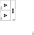
- Fig. 7 shows another schematic diagram of first dedicated pixels 101x and a second dedicated pixel 102.
- Fig. 7 two first dedicated pixels 101x are provided horizontally next to each other, again with a small distance in between.
- the second dedicated pixel 102 is horizontally positioned below the two first dedicated pixels 101x.
- Fig. 7 is an alternative arrangement to the arrangement of Figs. 1 and 2 and can be used in applications, where a rotation of the dedicated pixels 101x, 102 may be beneficial.
- Fig. 8 shows another schematic diagram of a first dedicated pixel 101 and a second dedicated pixel 102.
- the first dedicated pixel is square shaped and has a predetermined edge length 701.
- the second dedicated pixel 102 is rectangular shaped and has a horizontal edge length 702 and a vertical edge length 703.
- the edge length 701 of the first dedicated pixel 101 is approximately half the length of the vertical edge length 703 of the second dedicated pixel 702 and double the length of the horizontal edge length 702 of the second dedicated pixel 702.
- the first dedicated pixel 101 may have an edge length 701 of 50 micrometers to 5 millimeters, especially 100 micrometers to 3 millimeters, and more especially 600 micrometers.
- the second dedicated pixel 102 may have a vertical edge length 703 of 10 micrometers to 10 millimeters, especially 20 micrometers to 6 millimeters, and more especially 1 millimeter, and a horizontal edge length 703 of 10 micrometers to 10 millimeters, especially 30 micrometers to 3 millimeters, and more especially 300 micrometers.
- Fig. 9 shows a flow diagram of an embodiment of an assembly method for a display device 400, 500 for displaying color image data 403, 503.
- the reference signs used in conjunction with Figs. 1 - 6 will be used in the description of Fig. 9 .
- the assembly method comprises providing S1 a plurality of first dedicated pixels 101a, 101b, 101c, 101d, 101x comprising a square shape, and providing S2 a plurality of second dedicated pixels 102 comprising a rectangular shape.
- first dedicated pixels 101a, 101b, 101c, 101d, 101x and the second dedicated pixels 102 are arranged S3 interlaced to form a display surface, wherein each first dedicated pixel 101a, 101b, 101c, 101d, 101x and each second dedicated pixel 102 comprises exactly three light sources of different colors.
- the assembly method can further comprise providing each first dedicated pixel 101a, 101b, 101c, 101d, 101x and each second dedicated pixel 102 with one red light source 101aR, 101bR, 101cR, 101dR, 102R and one green light source 101aG, 101bG, 101cG, 101dG, 102G and one blue light source 101aB, 101bB, 101cB, 101dB, 102B.
- first dedicated pixels 101a, 101b, 101c, 101d, 101x and/or the second dedicated pixels 102 can be provided as integrated surface mount light emitting diodes, SMD-LEDs, with three light sources or as three discrete light emitting diodes, LEDs, wherein the discrete light emitting diodes comprise surface mounted devices, SMD, or through-hole devices.
- two of the first dedicated pixels 101a, 101b, 101c, 101d, 101x can, when vertically positioned adjacent to each other, have the height of one vertically positioned second dedicated pixel 102.
- arranging may comprise positioning two of the first dedicated pixels 101a, 101b, 101c, 101d, 101x vertically positioned adjacent to each other horizontally next to one vertically positioned second dedicated pixel 102.
- Arranging may further comprise providing a pitch between the first dedicated pixels 101a, 101b, 101c, 101d, 101x and/or the second dedicated pixels 102 arranged next to each other that is smaller than five times or four times or three times the edge size of the respective first dedicated pixels 101a, 101b, 101c, 101d, 101x and/or second dedicated pixels 102.
- Arranging may further comprise line-wise arranging the first dedicated pixels 101a, 101b, 101c, 101d, 101x and the second dedicated pixels 102, wherein all the lines 304, 305, 404, 405, 504, 505 may start with two of the first dedicated pixels 101a, 101b, 101c, 101d, 101x vertically positioned adjacent to each other or with one of the second dedicated pixels 102. Further the lines 304, 305, 404, 405, 504, 505 may alternatingly start with two of the first dedicated pixels 101a, 101b, 101c, 101d, 101x vertically positioned adjacent to each other and one of the second dedicated pixels 102.
- providing may comprise providing the first dedicated pixels 101a, 101b, 101c, 101d, 101x with an edge length of 50 micrometers to 5 millimeters, especially 100 micrometers to 3 millimeters, and more especially 600 micrometers, and providing the second dedicated pixels 102 with a vertical edge length of 10 micrometers to 10 millimeters, especially 20 micrometers to 6 millimeters, and more especially 1 millimeter, and providing the second dedicated pixels 102 with a horizontal edge length of 10 micrometers to 10 millimeters, especially 30 micrometers to 3 millimeters, and more especially 300 micrometers.
- providing may comprise providing the first dedicated pixels 101a, 101b, 101c, 101d, 101x with an edge length of 50 micrometers to 5 millimeters, especially 100 micrometers to 3 millimeters, and more especially 600 micrometers, and providing the second dedicated pixels 102 with a vertical edge length of 10 micrometers to 10 millimeters, especially 20 micrometers to 6 millimeters, and more especially 1 millimeter, and providing the second dedicated pixels 102 with a horizontal edge length of 10 micrometers to 10 millimeters, especially 30 micrometers to 3 millimeters, and more especially 300 micrometers.
- the three light sources of the first dedicated pixels 101a, 101b, 101c, 101d, 101x may be provided arranged in a triangle shape. Further, the three light sources in the second dedicated pixels 102 may be arranged in a line arrangement.
Landscapes
- Engineering & Computer Science (AREA)
- Physics & Mathematics (AREA)
- General Physics & Mathematics (AREA)
- Theoretical Computer Science (AREA)
- Computer Hardware Design (AREA)
- Devices For Indicating Variable Information By Combining Individual Elements (AREA)
- Control Of Indicators Other Than Cathode Ray Tubes (AREA)
- Led Device Packages (AREA)
Claims (12)
- Anzeigevorrichtung (400, 500) zur Anzeige von Farbbilddaten (403, 503), wobei die Vorrichtung (400, 500) aufweist:eine Vielzahl von Pixelgruppen, die in einer ersten Richtung und einer zweiten Richtung angeordnet sind, um eine Anzeigefläche zu bilden, wobei die erste Richtung orthogonal zu der zweiten Richtung ist, wobei jede Pixelgruppe aufweistein erstes quadratförmiges Pixelgehäuse (101a, 101c, 101x), ein zweites quadratförmiges Pixelgehäuse (101b, 101d, 101x) und ein rechteckförmiges Pixelgehäuse (102);wobei das erste quadratische Pixelgehäuse (101a, 101c, 101x) und das zweite quadratische Pixelgehäuse (101b, 101d, 101x) gleich groß sind und so angeordnet sind, dass sie in der ersten Richtung mit einem Abstand (a) dazwischen nebeneinander ausgerichtet sind, und das rechteckförmige Pixelgehäuse (102) direkt angrenzend an das erste und das zweite quadratförmige Pixelgehäuse angeordnet und mit diesen in der zweiten Richtung ausgerichtet ist, wobei die Länge der längsten Seite des rechteckförmigen Pixelgehäuses (102) gleich der doppelten Länge einer Seite des ersten quadratförmigen Pixelgehäuses (101a, 101c, 101x) plus dem Abstand (a) ist; undwobei jedes erste quadratförmige Pixelgehäuse (101a, 101c, 101x), jedes zweite quadratförmige Pixelgehäuse (101b, 101d, 101x) und jedes rechteckförmige Pixelgehäuse (102) genau eine rote Lichtquelle (101aR, 101bR, 101cR, 101dR, 102R) und genau eine grüne Lichtquelle (101aG, 101bG, 101cG, 101dG, 102G) und genau eine blaue Lichtquelle (101aB, 101bB, 101cB, 101dB, 102B) aufweist,wobei in jedem der ersten quadratischen Pixelgehäuse (101a, 101c, 101x) und jedem der zweiten quadratischen Pixelgehäuse (101b, 101d, 101x) die drei Lichtquellen jeweils auf einer Ecke einer Dreiecksform angeordnet sind, wobei die Dreiecksform im Wesentlichen im Schwerpunkt jedes der ersten und zweiten quadratischen Pixelgehäuse liegt, und wobei in jedem rechteckigen Pixelgehäuse (102) die drei Lichtquellen in einer zeilenförmigen Anordnung in der ersten Richtung im Schwerpunkt des rechteckigen Pixelgehäuses (102) angeordnet sind.
- Die Anzeigevorrichtung (400, 500) gemäß einem der vorhergehenden Ansprüche, wobei das erste quadratische Pixelgehäuse (101a, 101c, 101x), das zweite quadratische Pixelgehäuse (101b, 101d, 101x) und das rechteckige Pixelgehäuse (102) integrierte oberflächenmontierte Leuchtdioden mit drei Lichtquellen oder drei diskrete Leuchtdioden aufweisen, wobei die diskreten Leuchtdioden oberflächenmontierte Vorrichtungen oder Durchgangslochvorrichtungen aufweisen.
- Anzeigevorrichtung (400, 500) gemäß einem der vorhergehenden Ansprüche,
wobei der Abstand zwischen dem ersten quadratischen Pixelgehäuse (101a, 101c, 101x), dem zweiten quadratischen Pixelgehäuse (101b, 101d, 101x) und/oder dem rechteckigen Pixelgehäuse (102) kleiner als das Fünffache oder das Vierfache oder das Dreifache der Kantengröße des jeweiligen ersten quadratischen Pixelgehäuses (101a, 101c, 101x), zweiten quadratischen Pixelgehäuses (101b, 101d, 101x) und/oder rechteckigen Pixelgehäuses (102) ist. - Die Anzeigevorrichtung (400, 500) gemäß einem der vorhergehenden Ansprüche, die eine zeilenweise Anordnung der Pixelgruppen aufweist.
- Die Anzeigevorrichtung (400, 500) gemäß Anspruch 4, wobei alle Zeilen (304, 305, 404, 405, 504, 505) mit dem ersten quadratischen Pixelgehäuse (101a, 101c, 101x) und dem zweiten quadratischen Pixelgehäuse (101b, 101d, 101x) der jeweiligen Pixelgruppe beginnen oder wobei alle Zeilen (304, 305, 404, 405, 504, 505) mit dem rechteckigen Pixelgehäuse (102) der jeweiligen Pixelgruppe beginnen.
- Die Anzeigevorrichtung (400, 500) gemäß Anspruch 4, wobei die Zeilen (304, 305, 404, 405, 504, 505) abwechselnd mit dem ersten quadratischen Pixelgehäuse (101a, 101c, 101x) und dem zweiten quadratischen Pixelgehäuse (101b, 101d, 101x) der jeweiligen Pixelgruppe oder dem rechteckigen Pixelgehäuse (102) der jeweiligen Pixelgruppe beginnen.
- Die Anzeigevorrichtung (400, 500) gemäß einem der vorhergehenden Ansprüche, wobei das erste quadratische Pixelgehäuse (101a, 101c, 101x) und das zweite quadratische Pixelgehäuse (101b, 101d, 101x) eine Kantenlänge (701) von 50 Mikrometern bis 5 Millimetern, insbesondere 100 Mikrometern bis 3 Millimetern, und insbesondere 600 Mikrometern aufweisen, und wobei das rechteckige Pixelgehäuse (102) eine vertikale Kantenlänge (703) von 10 Mikrometern bis 10 Millimetern, insbesondere 20 Mikrometern bis 6 Millimetern, und insbesondere 1 Millimeter aufweist, und
wobei das rechteckige Pixelgehäuse (102) eine horizontale Kantenlänge (703) von 10 Mikrometern bis 10 Millimetern, insbesondere 30 Mikrometern bis 3 Millimetern und ganz besonders 300 Mikrometern aufweist. - Verfahren zum Zusammenbau einer Anzeigevorrichtung (400, 500) zur Anzeige von Farbbilddaten (403, 503), wobei das Verfahren Folgendes aufweist:Bereitstellen einer Vielzahl von Pixelgruppen, die in einer ersten Richtung und einer zweiten Richtung angeordnet sind, um eine Anzeigefläche zu bilden, wobei die erste Richtung orthogonal zu der zweiten Richtung ist, unddadurch gekennzeichnet, dass:der Schritt des Bereitstellens das Bereitstellen (S1) für jede Pixelgruppe eines ersten quadratischen Pixelgehäuses (101a, 101c, 101x), eines zweiten quadratischen Pixelgehäuses aufweist, undder Schritt des Bereitstellens das Bereitstellen (S2) eines rechteckförmigen Pixelgehäuses (102) für jede Pixelgruppe aufweist, undwobei das erste rechteckförmige Pixelgehäuse (101a, 101c, 101x) und das zweite rechteckförmige Pixelgehäuse (101b, 101d, 101x) in gleicher Größe bereitgestellt werden und so angeordnet sind, dass sie in der ersten Richtung mit einem Abstand (a) dazwischen nebeneinander ausgerichtet sind, und das rechteckförmige Pixelgehäuse (102) direkt neben dem ersten und dem zweiten quadratischen Pixelgehäuse angeordnet und mit diesen in der zweiten Richtung ausgerichtet ist, wobei die Länge der längsten Seite des rechteckförmigen Pixelgehäuses (102) gleich der doppelten Länge einer Seite des ersten quadratischen Pixelgehäuses (101a, 101c, 101x) plus dem Abstand (a) ist; unddas die folgenden weiteren Schritte aufweist:Bereitstellen jedes ersten quadratischen Pixelgehäuses (101a, 101c, 101x), jedes zweiten quadratischen Pixelgehäuses (101b, 101d, 101x) und jedes rechteckigen Pixelgehäuses (102) mit genau einer roten Lichtquelle (101aR, 101bR, 101cR, 101dR, 102R) und genau einer grünen Lichtquelle (101aG, 101bG, 101cG, 101dG, 102G) und genau einer blauen Lichtquelle (101aB, 101bB, 101cB, 101dB, 102B),wobei in jedem der ersten quadratischen Pixelgehäuse (101a, 101c, 101x) und jedem der zweiten quadratischen Pixelgehäuse (101b, 101d, 101x) die drei Lichtquellen jeweils auf einer Ecke einer Dreiecksform angeordnet sind, wobei die Dreiecksform im Wesentlichen im Schwerpunkt jedes der ersten und zweiten quadratischen Pixelgehäuse liegt, und wobei in jedem rechteckigen Pixelgehäuse (102) die drei Lichtquellen in einer zeilenförmigen Anordnung in der ersten Richtung im Schwerpunkt des rechteckigen Pixelgehäuses (102) angeordnet sind.
- Das Verfahren zum Zusammenbau gemäß Anspruch 8, das das Bereitstellen des ersten quadratischen Pixelgehäuses (101a, 101c, 101x), des zweiten quadratischen Pixelgehäuses (101b, 101d, 101x) und des rechteckigen Pixelgehäuses (102) mit integrierten oberflächenmontierten Leuchtdioden mit drei Lichtquellen oder als drei diskrete Leuchtdioden umfasst, wobei die diskreten Leuchtdioden oberflächenmontierte Vorrichtungen oder Durchgangslochvorrichtungen aufweisen.
- Das Verfahren zum Zusammenbau gemäß einem der vorhergehenden Ansprüche 8 und 9,
wobei das erste quadratische Pixelgehäuse (101a, 101c, 101x), das zweite quadratische Pixelgehäuse (101b, 101d, 101x) und/oder das rechteckige Pixelgehäuse (102) mit einem Abstand angeordnet sind, der kleiner als das Fünffache oder das Vierfache oder das Dreifache der Kantengröße des jeweiligen ersten quadratischen Pixelgehäuses (101a, 101c, 101x), zweiten quadratischen Pixelgehäuses (101b, 101d, 101x) und/oder rechteckigen Pixelgehäuses (102) ist. - Das Verfahren zum Zusammenbau gemäß einem der vorhergehenden Ansprüche 8 bis 10, wobei das Anordnen ein zeilenweises Anordnen der Pixelgruppen aufweist, insbesondere wobei alle Zeilen (304, 305, 404, 405, 504, 505) mit dem ersten quadratischen Pixelgehäuse (101a, 101c, 101x) und dem zweiten quadratischen Pixelgehäuse (101b, 101d, 101x) der jeweiligen Pixelgruppe beginnen oder wobei alle Zeilen (304, 305, 404, 405, 504, 505) mit dem rechteckigen Pixelgehäuse (102) der jeweiligen Pixelgruppe beginnen oder wobei die Linien (304, 305, 404, 405, 504, 505) abwechselnd mit dem ersten quadratischen Pixelgehäuse (101a, 101c, 101x) und dem zweiten quadratischen Pixelgehäuse (101b, 101d, 101x) der jeweiligen Pixelgruppe oder dem rechteckigen Pixelgehäuse (102) der jeweiligen Pixelgruppe beginnen.
- Das Verfahren zum Zusammenbau gemäß einem der vorhergehenden Ansprüche 8 bis 11, wobei das erste quadratische Pixelgehäuse (101a, 101c, 101x) und das zweite quadratische Pixelgehäuse (101b, 101d, 101x) mit einer Kantenlänge (701) von 50 Mikrometern bis 5 Millimetern, insbesondere 100 Mikrometern bis 3 Millimetern, und insbesondere 600 Mikrometern bereitgestellt werden, und
wobei das rechteckige Pixelgehäuse (102) mit einer vertikalen Kantenlänge (703) von 10 Mikrometern bis 10 Millimetern, insbesondere 20 Mikrometern bis 6 Millimetern und insbesondere 1 Millimeter, und mit einer horizontalen Kantenlänge (702) von 10 Mikrometern bis 10 Millimetern, insbesondere 30 Mikrometern bis 3 Millimetern und insbesondere 300 Mikrometern, bereitgestellt werden.
Priority Applications (7)
| Application Number | Priority Date | Filing Date | Title |
|---|---|---|---|
| EP16206859.7A EP3343544B1 (de) | 2016-12-28 | 2016-12-28 | Verfahren für eine anzeigevorrichtung |
| TR2017/02847A TR201702847A2 (tr) | 2016-12-28 | 2017-02-24 | Bi̇r görüntü aygiti i̇çi̇n metot |
| JP2019535281A JP7062671B2 (ja) | 2016-12-28 | 2017-09-21 | 表示装置及び組立て方法 |
| US16/474,947 US10867545B2 (en) | 2016-12-28 | 2017-09-21 | Method for a display device |
| PCT/EP2017/073908 WO2018121893A1 (en) | 2016-12-28 | 2017-09-21 | Method for a display device |
| KR1020197020041A KR102451214B1 (ko) | 2016-12-28 | 2017-09-21 | 디스플레이 장치를 위한 방법 |
| CN201780087388.5A CN110337684B (zh) | 2016-12-28 | 2017-09-21 | 用于显示设备的方法 |
Applications Claiming Priority (1)
| Application Number | Priority Date | Filing Date | Title |
|---|---|---|---|
| EP16206859.7A EP3343544B1 (de) | 2016-12-28 | 2016-12-28 | Verfahren für eine anzeigevorrichtung |
Publications (2)
| Publication Number | Publication Date |
|---|---|
| EP3343544A1 EP3343544A1 (de) | 2018-07-04 |
| EP3343544B1 true EP3343544B1 (de) | 2022-06-15 |
Family
ID=57799496
Family Applications (1)
| Application Number | Title | Priority Date | Filing Date |
|---|---|---|---|
| EP16206859.7A Active EP3343544B1 (de) | 2016-12-28 | 2016-12-28 | Verfahren für eine anzeigevorrichtung |
Country Status (7)
| Country | Link |
|---|---|
| US (1) | US10867545B2 (de) |
| EP (1) | EP3343544B1 (de) |
| JP (1) | JP7062671B2 (de) |
| KR (1) | KR102451214B1 (de) |
| CN (1) | CN110337684B (de) |
| TR (1) | TR201702847A2 (de) |
| WO (1) | WO2018121893A1 (de) |
Families Citing this family (18)
| Publication number | Priority date | Publication date | Assignee | Title |
|---|---|---|---|---|
| US11747531B2 (en) | 2016-02-18 | 2023-09-05 | Chengdu Boe Optoelectronics Technology Co., Ltd. | Display substrate, fine metal mask set and manufacturing method thereof |
| US11233096B2 (en) | 2016-02-18 | 2022-01-25 | Boe Technology Group Co., Ltd. | Pixel arrangement structure and driving method thereof, display substrate and display device |
| US11448807B2 (en) | 2016-02-18 | 2022-09-20 | Chengdu Boe Optoelectronics Technology Co., Ltd. | Display substrate, fine metal mask set and manufacturing method thereof |
| CN110137215B (zh) | 2018-02-09 | 2025-01-14 | 京东方科技集团股份有限公司 | 像素排列结构、显示基板和显示装置 |
| CN110137213B (zh) | 2018-02-09 | 2025-03-25 | 京东方科技集团股份有限公司 | 像素排列结构及其显示方法、显示基板 |
| US11574960B2 (en) | 2018-02-09 | 2023-02-07 | Boe Technology Group Co., Ltd. | Pixel arrangement structure, display substrate, display device and mask plate group |
| CN114355678B (zh) | 2018-02-09 | 2023-11-03 | 京东方科技集团股份有限公司 | 显示基板和显示装置 |
| CN113823240B (zh) * | 2018-12-13 | 2023-04-18 | 京东方科技集团股份有限公司 | 显示装置 |
| US11088121B2 (en) * | 2019-02-13 | 2021-08-10 | X Display Company Technology Limited | Printed LED arrays with large-scale uniformity |
| KR102866754B1 (ko) * | 2019-03-04 | 2025-09-30 | 삼성디스플레이 주식회사 | 표시 장치, 표시 장치의 제조장치 및 표시 장치의 제조방법 |
| CN110120188A (zh) * | 2019-03-31 | 2019-08-13 | 深圳市亮彩科技有限公司 | 一种可适应任意角度显示的led显示屏像素排列方式 |
| CN118843353A (zh) | 2019-07-31 | 2024-10-25 | 京东方科技集团股份有限公司 | 显示基板及其制备方法、显示面板、显示装置 |
| EP4006982A4 (de) | 2019-07-31 | 2022-08-03 | BOE Technology Group Co., Ltd. | Anzeigesubstrat und anzeigevorrichtung |
| US11056081B2 (en) * | 2019-08-09 | 2021-07-06 | Wuhan China Star Optoelectronics Semiconductor Display Technology Co., Ltd. | Display panel and display device |
| US11557635B2 (en) | 2019-12-10 | 2023-01-17 | Samsung Display Co., Ltd. | Display device, mask assembly, and apparatus for manufacturing the display device |
| EP3836222A3 (de) | 2019-12-10 | 2021-08-04 | Samsung Display Co., Ltd. | Anzeigevorrichtung, maskenanordnung und vorrichtung zur herstellung einer anzeigevorrichtung |
| US11908881B2 (en) * | 2020-01-21 | 2024-02-20 | Seoul Viosys Co., Ltd. | LED display apparatus having micro LED module |
| US20230215845A1 (en) * | 2020-06-12 | 2023-07-06 | Lg Electronics Inc. | Display device comprising semiconductor light emitting element |
Family Cites Families (32)
| Publication number | Priority date | Publication date | Assignee | Title |
|---|---|---|---|---|
| TW377429B (en) * | 1998-02-11 | 1999-12-21 | Au Optronics Corp | Method of showing graphics on dot matrix display |
| JP3870807B2 (ja) * | 2001-12-20 | 2007-01-24 | ソニー株式会社 | 画像表示装置及びその製造方法 |
| JP2005352408A (ja) * | 2004-06-14 | 2005-12-22 | Sanyo Electric Co Ltd | 表示装置 |
| TWI258721B (en) * | 2004-08-10 | 2006-07-21 | Ind Tech Res Inst | Full-color organic electroluminescence device |
| US7907133B2 (en) * | 2006-04-13 | 2011-03-15 | Daktronics, Inc. | Pixel interleaving configurations for use in high definition electronic sign displays |
| GB2437110B (en) | 2006-04-12 | 2009-01-28 | Cambridge Display Tech Ltd | Optoelectronic display and method of manufacturing the same |
| JP5303834B2 (ja) * | 2006-12-19 | 2013-10-02 | 日亜化学工業株式会社 | 発光装置 |
| JP5311779B2 (ja) * | 2007-08-21 | 2013-10-09 | シチズン電子株式会社 | Led発光装置 |
| JP5215090B2 (ja) * | 2008-02-25 | 2013-06-19 | 三菱電機株式会社 | 画像表示装置及び画像表示装置用表示ユニット |
| CN103559838B (zh) * | 2008-05-11 | 2016-03-23 | Nlt科技股份有限公司 | 非矩形的像素阵列及具有该阵列的显示装置 |
| JP2010206138A (ja) * | 2009-03-06 | 2010-09-16 | Nichia Corp | 発光装置 |
| KR20110013691A (ko) * | 2009-08-03 | 2011-02-10 | 삼성모바일디스플레이주식회사 | 화소구조 및 그를 이용한 유기전계발광표시장치 |
| DE102011053000B4 (de) * | 2010-08-27 | 2017-08-17 | Lg Display Co., Ltd. | Organische elektrolumineszente Vorrichtung |
| US9583034B2 (en) * | 2010-10-15 | 2017-02-28 | Lg Display Co., Ltd. | Subpixel arrangement structure for display device |
| TWI550571B (zh) * | 2011-11-09 | 2016-09-21 | 友達光電股份有限公司 | 立體顯示面板及其驅動方法 |
| EP3780113B1 (de) * | 2012-09-13 | 2025-07-16 | Samsung Display Co., Ltd. | Pixelanordnungsstruktur einer organischen lichtemittierenden diodenanzeige |
| JP2016512344A (ja) * | 2013-03-11 | 2016-04-25 | 深セン市奥拓電子股▲分▼有限公司 | 高解像度ledディスプレイ及びその超微細ドットピッチを有する表面実装型ledコンビネーションランプ |
| US9798372B2 (en) | 2013-06-03 | 2017-10-24 | Qualcomm Incorporated | Devices and methods of sensing combined ultrasonic and infrared signal |
| KR102127762B1 (ko) * | 2013-10-02 | 2020-06-30 | 삼성디스플레이 주식회사 | 평판 표시 장치 |
| CN104885141B (zh) * | 2013-11-04 | 2018-03-16 | 深圳云英谷科技有限公司 | 显示器子像素排布及其渲染方法 |
| CN103903524B (zh) * | 2014-03-25 | 2016-06-15 | 京东方科技集团股份有限公司 | 显示方法 |
| CN103903549B (zh) * | 2014-03-25 | 2016-08-17 | 京东方科技集团股份有限公司 | 显示方法 |
| CN104036700B (zh) * | 2014-05-30 | 2016-02-03 | 京东方科技集团股份有限公司 | 显示面板、显示方法和显示装置 |
| CN104299974B (zh) * | 2014-09-29 | 2017-02-15 | 京东方科技集团股份有限公司 | 阵列基板、掩膜板、显示装置 |
| CN104637987A (zh) * | 2015-02-06 | 2015-05-20 | 友达光电股份有限公司 | 一种主动矩阵有机发光显示器及其像素结构 |
| CN104716163B (zh) * | 2015-03-26 | 2018-03-16 | 京东方科技集团股份有限公司 | 像素结构以及显示基板和显示装置 |
| US9837473B2 (en) * | 2015-04-29 | 2017-12-05 | Lg Display Co., Ltd. | Organic light emitting diode display |
| KR102390473B1 (ko) * | 2015-06-30 | 2022-04-25 | 엘지디스플레이 주식회사 | 표시 패널 및 그를 가지는 표시 장치 |
| CN108155204B (zh) * | 2016-12-02 | 2020-03-17 | 京东方科技集团股份有限公司 | 一种像素排列结构、显示装置及掩膜板 |
| CN108807460B (zh) * | 2017-04-28 | 2019-08-23 | 昆山国显光电有限公司 | 像素结构驱动方法 |
| JP7015324B2 (ja) * | 2017-08-31 | 2022-02-02 | クンシャン ゴー-ビシオノクス オプト-エレクトロニクス カンパニー リミテッド | ピクセル構造、oledディスプレイデバイス、および駆動方法 |
| US20190333434A1 (en) * | 2018-04-29 | 2019-10-31 | Mikro Mesa Technology Co., Ltd. | High fill rate display |
-
2016
- 2016-12-28 EP EP16206859.7A patent/EP3343544B1/de active Active
-
2017
- 2017-02-24 TR TR2017/02847A patent/TR201702847A2/tr unknown
- 2017-09-21 KR KR1020197020041A patent/KR102451214B1/ko active Active
- 2017-09-21 US US16/474,947 patent/US10867545B2/en not_active Expired - Fee Related
- 2017-09-21 JP JP2019535281A patent/JP7062671B2/ja active Active
- 2017-09-21 WO PCT/EP2017/073908 patent/WO2018121893A1/en not_active Ceased
- 2017-09-21 CN CN201780087388.5A patent/CN110337684B/zh not_active Expired - Fee Related
Also Published As
| Publication number | Publication date |
|---|---|
| KR20190097120A (ko) | 2019-08-20 |
| CN110337684B (zh) | 2023-04-04 |
| EP3343544A1 (de) | 2018-07-04 |
| JP2020514792A (ja) | 2020-05-21 |
| WO2018121893A1 (en) | 2018-07-05 |
| KR102451214B1 (ko) | 2022-10-05 |
| US10867545B2 (en) | 2020-12-15 |
| TR201702847A2 (tr) | 2018-07-23 |
| CN110337684A (zh) | 2019-10-15 |
| JP7062671B2 (ja) | 2022-05-06 |
| US20190340970A1 (en) | 2019-11-07 |
Similar Documents
| Publication | Publication Date | Title |
|---|---|---|
| EP3343544B1 (de) | Verfahren für eine anzeigevorrichtung | |
| EP3625502B1 (de) | Mehrfachansichtshintergrundbeleuchtung, anzeige und verfahren mit aktiven emittern | |
| EP3281227B1 (de) | Pixelstruktur, anzeigetafel und anzeigevorrichtung | |
| US10535718B2 (en) | Pixel arrangement of OLED display panel, and OLED display panel | |
| US11309357B2 (en) | Pixel structure, mask and display device with pixel arrangements improving pixels per inch | |
| US10396062B2 (en) | Micro light emitting diode display panel | |
| TWI473074B (zh) | 顯示面板的畫素與子畫素配置 | |
| US11164910B2 (en) | Pixel structures with at least two sub-pixels having a same color | |
| US9799252B2 (en) | Pixel array and driving method thereof, display panel and display device | |
| EP3166098B1 (de) | Pixelanordnung und ansteuerungsverfahren dafür sowie anzeigetafel | |
| US10249259B2 (en) | Method for driving a pixel array | |
| EP3286751B1 (de) | Pixelstruktur, anzeigetafel und anzeigevorrichtung | |
| CN110133885B (zh) | 像素排列结构、显示基板和显示装置 | |
| CN106097898B (zh) | 像素阵列、显示基板和显示装置 | |
| US20200251534A1 (en) | Display panel, display apparatus, and mask plate for fabricating display panel | |
| US20170148365A1 (en) | Color film substrate, display panel and display device thereof | |
| US20200051485A1 (en) | Pixel structure, display substrate, display device and display method | |
| US20230064639A1 (en) | Micro-led pixel arrangement structure, arrangement method, and display panel | |
| US11730029B2 (en) | Display substrate, light field display apparatus and method for driving the same | |
| US9754554B1 (en) | Pixel structure | |
| US10692419B2 (en) | Display panel, display device and display method of display panel | |
| CN104732928A (zh) | 一种像素结构、其驱动方法及显示装置 | |
| CN115810319B (zh) | 一种显示装置 | |
| CN103984163A (zh) | 液晶光栅及显示设备 | |
| US20180045992A1 (en) | Liquid crystal display panel and liquid crystal display device |
Legal Events
| Date | Code | Title | Description |
|---|---|---|---|
| PUAI | Public reference made under article 153(3) epc to a published international application that has entered the european phase |
Free format text: ORIGINAL CODE: 0009012 |
|
| STAA | Information on the status of an ep patent application or granted ep patent |
Free format text: STATUS: THE APPLICATION HAS BEEN PUBLISHED |
|
| AK | Designated contracting states |
Kind code of ref document: A1 Designated state(s): AL AT BE BG CH CY CZ DE DK EE ES FI FR GB GR HR HU IE IS IT LI LT LU LV MC MK MT NL NO PL PT RO RS SE SI SK SM TR |
|
| AX | Request for extension of the european patent |
Extension state: BA ME |
|
| STAA | Information on the status of an ep patent application or granted ep patent |
Free format text: STATUS: REQUEST FOR EXAMINATION WAS MADE |
|
| 17P | Request for examination filed |
Effective date: 20181220 |
|
| RBV | Designated contracting states (corrected) |
Designated state(s): AL AT BE BG CH CY CZ DE DK EE ES FI FR GB GR HR HU IE IS IT LI LT LU LV MC MK MT NL NO PL PT RO RS SE SI SK SM TR |
|
| STAA | Information on the status of an ep patent application or granted ep patent |
Free format text: STATUS: EXAMINATION IS IN PROGRESS |
|
| 17Q | First examination report despatched |
Effective date: 20190405 |
|
| GRAP | Despatch of communication of intention to grant a patent |
Free format text: ORIGINAL CODE: EPIDOSNIGR1 |
|
| STAA | Information on the status of an ep patent application or granted ep patent |
Free format text: STATUS: GRANT OF PATENT IS INTENDED |
|
| INTG | Intention to grant announced |
Effective date: 20220107 |
|
| GRAS | Grant fee paid |
Free format text: ORIGINAL CODE: EPIDOSNIGR3 |
|
| GRAA | (expected) grant |
Free format text: ORIGINAL CODE: 0009210 |
|
| STAA | Information on the status of an ep patent application or granted ep patent |
Free format text: STATUS: THE PATENT HAS BEEN GRANTED |
|
| AK | Designated contracting states |
Kind code of ref document: B1 Designated state(s): AL AT BE BG CH CY CZ DE DK EE ES FI FR GB GR HR HU IE IS IT LI LT LU LV MC MK MT NL NO PL PT RO RS SE SI SK SM TR |
|
| REG | Reference to a national code |
Ref country code: CH Ref legal event code: EP Ref country code: GB Ref legal event code: FG4D |
|
| REG | Reference to a national code |
Ref country code: IE Ref legal event code: FG4D |
|
| REG | Reference to a national code |
Ref country code: DE Ref legal event code: R096 Ref document number: 602016072823 Country of ref document: DE |
|
| REG | Reference to a national code |
Ref country code: AT Ref legal event code: REF Ref document number: 1498851 Country of ref document: AT Kind code of ref document: T Effective date: 20220715 |
|
| REG | Reference to a national code |
Ref country code: LT Ref legal event code: MG9D |
|
| REG | Reference to a national code |
Ref country code: NL Ref legal event code: MP Effective date: 20220615 |
|
| PG25 | Lapsed in a contracting state [announced via postgrant information from national office to epo] |
Ref country code: SE Free format text: LAPSE BECAUSE OF FAILURE TO SUBMIT A TRANSLATION OF THE DESCRIPTION OR TO PAY THE FEE WITHIN THE PRESCRIBED TIME-LIMIT Effective date: 20220615 Ref country code: NO Free format text: LAPSE BECAUSE OF FAILURE TO SUBMIT A TRANSLATION OF THE DESCRIPTION OR TO PAY THE FEE WITHIN THE PRESCRIBED TIME-LIMIT Effective date: 20220915 Ref country code: LT Free format text: LAPSE BECAUSE OF FAILURE TO SUBMIT A TRANSLATION OF THE DESCRIPTION OR TO PAY THE FEE WITHIN THE PRESCRIBED TIME-LIMIT Effective date: 20220615 Ref country code: HR Free format text: LAPSE BECAUSE OF FAILURE TO SUBMIT A TRANSLATION OF THE DESCRIPTION OR TO PAY THE FEE WITHIN THE PRESCRIBED TIME-LIMIT Effective date: 20220615 Ref country code: GR Free format text: LAPSE BECAUSE OF FAILURE TO SUBMIT A TRANSLATION OF THE DESCRIPTION OR TO PAY THE FEE WITHIN THE PRESCRIBED TIME-LIMIT Effective date: 20220916 Ref country code: FI Free format text: LAPSE BECAUSE OF FAILURE TO SUBMIT A TRANSLATION OF THE DESCRIPTION OR TO PAY THE FEE WITHIN THE PRESCRIBED TIME-LIMIT Effective date: 20220615 Ref country code: BG Free format text: LAPSE BECAUSE OF FAILURE TO SUBMIT A TRANSLATION OF THE DESCRIPTION OR TO PAY THE FEE WITHIN THE PRESCRIBED TIME-LIMIT Effective date: 20220915 |
|
| REG | Reference to a national code |
Ref country code: AT Ref legal event code: MK05 Ref document number: 1498851 Country of ref document: AT Kind code of ref document: T Effective date: 20220615 |
|
| PG25 | Lapsed in a contracting state [announced via postgrant information from national office to epo] |
Ref country code: RS Free format text: LAPSE BECAUSE OF FAILURE TO SUBMIT A TRANSLATION OF THE DESCRIPTION OR TO PAY THE FEE WITHIN THE PRESCRIBED TIME-LIMIT Effective date: 20220615 Ref country code: LV Free format text: LAPSE BECAUSE OF FAILURE TO SUBMIT A TRANSLATION OF THE DESCRIPTION OR TO PAY THE FEE WITHIN THE PRESCRIBED TIME-LIMIT Effective date: 20220615 |
|
| PG25 | Lapsed in a contracting state [announced via postgrant information from national office to epo] |
Ref country code: NL Free format text: LAPSE BECAUSE OF FAILURE TO SUBMIT A TRANSLATION OF THE DESCRIPTION OR TO PAY THE FEE WITHIN THE PRESCRIBED TIME-LIMIT Effective date: 20220615 |
|
| PG25 | Lapsed in a contracting state [announced via postgrant information from national office to epo] |
Ref country code: SM Free format text: LAPSE BECAUSE OF FAILURE TO SUBMIT A TRANSLATION OF THE DESCRIPTION OR TO PAY THE FEE WITHIN THE PRESCRIBED TIME-LIMIT Effective date: 20220615 Ref country code: SK Free format text: LAPSE BECAUSE OF FAILURE TO SUBMIT A TRANSLATION OF THE DESCRIPTION OR TO PAY THE FEE WITHIN THE PRESCRIBED TIME-LIMIT Effective date: 20220615 Ref country code: RO Free format text: LAPSE BECAUSE OF FAILURE TO SUBMIT A TRANSLATION OF THE DESCRIPTION OR TO PAY THE FEE WITHIN THE PRESCRIBED TIME-LIMIT Effective date: 20220615 Ref country code: PT Free format text: LAPSE BECAUSE OF FAILURE TO SUBMIT A TRANSLATION OF THE DESCRIPTION OR TO PAY THE FEE WITHIN THE PRESCRIBED TIME-LIMIT Effective date: 20221017 Ref country code: ES Free format text: LAPSE BECAUSE OF FAILURE TO SUBMIT A TRANSLATION OF THE DESCRIPTION OR TO PAY THE FEE WITHIN THE PRESCRIBED TIME-LIMIT Effective date: 20220615 Ref country code: EE Free format text: LAPSE BECAUSE OF FAILURE TO SUBMIT A TRANSLATION OF THE DESCRIPTION OR TO PAY THE FEE WITHIN THE PRESCRIBED TIME-LIMIT Effective date: 20220615 Ref country code: CZ Free format text: LAPSE BECAUSE OF FAILURE TO SUBMIT A TRANSLATION OF THE DESCRIPTION OR TO PAY THE FEE WITHIN THE PRESCRIBED TIME-LIMIT Effective date: 20220615 Ref country code: AT Free format text: LAPSE BECAUSE OF FAILURE TO SUBMIT A TRANSLATION OF THE DESCRIPTION OR TO PAY THE FEE WITHIN THE PRESCRIBED TIME-LIMIT Effective date: 20220615 |
|
| PG25 | Lapsed in a contracting state [announced via postgrant information from national office to epo] |
Ref country code: PL Free format text: LAPSE BECAUSE OF FAILURE TO SUBMIT A TRANSLATION OF THE DESCRIPTION OR TO PAY THE FEE WITHIN THE PRESCRIBED TIME-LIMIT Effective date: 20220615 Ref country code: IS Free format text: LAPSE BECAUSE OF FAILURE TO SUBMIT A TRANSLATION OF THE DESCRIPTION OR TO PAY THE FEE WITHIN THE PRESCRIBED TIME-LIMIT Effective date: 20221015 |
|
| REG | Reference to a national code |
Ref country code: DE Ref legal event code: R097 Ref document number: 602016072823 Country of ref document: DE |
|
| PG25 | Lapsed in a contracting state [announced via postgrant information from national office to epo] |
Ref country code: AL Free format text: LAPSE BECAUSE OF FAILURE TO SUBMIT A TRANSLATION OF THE DESCRIPTION OR TO PAY THE FEE WITHIN THE PRESCRIBED TIME-LIMIT Effective date: 20220615 |
|
| PLBE | No opposition filed within time limit |
Free format text: ORIGINAL CODE: 0009261 |
|
| STAA | Information on the status of an ep patent application or granted ep patent |
Free format text: STATUS: NO OPPOSITION FILED WITHIN TIME LIMIT |
|
| PG25 | Lapsed in a contracting state [announced via postgrant information from national office to epo] |
Ref country code: DK Free format text: LAPSE BECAUSE OF FAILURE TO SUBMIT A TRANSLATION OF THE DESCRIPTION OR TO PAY THE FEE WITHIN THE PRESCRIBED TIME-LIMIT Effective date: 20220615 |
|
| 26N | No opposition filed |
Effective date: 20230316 |
|
| PG25 | Lapsed in a contracting state [announced via postgrant information from national office to epo] |
Ref country code: SI Free format text: LAPSE BECAUSE OF FAILURE TO SUBMIT A TRANSLATION OF THE DESCRIPTION OR TO PAY THE FEE WITHIN THE PRESCRIBED TIME-LIMIT Effective date: 20220615 |
|
| REG | Reference to a national code |
Ref country code: CH Ref legal event code: PL |
|
| REG | Reference to a national code |
Ref country code: BE Ref legal event code: MM Effective date: 20221231 |
|
| PG25 | Lapsed in a contracting state [announced via postgrant information from national office to epo] |
Ref country code: LU Free format text: LAPSE BECAUSE OF NON-PAYMENT OF DUE FEES Effective date: 20221228 |
|
| PG25 | Lapsed in a contracting state [announced via postgrant information from national office to epo] |
Ref country code: LI Free format text: LAPSE BECAUSE OF NON-PAYMENT OF DUE FEES Effective date: 20221231 Ref country code: IE Free format text: LAPSE BECAUSE OF NON-PAYMENT OF DUE FEES Effective date: 20221228 Ref country code: CH Free format text: LAPSE BECAUSE OF NON-PAYMENT OF DUE FEES Effective date: 20221231 |
|
| PG25 | Lapsed in a contracting state [announced via postgrant information from national office to epo] |
Ref country code: FR Free format text: LAPSE BECAUSE OF NON-PAYMENT OF DUE FEES Effective date: 20221231 Ref country code: BE Free format text: LAPSE BECAUSE OF NON-PAYMENT OF DUE FEES Effective date: 20221231 |
|
| PGFP | Annual fee paid to national office [announced via postgrant information from national office to epo] |
Ref country code: GB Payment date: 20231220 Year of fee payment: 8 |
|
| PG25 | Lapsed in a contracting state [announced via postgrant information from national office to epo] |
Ref country code: IT Free format text: LAPSE BECAUSE OF FAILURE TO SUBMIT A TRANSLATION OF THE DESCRIPTION OR TO PAY THE FEE WITHIN THE PRESCRIBED TIME-LIMIT Effective date: 20220615 |
|
| PGFP | Annual fee paid to national office [announced via postgrant information from national office to epo] |
Ref country code: DE Payment date: 20231214 Year of fee payment: 8 |
|
| PG25 | Lapsed in a contracting state [announced via postgrant information from national office to epo] |
Ref country code: HU Free format text: LAPSE BECAUSE OF FAILURE TO SUBMIT A TRANSLATION OF THE DESCRIPTION OR TO PAY THE FEE WITHIN THE PRESCRIBED TIME-LIMIT; INVALID AB INITIO Effective date: 20161228 |
|
| PG25 | Lapsed in a contracting state [announced via postgrant information from national office to epo] |
Ref country code: CY Free format text: LAPSE BECAUSE OF FAILURE TO SUBMIT A TRANSLATION OF THE DESCRIPTION OR TO PAY THE FEE WITHIN THE PRESCRIBED TIME-LIMIT Effective date: 20220615 |
|
| PG25 | Lapsed in a contracting state [announced via postgrant information from national office to epo] |
Ref country code: MK Free format text: LAPSE BECAUSE OF FAILURE TO SUBMIT A TRANSLATION OF THE DESCRIPTION OR TO PAY THE FEE WITHIN THE PRESCRIBED TIME-LIMIT Effective date: 20220615 |
|
| PG25 | Lapsed in a contracting state [announced via postgrant information from national office to epo] |
Ref country code: MC Free format text: LAPSE BECAUSE OF FAILURE TO SUBMIT A TRANSLATION OF THE DESCRIPTION OR TO PAY THE FEE WITHIN THE PRESCRIBED TIME-LIMIT Effective date: 20220615 |
|
| PG25 | Lapsed in a contracting state [announced via postgrant information from national office to epo] |
Ref country code: MC Free format text: LAPSE BECAUSE OF FAILURE TO SUBMIT A TRANSLATION OF THE DESCRIPTION OR TO PAY THE FEE WITHIN THE PRESCRIBED TIME-LIMIT Effective date: 20220615 |
|
| PG25 | Lapsed in a contracting state [announced via postgrant information from national office to epo] |
Ref country code: MT Free format text: LAPSE BECAUSE OF FAILURE TO SUBMIT A TRANSLATION OF THE DESCRIPTION OR TO PAY THE FEE WITHIN THE PRESCRIBED TIME-LIMIT Effective date: 20220615 |
|
| PG25 | Lapsed in a contracting state [announced via postgrant information from national office to epo] |
Ref country code: BG Free format text: LAPSE BECAUSE OF FAILURE TO SUBMIT A TRANSLATION OF THE DESCRIPTION OR TO PAY THE FEE WITHIN THE PRESCRIBED TIME-LIMIT Effective date: 20220615 |
|
| PG25 | Lapsed in a contracting state [announced via postgrant information from national office to epo] |
Ref country code: BG Free format text: LAPSE BECAUSE OF FAILURE TO SUBMIT A TRANSLATION OF THE DESCRIPTION OR TO PAY THE FEE WITHIN THE PRESCRIBED TIME-LIMIT Effective date: 20220615 |
|
| REG | Reference to a national code |
Ref country code: DE Ref legal event code: R119 Ref document number: 602016072823 Country of ref document: DE |
|
| GBPC | Gb: european patent ceased through non-payment of renewal fee |
Effective date: 20241228 |
|
| PG25 | Lapsed in a contracting state [announced via postgrant information from national office to epo] |
Ref country code: DE Free format text: LAPSE BECAUSE OF NON-PAYMENT OF DUE FEES Effective date: 20250701 |
|
| PG25 | Lapsed in a contracting state [announced via postgrant information from national office to epo] |
Ref country code: GB Free format text: LAPSE BECAUSE OF NON-PAYMENT OF DUE FEES Effective date: 20241228 |
|
| PGFP | Annual fee paid to national office [announced via postgrant information from national office to epo] |
Ref country code: TR Payment date: 20251219 Year of fee payment: 10 |