EP3343565B1 - Schieberegister, gatetreiberschaltung und zugehörige anzeigevorrichtung - Google Patents
Schieberegister, gatetreiberschaltung und zugehörige anzeigevorrichtung Download PDFInfo
- Publication number
- EP3343565B1 EP3343565B1 EP16808897.9A EP16808897A EP3343565B1 EP 3343565 B1 EP3343565 B1 EP 3343565B1 EP 16808897 A EP16808897 A EP 16808897A EP 3343565 B1 EP3343565 B1 EP 3343565B1
- Authority
- EP
- European Patent Office
- Prior art keywords
- node
- switch transistor
- potential
- signal
- input
- Prior art date
- Legal status (The legal status is an assumption and is not a legal conclusion. Google has not performed a legal analysis and makes no representation as to the accuracy of the status listed.)
- Active
Links
Images





Classifications
-
- G—PHYSICS
- G09—EDUCATION; CRYPTOGRAPHY; DISPLAY; ADVERTISING; SEALS
- G09G—ARRANGEMENTS OR CIRCUITS FOR CONTROL OF INDICATING DEVICES USING STATIC MEANS TO PRESENT VARIABLE INFORMATION
- G09G3/00—Control arrangements or circuits, of interest only in connection with visual indicators other than cathode-ray tubes
- G09G3/20—Control arrangements or circuits, of interest only in connection with visual indicators other than cathode-ray tubes for presentation of an assembly of a number of characters, e.g. a page, by composing the assembly by combination of individual elements arranged in a matrix no fixed position being assigned to or needed to be assigned to the individual characters or partial characters
- G09G3/22—Control arrangements or circuits, of interest only in connection with visual indicators other than cathode-ray tubes for presentation of an assembly of a number of characters, e.g. a page, by composing the assembly by combination of individual elements arranged in a matrix no fixed position being assigned to or needed to be assigned to the individual characters or partial characters using controlled light sources
- G09G3/30—Control arrangements or circuits, of interest only in connection with visual indicators other than cathode-ray tubes for presentation of an assembly of a number of characters, e.g. a page, by composing the assembly by combination of individual elements arranged in a matrix no fixed position being assigned to or needed to be assigned to the individual characters or partial characters using controlled light sources using electroluminescent panels
- G09G3/32—Control arrangements or circuits, of interest only in connection with visual indicators other than cathode-ray tubes for presentation of an assembly of a number of characters, e.g. a page, by composing the assembly by combination of individual elements arranged in a matrix no fixed position being assigned to or needed to be assigned to the individual characters or partial characters using controlled light sources using electroluminescent panels semiconductive, e.g. using light-emitting diodes [LED]
- G09G3/3208—Control arrangements or circuits, of interest only in connection with visual indicators other than cathode-ray tubes for presentation of an assembly of a number of characters, e.g. a page, by composing the assembly by combination of individual elements arranged in a matrix no fixed position being assigned to or needed to be assigned to the individual characters or partial characters using controlled light sources using electroluminescent panels semiconductive, e.g. using light-emitting diodes [LED] organic, e.g. using organic light-emitting diodes [OLED]
- G09G3/3266—Details of drivers for scan electrodes
-
- G—PHYSICS
- G09—EDUCATION; CRYPTOGRAPHY; DISPLAY; ADVERTISING; SEALS
- G09G—ARRANGEMENTS OR CIRCUITS FOR CONTROL OF INDICATING DEVICES USING STATIC MEANS TO PRESENT VARIABLE INFORMATION
- G09G3/00—Control arrangements or circuits, of interest only in connection with visual indicators other than cathode-ray tubes
- G09G3/20—Control arrangements or circuits, of interest only in connection with visual indicators other than cathode-ray tubes for presentation of an assembly of a number of characters, e.g. a page, by composing the assembly by combination of individual elements arranged in a matrix no fixed position being assigned to or needed to be assigned to the individual characters or partial characters
- G09G3/22—Control arrangements or circuits, of interest only in connection with visual indicators other than cathode-ray tubes for presentation of an assembly of a number of characters, e.g. a page, by composing the assembly by combination of individual elements arranged in a matrix no fixed position being assigned to or needed to be assigned to the individual characters or partial characters using controlled light sources
- G09G3/30—Control arrangements or circuits, of interest only in connection with visual indicators other than cathode-ray tubes for presentation of an assembly of a number of characters, e.g. a page, by composing the assembly by combination of individual elements arranged in a matrix no fixed position being assigned to or needed to be assigned to the individual characters or partial characters using controlled light sources using electroluminescent panels
- G09G3/32—Control arrangements or circuits, of interest only in connection with visual indicators other than cathode-ray tubes for presentation of an assembly of a number of characters, e.g. a page, by composing the assembly by combination of individual elements arranged in a matrix no fixed position being assigned to or needed to be assigned to the individual characters or partial characters using controlled light sources using electroluminescent panels semiconductive, e.g. using light-emitting diodes [LED]
- G09G3/3208—Control arrangements or circuits, of interest only in connection with visual indicators other than cathode-ray tubes for presentation of an assembly of a number of characters, e.g. a page, by composing the assembly by combination of individual elements arranged in a matrix no fixed position being assigned to or needed to be assigned to the individual characters or partial characters using controlled light sources using electroluminescent panels semiconductive, e.g. using light-emitting diodes [LED] organic, e.g. using organic light-emitting diodes [OLED]
- G09G3/3225—Control arrangements or circuits, of interest only in connection with visual indicators other than cathode-ray tubes for presentation of an assembly of a number of characters, e.g. a page, by composing the assembly by combination of individual elements arranged in a matrix no fixed position being assigned to or needed to be assigned to the individual characters or partial characters using controlled light sources using electroluminescent panels semiconductive, e.g. using light-emitting diodes [LED] organic, e.g. using organic light-emitting diodes [OLED] using an active matrix
- G09G3/3233—Control arrangements or circuits, of interest only in connection with visual indicators other than cathode-ray tubes for presentation of an assembly of a number of characters, e.g. a page, by composing the assembly by combination of individual elements arranged in a matrix no fixed position being assigned to or needed to be assigned to the individual characters or partial characters using controlled light sources using electroluminescent panels semiconductive, e.g. using light-emitting diodes [LED] organic, e.g. using organic light-emitting diodes [OLED] using an active matrix with pixel circuitry controlling the current through the light-emitting element
- G09G3/3241—Control arrangements or circuits, of interest only in connection with visual indicators other than cathode-ray tubes for presentation of an assembly of a number of characters, e.g. a page, by composing the assembly by combination of individual elements arranged in a matrix no fixed position being assigned to or needed to be assigned to the individual characters or partial characters using controlled light sources using electroluminescent panels semiconductive, e.g. using light-emitting diodes [LED] organic, e.g. using organic light-emitting diodes [OLED] using an active matrix with pixel circuitry controlling the current through the light-emitting element the current through the light-emitting element being set using a data current provided by the data driver, e.g. by using a two-transistor current mirror
- G09G3/325—Control arrangements or circuits, of interest only in connection with visual indicators other than cathode-ray tubes for presentation of an assembly of a number of characters, e.g. a page, by composing the assembly by combination of individual elements arranged in a matrix no fixed position being assigned to or needed to be assigned to the individual characters or partial characters using controlled light sources using electroluminescent panels semiconductive, e.g. using light-emitting diodes [LED] organic, e.g. using organic light-emitting diodes [OLED] using an active matrix with pixel circuitry controlling the current through the light-emitting element the current through the light-emitting element being set using a data current provided by the data driver, e.g. by using a two-transistor current mirror the data current flowing through the driving transistor during a setting phase, e.g. by using a switch for connecting the driving transistor to the data driver
-
- G—PHYSICS
- G09—EDUCATION; CRYPTOGRAPHY; DISPLAY; ADVERTISING; SEALS
- G09G—ARRANGEMENTS OR CIRCUITS FOR CONTROL OF INDICATING DEVICES USING STATIC MEANS TO PRESENT VARIABLE INFORMATION
- G09G3/00—Control arrangements or circuits, of interest only in connection with visual indicators other than cathode-ray tubes
- G09G3/20—Control arrangements or circuits, of interest only in connection with visual indicators other than cathode-ray tubes for presentation of an assembly of a number of characters, e.g. a page, by composing the assembly by combination of individual elements arranged in a matrix no fixed position being assigned to or needed to be assigned to the individual characters or partial characters
- G09G3/34—Control arrangements or circuits, of interest only in connection with visual indicators other than cathode-ray tubes for presentation of an assembly of a number of characters, e.g. a page, by composing the assembly by combination of individual elements arranged in a matrix no fixed position being assigned to or needed to be assigned to the individual characters or partial characters by control of light from an independent source
- G09G3/36—Control arrangements or circuits, of interest only in connection with visual indicators other than cathode-ray tubes for presentation of an assembly of a number of characters, e.g. a page, by composing the assembly by combination of individual elements arranged in a matrix no fixed position being assigned to or needed to be assigned to the individual characters or partial characters by control of light from an independent source using liquid crystals
- G09G3/3611—Control of matrices with row and column drivers
- G09G3/3674—Details of drivers for scan electrodes
- G09G3/3677—Details of drivers for scan electrodes suitable for active matrices only
-
- G—PHYSICS
- G11—INFORMATION STORAGE
- G11C—STATIC STORES
- G11C19/00—Digital stores in which the information is moved stepwise, e.g. shift registers
- G11C19/28—Digital stores in which the information is moved stepwise, e.g. shift registers using semiconductor elements
-
- G—PHYSICS
- G11—INFORMATION STORAGE
- G11C—STATIC STORES
- G11C19/00—Digital stores in which the information is moved stepwise, e.g. shift registers
- G11C19/28—Digital stores in which the information is moved stepwise, e.g. shift registers using semiconductor elements
- G11C19/287—Organisation of a multiplicity of shift registers
-
- G—PHYSICS
- G09—EDUCATION; CRYPTOGRAPHY; DISPLAY; ADVERTISING; SEALS
- G09G—ARRANGEMENTS OR CIRCUITS FOR CONTROL OF INDICATING DEVICES USING STATIC MEANS TO PRESENT VARIABLE INFORMATION
- G09G2300/00—Aspects of the constitution of display devices
- G09G2300/08—Active matrix structure, i.e. with use of active elements, inclusive of non-linear two terminal elements, in the pixels together with light emitting or modulating elements
- G09G2300/0809—Several active elements per pixel in active matrix panels
-
- G—PHYSICS
- G09—EDUCATION; CRYPTOGRAPHY; DISPLAY; ADVERTISING; SEALS
- G09G—ARRANGEMENTS OR CIRCUITS FOR CONTROL OF INDICATING DEVICES USING STATIC MEANS TO PRESENT VARIABLE INFORMATION
- G09G2310/00—Command of the display device
- G09G2310/02—Addressing, scanning or driving the display screen or processing steps related thereto
- G09G2310/0264—Details of driving circuits
- G09G2310/0286—Details of a shift registers arranged for use in a driving circuit
-
- G—PHYSICS
- G09—EDUCATION; CRYPTOGRAPHY; DISPLAY; ADVERTISING; SEALS
- G09G—ARRANGEMENTS OR CIRCUITS FOR CONTROL OF INDICATING DEVICES USING STATIC MEANS TO PRESENT VARIABLE INFORMATION
- G09G2310/00—Command of the display device
- G09G2310/08—Details of timing specific for flat panels, other than clock recovery
-
- G—PHYSICS
- G09—EDUCATION; CRYPTOGRAPHY; DISPLAY; ADVERTISING; SEALS
- G09G—ARRANGEMENTS OR CIRCUITS FOR CONTROL OF INDICATING DEVICES USING STATIC MEANS TO PRESENT VARIABLE INFORMATION
- G09G2320/00—Control of display operating conditions
- G09G2320/06—Adjustment of display parameters
- G09G2320/0626—Adjustment of display parameters for control of overall brightness
- G09G2320/0633—Adjustment of display parameters for control of overall brightness by amplitude modulation of the brightness of the illumination source
-
- G—PHYSICS
- G09—EDUCATION; CRYPTOGRAPHY; DISPLAY; ADVERTISING; SEALS
- G09G—ARRANGEMENTS OR CIRCUITS FOR CONTROL OF INDICATING DEVICES USING STATIC MEANS TO PRESENT VARIABLE INFORMATION
- G09G2320/00—Control of display operating conditions
- G09G2320/06—Adjustment of display parameters
- G09G2320/0626—Adjustment of display parameters for control of overall brightness
- G09G2320/064—Adjustment of display parameters for control of overall brightness by time modulation of the brightness of the illumination source
Definitions
- the present invention relates to a shift register, a gate driving circuit comprising multiple of the shift registers, an organic light-emitting display (OLED) panel comprising the gate driving circuit, and a display device comprising the OLED panel.
- OLED organic light-emitting display
- Gate Driver on Array (GOA) technique integrates a thin film transistor (TFT) gate switching circuit on an array substrate of a display panel to form scanning drive of the display panel, so that wiring space of bonding region and fan-out region of a gate integrated circuit (IC) could be saved. It could not only reduce products' cost on material and manufacturing process, but also enable the display panel to realize an artistic design with symmetrical on both sides and narrow frame. Furthermore, such integration process could also spare bonding process in a direction of gate scanning line, so as to raise productivity and yield rate.
- TFT thin film transistor
- the GOA circuit is generally composed of multiple shift registers connected in cascades.
- a driving signal output terminal of each stage of shift register is corresponding to one gate line respectively and is used to arrange respective gate lines along a scanning direction sequentially.
- scanning time length for each row of gate lines is generally fixed. Therefore, the existing GOA circuit is not suitable for use in some display devices that need to adjust the scanning time length of each row of gate lines according to actual situation.
- CN 104 835 450 A discloses a shift register unit comprising a signal input module, a pull-down module, a pull-up module, a first pull-up control module, and a second pull-up control module.
- the signal input module is connected with a signal input end, a first clock signal end, and a control node.
- the pull-down module is connected with the control node, a first voltage end, and a signal output end.
- the first pull-up control module is connected with the control node, the pull-up module, and a second voltage end.
- the second pull-up control module is connected with the control node, the pull-up module, a first clock signal end, a first voltage end, and a second clock signal end.
- the pull-up module is also connected with a signal output end and the second voltage end.
- CN 104 835 531 A discloses a shift register unit and a shift register comprising multiple stages of the shift register units.
- CN 104 537 979 A discloses register comprising a first control module, a second control module, an output module and an input module, wherein the first control module is connected with an on-state voltage incoming end and a first node and used for controlling whether on-state voltage and a first control signal are output to the first node or not; the second control module is connected with the on-state voltage incoming end, a second node and an output end and used for controlling whether the on-state voltage and the voltage of the output end are output to the second node or not; the output module is connected with the first node, the second node, the output end, an off-state voltage incoming end and the on-state voltage incoming end and used for inputting the on-state voltage or off-state voltage to the output end according to the voltage of the first node and the second node; and the input module is connected with an input end and used for controlling whether a signal of the input end is input to the first control module and the second control module or not.
- the shift register, the gate driving circuit and the relevant display device comprise: the first node controlling module, the second node controlling module, the third node controlling module, the first outputting module, and the second outputting module, wherein the first node controlling module adjusts the potential of the first node through the input signal, the first clock signal, the second clock signal, the first direct current signal and the potential of the second node, the second node controlling module adjusts the potential of the second node through the first clock signal, the second clock signal, the first direct current signal, the second direct current signal and the potential of the first node, the third node controlling module adjusts the potential of the third node through the second clock signal, the second direct current signal, the potential of the first node and the potential of the second node, the first outputting module adjusts the potential of the driving signal output terminal through the second direct current signal and the potential of the first node, and the second outputting module adjusts the potential of the driving signal output terminal though the first direct current signal and the potential of the third node.
- the shift register could control the time length of the scanning signal outputted by the driving signal output terminal by only changing the time length of the input signal, without changing the clock signals, and changing the circuit and changing the process. Therefore, compared with the prior art where the time length of the scanning signal outputted by the driving signal output terminal is controlled by using various clock control signals, the present disclosure could reduce the difficulty of the gate driving circuit and solve the problem of process complexity, so as to reduce cost.
- Fig.1 shows a schematic diagram of a structure provided in an embodiment of the present disclosure.
- the shift register comprises: a first node controlling module 1, a second node controlling module 2, a third node controlling module 3, a first outputting module 4 and a second outputting module 5.
- an input terminal of the first node controlling module 1 is used to receive an input signal Input
- a second input terminal thereof is used to receive a first clock signal CK
- a third input terminal thereof is used to receive a second clock signal CB
- a fourth input terminal thereof is used to receive a first direct current signal V1
- a fifth input terminal thereof is connected to a second node B
- an output terminal thereof is connected to a first node A
- the first node controlling module 1 is configured to provide the input signal Input to the first node A when a potential of the first clock signal CK is a first potential, provide the first direct current signal V1 to the first node A when both a potential of the second clock signal CB and a potential of the second node B are the first potential, and maintain a voltage difference between the third input terminal and the first node A to a voltage difference of a previous period of time when the first node A is in a floating status;
- a first input terminal of the second node controlling module 2 is used to receive a second direct current signal V2, a second input terminal thereof is used to receive a first clock signal CK, a third input terminal thereof is used to receive a second clock signal CB, a fourth input terminal thereof is connected to the first node A, and an output terminal thereof is connected to the second node B; and the second node controlling module 2 is configured to provide the second direct current signal V2 to the second node B when a potential of the first clock signal CK is a first potential, provide the first clock signal CK to the second node B when a potential of the first node A is the first potential, and maintain a voltage difference between the third input terminal and the second node B to a voltage difference of the previous period of time when the second node B is in a floating status;
- a first input terminal of the third node controlling module 3 is used to receive the second clock signal CB, a second input terminal thereof is used to receive the first direct current signal V1, a third input terminal thereof is used to receive the second direct current signal V2, a fourth input terminal thereof is connected to the first node A, a fifth input terminal thereof is connected to the second node B, and an output terminal thereof is connected to a third node C; and the third node controlling module 3 is configured to provide the first direct current signal V1 to the third node C when the potential of the first node A is the first potential, provide the second direct current signal V2 to the third node C when both the potential of the second clock signal CB and the potential of the second node B are the first potential, and maintain a voltage difference between the second input terminal and the third node C to a voltage difference of the previous period of time when the third node C is in a floating status;
- a first input terminal of the first outputting module 4 is used to receive the second direct current signal V2, a second input terminal thereof is connected to the first node A, and an output terminal thereof is connected to a driving signal output terminal Output of the shift register; and the first outputting module 4 is configured to provide the second direct current signal V2 to the driving signal output terminal Output when the potential of the first node A is the first potential.
- a first input terminal of the second output module 5 is used to receive the first direct current signal V1, a second input terminal thereof is connected to the third node C, and an output terminal thereof is connected to the driving signal output terminal Output of the shift register; and the second output module 5 is configured to provide the first direct current signal V1 to the driving signal output terminal Output when the potential of the third node C is the first potential.
- the first potential is a low potential
- the potential of the first direct current signal V1 is a high potential
- the potential of the second direct current signal V2 is a low potential
- the first potential is a high potential
- the potential of the first direct current signal V1 is a low potential
- the potential of the second direct current signal V2 is a high potential
- the shift register, the gate driving circuit and the relevant display device comprise: the first node controlling module, the second node controlling module, the third node controlling module, the first outputting module, and the second outputting module, wherein the first node controlling module adjusts the potential of the first node through the input signal, the first clock signal, the second clock signal, the first direct current signal and the potential of the second node, the second node controlling module adjusts the potential of the second node through the first clock signal, the second clock signal, the first direct current signal, the second direct current signal and the potential of the first node, the third node controlling module adjusts the potential of the third node through the second clock signal, the second direct current signal, the potential of the first node and the potential of the second node, the first outputting module adjusts the potential of the driving signal output terminal through the second direct current signal and the potential of the first node, and the second outputting module adjusts the potential of the driving signal output terminal though the first direct current signal and the potential of the third node.
- the shift register could control the time length of the scanning signal outputted by the driving signal output terminal by only changing the time length of the input signal, without changing the clock signal, changing the circuit and changing the process. Therefore, compared with the prior art where the time length of the scanning signal outputted by the driving signal output terminal is controlled by using various clock control signals, the present disclosure could reduce difficulty of the gate driving circuit and solve problem of process complexity, so as to reduce cost.
- the first clock signal and the second clock signal have a same cycle and a same duty ratio, and the duty ratio is greater than 0.5; or, when the valid pulse signal of the input signal is a low potential, the falling edge of the input signal aligns with the rising edge of the first clock signal and the falling edge of the second clock signal, and the rising edge of the input signal aligns with the falling edge of the first clock signal.
- the first clock signal and the second clock signal have a same cycle and a same duty ratio, and the duty ratio is smaller than 0.5.
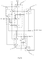
- Figs.2a and 2b show schematic diagram of exemplary structures of a shift register provided in an embodiment of the present disclosure.
- the first node controlling module 1 can comprise: a first switch transistor T1, a second switch transistor T2, a third switch transistor T3 and a first capacitor C1.
- a gate of the first switch transistor T1 is used to receive the first clock signal CK, a source thereof is used to receive the input signal Input, and a drain thereof is connected to the first node A.
- a gate of the second switch transistor T2 is connected to the second node B, a source thereof is used to receive the first direct current signal V1, and a drain thereof is connected to a source of the third switch transistor T3.
- a gate of the third switch transistor T3 is used to receive the second clock signal CB, and a drain thereof is connected to the first node A.
- One terminal of the first capacitor C1 is connected to the first node A, and another terminal thereof is used to receive the second clock signal CB.
- the first switch transistor T1, the second switch transistor T2 and the third switch transistor T3 could be P type transistors.
- the first switch transistor T1, the second switch transistor T2 and the third switch transistor T3 could be N type transistor, to which no limitation is given.
- the input signal Input is provided to the first node A.
- the second switch transistor T2 is in the turn-on state under the control of the potential of the second node B and the third switch transistor T3 is in the turn-on state under the control of the second clock signal CB
- the first direct current signal V1 is provided to the first node A.
- the first node A is in a floating state, according to bootstrap effect of the first capacitor C1, a voltage difference between the third input terminal of the first node controlling module 1 and the first node A is maintained to a voltage difference of the previous period of time.
- the specific structure of the first node control module 1 is not limited to the above structure provided in the embodiment of the present disclosure, but could be other structures known by those skilled in the art, to which no limitation is given herein.
- the second node controlling module can comprise: a fourth switch transistor T4, a fifth switch transistor T5 and a second capacitor C2.
- a gate of the fourth switch transistor T4 is connected to the first node A, a source thereof is used to receive the first clock signal CK, and a drain thereof is connected to the second node B.
- a gate of the fifth switch transistor T5 is used to receive the first clock signal CK, a source thereof is used to receive the second direct current signal V2, and a drain thereof is connected to the second node B.
- One terminal of the second capacitor C2 is connected to the second node B, and the other terminal thereof is used to receive the second clock signal CB.
- both the fourth switch transistor T4 and the fifth switch transistor T5 are P type transistors.
- both the fourth switch transistor T4 and the fifth switch transistor T5 could be N type transistor, to which no limitation is given herein.
- the fourth switch transistor T4 when the fourth switch transistor T4 is in the turn-on state under the control of the first node A, the first clock signal CK is provided to the second node B; when the fifth switch transistor T5 is in the turn-on stage under the control of the first clock signal CK, the second direct current signal V2 is provided to the second node B; and when the second node B is in a floating state, according to bootstrap effect of the second capacitor C2, a voltage difference between the third input terminal of the second node controlling module 2 and the second node B is maintained to a voltage difference of the previous period of time.
- the above description just explains the specific structure of the second node controlling module in the shift register by taking examples.
- the specific structure of the second node control module is not limited to the above structure provided in the embodiment of the present disclosure, but could be other structures known by those skilled in the art, to which no limitation is given herein.
- the third node controlling module 3 could comprise: a sixth switch transistor T6, a seventh switch transistor T7, an eighth switch transistor T8 and a third capacitor C3.
- a gate of the sixth switch transistor T6 is connected to the second node B, a source thereof is used to receive the second direct current signal V2, and a drain thereof is connected to a source of the seventh switch transistor T7.
- a gate of the seventh switch transistor T7 is used to receive the second clock signal CB, and a drain thereof is connected to the third node C.
- a gate of the eighth switch transistor T8 is connected to the first node A, a source thereof is used to receive the first direct current signal V1, and a drain thereof is connected to the third node C.
- One terminal of the third capacitor C3 is connected to the third node C, and the other terminal is used to receive the first direct current signal V1.
- the sixth switch transistor T6, the seventh switch transistor T7, and the eighth switch transistor T8 could be P type transistors.
- the sixth switch transistor T6, the seventh switch transistor T7, and the eighth switch transistor T8 could be N type transistors, to which no limitation is given.
- the second direct current signal V2 is provided to the third node C; and when the third node C is in a floating state, according to the bootstrap effect of the third capacitor C3, a voltage difference between the second input terminal of the third node controlling module 3 and the third node C is maintained to a voltage difference of the previous period of time.
- the specific structure of the third node control module is not limited to the above structure provided in the embodiment of the present disclosure, but could be other structures known by those skilled in the art, to which no limitation is given herein.
- the first outputting module 4 could comprise: a ninth switch transistor T9.
- a gate of the ninth switch transistor T9 is connected to the first node A, a source thereof is used to receive the second direct current signal V2, and a drain thereof is connected to the driving signal output terminal Output.
- the ninth switch transistor T9 could be a P type transistor. Or, as shown in Fig.2b , the ninth switch transistor T9 could be an N type transistor, to which no limitation is given herein.
- the ninth switch transistor T9 when the ninth switch transistor T9 is in the turn-on state under the control of the potential of the first node A, the second direct current signal V2 is provided to the driving signal output terminal Output.
- the specific structure of the first outputting module is not limited to the above structure provided in the embodiment of the present disclosure, but could be other structures known by those skilled in the art, to which no limitation is given herein.
- the second output module 5 could comprise: a tenth switch transistor T10.
- a gate of the tenth switch transistor T10 is connected to the third node C, a source thereof is used to receive the first direct current signal V1, and a drain thereof is connected to the driving signal output terminal Output.
- the tenth switch transistor T10 could be a P type transistor. Or, as shown in Fig.2b , the tenth switch transistor T10 could be an N type transistor, to which no limitation is given herein.
- the first direct current signal V1 is provided to the driving signal output terminal Output.
- transistors generally adopt a same material.
- all the switch transistors are P type transistors, and the potential of the first direct current signal is the high potential, and the potential of the second direct current signal is the low potential; and when the valid pulse signal of the input signal is the low potential, all the switch transistors are N type transistors, and the potential of the first direct current signal is the low potential, the potential of the second direct current signal is the high potential.
- the P type transistor is turned off under the effect of the high potential and turned on under the effect of the low potential; the N type switch transistor is turned on under the effect of the high potential and turned off under the effect of the low potential.
- switch transistors mentioned in the above embodiments of the present disclosure could be thin film transistors (TFT), or could be metal oxide semiconductors (MOS), to which no limitation is given herein.
- TFT thin film transistors
- MOS metal oxide semiconductors
- functions of sources and drains of these transistors could be exchanged with each other depending on different types of transistors and input signals, to which no specific distinction is made herein.
- the shift register is described by taking the structure of the shift register as shown in Fig.2a as an example.
- all of the switch transistors are P type transistors.
- the respective P type transistors are turned off under the effect of the high potential and turned on under the effect of the low potential.
- the first clock signal CK and the second clock signal CB have the same cycle and same duty ratio, and the duty ratio of both the first clock signal CK and the second clock signal CB are greater than 0.5.
- the potential of the first direct current signal V1 is the high potential
- the potential of the second direct current signal V2 is the low potential.
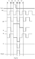
- the corresponding input/output timing diagram is as shown in Fig.3a . In particular, five phases S1, S2, S3, S4 and S5 in the input/output timing diagram as shown in Fig.3a are selected.
- the second switch transistor T2 and the sixth switch transistor T6 are turned off. Since the eighth transistor T8 is turned on, the potential of the first direct current signal V1 is provided to the third node C, the potential of the third node C is the high potential. Since the potential of the third node C is the high potential, the tenth switch transistor T10 is turned off. Since the ninth switch transistor T9 is turned on and provides the second direct current signal V2 to the driving signal output terminal Output, the driving signal output terminal Output outputs the scanning signal with the low potential.
- the first clock signal CK with the high potential is provided to the first node A through the second switch transistor T2 and the third switch transistor T3, and thus the potential of the first node A is the high potential. Since the potential of the first node A is the high potential, the fourth switch transistor T4, the eighth switch transistor T8 and the ninth switch transistor T9 are turned off. Since both the sixth switch transistor T6 and the seventh transistor T7 are turned on and provide the second direct current signal V2 to the third node C through the sixth switch transistor T6 and the seventh transistor T7, the potential of the third node C is the low potential, and thus the third capacitor C3 starts to be charged.
- the tenth switch transistor T10 Since the potential of the third node C is the low potential, the tenth switch transistor T10 is turned on. Since the tenth switch transistor T10 is turned on and provides the first direct current signal V1 to the driving signal output terminal Output, the driving signal output terminal Output outputs the scanning signal with the high potential.
- phase S5 the shift register provided in the embodiment of the present disclosure keeps repeating execution of phases S2 and S1 until the next frame starts.
- the operation process of the shift register is described by taking the structure of the shift register as shown in Fig.2a as an example.
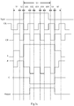
- the time length of the valid pulse signal of the input signal Input is prolonged one clock signal cycle, and its corresponding input/output timing diagram is as shown in Fig.3b .
- five phases S1, S2, S3, S4, and S5 in the input/output timing diagram as shown in Fig.3b are selected, wherein phase S3 is divided into three phases S31, S32, and S33.
- the specific operation process is the same as the operation process in phase S1 in Embodiment 1. Thus, no further description is given herein.
- the specific operation process is the same as the operation process in phase S2 in Embodiment 1. Thus, no further description is given herein.
- the first clock signal CK with the high potential is provided to the first node A through the second switch transistor T2 and the third switch transistor T3, and thus the potential of the first node A is the high potential. Since the potential of the first node A is the high potential, the fourth switch transistor T4, the eighth switch transistor T8 and the ninth switch transistor T9 are turned off. Both the sixth switch transistor T6 and the seventh switch transistor T7 are turned on and the second direct current signal V2 is provided to the third node C through the sixth switch transistor T6 and the seventh switch transistor T7, and thus the potential of the third node C is the low potential, and the third capacitor C3 starts to be charged.
- the tenth switch transistor T10 Since the potential of the third node C is the low potential, the tenth switch transistor T10 is turned on. Since the tenth switch transistor T10 is turned on and provides the first direct current signal V1 to the driving signal output terminal Output, the driving signal output terminal Output outputs the scanning signal with the high potential.
- the tenth switch transistor T10 Since the potential of the third node C is the low potential, the tenth switch transistor T10 is turned on. Since the tenth switch transistor T10 is turned on and provides the first direct current signal V1 to the driving signal output terminal Output, the driving signal output terminal Output outputs the scanning signal with the high potential.
- the specific operation process is the same as the operation process in phase S4 in Embodiment 1. Thus, no further description is given herein.
- the specific operation process is the same as the operation process in phase S5 in Embodiment 1. Thus, no further description is given herein.
- the shift register provided in the embodiment of the present disclosure keeps repeating execution of phases S2 and S1 until the next frame starts.
- phase S3 includes five phases S31, S32, S33, S34, and S35 respectively.
- the specific operation process is the same as the operation process of phase S1 in Embodiment 1. Thus, no further description is given herein.
- the specific operation process is the same as the operation process in phase S2 in Embodiment 1. Thus, no further description is given herein.
- the specific operation process is the same as the operation process in phase S31 in Embodiment 2. Thus, no further description is given herein.
- the specific operation process is the same as the operation process in phase S32 in Embodiment 2. Thus, no further description is given herein.
- the first clock signal CK with the high potential is provided to the first node A through the second switch transistor T2 and the third switch transistor T3, and thus the potential of the first node A is the high potential. Since the potential of the first node A is the high potential, the fourth switch transistor T4, the eighth switch transistor T8 and the ninth switch transistor T9 are turned off. Both the sixth switch transistor T6 and the seventh switch transistor T7 are turned on, and the second direct current signal V2 is provided to the third node C through the sixth switch transistor T6 and the seventh switch transistor T7, and thus the potential of the third node C is the low potential, and the third capacitor C3 starts to be charged.
- phase S34 is the same as the operation process of phase S32.
- phase S35 is the same as the operation process of phase S33 in Embodiment 2.
- the specific operation process is the same as the operation process of phase S4 in Embodiment 1.
- the operation process of phase S35 is the same as the operation process of phase S33 in Embodiment 2.
- the specific operation process is the same as the operation process of phase S4 in Embodiment 1. Thus, no further description is given herein.
- the specific operation process is the same as the operation process of phase S5 in Embodiment 1. Thus, no further description is given herein.
- phase S5 the shift register provided in the embodiment of the present disclosure keeps repeating execution of phases S2 and S1 until the next frame starts.
- Embodiment 1 Embodiment 2 and Embodiment 3 that, on the basis of the input signal in Embodiment 1, the shift register provided in the embodiment of the present disclosure can output the scanning signal with a corresponding time length in Embodiment 2 by prolonging one clock signal cycle of the time length of the valid pulse signal of the input signal, and can output the scanning signal with a corresponding time length in Embodiment 3 by prolonging two clock signal cycles of the time length of the valid pulse signal of the input signal, and so on and so forth.
- the scanning signal having the same time length as the valid pulse signal of the input signal could be realized.
- the above shift register needs to control the time length of the scanning signal outputted by the driving signal output terminal by only changing the time length of the input signal, without changing the clock signals and changing the circuit and the manufacturing process. Therefore, compared with the technical solution of controlling the time length of the scanning signal outputted by the driving signal output terminal by using a variety of clock control signals in the prior art, the shift register of the present disclosure could reduce difficulty of the gate driving circuit and reduce process complexity, thereby reducing the cost.
- the operation process of the shift register is described by taking the structure of the shift register as shown in Fig.2b as an example.
- all the switch transistors are N type transistors.
- the respective N type transistors are turned on under the effect of the high potential and turned off under the effect of the low potential.
- the first clock signal CK and the second clock signal CB have the same cycle and the same duty ratio, and the duty ratio of the first clock signal CK and the second clock signal CB is smaller than 0.5.
- the potential of the first direct current signal V1 is the low potential
- the potential of the second direct current signal V2 is the high potential.
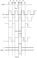
- the corresponding input/output timing diagram is as shown in Fig.4a . In particular, five phases S1, S2, S3, S4 and S5 in the input/output timing diagram as shown in Fig.4a are selected.
- both the second switch transistor T2 and the sixth switch transistor T6 are turned off. Since the eighth transistor T8 is turned on, the potential of the first direct current signal V1 is provided to the third node C, and thus the potential of the third node C is the low potential. Since the potential of the third node C is the low potential, the tenth switch transistor T10 is turned off. Since the ninth switch transistor T9 is turned on and provides the second direct current signal V2 to the driving signal output terminal Output, the driving signal output terminal Output outputs the scanning signal with the high potential.
- the first clock signal CK with the low potential is provided to the first node A through the second switch transistor T2 and the third switch transistor T3, and thus the potential of the first node A is the low potential. Since the potential of the first node A is the low potential, the fourth switch transistor T4, the eighth switch transistor T8 and the ninth switch transistor T9 are turned off. Since both the sixth switch transistor T6 and the seventh transistor T7 are turned on and provide the second direct current signal V2 to the third node C through the sixth switch transistor T6 and the seventh transistor T7, the potential of the third node C is the high potential, and thus the third capacitor C3 starts to be charged.
- the tenth switch transistor T10 Since the potential of the third node C is the high potential, the tenth switch transistor T10 is turned on. Since the tenth switch transistor T10 is turned on and provides the first direct current signal V1 to the driving signal output terminal Output, the driving signal output terminal Output outputs the scanning signal with the low potential.
- the shift register provided in the embodiment of the present disclosure keeps repeating execution of phases S2 and S1 until the next frame starts.
- the operation process of the shift register is described by taking the structure of the shift register as shown in Fig.2b as an example.
- the time length of the valid pulse signal of the input signal Input is prolonged one clock signal cycle, and its corresponding input/output timing diagram is as shown in Fig.4b .
- five phases S1, S2, S3, S4, and S5 in the input/output timing diagram as shown in Fig.4b are selected, wherein phase S3 is divided into three phases S31, S32, and S33.
- the specific operation process is the same as the operation process in phase S1 in embodiment 1. Thus, no further description is given herein.
- the specific operation process is the same as the operation process in phase S2 in Embodiment 4. Thus, no further description is given herein.
- the first clock signal CK with the low potential is provided to the first node A through the second switch transistor T2 and the third switch transistor T3, and thus the potential of the first node A is the low potential. Since the potential of the first node A is the low potential, the fourth switch transistor T4, the eighth switch transistor T8 and the ninth switch transistor T9 are turned off. Since the sixth switch transistor T6 and the seventh switch transistor T7 are turned on and the second direct current signal V2 is provided to the third node C through the sixth switch transistor T6 and the seventh switch transistor T7, the potential of the third node C is the high potential, and the third capacitor C3 starts to be charged.
- the tenth switch transistor T10 Since the potential of the third node C is the high potential, the tenth switch transistor T10 is turned on. Since the tenth switch transistor T10 is turned on and provides the first direct current signal V1 to the driving signal output terminal Output, the driving signal output terminal Output outputs the scanning signal with the low potential.
- the potential of the third node C is the high potential. Since the potential of the third node C is the high potential, the tenth switch transistor T10 is turned on. Since the tenth switch transistor T10 is turned on and provides the first direct current signal V1 to the driving signal output terminal Output, the driving signal output terminal Output outputs the scanning signal with the low potential.
- the specific operation process is the same as the operation process in phase S4 in Embodiment 4. Thus, no further description is given herein.
- the specific operation process is the same as the operation process in phase S5 in Embodiment 4. Thus, no further description is given herein.
- the shift register provided in the embodiment of the present disclosure keeps repeating execution of phases S2 and S1 until the next frame starts.
- the operation process of the shift register is described by taking the structure of the shift register as shown in Fig.2b as an example.
- the time length of the valid pulse signal of the input signal Input is prolonged one clock signal cycle, and its corresponding input/output timing diagram is as shown in Fig.4c .
- five phases S1, S2, S3, S4, and S5 in the input/output timing diagram as shown in Fig.4c are selected, wherein phase S3 is divided into is divided into five phases S31, S32, S33, S34, and S35.
- the specific operation process is the same as the operation process in phase S1 in Embodiment 4. Thus, no further description is given herein.
- the specific operation process is the same as the operation process in phase S2 in Embodiment 4. Thus, no further description is given herein.
- the specific operation process is the same as the operation process in phase S31 in Embodiment 4. Thus, no further description is given herein.
- the specific operation process is the same as the operation process in phase S32 in Embodiment 4. Thus, no further description is given herein.
- the first clock signal CK with the low potential is provided to the first node A through the second switch transistor T2 and the third switch transistor T3, and thus the potential of the first node A is the low potential. Since the potential of the first node A is the low potential, the fourth switch transistor T4, the eighth switch transistor T8 and the ninth switch transistor T9 are turned off. Since the sixth switch transistor T6 and the seventh switch transistor T7 are turned on, and the second direct current signal V2 is provided to the third node C through the sixth switch transistor T6 and the seventh switch transistor T7, the potential of the third node C is the high potential, and thus the third capacitor C3 starts to be charged.
- the tenth switch transistor T10 Since the potential of the third node C is the high potential, the tenth switch transistor T10 is turned on. Since the tenth switch transistor T10 is turned on and provides the first direct current signal V1 to the driving signal output terminal Output, the driving signal output terminal outputs the scanning signal with the low potential. It can be seen that the operation process of phase S33 is the same as the operation process of phase S32. It can be seen that the operation process of phase S34 is the same as the operation process of phase S32.
- phase S35 is the same as the operation process of phase S33 in Embodiment 5.
- the specific operation process is the same as the operation process of phase S4 in Embodiment 4. Thus, no further description is given herein.
- the specific operation process is the same as the operation process of phase S5 in Embodiment 4. Thus, no further description is given herein.
- phase S5 the shift register provided in the embodiment of the present disclosure keeps repeating execution of phases S2 and S1 until the next frame starts.
- Embodiment 4 Embodiment 5 and Embodiment 6 that, on the basis of the input signal in Embodiment 4, the shift register provided in the embodiment of the present disclosure can output the scanning signal with a corresponding time length in Embodiment 5 by prolonging one clock signal cycle of the time length of the valid pulse signal of the input signal, and can output the scanning signal with a corresponding time length in Embodiment 6 by prolonging two clock signal cycles of the time length of the valid pulse signal of the input signal, and so forth.
- the scanning signal having the same time length as the valid pulse signal of the input signal can be realized.
- the above shift registers need to control the time length of the scanning signal outputted by the driving signal output terminal by just changing the time length of the input signal, without changing the clock signal and changing the circuit and the manufacturing process. Therefore, compared with controlling the time length of the scanning signal outputted by the driving signal output terminal by using a variety of clock control signals in the prior art, the shift registers in the present disclosure could reduce difficulty of the gate driving circuit and reduce process complexity, thereby reducing the cost.
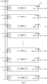
- a gate driving circuit as shown in Fig.5 , comprising multiple shift registers connected in series: SR(1), SR(2) ... SR(n) ... SR(N-1), SR(N) (totally N shift registers, 1 ⁇ n ⁇ N), wherein an input signal Input of a first stage of shift register SR(1) is inputted by a start signal terminal STV. Except for the first stage of shift register SR(1), input signals Input of remaining respective stages of shift registers SR(n)are inputted by a driving signal output terminal Output_n-1 of a previous stage of shift register SR(n-1) connected thereto.
- a first clock signal CK, a second clock signal CB, a first direct current signal V1 and a second direct current signal V2 are inputted into the respective stages of shift registers.
- each shift register in the gate driving circuit has the same function and structure as the above shift register in the embodiments of the present disclosure, and thus no further description is given herein.
- the gate driving circuit could be applied to a liquid crystal display panel LCD, or could be applied to an organic light-emitting display panel, to which no further limitation is made.
- the scanning time length of the gate driving circuit adopted is fixed, and pixels of respective rows in the display panel are in a light-emitting state after scanning starts, thereby resulting in that it is not easy to adjust the light-emitting time of pixels of respective rows in the display panel.
- the gate driving circuit provided in the present disclosure needs to control the time length of the scanning signal outputted by the driving signal output terminal by just changing the time length of the input signal. Therefore, application of the gate driving circuit provided in the embodiments of the present disclosure into the OLED display panel can control the time length of the scanning signal by changing the time length of the input signal, so that the light-emitting time of pixels of respective rows is controlled by controlling the scanning time, and thus the light-emitting luminance of the OLED display panel could be controlled.
- an organic light-emitting display panel comprising the gate driving circuit described above. Scanning signals are provided for respective gate lines on the array substrate in the organic light-emitting display panel through the this gate driving circuit, please referring to the above description above the gate driving circuit for the specific implementation, and thus no further description is given herein.
- a display device comprising the organic light-emitting display panel provided in the embodiment of the present disclosure.
- the shift register, the gate driving circuit and the relevant display device comprise: the first node controlling module, the second node controlling module, the third node controlling module, the first outputting module, and the second outputting module, wherein the first node controlling module adjusts the potential of the first node through the input signal, the first clock signal, the second clock signal, the first direct current signal and the potential of the second node, the second node controlling module adjusts the potential of the second node through the first clock signal, the second clock signal, the first direct current signal, the second direct current signal and the potential of the first node, the third node controlling module adjusts the potential of the third node through the second clock signal, the second direct current signal, the potential of the first node and the potential of the second node, the first outputting module adjusts the potential of the driving signal output terminal through the second direct current signal and the potential of the first node, and the second outputting module adjusts the potential of the driving signal output terminal though the first direct current signal and the potential of the third node.
- the shift register could control the time length of the scanning signal outputted by the driving signal output terminal by only changing the time length of the input signal, without changing the clock signal, changing the circuit and changing the process. Therefore, compared with the prior art where the time length of the scanning signal outputted by the driving signal output terminal is controlled by using various clock control signals, the present disclosure could reduce difficulty of the gate driving circuit and solve problem of process complexity, so as to reduce cost.
Landscapes
- Engineering & Computer Science (AREA)
- Physics & Mathematics (AREA)
- Computer Hardware Design (AREA)
- General Physics & Mathematics (AREA)
- Theoretical Computer Science (AREA)
- Chemical & Material Sciences (AREA)
- Crystallography & Structural Chemistry (AREA)
- Control Of Indicators Other Than Cathode Ray Tubes (AREA)
- Shift Register Type Memory (AREA)
- Liquid Crystal Display Device Control (AREA)
Claims (7)
- Schieberegister mit:einem ersten Knotenkontrollmodul (1) mit einem ersten bis fünften Eingabeanschluss und einem Ausgabeanschluss, wobei der erste Eingabeanschluss verbunden ist mit einem Eingabesignal (Input), der zweite Eingabeanschluss verbunden ist mit einem ersten Taktsignal (CK), der dritte Eingabeanschluss verbunden ist mit einem zweiten Taktsignal (CB), der vierte Eingabeanschluss verbunden ist mit einem ersten Gleichstromsignal (V1), der fünfte Eingabeanschluss verbunden ist mit einem zweiten Knoten (B) und der Ausgabeanschluss verbunden ist mit einem ersten Knoten (A) und wobei das erste Knotenkontrollmodul (1) konfiguriert ist, das Eingabesignal an dem ersten Knoten (A) bereitzustellen, wenn ein Potential des ersten Taktsignals (CK) ein erstes Potential ist, und das zweite Gleichstromsignal (V1) an dem ersten Knoten (A) bereitzustellen, wenn sowohl ein Potential des zweiten Taktsignals (V2) und ein Potential des zweiten Knotens (B) das erste Potential sind;ein zweites Knotenkontrollmodul (2) aufweist einen ersten bis vierten Eingabeanschluss und einen Ausgabeanschluss, wobei der erste Eingabeanschluss verbunden ist mit einem zweiten Gleichstromsignal (V2), der zweite Eingabeanschluss verbunden ist mit dem ersten Taktsignal (CK), der dritte Eingabeanschluss verbunden ist mit dem zweiten Taktsignal (CB), der vierte Eingabeanschluss verbunden ist mit dem ersten Knoten (A) und der Ausgabeanschluss verbunden ist mit dem zweiten Knoten (B), und wobei das zweite Knotensteuermodul (2) konfiguriert ist, das zweite Gleichstromsignal (V2) an dem zweiten Knoten (B) bereitzustellen, wenn ein Potential des ersten Taktsignals (CK) das erste Potential ist und das erste Taktsignal (CK) an dem zweiten Knoten (B) bereitzustellen, wenn ein Potential des ersten Knotens (A) das erste Potential ist;ein drittes Knotensteuermodul (3) mit einem ersten bis fünften Eingabeanschluss und einem Ausgabeanschluss, wobei der erste Eingabeanschluss verbunden ist mit dem zweiten Taktsignal (CB), der zweite Eingabeanschluss verbunden ist mit dem ersten Gleichstromsignal (V1), der dritte Eingabeanschluss verbunden ist mit dem zweiten Gleichstromsignal (V2), der vierte Eingabeanschluss verbunden ist mit dem ersten Knoten (A), der fünfte Eingabeanschluss verbunden ist mit dem zweiten Knoten (B) und der Ausgabeanschluss verbunden ist mit dem dritten Knoten (C), und wobei das dritte Knotensteuermodul (3) konfiguriert ist, das erste Gleichstromsignal (V1) an dem dritten Knoten (C) bereitzustellen, wenn das Potential des ersten Knotens (A) das erste Potential ist, und das zweite Gleichstromsignal (V2) an dem dritten Knoten (C) bereitzustellen, wenn sowohl das Potential des zweiten Taktsignals (CB) als auch das Potential des zweiten Knotens (B) das erste Potential sind;ein erstes Ausgabemodul (4) mit einem ersten und zweiten Eingabeanschluss und einem Ausgabeanschluss, wobei der erste Eingabeanschluss verbunden ist mit dem zweiten Gleichstromsignal (V2), der zweite Eingabeanschluss verbunden ist mit dem ersten Knoten (A) und der Ausgabeanschluss verbunden ist mit einem Steuersignalausgabeanschluss (Output) des Schieberegisters, und wobei das erste Ausgabemodul (4) konfiguriert ist, das zweite Gleichstromsignal (V2) an dem Steuersignalausgabeanschluss (Output) bereitzustellen, wenn das Potential des ersten Knotens (A) das erste Potential ist;ein zweites Ausgabemodul (5) mit einem ersten und einem zweiten Eingabeanschluss und einem Ausgabeanschluss, wobei der erste Eingabeanschluss verbunden ist mit dem ersten Gleichstromsignal (V1), der zweite Eingabeanschluss verbunden ist mit dem dritten Knoten (C) und der Ausgabeanschluss verbunden ist mit dem Steuersignalausgabeanschluss (Output), und wobei das zweite Ausgabemodul (5) konfiguriert ist, das erste Gleichstromsignal (V1) an dem Steuersignalausgabeanschluss (Output) bereitzustellen, wenn das Potential des dritten Knotens (C) das erste Potential ist,dadurch gekennzeichnet, dassdas erste Knotensteuermodul (1) aufweist: einen ersten Schalttransistor (T1), einen zweiten Schalttransistor (T2), einen dritten Schalttransistor (T3), und einen ersten Kondensator (C1); wobei,ein Gate des ersten Schalttransistors (T1) verbunden ist mit dem ersten Taktsignal (CK), seine Source verbunden ist mit dem Eingabesignal (Input) und sein Drain verbunden ist mit dem ersten Knoten (A);ein Gate des zweiten Schalttransistors (T2) verbunden ist mit dem zweiten Knoten (B), seine Source verbunden ist mit dem ersten Gleichstromsignal (V1) und sein Drain verbunden ist mit einer Source des dritten Schalttransistors (T3);ein Gate des dritten Schalttransistors (T3) verbunden ist mit dem zweiten Taktsignal (CB) und sein Drain verbunden ist mit dem ersten Knoten (A); undein Anschluss des ersten Kondensators (C1) verbunden ist mit dem ersten Knoten (A) und sein anderer Anschluss verwendet wird, um das zweite Taktsignal (CB) zu empfangen;das zweite Knotensteuermodul (2) aufweist: einen vierten Schalttransistor (T4), einen fünften Schalttransistor (T5) und einen zweiten Kondensator (C2); wobeiein Gate des vierten Schalttransistors (T4) verbunden ist mit dem ersten Knoten (A), seine Source verbunden ist mit dem ersten Taktsignal (CK) und sein Drain verbunden ist mit dem zweiten Knoten (B);ein Gate des fünften Schalttransistors (T5) verbunden ist mit dem ersten Taktsignal (CK), seine Source verbunden ist mit dem zweiten Gleichstromsignal (V2) und sein Drain verbunden ist mit dem zweiten Knoten (B); undein Anschluss des zweiten Kondensators (C2) verbunden ist mit dem zweiten Knoten (B) und sein anderer Anschluss verbunden ist mit dem zweiten Taktsignal (CB);das dritte Knotensteuermodul (3) aufweist: einen sechsten Schalttransistor (T6), einen siebten Schalttransistor (T7), einen achten Schalttransistor (T8), und einen dritten Kondensator (C3); wobei,ein Gate des sechsten Schalttransistors (T6) verbunden ist mit dem zweiten Knoten (B), seine Source verbunden ist mit dem zweiten Gleichstromsignal (V2) und sein Drain verbunden ist mit einer Source des siebten Schalttransistors (T7);ein Gate des siebten Schalttransistors (T7) verbunden ist mit dem zweiten Taktsignal (CB); und sein Drain verbunden ist mit dem dritten Knoten (C);ein Gate des achten Schalttransistors (T8) verbunden ist mit ersten Knoten (A), seine Source verbunden ist mit dem ersten Gleichstromsignal (V1) und sein Drain verbunden ist mit dem dritten Knoten (C); undein Anschluss des dritten Kondensators (C3) verbunden ist mit dem dritten Knoten (C) und sein anderer Anschluss verbunden ist mit dem ersten Gleichstromsignal (V1);das erste Ausgabemodul (4) aufweist: einen neunten Schalttransistor (T9); wobei,ein Gate des neunten Schalttransistors (T) verbunden ist mit dem ersten Knoten (A), seine Source verbunden ist mit dem zweiten Gleichstromsignal, und sein Drain verbunden ist mit dem Ansteuersignalausgabeanschluss (Output); unddas zweite Ausgabemodul (5) aufweist einen zehnten Schalttransistor (T10); wobei,ein Gate des zehnten Schalttransistors (T10) verbunden ist mit dem dritten Knoten (C), seine Source verbunden ist mit dem ersten Gleichstromsignal (V1) und sein Drain verbunden ist mit dem Ansteuersignalausgabeanschluss (Output).
- Schieberegister gemäß Anspruch 1, wobei das Schieberegister derart konfiguriert ist, dass
sobald ein gültiges Puls-Signal des Eingabesignals (Input) ein High-Potential ist, das erste Potential ein Low-Potential ist, und sobald ein Potential des ersten Gleichstromsignals (V1) ein High-Potential ist, ein Potential des zweiten Gleichstromsignals (V2) ein Low-Potential ist; oder
sobald das gültige Puls-Signal des Eingabesignals (Input) ein Low-Potential ist, das erste Potential ein High-Potential ist, und sobald ein Potential des ersten Gleichstromsignals (V1) ein Low-Potential ist, ein Potential des zweiten Gleichstromsignals (V2) ein High-Potential ist. - Schieberegister gemäß einem der Ansprüche 1 bis 2, wobei das Schieberegister derart konfiguriert ist, dass
wenn das gültige Puls-Signal des Eingabesignals (Input) ein High-Potential ist, alle Schalttransistoren P-Typ-Transistoren sind; sobald ein gültiges Puls-Signal des Eingabesignals (Input) ein Low-Potential ist, alle Schalttransistoren N-Typ-Transistoren sind. - Schieberegister gemäß Anspruch 3, wobei das Schieberegister derart konfiguriert ist, dass
wenn das gültige Puls-Signal des Eingabesignals (Input) ein High-Potential ist, eine ansteigende Flanke des Eingabesignals (Input) mit einer fallenden Kante des ersten Taktsignals (CK) und einer steigenden Flanke des zweiten Taktsignals (CB) übereinstimmt, und eine fallende Flanke des Eingangssignals (Input) mit einer steigenden Flanke des ersten Taktsignals (CK) übereinstimmt; wobei das erste Taktsignal (CK) und das zweite Taktsignal (CB) einen gleichen Zyklus und ein gleiches Tastverhältnis haben und das Tastverhältnis größer als 0,5 ist; oder
sobald das gültige Puls-Signal des Eingangssignals (Input) ein Low-Potential ist, die fallende Flanke des Eingangssignals (Input) mit der steigenden Flanke des ersten Taktsignals (CK) und der fallenden Flanke des zweiten Taktsignals (CB) übereinstimmt und die steigende Flanke des Eingangssignals (Input) mit der fallenden Flanke des ersten Taktsignals (CK) übereinstimmt, wobei das erste Taktsignal (CK) und das zweite Taktsignal (CB) einen gleichen Zyklus und ein gleiches Tastverhältnis haben und das Tastverhältnis kleiner als 0,5 ist. - Gate-Ansteuerschaltung mit mehreren Schieberegistern gemäß einem der Ansprüche 1 bis 4, die in Serie verschaltet sind, wobei die Gate-Ansteuerschaltung derart konfiguriert ist,
dass ein Eingabesignal (Input) einer ersten Stufe von Schieberegistern von einem Startsignalanschluss eingegeben wird;
dass, mit Ausnahme für die erste Stufe von Schieberegistern, Eingabesignale (Input) der verbleibenden Stufen der Schieberegister von einem Ansteuersignalausgabeanschluss (Output) einer vorhergehenden Stufe des damit verbundenen Schieberegisters eingegeben werden. - Organisches lichtaussendendes Anzeigepanel mit der Gate-Ansteuerschaltung gemäß Anspruch 5.
- Anzeigevorrichtung mit dem organischen lichtaussendenden Anzeigepanel gemäß Anspruch 6.
Applications Claiming Priority (2)
| Application Number | Priority Date | Filing Date | Title |
|---|---|---|---|
| CN201510536801.4A CN105185287B (zh) | 2015-08-27 | 2015-08-27 | 一种移位寄存器、栅极驱动电路和相关显示装置 |
| PCT/CN2016/073624 WO2017031955A1 (zh) | 2015-08-27 | 2016-02-05 | 移位寄存器、栅极驱动电路和相关显示装置 |
Publications (3)
| Publication Number | Publication Date |
|---|---|
| EP3343565A1 EP3343565A1 (de) | 2018-07-04 |
| EP3343565A4 EP3343565A4 (de) | 2019-01-09 |
| EP3343565B1 true EP3343565B1 (de) | 2020-04-01 |
Family
ID=54907322
Family Applications (1)
| Application Number | Title | Priority Date | Filing Date |
|---|---|---|---|
| EP16808897.9A Active EP3343565B1 (de) | 2015-08-27 | 2016-02-05 | Schieberegister, gatetreiberschaltung und zugehörige anzeigevorrichtung |
Country Status (4)
| Country | Link |
|---|---|
| US (1) | US9799272B2 (de) |
| EP (1) | EP3343565B1 (de) |
| CN (1) | CN105185287B (de) |
| WO (1) | WO2017031955A1 (de) |
Families Citing this family (30)
| Publication number | Priority date | Publication date | Assignee | Title |
|---|---|---|---|---|
| CN104952396B (zh) * | 2015-06-30 | 2017-10-31 | 上海天马有机发光显示技术有限公司 | 一种移位寄存器及其驱动方法 |
| CN105185287B (zh) * | 2015-08-27 | 2017-10-31 | 京东方科技集团股份有限公司 | 一种移位寄存器、栅极驱动电路和相关显示装置 |
| CN105047124B (zh) * | 2015-09-18 | 2017-11-17 | 京东方科技集团股份有限公司 | 一种移位寄存器、栅极驱动电路及显示装置 |
| CN105118418B (zh) * | 2015-09-25 | 2017-08-11 | 京东方科技集团股份有限公司 | 一种移位寄存器、其驱动方法、栅极驱动电路及显示装置 |
| CN105118417B (zh) * | 2015-09-25 | 2017-07-25 | 京东方科技集团股份有限公司 | 一种移位寄存器、其驱动方法、栅极驱动电路及显示装置 |
| CN105304057B (zh) * | 2015-12-09 | 2018-11-30 | 京东方科技集团股份有限公司 | 一种移位寄存器及其驱动方法、栅极驱动电路 |
| CN105679248B (zh) | 2016-01-04 | 2017-12-08 | 京东方科技集团股份有限公司 | 移位寄存器单元及其驱动方法、栅极驱动电路、显示装置 |
| CN105632444B (zh) * | 2016-03-16 | 2017-12-26 | 京东方科技集团股份有限公司 | 一种移位寄存器、栅极驱动电路及显示面板 |
| CN106251818A (zh) * | 2016-08-31 | 2016-12-21 | 深圳市华星光电技术有限公司 | 一种栅极驱动电路 |
| US10395600B2 (en) * | 2016-10-19 | 2019-08-27 | Apple Inc. | Integrated gate driver circuit |
| KR102721846B1 (ko) * | 2016-11-30 | 2024-10-24 | 엘지디스플레이 주식회사 | 표시 장치용 발광 제어부 및 이를 적용한 유기 발광 표시 장치 |
| CN106652882B (zh) * | 2017-03-17 | 2019-09-06 | 京东方科技集团股份有限公司 | 移位寄存器单元、阵列基板和显示装置 |
| CN106887209B (zh) * | 2017-04-28 | 2019-04-16 | 京东方科技集团股份有限公司 | 移位寄存器单元及其驱动方法、移位寄存器以及显示装置 |
| CN107358914B (zh) * | 2017-07-12 | 2019-08-06 | 上海天马有机发光显示技术有限公司 | 一种发光控制电路、其驱动方法、显示面板及显示装置 |
| CN107154234B (zh) * | 2017-07-20 | 2020-01-21 | 京东方科技集团股份有限公司 | 移位寄存器单元、驱动方法、栅极驱动电路和显示装置 |
| CN107657918B (zh) * | 2017-09-29 | 2019-10-01 | 上海天马微电子有限公司 | 发光控制信号生成电路、其驱动方法及装置 |
| CN107633834B (zh) * | 2017-10-27 | 2020-03-31 | 京东方科技集团股份有限公司 | 移位寄存单元、其驱动方法、栅极驱动电路及显示装置 |
| CN109616056A (zh) | 2018-08-24 | 2019-04-12 | 京东方科技集团股份有限公司 | 移位寄存器及其驱动方法、栅极驱动电路和显示装置 |
| CN108877662B (zh) * | 2018-09-13 | 2020-03-31 | 合肥鑫晟光电科技有限公司 | 栅极驱动电路及其控制方法、显示装置 |
| KR102750942B1 (ko) * | 2018-10-30 | 2025-01-08 | 엘지디스플레이 주식회사 | 게이트 드라이버와 이를 포함한 유기발광 표시장치 |
| KR102668648B1 (ko) * | 2018-12-14 | 2024-05-24 | 삼성디스플레이 주식회사 | 표시 장치 |
| US11308854B2 (en) | 2019-03-22 | 2022-04-19 | Boe Technology Group Co., Ltd. | Shift register unit, driving circuit, display device and driving method |
| CN111091791B (zh) * | 2019-11-15 | 2021-08-24 | 京东方科技集团股份有限公司 | 移位寄存器及其驱动方法、栅极驱动电路 |
| TWI728783B (zh) * | 2020-04-21 | 2021-05-21 | 友達光電股份有限公司 | 顯示裝置 |
| CN111429830B (zh) * | 2020-04-23 | 2022-09-09 | 合肥京东方卓印科技有限公司 | 移位寄存器单元及其驱动方法、栅极驱动电路、显示面板 |
| CN113554986A (zh) * | 2020-04-26 | 2021-10-26 | 华为技术有限公司 | 移位寄存器及驱动方法、发光控制电路、阵列基板及终端 |
| CN114097020B (zh) * | 2020-04-30 | 2024-03-15 | 京东方科技集团股份有限公司 | 移位寄存器、栅极驱动电路和栅极驱动方法 |
| CN112509533A (zh) * | 2020-12-14 | 2021-03-16 | 福建华佳彩有限公司 | 一种新型的gip电路及其驱动方法 |
| CN112967654B (zh) * | 2021-03-23 | 2024-04-05 | 福建华佳彩有限公司 | 一种gip电路及驱动方法 |
| CN119107890B (zh) * | 2024-10-10 | 2025-11-14 | 武汉天马微电子有限公司上海分公司 | 一种显示面板及显示装置 |
Family Cites Families (14)
| Publication number | Priority date | Publication date | Assignee | Title |
|---|---|---|---|---|
| TW538400B (en) * | 1999-11-01 | 2003-06-21 | Sharp Kk | Shift register and image display device |
| US7050036B2 (en) * | 2001-12-12 | 2006-05-23 | Lg.Philips Lcd Co., Ltd. | Shift register with a built in level shifter |
| KR100583318B1 (ko) * | 2003-12-17 | 2006-05-25 | 엘지.필립스 엘시디 주식회사 | 액정표시장치의 게이트 구동장치 및 방법 |
| KR101082909B1 (ko) * | 2005-02-05 | 2011-11-11 | 삼성전자주식회사 | 게이트 구동 방법 및 그 장치와 이를 갖는 표시장치 |
| KR101447997B1 (ko) * | 2008-04-14 | 2014-10-08 | 삼성디스플레이 주식회사 | 표시 장치 및 그 구동 방법 |
| CN102708779B (zh) * | 2012-01-13 | 2014-05-14 | 京东方科技集团股份有限公司 | 移位寄存器及其驱动方法、栅极驱动装置与显示装置 |
| CN102629463B (zh) * | 2012-03-29 | 2013-10-09 | 京东方科技集团股份有限公司 | 移位寄存器单元、移位寄存器电路、阵列基板及显示器件 |
| KR101510583B1 (ko) * | 2014-01-16 | 2015-04-08 | 경희대학교 산학협력단 | 가변 펄스폭 쉬프트 레지스터 |
| CN104134430B (zh) * | 2014-07-04 | 2016-08-17 | 京东方科技集团股份有限公司 | 一种移位寄存器、栅极驱动电路及显示装置 |
| CN104537979B (zh) * | 2015-01-28 | 2017-03-15 | 京东方科技集团股份有限公司 | 移位寄存器及其驱动方法、栅极驱动电路 |
| CN104835531B (zh) * | 2015-05-21 | 2018-06-15 | 京东方科技集团股份有限公司 | 一种移位寄存器单元及其驱动方法、移位寄存器和显示装置 |
| CN104809978B (zh) * | 2015-05-21 | 2017-05-17 | 京东方科技集团股份有限公司 | 移位寄存器单元、驱动方法、栅极驱动电路及显示装置 |
| CN104835450B (zh) * | 2015-05-22 | 2017-01-25 | 京东方科技集团股份有限公司 | 移位寄存器单元及其控制方法、栅极驱动电路、显示装置 |
| CN105185287B (zh) * | 2015-08-27 | 2017-10-31 | 京东方科技集团股份有限公司 | 一种移位寄存器、栅极驱动电路和相关显示装置 |
-
2015
- 2015-08-27 CN CN201510536801.4A patent/CN105185287B/zh active Active
-
2016
- 2016-02-05 WO PCT/CN2016/073624 patent/WO2017031955A1/zh not_active Ceased
- 2016-02-05 EP EP16808897.9A patent/EP3343565B1/de active Active
- 2016-02-05 US US15/320,613 patent/US9799272B2/en active Active
Non-Patent Citations (1)
| Title |
|---|
| None * |
Also Published As
| Publication number | Publication date |
|---|---|
| EP3343565A1 (de) | 2018-07-04 |
| US20170200418A1 (en) | 2017-07-13 |
| EP3343565A4 (de) | 2019-01-09 |
| WO2017031955A1 (zh) | 2017-03-02 |
| CN105185287B (zh) | 2017-10-31 |
| US9799272B2 (en) | 2017-10-24 |
| CN105185287A (zh) | 2015-12-23 |
Similar Documents
| Publication | Publication Date | Title |
|---|---|---|
| EP3343565B1 (de) | Schieberegister, gatetreiberschaltung und zugehörige anzeigevorrichtung | |
| EP3355309B1 (de) | Schieberegister, gatetreiberschaltung und anzeigevorrichtung | |
| CN111477181B (zh) | 栅极驱动电路、显示基板、显示装置和栅极驱动方法 | |
| CN105118417B (zh) | 一种移位寄存器、其驱动方法、栅极驱动电路及显示装置 | |
| EP3333843B1 (de) | Schieberegister, gatetreiberschaltung, ansteuerungsverfahren für anzeigetafel sowie anzeigevorrichtung | |
| US10580376B2 (en) | Shift register and driving method thereof, gate driving circuit and display apparatus | |
| CN105427825B (zh) | 一种移位寄存器、其驱动方法及栅极驱动电路 | |
| EP3214616B1 (de) | Goa-einheit und ansteuerungsverfahren, goa-schaltung und anzeigevorrichtung | |
| CN105118418B (zh) | 一种移位寄存器、其驱动方法、栅极驱动电路及显示装置 | |
| CN104978943B (zh) | 一种移位寄存器、显示面板的驱动方法及相关装置 | |
| CN105788508B (zh) | 一种栅极驱动电路及显示面板 | |
| CN105741744B (zh) | 一种移位寄存器单元、栅极驱动电路及显示装置 | |
| EP3709287B1 (de) | Gatetreiberschaltung und ansteuerungsverfahren dafür und anzeigevorrichtung | |
| EP3306602A1 (de) | Schieberegister, ansteuerungsschaltung für gate-elektrode und anzeigevorrichtung | |
| CN105304057A (zh) | 一种移位寄存器及其驱动方法、栅极驱动电路 | |
| CN104299590A (zh) | 一种移位寄存器、其驱动方法、栅极驱动电路及显示装置 | |
| CN104134430A (zh) | 一种移位寄存器、栅极驱动电路及显示装置 | |
| US10467966B2 (en) | Shift register and a method for driving the same, a gate driving circuit and display apparatus | |
| GB2547577A (en) | Liquid crystal display device and gate driver thereof | |
| CN107610736A (zh) | 一种移位寄存器、栅极驱动电路及显示装置 | |
| CN105632563A (zh) | 一种移位寄存器、栅极驱动电路及显示装置 | |
| CN104934071A (zh) | 一种移位寄存器、栅极驱动电路及显示装置 | |
| CN104217764A (zh) | 移位寄存器、其驱动方法、栅极驱动电路及显示装置 | |
| EP3226231B1 (de) | Gate-treiberschaltung und anzeigevorrichtung | |
| CN107516492A (zh) | 一种移位寄存器、栅极驱动电路及显示装置 |
Legal Events
| Date | Code | Title | Description |
|---|---|---|---|
| STAA | Information on the status of an ep patent application or granted ep patent |
Free format text: STATUS: UNKNOWN |
|
| STAA | Information on the status of an ep patent application or granted ep patent |
Free format text: STATUS: THE INTERNATIONAL PUBLICATION HAS BEEN MADE |
|
| PUAI | Public reference made under article 153(3) epc to a published international application that has entered the european phase |
Free format text: ORIGINAL CODE: 0009012 |
|
| STAA | Information on the status of an ep patent application or granted ep patent |
Free format text: STATUS: REQUEST FOR EXAMINATION WAS MADE |
|
| 17P | Request for examination filed |
Effective date: 20161219 |
|
| AK | Designated contracting states |
Kind code of ref document: A1 Designated state(s): AL AT BE BG CH CY CZ DE DK EE ES FI FR GB GR HR HU IE IS IT LI LT LU LV MC MK MT NL NO PL PT RO RS SE SI SK SM TR |
|
| AX | Request for extension of the european patent |
Extension state: BA ME |
|
| DAV | Request for validation of the european patent (deleted) | ||
| DAX | Request for extension of the european patent (deleted) | ||
| A4 | Supplementary search report drawn up and despatched |
Effective date: 20181211 |
|
| RIC1 | Information provided on ipc code assigned before grant |
Ipc: G09G 3/20 20060101ALI20181205BHEP Ipc: G09G 3/36 20060101ALI20181205BHEP Ipc: G11C 19/28 20060101AFI20181205BHEP Ipc: G09G 3/3266 20160101ALI20181205BHEP |
|
| GRAP | Despatch of communication of intention to grant a patent |
Free format text: ORIGINAL CODE: EPIDOSNIGR1 |
|
| STAA | Information on the status of an ep patent application or granted ep patent |
Free format text: STATUS: GRANT OF PATENT IS INTENDED |
|
| INTG | Intention to grant announced |
Effective date: 20190820 |
|
| GRAS | Grant fee paid |
Free format text: ORIGINAL CODE: EPIDOSNIGR3 |
|
| GRAA | (expected) grant |
Free format text: ORIGINAL CODE: 0009210 |
|
| STAA | Information on the status of an ep patent application or granted ep patent |
Free format text: STATUS: THE PATENT HAS BEEN GRANTED |
|
| AK | Designated contracting states |
Kind code of ref document: B1 Designated state(s): AL AT BE BG CH CY CZ DE DK EE ES FI FR GB GR HR HU IE IS IT LI LT LU LV MC MK MT NL NO PL PT RO RS SE SI SK SM TR |
|
| REG | Reference to a national code |
Ref country code: GB Ref legal event code: FG4D |
|
| REG | Reference to a national code |
Ref country code: AT Ref legal event code: REF Ref document number: 1252419 Country of ref document: AT Kind code of ref document: T Effective date: 20200415 Ref country code: CH Ref legal event code: EP |
|
| REG | Reference to a national code |
Ref country code: DE Ref legal event code: R096 Ref document number: 602016033194 Country of ref document: DE |
|
| REG | Reference to a national code |
Ref country code: IE Ref legal event code: FG4D |
|
| PG25 | Lapsed in a contracting state [announced via postgrant information from national office to epo] |
Ref country code: BG Free format text: LAPSE BECAUSE OF FAILURE TO SUBMIT A TRANSLATION OF THE DESCRIPTION OR TO PAY THE FEE WITHIN THE PRESCRIBED TIME-LIMIT Effective date: 20200701 |
|
| REG | Reference to a national code |
Ref country code: NL Ref legal event code: MP Effective date: 20200401 |
|
| REG | Reference to a national code |
Ref country code: LT Ref legal event code: MG4D |
|
| PG25 | Lapsed in a contracting state [announced via postgrant information from national office to epo] |
Ref country code: NO Free format text: LAPSE BECAUSE OF FAILURE TO SUBMIT A TRANSLATION OF THE DESCRIPTION OR TO PAY THE FEE WITHIN THE PRESCRIBED TIME-LIMIT Effective date: 20200701 Ref country code: GR Free format text: LAPSE BECAUSE OF FAILURE TO SUBMIT A TRANSLATION OF THE DESCRIPTION OR TO PAY THE FEE WITHIN THE PRESCRIBED TIME-LIMIT Effective date: 20200702 Ref country code: LT Free format text: LAPSE BECAUSE OF FAILURE TO SUBMIT A TRANSLATION OF THE DESCRIPTION OR TO PAY THE FEE WITHIN THE PRESCRIBED TIME-LIMIT Effective date: 20200401 Ref country code: NL Free format text: LAPSE BECAUSE OF FAILURE TO SUBMIT A TRANSLATION OF THE DESCRIPTION OR TO PAY THE FEE WITHIN THE PRESCRIBED TIME-LIMIT Effective date: 20200401 Ref country code: SE Free format text: LAPSE BECAUSE OF FAILURE TO SUBMIT A TRANSLATION OF THE DESCRIPTION OR TO PAY THE FEE WITHIN THE PRESCRIBED TIME-LIMIT Effective date: 20200401 Ref country code: PT Free format text: LAPSE BECAUSE OF FAILURE TO SUBMIT A TRANSLATION OF THE DESCRIPTION OR TO PAY THE FEE WITHIN THE PRESCRIBED TIME-LIMIT Effective date: 20200817 Ref country code: FI Free format text: LAPSE BECAUSE OF FAILURE TO SUBMIT A TRANSLATION OF THE DESCRIPTION OR TO PAY THE FEE WITHIN THE PRESCRIBED TIME-LIMIT Effective date: 20200401 Ref country code: CZ Free format text: LAPSE BECAUSE OF FAILURE TO SUBMIT A TRANSLATION OF THE DESCRIPTION OR TO PAY THE FEE WITHIN THE PRESCRIBED TIME-LIMIT Effective date: 20200401 Ref country code: IS Free format text: LAPSE BECAUSE OF FAILURE TO SUBMIT A TRANSLATION OF THE DESCRIPTION OR TO PAY THE FEE WITHIN THE PRESCRIBED TIME-LIMIT Effective date: 20200801 |
|
| REG | Reference to a national code |
Ref country code: AT Ref legal event code: MK05 Ref document number: 1252419 Country of ref document: AT Kind code of ref document: T Effective date: 20200401 |
|
| PG25 | Lapsed in a contracting state [announced via postgrant information from national office to epo] |
Ref country code: LV Free format text: LAPSE BECAUSE OF FAILURE TO SUBMIT A TRANSLATION OF THE DESCRIPTION OR TO PAY THE FEE WITHIN THE PRESCRIBED TIME-LIMIT Effective date: 20200401 Ref country code: HR Free format text: LAPSE BECAUSE OF FAILURE TO SUBMIT A TRANSLATION OF THE DESCRIPTION OR TO PAY THE FEE WITHIN THE PRESCRIBED TIME-LIMIT Effective date: 20200401 Ref country code: RS Free format text: LAPSE BECAUSE OF FAILURE TO SUBMIT A TRANSLATION OF THE DESCRIPTION OR TO PAY THE FEE WITHIN THE PRESCRIBED TIME-LIMIT Effective date: 20200401 |
|
| PG25 | Lapsed in a contracting state [announced via postgrant information from national office to epo] |
Ref country code: AL Free format text: LAPSE BECAUSE OF FAILURE TO SUBMIT A TRANSLATION OF THE DESCRIPTION OR TO PAY THE FEE WITHIN THE PRESCRIBED TIME-LIMIT Effective date: 20200401 |
|
| REG | Reference to a national code |
Ref country code: DE Ref legal event code: R097 Ref document number: 602016033194 Country of ref document: DE |
|
| PG25 | Lapsed in a contracting state [announced via postgrant information from national office to epo] |
Ref country code: RO Free format text: LAPSE BECAUSE OF FAILURE TO SUBMIT A TRANSLATION OF THE DESCRIPTION OR TO PAY THE FEE WITHIN THE PRESCRIBED TIME-LIMIT Effective date: 20200401 Ref country code: IT Free format text: LAPSE BECAUSE OF FAILURE TO SUBMIT A TRANSLATION OF THE DESCRIPTION OR TO PAY THE FEE WITHIN THE PRESCRIBED TIME-LIMIT Effective date: 20200401 Ref country code: EE Free format text: LAPSE BECAUSE OF FAILURE TO SUBMIT A TRANSLATION OF THE DESCRIPTION OR TO PAY THE FEE WITHIN THE PRESCRIBED TIME-LIMIT Effective date: 20200401 Ref country code: SM Free format text: LAPSE BECAUSE OF FAILURE TO SUBMIT A TRANSLATION OF THE DESCRIPTION OR TO PAY THE FEE WITHIN THE PRESCRIBED TIME-LIMIT Effective date: 20200401 Ref country code: DK Free format text: LAPSE BECAUSE OF FAILURE TO SUBMIT A TRANSLATION OF THE DESCRIPTION OR TO PAY THE FEE WITHIN THE PRESCRIBED TIME-LIMIT Effective date: 20200401 Ref country code: ES Free format text: LAPSE BECAUSE OF FAILURE TO SUBMIT A TRANSLATION OF THE DESCRIPTION OR TO PAY THE FEE WITHIN THE PRESCRIBED TIME-LIMIT Effective date: 20200401 Ref country code: AT Free format text: LAPSE BECAUSE OF FAILURE TO SUBMIT A TRANSLATION OF THE DESCRIPTION OR TO PAY THE FEE WITHIN THE PRESCRIBED TIME-LIMIT Effective date: 20200401 |
|
| PLBE | No opposition filed within time limit |
Free format text: ORIGINAL CODE: 0009261 |
|
| STAA | Information on the status of an ep patent application or granted ep patent |
Free format text: STATUS: NO OPPOSITION FILED WITHIN TIME LIMIT |
|
| PG25 | Lapsed in a contracting state [announced via postgrant information from national office to epo] |
Ref country code: PL Free format text: LAPSE BECAUSE OF FAILURE TO SUBMIT A TRANSLATION OF THE DESCRIPTION OR TO PAY THE FEE WITHIN THE PRESCRIBED TIME-LIMIT Effective date: 20200401 Ref country code: SK Free format text: LAPSE BECAUSE OF FAILURE TO SUBMIT A TRANSLATION OF THE DESCRIPTION OR TO PAY THE FEE WITHIN THE PRESCRIBED TIME-LIMIT Effective date: 20200401 |
|
| 26N | No opposition filed |
Effective date: 20210112 |
|
| PG25 | Lapsed in a contracting state [announced via postgrant information from national office to epo] |
Ref country code: SI Free format text: LAPSE BECAUSE OF FAILURE TO SUBMIT A TRANSLATION OF THE DESCRIPTION OR TO PAY THE FEE WITHIN THE PRESCRIBED TIME-LIMIT Effective date: 20200401 |
|
| PG25 | Lapsed in a contracting state [announced via postgrant information from national office to epo] |
Ref country code: MC Free format text: LAPSE BECAUSE OF FAILURE TO SUBMIT A TRANSLATION OF THE DESCRIPTION OR TO PAY THE FEE WITHIN THE PRESCRIBED TIME-LIMIT Effective date: 20200401 |
|
| REG | Reference to a national code |
Ref country code: BE Ref legal event code: MM Effective date: 20210228 |
|
| PG25 | Lapsed in a contracting state [announced via postgrant information from national office to epo] |
Ref country code: LI Free format text: LAPSE BECAUSE OF NON-PAYMENT OF DUE FEES Effective date: 20210228 Ref country code: LU Free format text: LAPSE BECAUSE OF NON-PAYMENT OF DUE FEES Effective date: 20210205 Ref country code: CH Free format text: LAPSE BECAUSE OF NON-PAYMENT OF DUE FEES Effective date: 20210228 |
|
| PG25 | Lapsed in a contracting state [announced via postgrant information from national office to epo] |
Ref country code: IE Free format text: LAPSE BECAUSE OF NON-PAYMENT OF DUE FEES Effective date: 20210205 |
|
| PG25 | Lapsed in a contracting state [announced via postgrant information from national office to epo] |
Ref country code: BE Free format text: LAPSE BECAUSE OF NON-PAYMENT OF DUE FEES Effective date: 20210228 |
|
| PG25 | Lapsed in a contracting state [announced via postgrant information from national office to epo] |
Ref country code: CY Free format text: LAPSE BECAUSE OF FAILURE TO SUBMIT A TRANSLATION OF THE DESCRIPTION OR TO PAY THE FEE WITHIN THE PRESCRIBED TIME-LIMIT Effective date: 20200401 |
|
| PG25 | Lapsed in a contracting state [announced via postgrant information from national office to epo] |
Ref country code: HU Free format text: LAPSE BECAUSE OF FAILURE TO SUBMIT A TRANSLATION OF THE DESCRIPTION OR TO PAY THE FEE WITHIN THE PRESCRIBED TIME-LIMIT; INVALID AB INITIO Effective date: 20160205 |
|
| PG25 | Lapsed in a contracting state [announced via postgrant information from national office to epo] |
Ref country code: MK Free format text: LAPSE BECAUSE OF FAILURE TO SUBMIT A TRANSLATION OF THE DESCRIPTION OR TO PAY THE FEE WITHIN THE PRESCRIBED TIME-LIMIT Effective date: 20200401 |
|
| PG25 | Lapsed in a contracting state [announced via postgrant information from national office to epo] |
Ref country code: TR Free format text: LAPSE BECAUSE OF FAILURE TO SUBMIT A TRANSLATION OF THE DESCRIPTION OR TO PAY THE FEE WITHIN THE PRESCRIBED TIME-LIMIT Effective date: 20200401 |
|
| PG25 | Lapsed in a contracting state [announced via postgrant information from national office to epo] |
Ref country code: MT Free format text: LAPSE BECAUSE OF FAILURE TO SUBMIT A TRANSLATION OF THE DESCRIPTION OR TO PAY THE FEE WITHIN THE PRESCRIBED TIME-LIMIT Effective date: 20200401 |
|
| PGFP | Annual fee paid to national office [announced via postgrant information from national office to epo] |
Ref country code: GB Payment date: 20260219 Year of fee payment: 11 |
|
| PGFP | Annual fee paid to national office [announced via postgrant information from national office to epo] |
Ref country code: DE Payment date: 20260218 Year of fee payment: 11 |
|
| PGFP | Annual fee paid to national office [announced via postgrant information from national office to epo] |
Ref country code: FR Payment date: 20260218 Year of fee payment: 11 |