EP3343603A1 - Structure - Google Patents
Structure Download PDFInfo
- Publication number
- EP3343603A1 EP3343603A1 EP15902264.9A EP15902264A EP3343603A1 EP 3343603 A1 EP3343603 A1 EP 3343603A1 EP 15902264 A EP15902264 A EP 15902264A EP 3343603 A1 EP3343603 A1 EP 3343603A1
- Authority
- EP
- European Patent Office
- Prior art keywords
- region
- heat dissipation
- power semiconductor
- structure according
- fin
- Prior art date
- Legal status (The legal status is an assumption and is not a legal conclusion. Google has not performed a legal analysis and makes no representation as to the accuracy of the status listed.)
- Granted
Links
Images





Classifications
-
- H—ELECTRICITY
- H10—SEMICONDUCTOR DEVICES; ELECTRIC SOLID-STATE DEVICES NOT OTHERWISE PROVIDED FOR
- H10W—GENERIC PACKAGES, INTERCONNECTIONS, CONNECTORS OR OTHER CONSTRUCTIONAL DETAILS OF DEVICES COVERED BY CLASS H10
- H10W40/00—Arrangements for thermal protection or thermal control
- H10W40/20—Arrangements for cooling
- H10W40/22—Arrangements for cooling characterised by their shape, e.g. having conical or cylindrical projections
-
- H—ELECTRICITY
- H10—SEMICONDUCTOR DEVICES; ELECTRIC SOLID-STATE DEVICES NOT OTHERWISE PROVIDED FOR
- H10W—GENERIC PACKAGES, INTERCONNECTIONS, CONNECTORS OR OTHER CONSTRUCTIONAL DETAILS OF DEVICES COVERED BY CLASS H10
- H10W40/00—Arrangements for thermal protection or thermal control
- H10W40/40—Arrangements for thermal protection or thermal control involving heat exchange by flowing fluids
- H10W40/47—Arrangements for thermal protection or thermal control involving heat exchange by flowing fluids by flowing liquids, e.g. forced water cooling
-
- H—ELECTRICITY
- H10—SEMICONDUCTOR DEVICES; ELECTRIC SOLID-STATE DEVICES NOT OTHERWISE PROVIDED FOR
- H10W—GENERIC PACKAGES, INTERCONNECTIONS, CONNECTORS OR OTHER CONSTRUCTIONAL DETAILS OF DEVICES COVERED BY CLASS H10
- H10W40/00—Arrangements for thermal protection or thermal control
- H10W40/70—Fillings or auxiliary members in containers or in encapsulations for thermal protection or control
- H10W40/77—Auxiliary members characterised by their shape
- H10W40/778—Auxiliary members characterised by their shape in encapsulations
-
- H—ELECTRICITY
- H10—SEMICONDUCTOR DEVICES; ELECTRIC SOLID-STATE DEVICES NOT OTHERWISE PROVIDED FOR
- H10W—GENERIC PACKAGES, INTERCONNECTIONS, CONNECTORS OR OTHER CONSTRUCTIONAL DETAILS OF DEVICES COVERED BY CLASS H10
- H10W74/00—Encapsulations, e.g. protective coatings
- H10W74/01—Manufacture or treatment
- H10W74/016—Manufacture or treatment using moulds
-
- H—ELECTRICITY
- H10—SEMICONDUCTOR DEVICES; ELECTRIC SOLID-STATE DEVICES NOT OTHERWISE PROVIDED FOR
- H10W—GENERIC PACKAGES, INTERCONNECTIONS, CONNECTORS OR OTHER CONSTRUCTIONAL DETAILS OF DEVICES COVERED BY CLASS H10
- H10W74/00—Encapsulations, e.g. protective coatings
- H10W74/10—Encapsulations, e.g. protective coatings characterised by their shape or disposition
- H10W74/111—Encapsulations, e.g. protective coatings characterised by their shape or disposition the semiconductor body being completely enclosed
- H10W74/114—Encapsulations, e.g. protective coatings characterised by their shape or disposition the semiconductor body being completely enclosed by a substrate and the encapsulations
-
- H—ELECTRICITY
- H10—SEMICONDUCTOR DEVICES; ELECTRIC SOLID-STATE DEVICES NOT OTHERWISE PROVIDED FOR
- H10W—GENERIC PACKAGES, INTERCONNECTIONS, CONNECTORS OR OTHER CONSTRUCTIONAL DETAILS OF DEVICES COVERED BY CLASS H10
- H10W74/00—Encapsulations, e.g. protective coatings
- H10W74/40—Encapsulations, e.g. protective coatings characterised by their materials
-
- H—ELECTRICITY
- H10—SEMICONDUCTOR DEVICES; ELECTRIC SOLID-STATE DEVICES NOT OTHERWISE PROVIDED FOR
- H10W—GENERIC PACKAGES, INTERCONNECTIONS, CONNECTORS OR OTHER CONSTRUCTIONAL DETAILS OF DEVICES COVERED BY CLASS H10
- H10W76/00—Containers; Fillings or auxiliary members therefor; Seals
- H10W76/10—Containers or parts thereof
- H10W76/12—Containers or parts thereof characterised by their shape
- H10W76/161—Containers comprising no base
-
- H—ELECTRICITY
- H10—SEMICONDUCTOR DEVICES; ELECTRIC SOLID-STATE DEVICES NOT OTHERWISE PROVIDED FOR
- H10W—GENERIC PACKAGES, INTERCONNECTIONS, CONNECTORS OR OTHER CONSTRUCTIONAL DETAILS OF DEVICES COVERED BY CLASS H10
- H10W76/00—Containers; Fillings or auxiliary members therefor; Seals
- H10W76/40—Fillings or auxiliary members in containers, e.g. centering rings
- H10W76/42—Fillings
- H10W76/47—Solid or gel fillings
-
- H—ELECTRICITY
- H10—SEMICONDUCTOR DEVICES; ELECTRIC SOLID-STATE DEVICES NOT OTHERWISE PROVIDED FOR
- H10W—GENERIC PACKAGES, INTERCONNECTIONS, CONNECTORS OR OTHER CONSTRUCTIONAL DETAILS OF DEVICES COVERED BY CLASS H10
- H10W90/00—Package configurations
-
- H—ELECTRICITY
- H10—SEMICONDUCTOR DEVICES; ELECTRIC SOLID-STATE DEVICES NOT OTHERWISE PROVIDED FOR
- H10W—GENERIC PACKAGES, INTERCONNECTIONS, CONNECTORS OR OTHER CONSTRUCTIONAL DETAILS OF DEVICES COVERED BY CLASS H10
- H10W72/00—Interconnections or connectors in packages
- H10W72/071—Connecting or disconnecting
- H10W72/073—Connecting or disconnecting of die-attach connectors
- H10W72/07351—Connecting or disconnecting of die-attach connectors characterised by changes in properties of the die-attach connectors during connecting
-
- H—ELECTRICITY
- H10—SEMICONDUCTOR DEVICES; ELECTRIC SOLID-STATE DEVICES NOT OTHERWISE PROVIDED FOR
- H10W—GENERIC PACKAGES, INTERCONNECTIONS, CONNECTORS OR OTHER CONSTRUCTIONAL DETAILS OF DEVICES COVERED BY CLASS H10
- H10W72/00—Interconnections or connectors in packages
- H10W72/30—Die-attach connectors
-
- H—ELECTRICITY
- H10—SEMICONDUCTOR DEVICES; ELECTRIC SOLID-STATE DEVICES NOT OTHERWISE PROVIDED FOR
- H10W—GENERIC PACKAGES, INTERCONNECTIONS, CONNECTORS OR OTHER CONSTRUCTIONAL DETAILS OF DEVICES COVERED BY CLASS H10
- H10W74/00—Encapsulations, e.g. protective coatings
-
- H—ELECTRICITY
- H10—SEMICONDUCTOR DEVICES; ELECTRIC SOLID-STATE DEVICES NOT OTHERWISE PROVIDED FOR
- H10W—GENERIC PACKAGES, INTERCONNECTIONS, CONNECTORS OR OTHER CONSTRUCTIONAL DETAILS OF DEVICES COVERED BY CLASS H10
- H10W90/00—Package configurations
- H10W90/701—Package configurations characterised by the relative positions of pads or connectors relative to package parts
- H10W90/731—Package configurations characterised by the relative positions of pads or connectors relative to package parts of die-attach connectors
- H10W90/736—Package configurations characterised by the relative positions of pads or connectors relative to package parts of die-attach connectors between a chip and a stacked lead frame, conducting package substrate or heat sink
-
- H—ELECTRICITY
- H10—SEMICONDUCTOR DEVICES; ELECTRIC SOLID-STATE DEVICES NOT OTHERWISE PROVIDED FOR
- H10W—GENERIC PACKAGES, INTERCONNECTIONS, CONNECTORS OR OTHER CONSTRUCTIONAL DETAILS OF DEVICES COVERED BY CLASS H10
- H10W90/00—Package configurations
- H10W90/701—Package configurations characterised by the relative positions of pads or connectors relative to package parts
- H10W90/761—Package configurations characterised by the relative positions of pads or connectors relative to package parts of strap connectors
- H10W90/763—Package configurations characterised by the relative positions of pads or connectors relative to package parts of strap connectors between laterally-adjacent chips
Definitions
- the present invention relates to a structure including a heat dissipation plate, and more particularly to a power semiconductor module mounting a power semiconductor device, and a power conversion device including the power semiconductor module.
- Power conversion devices based on switching of a power semiconductor device are widely used for consumer use, automotive use, railway use, transformer facilities, and the like because of its high conversion efficiency.
- the power semiconductor device generates heat by energization, and thus high heat dissipation is required. Further, the power semiconductor device is sealed with a resin or a gel to secure insulating properties.
- Patent Literature 1 forms a flat heat dissipation surface, and thus the surface area is small and heat exchange efficiency is poor.
- a semiconductor module described in Patent Literature 2 forms a heat dissipation surface having a heat sink exposed on one side. Although heat dissipation to a gas is improved by the heat sink, heat dissipation efficiency is poor due to occurrence of a bypass flow in a case where the semiconductor module is used for cooling in a liquid having superior heat dissipation than gas.
- the present invention is a structure including a heat dissipation plate thermally connected to a heating element, and a resin region having a resin material that fixes the heating element and the heat dissipation plate, wherein the heat dissipation plate includes a fin portion protruding from a heat dissipation surface of the heat dissipation plate, and including a plurality of fins formed to be exposed from the sealing resin material, and a wall portion formed to protrude from the heat dissipation surface to a same side as the fins and which partitions the fin portion and the resin region, a structure including a sealing portion in a part of the resin region, and a waterway structure having a flat wall surface and having the structure inserted therein.
- the structure having a heating element such as a power semiconductor device is inserted into the waterway structure having a flat wall surface, whereby a channel can be easily formed in a cooling waterway and a bypass flow can be suppressed, and thus a water flow can be efficiently guided and high dissipation can be realized.
- a power semiconductor module used for a power conversion device to be mounted on a vehicle will be described as a favorable embodiment of a structure according to the present invention.
- configuration elements such as a power semiconductor device as a heating element, an Al base plate as a heat dissipation plate thermally connected with the heating element and a fin portion, and a sealing resin as a resin material that fixes the heating element and the heat dissipation plate will be described with reference to the drawings.
- the same reference numeral is given to the same elements, and redundant description is omitted.
- FIG. 1 is a perspective view of a power semiconductor module 300 of the first embodiment.
- the power semiconductor module 300 includes a sealing resin 900, DC-side terminals 315B and 319B, an AC-side terminal 320B, and signal terminals 325U and 325L.
- the sealing resin 900 seals the power semiconductor device mounted on a metal conductor such as a lead frame or a ceramic board wiring.
- the terminals 325L, 320B, and 325U protrude in a row from one surface of the sealing resin 900 of the power semiconductor module 300.
- the terminals 315B and 319B protrude in a row from one surface of the sealing resin 900 of the power semiconductor module 300. Since the DC terminals 315B and 319B are adjacent to each other, input and output currents are close to each other to exhibit an effect to reduce inductance.
- a sealing portion 901 is formed in the sealing resin 900 from which the aforementioned terminals protrude.
- the power semiconductor module 300 secures the liquid-tightness of a cooling refrigerant by a member such as an O-ring disposed in the sealing portion 901 when the power semiconductor module 300 is fixed to a channel forming body 1000.
- the power semiconductor module 300 has wall portions 800A and 800B that separates a fin portion 920 and the sealing resin 900.
- the sealing resin 900 has a resin region 900A formed at the same height as the wall portion 800A and a resin region 900B formed at the same height as the wall portion 800B.
- the wall portion 800A is formed to be smaller the wall portion 800B in height.
- FIG. 2 is an exploded perspective view of the power semiconductor module 300. Note that FIG. 2 schematically illustrates only some of parts.
- the power semiconductor module 300 of the present embodiment includes a ceramic board (a collector-side ceramic board 930 and an emitter-side ceramic board 931) consisting of an Al base plate 902, a ceramic insulator 942, and Al wiring 911.
- the collector-side ceramic board 930 will be described below.
- the ceramic insulator 942 is connected onto the Al base 902, and the Al wiring 911 is further formed on the Al base 902, as a wiring pattern.
- FIG. 3 is a view for describing details of a configuration of the fin portion 920 of the power semiconductor module 300.
- Wall portions 800 A and 800B and a tapered portion 800C are formed on an outer periphery of the fin portion 920. These wall portions and the tapered portion are connected to the Al base 902.
- the Al base 902 of the present embodiment has a substantially rectangular principal plane.
- the wall portion 800A is formed on a lateral-side edge portion of the Al base 902.
- the wall portion 800B is formed on a longitudinal-side edge portion of the Al base 902.
- the fin portion 920 is sandwiched by the wall portions 800A in a lateral direction and is sandwiched by the wall portions 800B in a longitudinal direction.
- the wall portion 800B is formed along a flow direction of a refrigerant flowing between the fins of the fin portion 920.
- the wall portion 800B is formed to be higher than the wall portion 800A in the height toward a protruding direction of the fin portion 920. Since the height of the wall portion 800A is different from the height of the wall portion 800B, tapered portions 800C are formed in portions (four portions) that connect the wall portions 800A and the wall portions 800B. With the configuration, an end surface of the tapered portion 800C of the wall portion 800A and the wall portion 800B forms a continuous surface rather than a stepped shape.
- the fin portion 920 is formed to be higher than the wall portion 800A in height in the protruding direction, and is nearly equal to the wall portion 800B in height.
- FIG. 4 is a sectional view of the power semiconductor module 300 of the present embodiment inserted in a waterway structure 20.
- the waterway structure 20 has a storage space for storing the power semiconductor module 300, and an inner wall surface of the storage space forms a flat waterway wall 1001.
- a cooling medium flows in a channel 19 formed by the fin portion 920 and the flat waterway wall 1001.
- the bypass flow of the cooling medium is suppressed by the wall portion 800B and the resin region 900B.
- the wall portion 800A and the resin region 900A are formed to be lower than the wall portion 800B or the like to suppress channel resistance.
- FIG. 5 is a perspective view illustrating the collector-side ceramic board 930.
- the wall portions 800A and 800B and the tapered portion 800C are formed on an outer periphery of the fin portion 920 and are connected to the Al base 902.
- a ceramic insulator 940 is connected on the Al base 902.
- a wiring pattern is formed on the ceramic insulator 940 with the Al wiring 911.
- Ni plating 941 is formed on region to be connected by solder on the wiring pattern.
- the Al wiring 911, the Al base 902, the fins 920, the wall portions 800A and 800B, and the tapered portion 800C are integrally formed by molten metal in which molten Al is poured into a mold, and then insulation between the patterns and shape adjustment of the fin portion are performed by etching or machining.
- FIG. 6 is a perspective view illustrating a collector-side board assembly 950.
- an upper arm-side IGBT 155, an upper arm-side diode 156, a lower arm-side IGBT 157, a lower arm-side diode 158, and lead frames 510 and 520 are soldered to the collector-side ceramic board 930.
- the IGBT is an abbreviation for insulated gate bipolar transistor.
- the lead frames 510 and 520 have tie bars 912 to prevent terminal portions from being buried with a sealing resin during transfer molding described below.
- the lead frame 510 is disposed on a side close to the IGBTs 155 and 157, and the lead frame 520 is disposed on a side close to the diodes 156 and 158.
- the lead frame 510 includes a terminal portion that is to serves as the AC-side terminal 320B and the signal terminals 325U and 325L below.
- the lead frame 520 includes a terminal portion that is to serve as the DC positive-side terminal 315B and a DC negative-side terminal 329B below.
- the lead frame 510 is electrically connected to gate pads of the IGBTs 155 and 157 by the Al wire 530.
- FIG. 7 is a perspective view of the collector-side board assembly 950 and the emitter-side ceramic board 940.
- the emitter-side ceramic board 940 is soldered to the collector-side board assembly 950.
- FIG. 8 illustrates a perspective view of a board assembly 955.
- the board assembly 955 is in a state where the emitter-side ceramic board 940 and the collector-side board assembly 950 are assembled.
- FIG. 9 illustrates a schematic view illustrating a process of transfer-molding the board assembly 955.
- the board assembly 955 is clamped with transfer molding molds 960 and 961.
- the end surfaces of the wall portions 800 are pushed by inner surfaces of the transfer molding molds 960 and 961 and are deformed. With the deformation, there is an effect to absorb variation in height caused in the process of manufacturing the wall portions to bring the wall portions in close contact with the molds.
- FIG. 9 illustrates only one stage surface passing through the wall portion 800B.
- the transfer molding molds 960 and 961 are also in contact/close contact with the end surfaces of the wall portions 800A and the tapered portions 800C.
- the wall portions 800 deform and absorb the variation in the manufacturing process, thereby to be in close contact with the molds around the fin portion 920. Therefore, an inflow of the resin into the fin portion can be prevented.
- a power semiconductor module having high heat dissipation with a low pressure loss while suppressing a bypass flow can be manufactured.
- FIG. 10 illustrates a relationship between a filling distance L and a gap H of the sealing resin.
- the graph illustrates the filling distance L of when the sealing resin is injected from an end portion of the gap having the height H with respect to the gap. As the gap H becomes larger, the filling distance L tends to become larger. From FIG. 10 , it can be seen that the filling distance L is substantially zero when the gap H is 40 ⁇ m or less.
- the inflow of the sealing resin into the fin portion can be prevented by setting the gap H between the wall portion 800 and the transfer molding mold to be 40 ⁇ m or less.
- the transfer molding process was carried out at a mold temperature of 175°C and a molding pressure of 5 MPa.
- FIG. 11 illustrates an external perspective view of the power semiconductor module 300 after transfer molding. Immediately after the transfer molding, the terminals are connected to each other by the tie bars 912. The tie bars 912 are cut after the transfer molding. As a result, the terminals are electrically separated from each other, resulting in the power semiconductor module 300 illustrated in FIG. 1 .
- FIG. 12 is a circuit diagram of the power semiconductor module of the present embodiment.
- the terminal 315B is output from a collector side of an upper arm circuit and is connected to a positive electrode side of a battery or a capacitor.
- the terminal 325U is output from a gate and an emitter sense of the IGBT 155 of the upper arm circuit.
- the terminal 319B is output from an emitter side of a lower arm circuit and is connected to a negative electrode side of the battery or the capacitor, or to GND.
- the terminal 325L is output from a gate and an emitter sense of the IGBT 157 of the lower arm circuit.
- the terminal 320B is output from a collector side of the lower arm circuit and is connected to a motor. In a case of natural grounding, the lower arm circuit is connected to a negative electrode side of the capacitor instead of to the GND.
- the power semiconductor module of the present embodiment has a 2-in-1 structure in which two arm circuits of the upper arm circuit and the lower arm circuit are integrated into one module.
- a 2-in-1 structure in which two arm circuits of the upper arm circuit and the lower arm circuit are integrated into one module.
- the number of output terminals from the power semiconductor module can be reduced and downsized.
- FIG. 13 is a circuit diagram of a power conversion device using the power semiconductor module of the present embodiment.
- a power conversion device 200 includes inverter circuit units 140 and 142, an inverter circuit unit 43 for auxiliary machine, and a capacitor module 500.
- the inverter circuit units 140 and 142 are provided with a plurality of the power semiconductor modules 300, and configures a three-phase bridge circuit by connecting the plurality of power semiconductor modules 300.
- the current capacity is large, a larger number of the power semiconductor modules 300 is further connected in parallel and these parallel connections are performed corresponding to each phase of the three-phase inverter circuit, whereby an increase in the current capacity can be handled.
- the increase in the current capacity can be handled by connecting the power semiconductor devices built in the power semiconductor modules 300 in parallel.
- the inverter circuit unit 140 and the inverter circuit unit 142 are the same in a basic circuit configuration, and are basically the same in a control method and an operation. Since an outline of a circuit operation of the inverter circuit unit 140 and the like is known, a detailed description is omitted here.
- the upper arm circuit includes the upper arm IGBT 155 and the upper arm diode 156 as a switching power semiconductor device
- the lower arm circuit includes the lower arm IGBT 157 and the lower arm diode 158.
- the IGBTs 155 and 157 perform a switching operation upon receipt of a drive signal output from one or the other of the two driver circuits that configure a driver circuit 174 to convert the DC power supplied from a battery 136 into three-phase AC power.
- the upper arm IGBT 155 and the lower arm IGBT 157 include a collector electrode, an emitter electrode (signal emitter electrode terminal), and a gate electrode (gate electrode terminal).
- the upper arm diode 156 and the lower arm diode 158 have two electrodes of a cathode electrode and an anode electrode.
- the cathode electrodes of the diodes 156 and 158 are electrically connected to the collector electrodes of the IGBTs 155 and 157, respectively, and the anode electrodes of the diodes 156 and 158 are electrically connected to the emitter electrodes of the IGBTs 155 and 157, respectively so that the direction from the emitter electrodes to the collector electrodes of the upper arm IGBT 155 and the lower arm IGBT 157 becomes a forward direction.
- a metal oxide semiconductor field effect transistor MOSFET
- the upper arm diode 156 and the lower arm diode 158 are unnecessary.
- Temperature information of the upper and lower arm series circuits is input from temperature sensors (not illustrated) provided in the upper and lower arm series circuits to a microcomputer. Further, voltage information of the DC positive side of the upper and lower arm series circuits is input to the microcomputer. The microcomputer detects over-temperature and over-voltage on the basis of the information, and stops the switching operation of all of the upper arm IGBT 155 and the lower arm IGBT 157 when an over-temperature or an over-voltage is detected, to protect the upper and lower arm series circuits from the over-temperature or the over-voltage.
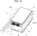
- FIG. 14 is a perspective view illustrating an external appearance of the power conversion device 200.
- the external appearance of the power change device 200 according to the present embodiment is formed by fixing a housing 12 having a substantially rectangular top or bottom surface, an upper casing 10 provided on one of a short-side outer periphery of the housing 12, and a lower case 16 for blocking a lower opening of the housing 12. Since the shape of the bottom view or the top view of the housing 12 is made substantially rectangular, installation to a vehicle is easy and production is easy.
- FIG. 15 is a schematic view illustrating a section structure of the power conversion device 200.
- the power semiconductor module 300 is installed in the channel forming body 1000 similarly to the installation structure illustrated in FIG. 4 .
- a laminated wiring board 501 on which components are mounted is assembled, and the signal terminals and the laminated wiring board 501 are electrically connected. Further, the terminals 320B, 315B, and 320B through which a large current flows are welded to terminals protruding from a plate 1200 on which bus bar wiring is laminated in multiple layers.
- the laminated wiring board 501 and the plate 1200 are stereoscopically laminated, thereby to downsize the power conversion device.
- the channel forming body 1000 forms a refrigerant channel into which a refrigerant for cooling the power semiconductor module 300 flows.
- the channel forming body 1000 has the wall surface 1001.
- the wall surface 1001 forms a channel through which the refrigerant flows between a heat dissipation portion 910 of the power semiconductor module 300 and the wall surface 1001.
- the wall surface 1001 has a planar structure not to allow the refrigerant to flow between the sealing resin surface 900B of the power semiconductor module 300 and the wall surface 1001.
- the channel forming body 1000 is formed such that the distance between the wall surfaces 1001 facing each other and the distance between the sealing resin surface 900B on one side and the sealing resin surface 900B on the other side, of the power semiconductor module 300, become substantially equal.
- An elastic body such as an O ring is provided on the sealing portion 901 of the power semiconductor module 300.
- the power semiconductor module 300 is inserted into the channel forming body 1000 such that the sealing resin surface 900B come in contact with the wall surface 1001 of the channel forming body 1000.
- the power semiconductor module 300 is disposed such that the tips of the fin portion 920 formed to be substantially flush with the sealing resin surface 900B come to contact with the wall surface 1001 of the channel forming body 1000. Therefore, the refrigerant flowing between the fin portion 920 and the wall surface 1001 is restrained from flowing between the sealing resin surface 900B and the wall surface 1001 and between the tips of the fins and the wall surface 1001 as a bypass flow.
- the heat dissipation portion 910 is configured from a high-temperature conductor 920 having high thermal conductivity, the heat of the power semiconductor device can be efficiently cooled. Therefore, the power semiconductor module 300 of the present embodiment is excellent in heat dissipation.
- the channel through which the refrigerant flows is configured from a combination of the fin structure formed on the power semiconductor module 300 side and the wall surface 1001 on a plane formed on the channel forming body 1000 side. With the simplification of the structure, the power conversion device can be easily manufactured.
- approximately the same plane means that planes are manufactured to become the same plane as much as possible. Steps that do not exceed 100 ⁇ m, such as a step caused by resin curing shrinkage or a difference in thermal expansion between members, and surface roughness, are less affected in suppressing the bypass flow and are therefore included in approximately the same plane.
- the channel forming body 1000 is not particularly limited as long as the channel forming body has a watertight structure.
- the channel forming body 1000 can be manufactured using metal such as aluminum or aluminum die cast, a thermoplastic resin such as polyphenylene sulfide, polybutylene terephthalate, polyamide, polyimide, or polytetrafluoroethylene, or a thermosetting resin such as an epoxy resin.
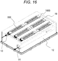
- FIG. 16 is a sectional view in a section A of FIG. 14 .
- the housing 12 forms the channel forming body 1000.
- the refrigerant flowing into the waterway 19 through a cooling water inlet 13 flows in the waterway 19 as indicated by the arrows and is discharged through a cooling water outlet 14.
- six power semiconductor devices 300 are arranged along the flow of cooling water in the waterway 19.
- an embodiment is not limited to the present embodiment, and metal plating is applied to a surface of the power semiconductor module 300 of the above-described embodiment, the surface being lower than the sealing portion and being in contact with the cooling water.
- the sealing resin is prevented from being directly in contact with the cooling water, and a decrease in chip insulating properties due to absorption of water by the sealing resin can be suppressed.
- FIG. 17 is a schematic view for describing a structure as a modification of a power semiconductor module of the present invention.
- a wall portion, a fin portion, and a stress support portion 1300 are illustrated by the solid lines, and a sealing resin and terminals are illustrated by broken lines.
- hatched members are the stress support portion 1300.
- the stress support portion 1300 is disposed directly under a wall portion 800 formed on an outer periphery of a fin portion 920.
- a plurality of the stress support portions 1300 is disposed.
- FIG. 18 is a schematic view of the power semiconductor module according to the modification illustrated in FIG. 17 at the time of transfer molding.
- the stress support portion 1300 is formed by connecting wiring patterns provided on a collector-side ceramic board and an emitter-side ceramic board with connecting material such as solder. Since the stress support portion is formed of the wiring patterns and the connecting member such as solder, an additional process or member for forming the stress support portion is unnecessary, and the productivity is excellent and the cost is low.
- the stress support portion 1300 supports mold clamping force at the time of transfer molding, thereby to reduce the stress applied to the semiconductor device to prevent device destruction.
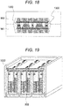
- FIG. 19 illustrates a sectional perspective view of a power conversion device according to a second embodiment.
- the point of difference from the first embodiment is that a terminal of a power semiconductor module comes out from one direction.
- the power semiconductor module of the present embodiment has an effect to facilitate insertion into a channel forming body 1000.
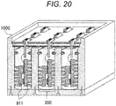
- FIG. 20 is a sectional perspective view of a power conversion device according to a third embodiment.
- a waterway forming body 1000 is made of a resin
- a power semiconductor module has no insulating layer
- a cooling medium is an insulating oil. Since the insulating oil is used as the cooling medium, an insulating layer is unnecessary inside the power semiconductor module, and the power conversion device can be downsized.
- FIG. 21 illustrates a schematic view of a power conversion device according to a comparative example. Since a fin portion 920 protrudes, a cooling medium flows not only into the vicinity of the fin portion 920 but also into upper and lower gaps, and a bypass flow 1002 is generated. With such a configuration, the flow rate of the fin portion having a narrow gap is greatly reduced as compared with the region where the bypass flow flows, and the heat dissipation is poor.
Landscapes
- Inverter Devices (AREA)
- Cooling Or The Like Of Semiconductors Or Solid State Devices (AREA)
- Chemical & Material Sciences (AREA)
- Dispersion Chemistry (AREA)
- Engineering & Computer Science (AREA)
- Microelectronics & Electronic Packaging (AREA)
Applications Claiming Priority (1)
| Application Number | Priority Date | Filing Date | Title |
|---|---|---|---|
| PCT/JP2015/073926 WO2017033295A1 (fr) | 2015-08-26 | 2015-08-26 | Structure |
Publications (3)
| Publication Number | Publication Date |
|---|---|
| EP3343603A1 true EP3343603A1 (fr) | 2018-07-04 |
| EP3343603A4 EP3343603A4 (fr) | 2019-04-24 |
| EP3343603B1 EP3343603B1 (fr) | 2020-05-20 |
Family
ID=58100718
Family Applications (1)
| Application Number | Title | Priority Date | Filing Date |
|---|---|---|---|
| EP15902264.9A Active EP3343603B1 (fr) | 2015-08-26 | 2015-08-26 | Structure |
Country Status (5)
| Country | Link |
|---|---|
| US (1) | US10818573B2 (fr) |
| EP (1) | EP3343603B1 (fr) |
| JP (1) | JP6488390B2 (fr) |
| CN (1) | CN107924885B (fr) |
| WO (1) | WO2017033295A1 (fr) |
Families Citing this family (10)
| Publication number | Priority date | Publication date | Assignee | Title |
|---|---|---|---|---|
| JP6922450B2 (ja) * | 2017-06-08 | 2021-08-18 | 株式会社デンソー | 半導体モジュール |
| JP2019057546A (ja) * | 2017-09-19 | 2019-04-11 | 東芝メモリ株式会社 | 半導体記憶装置 |
| JP7046742B2 (ja) * | 2018-07-05 | 2022-04-04 | 日立Astemo株式会社 | パワーモジュール |
| WO2021066044A1 (fr) * | 2019-10-04 | 2021-04-08 | 三井化学株式会社 | Boîtier et structure de logement d'élément chauffant |
| US12347741B2 (en) | 2020-01-08 | 2025-07-01 | Mitsubishi Electric Corporation | Semiconductor device comprising a resin member having a rib including a lower end located below lower ends of a plurality of pin fins and semiconductor device manufacturing method |
| DE102020111528A1 (de) * | 2020-04-28 | 2021-10-28 | Semikron Elektronik Gmbh & Co. Kg | Leistungselektronische Anordnung mit einem Mehrphasen-Leistungshalbleitermodul |
| JP7580233B2 (ja) * | 2020-10-01 | 2024-11-11 | 株式会社日立製作所 | 半導体装置およびホイール内蔵システム |
| FR3115651B1 (fr) * | 2020-10-26 | 2024-01-26 | Commissariat A L’Energie Atomique Et Aux Energies Alternatives | Ensemble de modules de puissance à semi-conducteurs |
| US11658171B2 (en) * | 2020-12-23 | 2023-05-23 | Semiconductor Components Industries, Llc | Dual cool power module with stress buffer layer |
| CN115249672B (zh) * | 2021-04-28 | 2025-01-14 | 比亚迪股份有限公司 | Igbt模组、电机控制器和车辆 |
Family Cites Families (18)
| Publication number | Priority date | Publication date | Assignee | Title |
|---|---|---|---|---|
| JPH10112519A (ja) | 1996-10-08 | 1998-04-28 | Nippon Motorola Ltd | 熱放散手段を有する集積回路装置及びその製造方法 |
| EP2234154B1 (fr) * | 2000-04-19 | 2016-03-30 | Denso Corporation | Dispositif semi-conducteur refroidi par un dissipateur de base à réfrigérant |
| JP4022758B2 (ja) | 2003-03-31 | 2007-12-19 | 株式会社デンソー | 半導体装置 |
| JP4379339B2 (ja) * | 2005-01-19 | 2009-12-09 | トヨタ自動車株式会社 | 半導体冷却装置 |
| JP4958735B2 (ja) * | 2007-11-01 | 2012-06-20 | 株式会社日立製作所 | パワー半導体モジュールの製造方法、パワー半導体モジュールの製造装置、パワー半導体モジュール、及び接合方法 |
| JP4580997B2 (ja) | 2008-03-11 | 2010-11-17 | 日立オートモティブシステムズ株式会社 | 電力変換装置 |
| JP5581131B2 (ja) * | 2010-06-30 | 2014-08-27 | 日立オートモティブシステムズ株式会社 | パワーモジュール及びそれを用いた電力変換装置 |
| JP5439309B2 (ja) * | 2010-07-28 | 2014-03-12 | 日立オートモティブシステムズ株式会社 | 電力変換装置 |
| JP2012164763A (ja) * | 2011-02-04 | 2012-08-30 | Toyota Motor Corp | ヒートシンク付き半導体パッケージの製造方法及び当該ヒートシンク |
| JP2013030649A (ja) | 2011-07-29 | 2013-02-07 | Mitsubishi Electric Corp | 半導体モジュール及びその製造方法 |
| JP5529208B2 (ja) | 2011-08-25 | 2014-06-25 | トヨタ自動車株式会社 | パワーモジュールの構造及び成形方法 |
| JPWO2013125474A1 (ja) | 2012-02-24 | 2015-07-30 | 三菱電機株式会社 | 半導体装置とその製造方法 |
| JP5879233B2 (ja) * | 2012-08-31 | 2016-03-08 | 日立オートモティブシステムズ株式会社 | パワー半導体モジュール |
| JP6187222B2 (ja) | 2013-12-13 | 2017-08-30 | トヨタ自動車株式会社 | 半導体モジュール |
| US9661738B1 (en) * | 2014-09-03 | 2017-05-23 | Flextronics Ap, Llc | Embedded coins for HDI or SEQ laminations |
| CN105514080B (zh) * | 2014-10-11 | 2018-12-04 | 意法半导体有限公司 | 具有再分布层和加强件的电子器件及相关方法 |
| JP6349275B2 (ja) | 2015-03-05 | 2018-06-27 | 日立オートモティブシステムズ株式会社 | 電力変換装置 |
| US9659844B2 (en) * | 2015-08-31 | 2017-05-23 | Texas Instruments Incorporated | Semiconductor die substrate with integral heat sink |
-
2015
- 2015-08-26 JP JP2017536120A patent/JP6488390B2/ja active Active
- 2015-08-26 WO PCT/JP2015/073926 patent/WO2017033295A1/fr not_active Ceased
- 2015-08-26 CN CN201580082498.3A patent/CN107924885B/zh active Active
- 2015-08-26 EP EP15902264.9A patent/EP3343603B1/fr active Active
- 2015-08-26 US US15/753,763 patent/US10818573B2/en active Active
Also Published As
| Publication number | Publication date |
|---|---|
| CN107924885A (zh) | 2018-04-17 |
| JP6488390B2 (ja) | 2019-03-20 |
| JPWO2017033295A1 (ja) | 2018-07-05 |
| EP3343603A4 (fr) | 2019-04-24 |
| EP3343603B1 (fr) | 2020-05-20 |
| US20180254235A1 (en) | 2018-09-06 |
| CN107924885B (zh) | 2020-08-25 |
| US10818573B2 (en) | 2020-10-27 |
| WO2017033295A1 (fr) | 2017-03-02 |
Similar Documents
| Publication | Publication Date | Title |
|---|---|---|
| EP3343603B1 (fr) | Structure | |
| CN111373524B (zh) | 功率半导体装置及其制造方法 | |
| CN113016068B (zh) | 半导体模块、功率转换装置及半导体模块的制作方法 | |
| JP6237912B2 (ja) | パワー半導体モジュール | |
| JP6302803B2 (ja) | パワー半導体モジュール及びその製造方法、電力変換装置 | |
| US9806009B2 (en) | Semiconductor device and power converter using the same | |
| CN112335043B (zh) | 功率模块 | |
| JP7555257B2 (ja) | 電気回路体、電力変換装置、および電気回路体の製造方法 | |
| CN115088065A (zh) | 电路体、电力转换装置及电路体的制造方法 | |
| JP2015095560A (ja) | パワーモジュール | |
| US9437508B2 (en) | Method for manufacturing semiconductor device and semiconductor device | |
| WO2018159209A1 (fr) | Dispositif à semiconducteur de puissance | |
| US20200227333A1 (en) | Power Semiconductor Device and Power Conversion Apparatus Including the Same | |
| CN220856564U (zh) | 功率模块 | |
| JP7555261B2 (ja) | 電気回路体および電力変換装置 | |
| JP7555262B2 (ja) | 電気回路体および電力変換装置 | |
| CN119452471A (zh) | 电路体和功率转换装置 | |
| CN214756105U (zh) | 逆变器模块及逆变器 | |
| JP7650784B2 (ja) | 半導体モジュール、電力変換装置、および半導体モジュールの製造方法 |
Legal Events
| Date | Code | Title | Description |
|---|---|---|---|
| STAA | Information on the status of an ep patent application or granted ep patent |
Free format text: STATUS: THE INTERNATIONAL PUBLICATION HAS BEEN MADE |
|
| PUAI | Public reference made under article 153(3) epc to a published international application that has entered the european phase |
Free format text: ORIGINAL CODE: 0009012 |
|
| STAA | Information on the status of an ep patent application or granted ep patent |
Free format text: STATUS: REQUEST FOR EXAMINATION WAS MADE |
|
| 17P | Request for examination filed |
Effective date: 20180326 |
|
| AK | Designated contracting states |
Kind code of ref document: A1 Designated state(s): AL AT BE BG CH CY CZ DE DK EE ES FI FR GB GR HR HU IE IS IT LI LT LU LV MC MK MT NL NO PL PT RO RS SE SI SK SM TR |
|
| AX | Request for extension of the european patent |
Extension state: BA ME |
|
| DAV | Request for validation of the european patent (deleted) | ||
| DAX | Request for extension of the european patent (deleted) | ||
| REG | Reference to a national code |
Ref country code: DE Ref legal event code: R079 Ref document number: 602015053200 Country of ref document: DE Free format text: PREVIOUS MAIN CLASS: H01L0023290000 Ipc: H01L0023473000 |
|
| A4 | Supplementary search report drawn up and despatched |
Effective date: 20190327 |
|
| RIC1 | Information provided on ipc code assigned before grant |
Ipc: H01L 25/07 20060101ALI20190321BHEP Ipc: H01L 23/473 20060101AFI20190321BHEP |
|
| GRAP | Despatch of communication of intention to grant a patent |
Free format text: ORIGINAL CODE: EPIDOSNIGR1 |
|
| STAA | Information on the status of an ep patent application or granted ep patent |
Free format text: STATUS: GRANT OF PATENT IS INTENDED |
|
| INTG | Intention to grant announced |
Effective date: 20200113 |
|
| GRAS | Grant fee paid |
Free format text: ORIGINAL CODE: EPIDOSNIGR3 |
|
| GRAA | (expected) grant |
Free format text: ORIGINAL CODE: 0009210 |
|
| STAA | Information on the status of an ep patent application or granted ep patent |
Free format text: STATUS: THE PATENT HAS BEEN GRANTED |
|
| AK | Designated contracting states |
Kind code of ref document: B1 Designated state(s): AL AT BE BG CH CY CZ DE DK EE ES FI FR GB GR HR HU IE IS IT LI LT LU LV MC MK MT NL NO PL PT RO RS SE SI SK SM TR |
|
| REG | Reference to a national code |
Ref country code: GB Ref legal event code: FG4D |
|
| REG | Reference to a national code |
Ref country code: CH Ref legal event code: EP |
|
| REG | Reference to a national code |
Ref country code: DE Ref legal event code: R096 Ref document number: 602015053200 Country of ref document: DE |
|
| REG | Reference to a national code |
Ref country code: AT Ref legal event code: REF Ref document number: 1273178 Country of ref document: AT Kind code of ref document: T Effective date: 20200615 |
|
| REG | Reference to a national code |
Ref country code: LT Ref legal event code: MG4D |
|
| REG | Reference to a national code |
Ref country code: NL Ref legal event code: MP Effective date: 20200520 |
|
| PG25 | Lapsed in a contracting state [announced via postgrant information from national office to epo] |
Ref country code: PT Free format text: LAPSE BECAUSE OF FAILURE TO SUBMIT A TRANSLATION OF THE DESCRIPTION OR TO PAY THE FEE WITHIN THE PRESCRIBED TIME-LIMIT Effective date: 20200921 Ref country code: NO Free format text: LAPSE BECAUSE OF FAILURE TO SUBMIT A TRANSLATION OF THE DESCRIPTION OR TO PAY THE FEE WITHIN THE PRESCRIBED TIME-LIMIT Effective date: 20200820 Ref country code: GR Free format text: LAPSE BECAUSE OF FAILURE TO SUBMIT A TRANSLATION OF THE DESCRIPTION OR TO PAY THE FEE WITHIN THE PRESCRIBED TIME-LIMIT Effective date: 20200821 Ref country code: FI Free format text: LAPSE BECAUSE OF FAILURE TO SUBMIT A TRANSLATION OF THE DESCRIPTION OR TO PAY THE FEE WITHIN THE PRESCRIBED TIME-LIMIT Effective date: 20200520 Ref country code: IS Free format text: LAPSE BECAUSE OF FAILURE TO SUBMIT A TRANSLATION OF THE DESCRIPTION OR TO PAY THE FEE WITHIN THE PRESCRIBED TIME-LIMIT Effective date: 20200920 Ref country code: SE Free format text: LAPSE BECAUSE OF FAILURE TO SUBMIT A TRANSLATION OF THE DESCRIPTION OR TO PAY THE FEE WITHIN THE PRESCRIBED TIME-LIMIT Effective date: 20200520 Ref country code: LT Free format text: LAPSE BECAUSE OF FAILURE TO SUBMIT A TRANSLATION OF THE DESCRIPTION OR TO PAY THE FEE WITHIN THE PRESCRIBED TIME-LIMIT Effective date: 20200520 |
|
| PG25 | Lapsed in a contracting state [announced via postgrant information from national office to epo] |
Ref country code: BG Free format text: LAPSE BECAUSE OF FAILURE TO SUBMIT A TRANSLATION OF THE DESCRIPTION OR TO PAY THE FEE WITHIN THE PRESCRIBED TIME-LIMIT Effective date: 20200820 Ref country code: LV Free format text: LAPSE BECAUSE OF FAILURE TO SUBMIT A TRANSLATION OF THE DESCRIPTION OR TO PAY THE FEE WITHIN THE PRESCRIBED TIME-LIMIT Effective date: 20200520 Ref country code: HR Free format text: LAPSE BECAUSE OF FAILURE TO SUBMIT A TRANSLATION OF THE DESCRIPTION OR TO PAY THE FEE WITHIN THE PRESCRIBED TIME-LIMIT Effective date: 20200520 Ref country code: RS Free format text: LAPSE BECAUSE OF FAILURE TO SUBMIT A TRANSLATION OF THE DESCRIPTION OR TO PAY THE FEE WITHIN THE PRESCRIBED TIME-LIMIT Effective date: 20200520 |
|
| REG | Reference to a national code |
Ref country code: AT Ref legal event code: MK05 Ref document number: 1273178 Country of ref document: AT Kind code of ref document: T Effective date: 20200520 |
|
| PG25 | Lapsed in a contracting state [announced via postgrant information from national office to epo] |
Ref country code: NL Free format text: LAPSE BECAUSE OF FAILURE TO SUBMIT A TRANSLATION OF THE DESCRIPTION OR TO PAY THE FEE WITHIN THE PRESCRIBED TIME-LIMIT Effective date: 20200520 Ref country code: AL Free format text: LAPSE BECAUSE OF FAILURE TO SUBMIT A TRANSLATION OF THE DESCRIPTION OR TO PAY THE FEE WITHIN THE PRESCRIBED TIME-LIMIT Effective date: 20200520 |
|
| PG25 | Lapsed in a contracting state [announced via postgrant information from national office to epo] |
Ref country code: DK Free format text: LAPSE BECAUSE OF FAILURE TO SUBMIT A TRANSLATION OF THE DESCRIPTION OR TO PAY THE FEE WITHIN THE PRESCRIBED TIME-LIMIT Effective date: 20200520 Ref country code: AT Free format text: LAPSE BECAUSE OF FAILURE TO SUBMIT A TRANSLATION OF THE DESCRIPTION OR TO PAY THE FEE WITHIN THE PRESCRIBED TIME-LIMIT Effective date: 20200520 Ref country code: EE Free format text: LAPSE BECAUSE OF FAILURE TO SUBMIT A TRANSLATION OF THE DESCRIPTION OR TO PAY THE FEE WITHIN THE PRESCRIBED TIME-LIMIT Effective date: 20200520 Ref country code: SM Free format text: LAPSE BECAUSE OF FAILURE TO SUBMIT A TRANSLATION OF THE DESCRIPTION OR TO PAY THE FEE WITHIN THE PRESCRIBED TIME-LIMIT Effective date: 20200520 Ref country code: IT Free format text: LAPSE BECAUSE OF FAILURE TO SUBMIT A TRANSLATION OF THE DESCRIPTION OR TO PAY THE FEE WITHIN THE PRESCRIBED TIME-LIMIT Effective date: 20200520 Ref country code: ES Free format text: LAPSE BECAUSE OF FAILURE TO SUBMIT A TRANSLATION OF THE DESCRIPTION OR TO PAY THE FEE WITHIN THE PRESCRIBED TIME-LIMIT Effective date: 20200520 Ref country code: RO Free format text: LAPSE BECAUSE OF FAILURE TO SUBMIT A TRANSLATION OF THE DESCRIPTION OR TO PAY THE FEE WITHIN THE PRESCRIBED TIME-LIMIT Effective date: 20200520 Ref country code: CZ Free format text: LAPSE BECAUSE OF FAILURE TO SUBMIT A TRANSLATION OF THE DESCRIPTION OR TO PAY THE FEE WITHIN THE PRESCRIBED TIME-LIMIT Effective date: 20200520 |
|
| REG | Reference to a national code |
Ref country code: DE Ref legal event code: R097 Ref document number: 602015053200 Country of ref document: DE |
|
| PG25 | Lapsed in a contracting state [announced via postgrant information from national office to epo] |
Ref country code: PL Free format text: LAPSE BECAUSE OF FAILURE TO SUBMIT A TRANSLATION OF THE DESCRIPTION OR TO PAY THE FEE WITHIN THE PRESCRIBED TIME-LIMIT Effective date: 20200520 Ref country code: SK Free format text: LAPSE BECAUSE OF FAILURE TO SUBMIT A TRANSLATION OF THE DESCRIPTION OR TO PAY THE FEE WITHIN THE PRESCRIBED TIME-LIMIT Effective date: 20200520 |
|
| REG | Reference to a national code |
Ref country code: DE Ref legal event code: R082 Ref document number: 602015053200 Country of ref document: DE Representative=s name: MANITZ FINSTERWALD PATENT- UND RECHTSANWALTSPA, DE Ref country code: DE Ref legal event code: R081 Ref document number: 602015053200 Country of ref document: DE Owner name: HITACHI ASTEMO, LTD., HITACHINAKA-SHI, JP Free format text: FORMER OWNER: HITACHI AUTOMOTIVE SYSTEMS, LTD., HITACHINAKA-SHI, IBARAKI, JP |
|
| PLBE | No opposition filed within time limit |
Free format text: ORIGINAL CODE: 0009261 |
|
| STAA | Information on the status of an ep patent application or granted ep patent |
Free format text: STATUS: NO OPPOSITION FILED WITHIN TIME LIMIT |
|
| PG25 | Lapsed in a contracting state [announced via postgrant information from national office to epo] |
Ref country code: MC Free format text: LAPSE BECAUSE OF FAILURE TO SUBMIT A TRANSLATION OF THE DESCRIPTION OR TO PAY THE FEE WITHIN THE PRESCRIBED TIME-LIMIT Effective date: 20200520 |
|
| REG | Reference to a national code |
Ref country code: CH Ref legal event code: PL |
|
| 26N | No opposition filed |
Effective date: 20210223 |
|
| GBPC | Gb: european patent ceased through non-payment of renewal fee |
Effective date: 20200826 |
|
| PG25 | Lapsed in a contracting state [announced via postgrant information from national office to epo] |
Ref country code: CH Free format text: LAPSE BECAUSE OF NON-PAYMENT OF DUE FEES Effective date: 20200831 Ref country code: LU Free format text: LAPSE BECAUSE OF NON-PAYMENT OF DUE FEES Effective date: 20200826 Ref country code: LI Free format text: LAPSE BECAUSE OF NON-PAYMENT OF DUE FEES Effective date: 20200831 |
|
| REG | Reference to a national code |
Ref country code: BE Ref legal event code: MM Effective date: 20200831 |
|
| PG25 | Lapsed in a contracting state [announced via postgrant information from national office to epo] |
Ref country code: SI Free format text: LAPSE BECAUSE OF FAILURE TO SUBMIT A TRANSLATION OF THE DESCRIPTION OR TO PAY THE FEE WITHIN THE PRESCRIBED TIME-LIMIT Effective date: 20200520 |
|
| PG25 | Lapsed in a contracting state [announced via postgrant information from national office to epo] |
Ref country code: FR Free format text: LAPSE BECAUSE OF NON-PAYMENT OF DUE FEES Effective date: 20200831 |
|
| PG25 | Lapsed in a contracting state [announced via postgrant information from national office to epo] |
Ref country code: GB Free format text: LAPSE BECAUSE OF NON-PAYMENT OF DUE FEES Effective date: 20200826 Ref country code: IE Free format text: LAPSE BECAUSE OF NON-PAYMENT OF DUE FEES Effective date: 20200826 Ref country code: BE Free format text: LAPSE BECAUSE OF NON-PAYMENT OF DUE FEES Effective date: 20200831 |
|
| PG25 | Lapsed in a contracting state [announced via postgrant information from national office to epo] |
Ref country code: TR Free format text: LAPSE BECAUSE OF FAILURE TO SUBMIT A TRANSLATION OF THE DESCRIPTION OR TO PAY THE FEE WITHIN THE PRESCRIBED TIME-LIMIT Effective date: 20200520 Ref country code: MT Free format text: LAPSE BECAUSE OF FAILURE TO SUBMIT A TRANSLATION OF THE DESCRIPTION OR TO PAY THE FEE WITHIN THE PRESCRIBED TIME-LIMIT Effective date: 20200520 Ref country code: CY Free format text: LAPSE BECAUSE OF FAILURE TO SUBMIT A TRANSLATION OF THE DESCRIPTION OR TO PAY THE FEE WITHIN THE PRESCRIBED TIME-LIMIT Effective date: 20200520 |
|
| PG25 | Lapsed in a contracting state [announced via postgrant information from national office to epo] |
Ref country code: MK Free format text: LAPSE BECAUSE OF FAILURE TO SUBMIT A TRANSLATION OF THE DESCRIPTION OR TO PAY THE FEE WITHIN THE PRESCRIBED TIME-LIMIT Effective date: 20200520 |
|
| PGFP | Annual fee paid to national office [announced via postgrant information from national office to epo] |
Ref country code: DE Payment date: 20250702 Year of fee payment: 11 |
|
| REG | Reference to a national code |
Ref country code: DE Ref legal event code: R079 Ref document number: 602015053200 Country of ref document: DE Free format text: PREVIOUS MAIN CLASS: H01L0023473000 Ipc: H10W0040470000 |