EP3343636A1 - Structure semi-conductrice igbt - Google Patents
Structure semi-conductrice igbt Download PDFInfo
- Publication number
- EP3343636A1 EP3343636A1 EP17002087.9A EP17002087A EP3343636A1 EP 3343636 A1 EP3343636 A1 EP 3343636A1 EP 17002087 A EP17002087 A EP 17002087A EP 3343636 A1 EP3343636 A1 EP 3343636A1
- Authority
- EP
- European Patent Office
- Prior art keywords
- semiconductor structure
- layer
- igbt semiconductor
- region
- dopant concentration
- Prior art date
- Legal status (The legal status is an assumption and is not a legal conclusion. Google has not performed a legal analysis and makes no representation as to the accuracy of the status listed.)
- Granted
Links
Images

Classifications
-
- H—ELECTRICITY
- H10—SEMICONDUCTOR DEVICES; ELECTRIC SOLID-STATE DEVICES NOT OTHERWISE PROVIDED FOR
- H10D—INORGANIC ELECTRIC SEMICONDUCTOR DEVICES
- H10D12/00—Bipolar devices controlled by the field effect, e.g. insulated-gate bipolar transistors [IGBT]
- H10D12/411—Insulated-gate bipolar transistors [IGBT]
- H10D12/441—Vertical IGBTs
- H10D12/491—Vertical IGBTs having both emitter contacts and collector contacts in the same substrate side
-
- H—ELECTRICITY
- H10—SEMICONDUCTOR DEVICES; ELECTRIC SOLID-STATE DEVICES NOT OTHERWISE PROVIDED FOR
- H10D—INORGANIC ELECTRIC SEMICONDUCTOR DEVICES
- H10D12/00—Bipolar devices controlled by the field effect, e.g. insulated-gate bipolar transistors [IGBT]
- H10D12/411—Insulated-gate bipolar transistors [IGBT]
- H10D12/441—Vertical IGBTs
-
- H—ELECTRICITY
- H10—SEMICONDUCTOR DEVICES; ELECTRIC SOLID-STATE DEVICES NOT OTHERWISE PROVIDED FOR
- H10D—INORGANIC ELECTRIC SEMICONDUCTOR DEVICES
- H10D12/00—Bipolar devices controlled by the field effect, e.g. insulated-gate bipolar transistors [IGBT]
- H10D12/411—Insulated-gate bipolar transistors [IGBT]
- H10D12/441—Vertical IGBTs
- H10D12/461—Vertical IGBTs having non-planar surfaces, e.g. having trenches, recesses or pillars in the surfaces of the emitter, base or collector regions
- H10D12/481—Vertical IGBTs having non-planar surfaces, e.g. having trenches, recesses or pillars in the surfaces of the emitter, base or collector regions having gate structures on slanted surfaces, on vertical surfaces, or in grooves, e.g. trench gate IGBTs
-
- H—ELECTRICITY
- H10—SEMICONDUCTOR DEVICES; ELECTRIC SOLID-STATE DEVICES NOT OTHERWISE PROVIDED FOR
- H10D—INORGANIC ELECTRIC SEMICONDUCTOR DEVICES
- H10D62/00—Semiconductor bodies, or regions thereof, of devices having potential barriers
- H10D62/10—Shapes, relative sizes or dispositions of the regions of the semiconductor bodies; Shapes of the semiconductor bodies
- H10D62/124—Shapes, relative sizes or dispositions of the regions of semiconductor bodies or of junctions between the regions
-
- H—ELECTRICITY
- H10—SEMICONDUCTOR DEVICES; ELECTRIC SOLID-STATE DEVICES NOT OTHERWISE PROVIDED FOR
- H10D—INORGANIC ELECTRIC SEMICONDUCTOR DEVICES
- H10D62/00—Semiconductor bodies, or regions thereof, of devices having potential barriers
- H10D62/10—Shapes, relative sizes or dispositions of the regions of the semiconductor bodies; Shapes of the semiconductor bodies
- H10D62/124—Shapes, relative sizes or dispositions of the regions of semiconductor bodies or of junctions between the regions
- H10D62/126—Top-view geometrical layouts of the regions or the junctions
- H10D62/127—Top-view geometrical layouts of the regions or the junctions of cellular field-effect devices, e.g. multicellular DMOS transistors or IGBTs
-
- H—ELECTRICITY
- H10—SEMICONDUCTOR DEVICES; ELECTRIC SOLID-STATE DEVICES NOT OTHERWISE PROVIDED FOR
- H10D—INORGANIC ELECTRIC SEMICONDUCTOR DEVICES
- H10D62/00—Semiconductor bodies, or regions thereof, of devices having potential barriers
- H10D62/10—Shapes, relative sizes or dispositions of the regions of the semiconductor bodies; Shapes of the semiconductor bodies
- H10D62/17—Semiconductor regions connected to electrodes not carrying current to be rectified, amplified or switched, e.g. channel regions
- H10D62/213—Channel regions of field-effect devices
- H10D62/221—Channel regions of field-effect devices of FETs
- H10D62/235—Channel regions of field-effect devices of FETs of IGFETs
- H10D62/314—Channel regions of field-effect devices of FETs of IGFETs having vertical doping variations
-
- H—ELECTRICITY
- H10—SEMICONDUCTOR DEVICES; ELECTRIC SOLID-STATE DEVICES NOT OTHERWISE PROVIDED FOR
- H10D—INORGANIC ELECTRIC SEMICONDUCTOR DEVICES
- H10D62/00—Semiconductor bodies, or regions thereof, of devices having potential barriers
- H10D62/60—Impurity distributions or concentrations
-
- H—ELECTRICITY
- H10—SEMICONDUCTOR DEVICES; ELECTRIC SOLID-STATE DEVICES NOT OTHERWISE PROVIDED FOR
- H10D—INORGANIC ELECTRIC SEMICONDUCTOR DEVICES
- H10D62/00—Semiconductor bodies, or regions thereof, of devices having potential barriers
- H10D62/80—Semiconductor bodies, or regions thereof, of devices having potential barriers characterised by the materials
- H10D62/85—Semiconductor bodies, or regions thereof, of devices having potential barriers characterised by the materials being Group III-V materials, e.g. GaAs
-
- H—ELECTRICITY
- H10—SEMICONDUCTOR DEVICES; ELECTRIC SOLID-STATE DEVICES NOT OTHERWISE PROVIDED FOR
- H10D—INORGANIC ELECTRIC SEMICONDUCTOR DEVICES
- H10D62/00—Semiconductor bodies, or regions thereof, of devices having potential barriers
- H10D62/80—Semiconductor bodies, or regions thereof, of devices having potential barriers characterised by the materials
- H10D62/85—Semiconductor bodies, or regions thereof, of devices having potential barriers characterised by the materials being Group III-V materials, e.g. GaAs
- H10D62/854—Semiconductor bodies, or regions thereof, of devices having potential barriers characterised by the materials being Group III-V materials, e.g. GaAs further characterised by the dopants
-
- H—ELECTRICITY
- H10—SEMICONDUCTOR DEVICES; ELECTRIC SOLID-STATE DEVICES NOT OTHERWISE PROVIDED FOR
- H10D—INORGANIC ELECTRIC SEMICONDUCTOR DEVICES
- H10D64/00—Electrodes of devices having potential barriers
- H10D64/111—Field plates
-
- H—ELECTRICITY
- H10—SEMICONDUCTOR DEVICES; ELECTRIC SOLID-STATE DEVICES NOT OTHERWISE PROVIDED FOR
- H10D—INORGANIC ELECTRIC SEMICONDUCTOR DEVICES
- H10D12/00—Bipolar devices controlled by the field effect, e.g. insulated-gate bipolar transistors [IGBT]
- H10D12/411—Insulated-gate bipolar transistors [IGBT]
- H10D12/441—Vertical IGBTs
- H10D12/461—Vertical IGBTs having non-planar surfaces, e.g. having trenches, recesses or pillars in the surfaces of the emitter, base or collector regions
Definitions
- the invention relates to an IGBT semiconductor structure having a p + substrate, an n - layer, a p region, an n + region, a dielectric layer and three connection contacts.
- IGBTs are known in various embodiments. Such power devices are manufactured on the basis of silicon or SIC.
- a high-voltage-resistant semiconductor diode p + -n-n + and a high-voltage pnip transistor based on GaAs is made of " GaAs Power Devices "by German Ashkinazi, ISBN 965-7094-19-4, Chapter 5, p. 97 or Chapter 7.8, p. 225 known.
- a deposition of oxide layers on GaAs for example by means of an atomic layer deposition (ALD) process is described in the articles " New Insight into Fermi-Level Unpinning on GaAs: Impact of Different Surface Orientations ", M. Xu et al., Electron Device Meeting (IEDM), IEEE, 2009, pp. 865-868 , and in " Impact of Buffer Layer on Atomic Layer Deposited TiAlO Alloy Dielectric Quality for Epitaxial GaAs / Ge Device Application ", GK Dalapati et al., IEEE Transactions on Electron Devices, Vol. 60, No. 1, 2013 described.
- ALD atomic layer deposition
- the object of the invention is to provide a device which further develops the prior art.
- an IGBT semiconductor structure having a top and a bottom is provided.
- the IGBT has a semiconductor structure formed on the underside of the IGBT semiconductor structure p + substrate and lying on the p + substrate n - -layer on.
- the n - layer has an adjacent p region and at least one n + region adjacent to the p region.
- the p + substrate has a dopant concentration of 5 * 10 18 -5 * 10 20 cm -3 and a layer thickness of 50-500 microns.
- the n - layer has a dopant concentration of 10 12 -10 17 cm -3 and a layer thickness of 10-300 microns.
- the at least one p-type region has a dopant concentration of 10 14 -10 18 cm -3 and the at least one n + -region has a dopant concentration of at least 10 19 cm -3 , the at least one p-type region having the n - layer forms a first pn junction.
- the one n + region forms a second pn junction with the one p region.
- the p * substrate, the n - layer, the p region and the n + region each comprise a GaAs compound or each consist of a GaAs compound.
- the first terminal contact, the second terminal contact and the third terminal contact each comprise a metal or a metal compound or each consist of a metal or a metal compound, wherein the second terminal contact is formed as a field plate on the dielectric layer.
- the third connection contact is electrically conductively connected to the at least one p-region and the at least one n + -region.
- connection contacts are preferably each arranged on the surface of the semiconductor structure.
- the dielectric layer covers at least the first pn junction and the second pn junction and is connected in a materially connected manner to the n - layer, the p region and the n + region.
- a doped intermediate layer having a layer thickness of 1 ⁇ m-50 ⁇ m and a dopant concentration of 10 12 -10 17 cm -3 is arranged between the p + substrate and the n - layer, wherein the intermediate layer at least with the p + substrate is connected cohesively.
- the second terminal contact is referred to as a gate.
- the first terminal is typically referred to as a collector or anode, while the third terminal is referred to as an emitter or cathode.
- connection contacts are each electrically conductive and have metallic properties and preferably comprise or consist of metallically conductive semiconductor layers or metal layers or a combination of the two.
- the connection contacts establish an electrically low-resistance contact with the directly adjacent doped semiconductor layers.
- connection contacts are preferably connected by means of bonding wires with contact fingers, the so-called pins.
- the intermediate layer has at least one different dopant concentration compared to the adjacent layers.
- GaAs semiconductor structures have a smaller effective mass compared to silicon carriers. Also, in comparison to Si, higher temperatures can be achieved at the pn junctions without the components being destroyed. As a result, higher switching frequencies and lower losses can be achieved with the GAs semiconductor structures than with the comparable SI semiconductor structures.
- III-IV IGBT semiconductor structure can be produced more cost-effectively than comparable semiconductor structures made of SiC.
- III-V-IGBT semiconductor structure is a high temperature resistance of up to 300 ° C.
- the III-V semiconductor diodes can also be used in hot environments.
- the intermediate layer is p-doped and, according to alternative developments, comprises zinc and / or silicon as dopants.
- the dopant concentration of the intermediate layer is preferably smaller than the dopant concentration of the p + substrate. More preferably, the dopant concentration is smaller in a range between a factor of 2 to a factor of five orders of magnitude.
- the intermediate layer is n-doped and preferably comprises silicon and / or tin as a dopant.
- the dopant concentration of the intermediate layer is preferably smaller than the dopant concentration of the n + substrate. Particularly preferably, the dopant concentration is up to a factor of 100 smaller than the dopant concentration of the n - layer.
- the IGBT semiconductor structure has an n-doped buffer layer, wherein the buffer layer between the intermediate layer and the n - layer is disposed, has a dopant concentration of 10 12 -10 16 cm -3 and a layer thickness of 1 ⁇ m-50 ⁇ m and comprises a GaAs compound or consists of a GaAs compound.
- the IGBT semiconductor structure is formed as a trench IGBT semiconductor structure, wherein the dielectric layer is perpendicular to the top of the IGBT semiconductor structure.
- the p + substrate preferably comprises zinc.
- the n - layer and / or the n + region preferably comprise silicon and / or chromium and / or palladium and / or tin, wherein the IGBZ semiconductor structure is particularly preferably monolithic.
- an overall height of the IGBT semiconductor structure is at most 150-500 ⁇ m and / or an edge length or a diameter of the IGBT semiconductor structure is between 1 mm and 15 mm.
- the p-region and / or the n-region are formed on the upper side of the IGBT semiconductor structure circular or straight with each arranged on the front side of the structures semicircles.
- the dielectric layer comprises a deposited oxide and has a layer thickness of 10 nm to 1 ⁇ m.
- the stacked layer structure has a semiconductor bond formed between the n - layer and the p + substrate.
- semiconductor bond is used synonymously with the term wafer-bond.
- the layer structure consisting of a p + substrate forms a first partial stack and the layer structure consisting of the n + -layer one of the n - layer and optionally the buffer layer a second sub-stack.
- the first part stack comprises the intermediate layer.
- the semiconductor bond is disposed between the intermediate layer and the n - layer or between the intermediate layer and the buffer layer.
- the first partial stack and the second partial stack are each formed monolithically.
- the first partial stack is formed, in which, starting from a p + -substrate, the intermediate layer is produced by means of epitaxy.
- the intermediate layer formed as p - layer has a doping less than 10 13 N / cm -3 , ie, the intermediate layer is intrinsically doped, or a doping between 10 13 N / cm -3 and 10 15 N / cm -3 .
- the p + substrate is thinned before or after bonding by a grinding process to a thickness of between 200 ⁇ m and 500 ⁇ m.
- the second stack is formed, in which, starting from an n - substrate, the n - substrate is connected to the second stack, ie, to the n + layer by a wafer bonding process.
- the n + layer is formed as an n + substrate.
- the n - substrate is thinned to the desired thickness.
- Substrate and the n - - -layer generates the buffer layer by means of an epitaxy, in a development, after the thin n.
- the thickness of the n - substrate or the n - layer is in a range between 50 microns to 250 microns.
- the doping of the n - substrate is located in a range between 10 13 N / cm -3 and 10 15 N / cm -3 .
- the n - substrate has a doping greater than 10 10 N / cm -3 and less than 10 13 N / cm -3 . In that the doping is extremely low, the n - substrate can also be considered as an intrinsic layer.
- the thinning of the n - substrate preferably takes place by means of a CMP step, ie by means of chemical mechanical polishing.
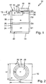
- the picture of the FIG. 1 shows a sectional view of a first embodiment of an IGBT semiconductor structure 10 with three terminal contacts 14, 16, 18 and a dielectric layer 20.
- the IGBT semiconductor structure 10, hereinafter also referred to as a semiconductor structure 10 is stacked with a top 12 and a bottom 22 is formed and has in the illustrated embodiment, a so-called non-punch-through design and a total height H1.
- the first connection contact 14 is formed as a metal layer, wherein the metal layer is materially connected to the underside 22 of the semiconductor structure 10.
- the lowermost layer of the IGBT semiconductor structure forms a p + substrate 24.
- the p + substrate thus forms the underside 22 of the semiconductor structure 10 and has a layer thickness D1.
- the p + substrate is followed by a thin, weakly n- or weakly p-doped intermediate layer 26 with a layer thickness D3 and an n - layer 28 with a layer thickness D2 in the order mentioned.
- the n - layer 28 forms at least part of the upper side 12 of the semiconductor structure 10.
- Another part of Top surface 12 of the semiconductor structure 10 is formed by a p-type region 32, wherein the p-region 32 from the top 12 of the IGBT semiconductor structure 10 to a depth T1 in the n - layer extends.
- a further part of the upper side 12 of the semiconductor structure 10 is formed by an n + region 34, the n + region extending from the upper side 12 of the semiconductor structure 10 to a depth T2 into the p-region and T2 being smaller than T1 ,
- a first pn junction 36 between the p region and the n form at the top surface 12 of the semiconductor structure 10 adjacent - layer and a second p-n junction 38 between the n + region and the p-type region of, the Dielectric layer 20 at least the first pn junction 36 and the second pn junction 38 is covered and connected to the top 12 of the semiconductor structure 10, in particular with the n + region, the p-region and the n - layer cohesively and a Layer thickness D5 has.
- the second connection contact 16 is formed as a field plate on a surface of the dielectric layer 20 facing away from the semiconductor structure 10.
- the third terminal contact 18 is also formed as a metal layer, wherein the metal layer is integrally connected to a part of the top surface 12 of the semiconductor structure 10 formed by the p-region and by the n + region.
- n + region 34, p region 32 and the n - layer 28 thus form together with the dielectric layer 16 and the three terminal contacts 14, 16, 18, a MOS transistor, a bipolar component, while p-type substrate 24 , Interlayer 26 and n - layer 28 represent a pin diode.
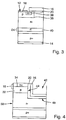
- FIG. 2 shows a top view of the top side 12 of the IGBT semiconductor structure 10. Both the p-region 32 and the n + -region 34 are circular.
- the IGBT semiconductor structure 10 has a rectangular upper side 12 with a first Katenat K1 and a second edge length K2.
- the semiconductor structure 10 is formed as a so-called punch-through IGBT, wherein between the intermediate layer 26 and the n-layer 28, a weakly n- or p-doped buffer layer 40 is arranged with a layer thickness D4.
- FIG. 4 a further embodiment of an IGBT semiconductor structure 10 is shown. The following are just the differences to the illustrations of FIGS. 1 and 3 explained.
- the semiconductor structure 10 is formed as a so-called trench IGBT.
- the p-type region 32 and the n + -region 34 are each formed as layers on the n -type layer or the p-type region 32, wherein the semiconductor structure 10 has a top surface 12 through the layered n-type region and the layered p-type region. Area up into the n - layer into reaching trench 42, the so-called trench has.
- the first pn junction 36 and the second pn junction 38 are perpendicular to a side surface 44 of the trench 42.
- the side surface 44 and a bottom 46 of the trench are covered with the dielectric layer 20.
- the second terminal contact 16 formed as a field plate extends correspondingly on the dielectric layer 20.
- the third terminal contact 18 is arranged on a side surface 44 of the trench 42 opposite side surface 50 of the semiconductor structure 10 and with the layered n + region 34 and with the layered p-. Area 32 electrically conductively connected.
- the third terminal contact 18 is arranged on the upper side 12.
- the second pn junction 38 is also on the surface, according to the embodiment shown in FIG. 1 , educated.
- FIG. 5 A schematic plan view of the trench IGBT according to FIG. 4 is in FIG. 5 shown.
- the trench 42 has an oblong, circular shape and the IGBT semiconductor structure 10 has a diameter A1.
- FIG. 6 a further embodiment of the IGBT semiconductor structure 10 is shown. The following are just the differences from the illustration of FIG. 4 explained.
- Which is also designed as a trench IGBT semiconductor structure 10 comprises a buffer layer 40 between the intermediate layer 26 and the n - layer on 28th
Landscapes
- Electrodes Of Semiconductors (AREA)
Applications Claiming Priority (1)
| Application Number | Priority Date | Filing Date | Title |
|---|---|---|---|
| DE102016015475.6A DE102016015475B3 (de) | 2016-12-28 | 2016-12-28 | IGBT Halbleiterstruktur |
Publications (2)
| Publication Number | Publication Date |
|---|---|
| EP3343636A1 true EP3343636A1 (fr) | 2018-07-04 |
| EP3343636B1 EP3343636B1 (fr) | 2020-07-08 |
Family
ID=60676752
Family Applications (1)
| Application Number | Title | Priority Date | Filing Date |
|---|---|---|---|
| EP17002087.9A Active EP3343636B1 (fr) | 2016-12-28 | 2017-12-27 | Structure semi-conductrice igbt |
Country Status (5)
| Country | Link |
|---|---|
| US (1) | US11171226B2 (fr) |
| EP (1) | EP3343636B1 (fr) |
| JP (2) | JP6926366B2 (fr) |
| CN (2) | CN114664922B (fr) |
| DE (1) | DE102016015475B3 (fr) |
Families Citing this family (4)
| Publication number | Priority date | Publication date | Assignee | Title |
|---|---|---|---|---|
| DE102019000166B4 (de) * | 2019-01-14 | 2022-08-04 | Tdk-Micronas Gmbh | Bauelementhalbleiterstruktur |
| DE102019000165B4 (de) * | 2019-01-14 | 2024-06-27 | Tdk-Micronas Gmbh | Halbleitersensorstruktur |
| JP7046894B2 (ja) * | 2019-11-27 | 2022-04-04 | 株式会社北電子 | 遊技機 |
| CN119584614B (zh) * | 2025-02-07 | 2025-05-16 | 深圳天狼芯半导体有限公司 | 改善关断损耗的igbt及其制备方法、芯片 |
Citations (5)
| Publication number | Priority date | Publication date | Assignee | Title |
|---|---|---|---|---|
| EP0603737A2 (fr) * | 1992-12-22 | 1994-06-29 | Hughes Aircraft Company | Transistor de puissance hybride bipolaire/effet de champ fait en matériau de type III-V |
| EP0780905A1 (fr) * | 1995-12-19 | 1997-06-25 | Kabushiki Kaisha Toshiba | Transistor bipolaire à grille isolée |
| JP2001077357A (ja) * | 1999-08-31 | 2001-03-23 | Toshiba Corp | 半導体装置 |
| US20140217407A1 (en) * | 2011-11-15 | 2014-08-07 | Fuji Electric Co., Ltd | Semiconductor device and method of manufacturing semiconductor device |
| DE102015208097A1 (de) * | 2015-04-30 | 2016-11-03 | Infineon Technologies Ag | Herstellen einer Halbleitervorrichtung durch Epitaxie |
Family Cites Families (42)
| Publication number | Priority date | Publication date | Assignee | Title |
|---|---|---|---|---|
| IT1247293B (it) * | 1990-05-09 | 1994-12-12 | Int Rectifier Corp | Dispositivo transistore di potenza presentante una regione ultra-profonda, a maggior concentrazione |
| EP0631326B1 (fr) * | 1993-05-12 | 1999-02-24 | Zaidan Hojin Handotai Kenkyu Shinkokai | Dispositif de mémoire semi-conducteur et méthode de fabrication |
| JP2979964B2 (ja) | 1994-07-25 | 1999-11-22 | 株式会社日立製作所 | 半導体装置及びそれを用いたインバータ装置 |
| JP3361920B2 (ja) * | 1995-08-23 | 2003-01-07 | 株式会社東芝 | 半導体装置 |
| JP4075218B2 (ja) * | 1999-06-16 | 2008-04-16 | トヨタ自動車株式会社 | ヘテロ接合型半導体装置 |
| JP2001176884A (ja) * | 1999-12-17 | 2001-06-29 | Nec Corp | 電界効果トランジスタ及びその製造方法 |
| US7485920B2 (en) * | 2000-06-14 | 2009-02-03 | International Rectifier Corporation | Process to create buried heavy metal at selected depth |
| DE10120656C2 (de) * | 2001-04-27 | 2003-07-10 | Infineon Technologies Ag | Halbleiterbauelement mit erhöhter Avalanche-Festigkeit |
| US7638841B2 (en) * | 2003-05-20 | 2009-12-29 | Fairchild Semiconductor Corporation | Power semiconductor devices and methods of manufacture |
| JP4498796B2 (ja) * | 2004-03-29 | 2010-07-07 | トヨタ自動車株式会社 | 絶縁ゲート型半導体装置およびその製造方法 |
| DE102004039209B4 (de) * | 2004-08-12 | 2009-04-23 | Infineon Technologies Austria Ag | Verfahren zur Herstellung einer n-dotierten Feldstoppzone in einem Halbleiterkörper und Halbleiterbauelement mit einer Feldstoppzone |
| US7902542B2 (en) * | 2006-06-14 | 2011-03-08 | 3M Innovative Properties Company | Adapted LED device with re-emitting semiconductor construction |
| US20080157117A1 (en) * | 2006-12-28 | 2008-07-03 | Mcnutt Ty R | Insulated gate bipolar transistor with enhanced conductivity modulation |
| JP5285874B2 (ja) | 2007-07-03 | 2013-09-11 | ルネサスエレクトロニクス株式会社 | 半導体装置の製造方法 |
| US7888794B2 (en) * | 2008-02-18 | 2011-02-15 | Infineon Technologies Ag | Semiconductor device and method |
| US8022474B2 (en) * | 2008-09-30 | 2011-09-20 | Infineon Technologies Austria Ag | Semiconductor device |
| DE112010000882B4 (de) | 2009-02-24 | 2015-03-19 | Mitsubishi Electric Corporation | Siliziumkarbid-Halbleitervorrichtung |
| DE112011101254B4 (de) * | 2010-04-06 | 2017-04-06 | Mitsubishi Electric Corporation | Leistungshalbleiterbauteile und Verfahren zu deren Herstellung |
| US8779510B2 (en) * | 2010-06-01 | 2014-07-15 | Alpha And Omega Semiconductor Incorporated | Semiconductor power devices manufactured with self-aligned processes and more reliable electrical contacts |
| WO2012006261A2 (fr) * | 2010-07-06 | 2012-01-12 | Maxpower Semiconductor Inc. | Dispositifs à semi-conducteurs de puissance, structures et procédés associés |
| US8614478B2 (en) * | 2010-07-26 | 2013-12-24 | Infineon Technologies Austria Ag | Method for protecting a semiconductor device against degradation, a semiconductor device protected against hot charge carriers and a manufacturing method therefor |
| IT1402879B1 (it) * | 2010-11-19 | 2013-09-27 | St Microelectronics Srl | Dispositivo igbt con regioni di emettitore sepolte |
| US8354733B2 (en) * | 2011-03-04 | 2013-01-15 | International Rectifier Corporation | IGBT power semiconductor package having a conductive clip |
| SG11201406151TA (en) * | 2012-03-29 | 2014-10-30 | Agency Science Tech & Res | Iii-nitride high electron mobility transistor structures and methods for fabrication of same |
| JP6011066B2 (ja) * | 2012-06-28 | 2016-10-19 | 住友電気工業株式会社 | 半導体装置の製造方法 |
| US9447767B2 (en) * | 2012-07-03 | 2016-09-20 | Fuji Electric Co., Ltd. | Single chip igniter and internal combustion engine ignition device |
| US9263271B2 (en) * | 2012-10-25 | 2016-02-16 | Infineon Technologies Ag | Method for processing a semiconductor carrier, a semiconductor chip arrangement and a method for manufacturing a semiconductor device |
| US9166005B2 (en) * | 2013-03-01 | 2015-10-20 | Infineon Technologies Austria Ag | Semiconductor device with charge compensation structure |
| US9425153B2 (en) * | 2013-04-04 | 2016-08-23 | Monolith Semiconductor Inc. | Semiconductor devices comprising getter layers and methods of making and using the same |
| US20140306284A1 (en) * | 2013-04-12 | 2014-10-16 | Infineon Technologies Austria Ag | Semiconductor Device and Method for Producing the Same |
| US20150014706A1 (en) * | 2013-07-15 | 2015-01-15 | Laurence P. Sadwick | Vertical Hetero Wide Bandgap Transistor |
| US9570570B2 (en) * | 2013-07-17 | 2017-02-14 | Cree, Inc. | Enhanced gate dielectric for a field effect device with a trenched gate |
| JP6119564B2 (ja) * | 2013-11-08 | 2017-04-26 | 住友電気工業株式会社 | 炭化珪素半導体装置の製造方法 |
| US9337270B2 (en) * | 2013-12-19 | 2016-05-10 | Infineon Technologies Ag | Semiconductor device |
| US9184248B2 (en) * | 2014-02-04 | 2015-11-10 | Maxpower Semiconductor Inc. | Vertical power MOSFET having planar channel and its method of fabrication |
| US9159819B2 (en) * | 2014-02-20 | 2015-10-13 | Infineon Technologies Ag | Semiconductor device and RC-IGBT with zones directly adjoining a rear side electrode |
| DE102014113375A1 (de) * | 2014-09-17 | 2016-03-17 | Infineon Technologies Austria Ag | Halbleitervorrichtung mit feldeffektstruktur |
| CN104241126B (zh) * | 2014-09-17 | 2017-10-31 | 中航(重庆)微电子有限公司 | 沟槽型igbt及制备方法 |
| DE102014223315B4 (de) * | 2014-11-14 | 2019-07-11 | Infineon Technologies Ag | Halbleiter-Metall-Übergang |
| US9443973B2 (en) * | 2014-11-26 | 2016-09-13 | Infineon Technologies Austria Ag | Semiconductor device with charge compensation region underneath gate trench |
| DE102015106979B4 (de) * | 2015-05-05 | 2023-01-12 | Infineon Technologies Austria Ag | Halbleiterwafer und Verfahren zum Herstellen von Halbleitervorrichtungen in einem Halbleiterwafer |
| DE102015114177A1 (de) * | 2015-08-26 | 2017-03-02 | Infineon Technologies Ag | Halbleitervorrichtung, Siliziumwafer und Verfahren zum Herstellen eines Siliziumwafers |
-
2016
- 2016-12-28 DE DE102016015475.6A patent/DE102016015475B3/de not_active Withdrawn - After Issue
-
2017
- 2017-12-27 EP EP17002087.9A patent/EP3343636B1/fr active Active
- 2017-12-27 JP JP2017251624A patent/JP6926366B2/ja active Active
- 2017-12-28 CN CN202210275292.4A patent/CN114664922B/zh active Active
- 2017-12-28 US US15/856,787 patent/US11171226B2/en active Active
- 2017-12-28 CN CN201711458322.0A patent/CN108258030A/zh active Pending
-
2020
- 2020-10-16 JP JP2020174768A patent/JP7283768B2/ja active Active
Patent Citations (5)
| Publication number | Priority date | Publication date | Assignee | Title |
|---|---|---|---|---|
| EP0603737A2 (fr) * | 1992-12-22 | 1994-06-29 | Hughes Aircraft Company | Transistor de puissance hybride bipolaire/effet de champ fait en matériau de type III-V |
| EP0780905A1 (fr) * | 1995-12-19 | 1997-06-25 | Kabushiki Kaisha Toshiba | Transistor bipolaire à grille isolée |
| JP2001077357A (ja) * | 1999-08-31 | 2001-03-23 | Toshiba Corp | 半導体装置 |
| US20140217407A1 (en) * | 2011-11-15 | 2014-08-07 | Fuji Electric Co., Ltd | Semiconductor device and method of manufacturing semiconductor device |
| DE102015208097A1 (de) * | 2015-04-30 | 2016-11-03 | Infineon Technologies Ag | Herstellen einer Halbleitervorrichtung durch Epitaxie |
Non-Patent Citations (4)
| Title |
|---|
| G. K. DALAPATI ET AL.: "Impact of Buffer Layer on Atomic Layer Deposited TiAlO Alloy Dielectric Quality for Epitaxial-GaAs/Ge Device Application", IEEE TRANSACTIONS ON ELECTRON DEVICES, vol. 60, no. 1, 2013, XP011481025, DOI: doi:10.1109/TED.2012.2226243 |
| JOSEF LUTZ ET AL.: "Semiconductor Power Devices", 2011, SPRINGER VERLAG |
| M. HOSSIN ET AL: "Evaluation of GaAs Schottky gate bipolar transistor (SGBT) by electrothermal simulation", SOLID STATE ELECTRONICS., vol. 44, no. 1, 1 January 2000 (2000-01-01), GB, pages 85 - 94, XP055468980, ISSN: 0038-1101, DOI: 10.1016/S0038-1101(99)00211-7 * |
| M. XU ET AL.: "Electron Device Meeting (IEDM", 2009, IEEE, article "New Insight into Fermi-Level Unpinning on GaAs: Impact of Different Surface Orientations", pages: 865 - 868 |
Also Published As
| Publication number | Publication date |
|---|---|
| JP6926366B2 (ja) | 2021-08-25 |
| CN108258030A (zh) | 2018-07-06 |
| EP3343636B1 (fr) | 2020-07-08 |
| JP2018110231A (ja) | 2018-07-12 |
| CN114664922A (zh) | 2022-06-24 |
| US11171226B2 (en) | 2021-11-09 |
| JP7283768B2 (ja) | 2023-05-30 |
| CN114664922B (zh) | 2025-12-05 |
| JP2021005740A (ja) | 2021-01-14 |
| US20180182874A1 (en) | 2018-06-28 |
| DE102016015475B3 (de) | 2018-01-11 |
Similar Documents
| Publication | Publication Date | Title |
|---|---|---|
| EP3379581B1 (fr) | Diode semi-conductrice iii-v à base de gaas | |
| EP3321971B1 (fr) | Diode semi-conductrice iii-v | |
| EP3321970B1 (fr) | Diode semi-conductrice iii-v | |
| EP3503204B1 (fr) | Composant à semi-conducteurs iii-v | |
| DE112016003510T5 (de) | HALBLEITERVORRlCHTUNG UND VERFAHREN ZUR HERSTELLUNG EINER HALBLEITERVORRICHTUNG | |
| DE102016112512A1 (de) | Halbleitervorrichtung mit einer Sauerstoffdiffusions-Sperrschicht und Herstellungsverfahren | |
| EP3379577A1 (fr) | Diode semi-conductrice iii-v à base de gaas | |
| EP3343636B1 (fr) | Structure semi-conductrice igbt | |
| EP3522233B1 (fr) | Diode à semi-conduceur iii-v sous forme d'empilement | |
| EP3553827B1 (fr) | Composant à semi-conducteur iii-v sous forme d'empilement | |
| DE102014116625B4 (de) | Vertikale Halbleitervorrichtung und Verfahren für deren Herstellung | |
| EP3734667B1 (fr) | Diode empilée de puissance à semi-conducteurs iii-v à blocage haute | |
| EP3734668B1 (fr) | Diode empilée de puissance à semi-conducteur en ingaas à blocage haut | |
| DE102021205424A1 (de) | Halbleitervorrichtung | |
| EP3321972B1 (fr) | Diode schottky empilée | |
| DE112023000330T5 (de) | Halbleitervorrichtung und verfahren zum herstellen einer halbleitervorrichtung | |
| EP3882979A1 (fr) | Diode empilée de puissance à semi-conducteur iii-v à blocage haut | |
| DE112024000113T5 (de) | Halbleitervorrichtung und herstellungsverfahren einer halbleitervorrichtung | |
| EP3882980A2 (fr) | Diode empilée de puissance à semi-conducteur iii-v à blocage haut | |
| DE102020001841A1 (de) | Stapelförmige hochsperrende III-V-Halbleiterleistungsdiode |
Legal Events
| Date | Code | Title | Description |
|---|---|---|---|
| PUAI | Public reference made under article 153(3) epc to a published international application that has entered the european phase |
Free format text: ORIGINAL CODE: 0009012 |
|
| STAA | Information on the status of an ep patent application or granted ep patent |
Free format text: STATUS: REQUEST FOR EXAMINATION WAS MADE |
|
| 17P | Request for examination filed |
Effective date: 20180507 |
|
| AK | Designated contracting states |
Kind code of ref document: A1 Designated state(s): AL AT BE BG CH CY CZ DE DK EE ES FI FR GB GR HR HU IE IS IT LI LT LU LV MC MK MT NL NO PL PT RO RS SE SI SK SM TR |
|
| AX | Request for extension of the european patent |
Extension state: BA ME |
|
| GRAP | Despatch of communication of intention to grant a patent |
Free format text: ORIGINAL CODE: EPIDOSNIGR1 |
|
| STAA | Information on the status of an ep patent application or granted ep patent |
Free format text: STATUS: GRANT OF PATENT IS INTENDED |
|
| INTG | Intention to grant announced |
Effective date: 20200323 |
|
| GRAS | Grant fee paid |
Free format text: ORIGINAL CODE: EPIDOSNIGR3 |
|
| GRAA | (expected) grant |
Free format text: ORIGINAL CODE: 0009210 |
|
| STAA | Information on the status of an ep patent application or granted ep patent |
Free format text: STATUS: THE PATENT HAS BEEN GRANTED |
|
| AK | Designated contracting states |
Kind code of ref document: B1 Designated state(s): AL AT BE BG CH CY CZ DE DK EE ES FI FR GB GR HR HU IE IS IT LI LT LU LV MC MK MT NL NO PL PT RO RS SE SI SK SM TR |
|
| REG | Reference to a national code |
Ref country code: CH Ref legal event code: EP Ref country code: AT Ref legal event code: REF Ref document number: 1289393 Country of ref document: AT Kind code of ref document: T Effective date: 20200715 |
|
| REG | Reference to a national code |
Ref country code: DE Ref legal event code: R096 Ref document number: 502017006031 Country of ref document: DE |
|
| REG | Reference to a national code |
Ref country code: IE Ref legal event code: FG4D Free format text: LANGUAGE OF EP DOCUMENT: GERMAN |
|
| REG | Reference to a national code |
Ref country code: CH Ref legal event code: NV Representative=s name: KIRKER AND CIE S.A., CH |
|
| REG | Reference to a national code |
Ref country code: LT Ref legal event code: MG4D |
|
| REG | Reference to a national code |
Ref country code: NL Ref legal event code: MP Effective date: 20200708 |
|
| PG25 | Lapsed in a contracting state [announced via postgrant information from national office to epo] |
Ref country code: FI Free format text: LAPSE BECAUSE OF FAILURE TO SUBMIT A TRANSLATION OF THE DESCRIPTION OR TO PAY THE FEE WITHIN THE PRESCRIBED TIME-LIMIT Effective date: 20200708 Ref country code: LT Free format text: LAPSE BECAUSE OF FAILURE TO SUBMIT A TRANSLATION OF THE DESCRIPTION OR TO PAY THE FEE WITHIN THE PRESCRIBED TIME-LIMIT Effective date: 20200708 Ref country code: PT Free format text: LAPSE BECAUSE OF FAILURE TO SUBMIT A TRANSLATION OF THE DESCRIPTION OR TO PAY THE FEE WITHIN THE PRESCRIBED TIME-LIMIT Effective date: 20201109 Ref country code: GR Free format text: LAPSE BECAUSE OF FAILURE TO SUBMIT A TRANSLATION OF THE DESCRIPTION OR TO PAY THE FEE WITHIN THE PRESCRIBED TIME-LIMIT Effective date: 20201009 Ref country code: NO Free format text: LAPSE BECAUSE OF FAILURE TO SUBMIT A TRANSLATION OF THE DESCRIPTION OR TO PAY THE FEE WITHIN THE PRESCRIBED TIME-LIMIT Effective date: 20201008 Ref country code: SE Free format text: LAPSE BECAUSE OF FAILURE TO SUBMIT A TRANSLATION OF THE DESCRIPTION OR TO PAY THE FEE WITHIN THE PRESCRIBED TIME-LIMIT Effective date: 20200708 Ref country code: BG Free format text: LAPSE BECAUSE OF FAILURE TO SUBMIT A TRANSLATION OF THE DESCRIPTION OR TO PAY THE FEE WITHIN THE PRESCRIBED TIME-LIMIT Effective date: 20201008 Ref country code: ES Free format text: LAPSE BECAUSE OF FAILURE TO SUBMIT A TRANSLATION OF THE DESCRIPTION OR TO PAY THE FEE WITHIN THE PRESCRIBED TIME-LIMIT Effective date: 20200708 Ref country code: HR Free format text: LAPSE BECAUSE OF FAILURE TO SUBMIT A TRANSLATION OF THE DESCRIPTION OR TO PAY THE FEE WITHIN THE PRESCRIBED TIME-LIMIT Effective date: 20200708 |
|
| PG25 | Lapsed in a contracting state [announced via postgrant information from national office to epo] |
Ref country code: PL Free format text: LAPSE BECAUSE OF FAILURE TO SUBMIT A TRANSLATION OF THE DESCRIPTION OR TO PAY THE FEE WITHIN THE PRESCRIBED TIME-LIMIT Effective date: 20200708 Ref country code: RS Free format text: LAPSE BECAUSE OF FAILURE TO SUBMIT A TRANSLATION OF THE DESCRIPTION OR TO PAY THE FEE WITHIN THE PRESCRIBED TIME-LIMIT Effective date: 20200708 Ref country code: LV Free format text: LAPSE BECAUSE OF FAILURE TO SUBMIT A TRANSLATION OF THE DESCRIPTION OR TO PAY THE FEE WITHIN THE PRESCRIBED TIME-LIMIT Effective date: 20200708 Ref country code: IS Free format text: LAPSE BECAUSE OF FAILURE TO SUBMIT A TRANSLATION OF THE DESCRIPTION OR TO PAY THE FEE WITHIN THE PRESCRIBED TIME-LIMIT Effective date: 20201108 |
|
| PG25 | Lapsed in a contracting state [announced via postgrant information from national office to epo] |
Ref country code: NL Free format text: LAPSE BECAUSE OF FAILURE TO SUBMIT A TRANSLATION OF THE DESCRIPTION OR TO PAY THE FEE WITHIN THE PRESCRIBED TIME-LIMIT Effective date: 20200708 |
|
| REG | Reference to a national code |
Ref country code: DE Ref legal event code: R097 Ref document number: 502017006031 Country of ref document: DE |
|
| PG25 | Lapsed in a contracting state [announced via postgrant information from national office to epo] |
Ref country code: CZ Free format text: LAPSE BECAUSE OF FAILURE TO SUBMIT A TRANSLATION OF THE DESCRIPTION OR TO PAY THE FEE WITHIN THE PRESCRIBED TIME-LIMIT Effective date: 20200708 Ref country code: DK Free format text: LAPSE BECAUSE OF FAILURE TO SUBMIT A TRANSLATION OF THE DESCRIPTION OR TO PAY THE FEE WITHIN THE PRESCRIBED TIME-LIMIT Effective date: 20200708 Ref country code: RO Free format text: LAPSE BECAUSE OF FAILURE TO SUBMIT A TRANSLATION OF THE DESCRIPTION OR TO PAY THE FEE WITHIN THE PRESCRIBED TIME-LIMIT Effective date: 20200708 Ref country code: SM Free format text: LAPSE BECAUSE OF FAILURE TO SUBMIT A TRANSLATION OF THE DESCRIPTION OR TO PAY THE FEE WITHIN THE PRESCRIBED TIME-LIMIT Effective date: 20200708 Ref country code: EE Free format text: LAPSE BECAUSE OF FAILURE TO SUBMIT A TRANSLATION OF THE DESCRIPTION OR TO PAY THE FEE WITHIN THE PRESCRIBED TIME-LIMIT Effective date: 20200708 Ref country code: IT Free format text: LAPSE BECAUSE OF FAILURE TO SUBMIT A TRANSLATION OF THE DESCRIPTION OR TO PAY THE FEE WITHIN THE PRESCRIBED TIME-LIMIT Effective date: 20200708 |
|
| PLBE | No opposition filed within time limit |
Free format text: ORIGINAL CODE: 0009261 |
|
| STAA | Information on the status of an ep patent application or granted ep patent |
Free format text: STATUS: NO OPPOSITION FILED WITHIN TIME LIMIT |
|
| PG25 | Lapsed in a contracting state [announced via postgrant information from national office to epo] |
Ref country code: AL Free format text: LAPSE BECAUSE OF FAILURE TO SUBMIT A TRANSLATION OF THE DESCRIPTION OR TO PAY THE FEE WITHIN THE PRESCRIBED TIME-LIMIT Effective date: 20200708 |
|
| 26N | No opposition filed |
Effective date: 20210409 |
|
| PG25 | Lapsed in a contracting state [announced via postgrant information from national office to epo] |
Ref country code: SK Free format text: LAPSE BECAUSE OF FAILURE TO SUBMIT A TRANSLATION OF THE DESCRIPTION OR TO PAY THE FEE WITHIN THE PRESCRIBED TIME-LIMIT Effective date: 20200708 |
|
| PG25 | Lapsed in a contracting state [announced via postgrant information from national office to epo] |
Ref country code: MC Free format text: LAPSE BECAUSE OF FAILURE TO SUBMIT A TRANSLATION OF THE DESCRIPTION OR TO PAY THE FEE WITHIN THE PRESCRIBED TIME-LIMIT Effective date: 20200708 Ref country code: SI Free format text: LAPSE BECAUSE OF FAILURE TO SUBMIT A TRANSLATION OF THE DESCRIPTION OR TO PAY THE FEE WITHIN THE PRESCRIBED TIME-LIMIT Effective date: 20200708 |
|
| PG25 | Lapsed in a contracting state [announced via postgrant information from national office to epo] |
Ref country code: IE Free format text: LAPSE BECAUSE OF NON-PAYMENT OF DUE FEES Effective date: 20201227 Ref country code: LU Free format text: LAPSE BECAUSE OF NON-PAYMENT OF DUE FEES Effective date: 20201227 |
|
| PG25 | Lapsed in a contracting state [announced via postgrant information from national office to epo] |
Ref country code: TR Free format text: LAPSE BECAUSE OF FAILURE TO SUBMIT A TRANSLATION OF THE DESCRIPTION OR TO PAY THE FEE WITHIN THE PRESCRIBED TIME-LIMIT Effective date: 20200708 Ref country code: MT Free format text: LAPSE BECAUSE OF FAILURE TO SUBMIT A TRANSLATION OF THE DESCRIPTION OR TO PAY THE FEE WITHIN THE PRESCRIBED TIME-LIMIT Effective date: 20200708 Ref country code: CY Free format text: LAPSE BECAUSE OF FAILURE TO SUBMIT A TRANSLATION OF THE DESCRIPTION OR TO PAY THE FEE WITHIN THE PRESCRIBED TIME-LIMIT Effective date: 20200708 |
|
| PG25 | Lapsed in a contracting state [announced via postgrant information from national office to epo] |
Ref country code: MK Free format text: LAPSE BECAUSE OF FAILURE TO SUBMIT A TRANSLATION OF THE DESCRIPTION OR TO PAY THE FEE WITHIN THE PRESCRIBED TIME-LIMIT Effective date: 20200708 |
|
| REG | Reference to a national code |
Ref country code: AT Ref legal event code: MM01 Ref document number: 1289393 Country of ref document: AT Kind code of ref document: T Effective date: 20221227 |
|
| PG25 | Lapsed in a contracting state [announced via postgrant information from national office to epo] |
Ref country code: AT Free format text: LAPSE BECAUSE OF NON-PAYMENT OF DUE FEES Effective date: 20221227 |
|
| PG25 | Lapsed in a contracting state [announced via postgrant information from national office to epo] |
Ref country code: AT Free format text: LAPSE BECAUSE OF NON-PAYMENT OF DUE FEES Effective date: 20221227 |
|
| REG | Reference to a national code |
Ref country code: DE Ref legal event code: R079 Ref document number: 502017006031 Country of ref document: DE Free format text: PREVIOUS MAIN CLASS: H01L0029739000 Ipc: H10D0012000000 |
|
| REG | Reference to a national code |
Ref country code: CH Ref legal event code: U11 Free format text: ST27 STATUS EVENT CODE: U-0-0-U10-U11 (AS PROVIDED BY THE NATIONAL OFFICE) Effective date: 20260101 |
|
| PGFP | Annual fee paid to national office [announced via postgrant information from national office to epo] |
Ref country code: DE Payment date: 20251211 Year of fee payment: 9 |
|
| PGFP | Annual fee paid to national office [announced via postgrant information from national office to epo] |
Ref country code: GB Payment date: 20251219 Year of fee payment: 9 |
|
| PGFP | Annual fee paid to national office [announced via postgrant information from national office to epo] |
Ref country code: FR Payment date: 20251222 Year of fee payment: 9 |
|
| PGFP | Annual fee paid to national office [announced via postgrant information from national office to epo] |
Ref country code: BE Payment date: 20251219 Year of fee payment: 9 |
|
| PGFP | Annual fee paid to national office [announced via postgrant information from national office to epo] |
Ref country code: AT Payment date: 20260410 Year of fee payment: 5 |
|
| PGFP | Annual fee paid to national office [announced via postgrant information from national office to epo] |
Ref country code: CH Payment date: 20260101 Year of fee payment: 9 |