EP3343748A1 - Stromwandlungsvorrichtung - Google Patents
Stromwandlungsvorrichtung Download PDFInfo
- Publication number
- EP3343748A1 EP3343748A1 EP16841063.7A EP16841063A EP3343748A1 EP 3343748 A1 EP3343748 A1 EP 3343748A1 EP 16841063 A EP16841063 A EP 16841063A EP 3343748 A1 EP3343748 A1 EP 3343748A1
- Authority
- EP
- European Patent Office
- Prior art keywords
- power supply
- driver circuit
- circuit
- switching device
- branch node
- Prior art date
- Legal status (The legal status is an assumption and is not a legal conclusion. Google has not performed a legal analysis and makes no representation as to the accuracy of the status listed.)
- Withdrawn
Links
- 238000006243 chemical reaction Methods 0.000 title claims abstract description 22
- 239000000758 substrate Substances 0.000 claims abstract description 66
- 230000000052 comparative effect Effects 0.000 description 9
- 230000002829 reductive effect Effects 0.000 description 8
- 239000003990 capacitor Substances 0.000 description 7
- 230000002401 inhibitory effect Effects 0.000 description 4
- 230000003071 parasitic effect Effects 0.000 description 4
- 230000008901 benefit Effects 0.000 description 2
- 230000003247 decreasing effect Effects 0.000 description 2
- 239000000446 fuel Substances 0.000 description 2
- 238000000034 method Methods 0.000 description 2
- 238000012986 modification Methods 0.000 description 2
- 230000004048 modification Effects 0.000 description 2
- 230000002441 reversible effect Effects 0.000 description 2
- 239000004065 semiconductor Substances 0.000 description 2
- 238000004804 winding Methods 0.000 description 2
- 230000000295 complement effect Effects 0.000 description 1
- 238000005516 engineering process Methods 0.000 description 1
- 238000002474 experimental method Methods 0.000 description 1
- 230000005669 field effect Effects 0.000 description 1
- 238000009413 insulation Methods 0.000 description 1
- 230000000670 limiting effect Effects 0.000 description 1
- 238000010248 power generation Methods 0.000 description 1
- 230000008569 process Effects 0.000 description 1
- 238000004088 simulation Methods 0.000 description 1
- 230000007704 transition Effects 0.000 description 1
Images




Classifications
-
- H—ELECTRICITY
- H02—GENERATION; CONVERSION OR DISTRIBUTION OF ELECTRIC POWER
- H02M—APPARATUS FOR CONVERSION BETWEEN AC AND AC, BETWEEN AC AND DC, OR BETWEEN DC AND DC, AND FOR USE WITH MAINS OR SIMILAR POWER SUPPLY SYSTEMS; CONVERSION OF DC OR AC INPUT POWER INTO SURGE OUTPUT POWER; CONTROL OR REGULATION THEREOF
- H02M7/00—Conversion of AC power input into DC power output; Conversion of DC power input into AC power output
- H02M7/42—Conversion of DC power input into AC power output without possibility of reversal
- H02M7/44—Conversion of DC power input into AC power output without possibility of reversal by static converters
- H02M7/48—Conversion of DC power input into AC power output without possibility of reversal by static converters using discharge tubes with control electrode or semiconductor devices with control electrode
- H02M7/505—Conversion of DC power input into AC power output without possibility of reversal by static converters using discharge tubes with control electrode or semiconductor devices with control electrode using devices of a thyratron or thyristor type requiring extinguishing means
- H02M7/515—Conversion of DC power input into AC power output without possibility of reversal by static converters using discharge tubes with control electrode or semiconductor devices with control electrode using devices of a thyratron or thyristor type requiring extinguishing means using semiconductor devices only
- H02M7/521—Conversion of DC power input into AC power output without possibility of reversal by static converters using discharge tubes with control electrode or semiconductor devices with control electrode using devices of a thyratron or thyristor type requiring extinguishing means using semiconductor devices only in a bridge configuration
-
- H—ELECTRICITY
- H02—GENERATION; CONVERSION OR DISTRIBUTION OF ELECTRIC POWER
- H02M—APPARATUS FOR CONVERSION BETWEEN AC AND AC, BETWEEN AC AND DC, OR BETWEEN DC AND DC, AND FOR USE WITH MAINS OR SIMILAR POWER SUPPLY SYSTEMS; CONVERSION OF DC OR AC INPUT POWER INTO SURGE OUTPUT POWER; CONTROL OR REGULATION THEREOF
- H02M1/00—Details of apparatus for conversion
- H02M1/08—Circuits specially adapted for the generation of control voltages for semiconductor devices incorporated in static converters
-
- H—ELECTRICITY
- H02—GENERATION; CONVERSION OR DISTRIBUTION OF ELECTRIC POWER
- H02M—APPARATUS FOR CONVERSION BETWEEN AC AND AC, BETWEEN AC AND DC, OR BETWEEN DC AND DC, AND FOR USE WITH MAINS OR SIMILAR POWER SUPPLY SYSTEMS; CONVERSION OF DC OR AC INPUT POWER INTO SURGE OUTPUT POWER; CONTROL OR REGULATION THEREOF
- H02M1/00—Details of apparatus for conversion
- H02M1/38—Means for preventing simultaneous conduction of switches
-
- H—ELECTRICITY
- H02—GENERATION; CONVERSION OR DISTRIBUTION OF ELECTRIC POWER
- H02M—APPARATUS FOR CONVERSION BETWEEN AC AND AC, BETWEEN AC AND DC, OR BETWEEN DC AND DC, AND FOR USE WITH MAINS OR SIMILAR POWER SUPPLY SYSTEMS; CONVERSION OF DC OR AC INPUT POWER INTO SURGE OUTPUT POWER; CONTROL OR REGULATION THEREOF
- H02M7/00—Conversion of AC power input into DC power output; Conversion of DC power input into AC power output
- H02M7/42—Conversion of DC power input into AC power output without possibility of reversal
- H02M7/44—Conversion of DC power input into AC power output without possibility of reversal by static converters
- H02M7/48—Conversion of DC power input into AC power output without possibility of reversal by static converters using discharge tubes with control electrode or semiconductor devices with control electrode
- H02M7/53—Conversion of DC power input into AC power output without possibility of reversal by static converters using discharge tubes with control electrode or semiconductor devices with control electrode using devices of a triode or transistor type requiring continuous application of a control signal
- H02M7/537—Conversion of DC power input into AC power output without possibility of reversal by static converters using discharge tubes with control electrode or semiconductor devices with control electrode using devices of a triode or transistor type requiring continuous application of a control signal using semiconductor devices only, e.g. single switched pulse inverters
- H02M7/5387—Conversion of DC power input into AC power output without possibility of reversal by static converters using discharge tubes with control electrode or semiconductor devices with control electrode using devices of a triode or transistor type requiring continuous application of a control signal using semiconductor devices only, e.g. single switched pulse inverters in a bridge configuration
-
- H—ELECTRICITY
- H03—ELECTRONIC CIRCUITRY
- H03K—PULSE TECHNIQUE
- H03K17/00—Electronic switching or gating, i.e. not by contact-making and –breaking
- H03K17/08—Modifications for protecting switching circuit against overcurrent or overvoltage
- H03K17/082—Modifications for protecting switching circuit against overcurrent or overvoltage by feedback from the output to the control circuit
- H03K17/0828—Modifications for protecting switching circuit against overcurrent or overvoltage by feedback from the output to the control circuit in composite switches
-
- H—ELECTRICITY
- H03—ELECTRONIC CIRCUITRY
- H03K—PULSE TECHNIQUE
- H03K17/00—Electronic switching or gating, i.e. not by contact-making and –breaking
- H03K17/16—Modifications for eliminating interference voltages or currents
- H03K17/168—Modifications for eliminating interference voltages or currents in composite switches
-
- H—ELECTRICITY
- H02—GENERATION; CONVERSION OR DISTRIBUTION OF ELECTRIC POWER
- H02M—APPARATUS FOR CONVERSION BETWEEN AC AND AC, BETWEEN AC AND DC, OR BETWEEN DC AND DC, AND FOR USE WITH MAINS OR SIMILAR POWER SUPPLY SYSTEMS; CONVERSION OF DC OR AC INPUT POWER INTO SURGE OUTPUT POWER; CONTROL OR REGULATION THEREOF
- H02M1/00—Details of apparatus for conversion
- H02M1/0003—Details of control, feedback or regulation circuits
- H02M1/0006—Arrangements for supplying an adequate voltage to the control circuit of converters
-
- H—ELECTRICITY
- H02—GENERATION; CONVERSION OR DISTRIBUTION OF ELECTRIC POWER
- H02M—APPARATUS FOR CONVERSION BETWEEN AC AND AC, BETWEEN AC AND DC, OR BETWEEN DC AND DC, AND FOR USE WITH MAINS OR SIMILAR POWER SUPPLY SYSTEMS; CONVERSION OF DC OR AC INPUT POWER INTO SURGE OUTPUT POWER; CONTROL OR REGULATION THEREOF
- H02M1/00—Details of apparatus for conversion
- H02M1/0003—Details of control, feedback or regulation circuits
- H02M1/0038—Circuits or arrangements for suppressing, e.g. by masking incorrect turn-on or turn-off signals, e.g. due to current spikes in current mode control
-
- H—ELECTRICITY
- H02—GENERATION; CONVERSION OR DISTRIBUTION OF ELECTRIC POWER
- H02M—APPARATUS FOR CONVERSION BETWEEN AC AND AC, BETWEEN AC AND DC, OR BETWEEN DC AND DC, AND FOR USE WITH MAINS OR SIMILAR POWER SUPPLY SYSTEMS; CONVERSION OF DC OR AC INPUT POWER INTO SURGE OUTPUT POWER; CONTROL OR REGULATION THEREOF
- H02M1/00—Details of apparatus for conversion
- H02M1/08—Circuits specially adapted for the generation of control voltages for semiconductor devices incorporated in static converters
- H02M1/088—Circuits specially adapted for the generation of control voltages for semiconductor devices incorporated in static converters for the simultaneous control of series or parallel connected semiconductor devices
-
- H—ELECTRICITY
- H02—GENERATION; CONVERSION OR DISTRIBUTION OF ELECTRIC POWER
- H02M—APPARATUS FOR CONVERSION BETWEEN AC AND AC, BETWEEN AC AND DC, OR BETWEEN DC AND DC, AND FOR USE WITH MAINS OR SIMILAR POWER SUPPLY SYSTEMS; CONVERSION OF DC OR AC INPUT POWER INTO SURGE OUTPUT POWER; CONTROL OR REGULATION THEREOF
- H02M1/00—Details of apparatus for conversion
- H02M1/12—Arrangements for reducing harmonics from AC input or output
- H02M1/126—Arrangements for reducing harmonics from AC input or output using passive filters
-
- H—ELECTRICITY
- H03—ELECTRONIC CIRCUITRY
- H03K—PULSE TECHNIQUE
- H03K2217/00—Indexing scheme related to electronic switching or gating, i.e. not by contact-making or -breaking covered by H03K17/00
- H03K2217/0081—Power supply means, e.g. to the switch driver
Definitions
- the present invention relates to power converter that convert a DC power into an AC power.
- an inverter circuit using a bridge circuit is used.
- a bridge circuit is configured to generate an AC power by connecting a series connection of two or three switching devices (arms) in parallel between a high-side reference line and a low-side reference line that are connected to a DC power supply and allowing the switching devices to operate in a complementary manner.
- an Insulated Gate Bipolar Transistor (IGBT), a Metal-Oxide-Semiconductor Field Transistor (MOSFET), or the like is used as the switching devices.
- the switching devices are driven by respective driver circuits.
- the potential difference between the emitters of the switching devices on the lower side produced by the impact from parasitic impedance between the emitters grows.
- the potential difference induces an instantaneous current between the emitters, causing the gate potential of the switching devices on the lower side to vary, which causes the switching devices on the lower side to perform a false switching operation.
- a purpose of the present invention is to provide a power converter in which a common power supply circuit is used for the driver circuits for the switching devices on the lower side of the inverter circuit, while also inhibiting a false operation.
- a power converter comprises: an inverter circuit including a first arm and a second arm connected in parallel and converting a DC power into an AC power, the first arm including a first switching device and a second switching device connected in series, the second arm including a third switching device and a fourth switching device connected in series; a first power supply circuit that subjects a reference voltage to DC-DC conversion to generate a power supply voltage for a first driver circuit for driving the first switching device; a second power supply circuit that subjects the reference voltage to DC-DC conversion to generate a power supply voltage for a third driver circuit for driving the third switching device; a third power supply circuit that subjects the reference voltage to DC-DC conversion to generate a power supply voltage common to a second driver circuit for driving the second switching device and a fourth driver circuit for driving the fourth switching device.
- Wirings from a substrate on which the third power supply circuit is provided to a substrate on which the second driver circuit and the fourth driver circuit are provided are used by the third power supply circuit to supply the power supply voltage commonly to the second driver circuit and the fourth driver circuit
- the substrate on which the second driver circuit and the fourth driver circuit are provided includes: a positive side branch node of the wirings; a negative side branch node of the wirings; a first impedance device connected to the positive side branch node and a positive side power supply terminal of the second driver circuit; a second impedance device connected to the negative side branch node and a negative side power supply terminal of the second driver circuit; a third impedance device connected to the positive side branch node and a positive side power supply terminal of the fourth driver circuit; and a fourth impedance device connected to the negative side branch node and a negative side power supply terminal of the fourth driver circuit.
- the present invention realizes a power converter in which a common power supply circuit is used driver circuits for switching devices on the lower side of an inverter circuit, and, at the same time, a false operation is inhibited.
- Fig. 1 shows a configuration of a power converter 20 according to comparative example 1.
- the power converter 20 converts a DC power supplied from a DC power supply 10 into an AC power and feeds a reverse power flow to a system 30.
- An AC load may be connected in place of the system 30.
- the DC power supply 10 is, for example, a solar cell or a fuel cell.
- the power converter 20 functions as a power conditioner that converts a DC power generated by the solar cell or the fuel cell into an AC power.
- the DC power supply 10 is assumed to be a photovoltaic power generation system outputting 300 ⁇ 450 V.
- An inverter circuit 21 converts the DC power supplied from the DC power supply 10 into an AC power.
- Fig. 1 shows an example in which the inverter circuit 21 is implemented by a full-bridge circuit.
- the full-bridge circuit includes a first arm and a second arm across the ends of the DC power supply 10, where the first arm includes a first switching device S1 and a second switching device S2 connected in series, the second arm includes a third switching device S3 and a fourth switching device S4 connected in series, and the first arm and the second arm are connected in parallel.
- the AC power is output from the middle point of the first arm and the middle point of the second arm.
- an IGBT can be used as the first switching device S1 ⁇ fourth switching device S4.
- the collector terminal of the first switching device S1 and the collector terminal of the third switching device S3 are connected to the high-side reference line connected to the positive terminal of the DC power supply 10.
- the emitter terminal of the second switching device S2 and the emitter terminal of the fourth switching device S4 are connected to the low-side reference line connected to the negative terminal of the DC power supply 10.
- the emitter terminal of the first switching device S1 and the collector terminal of the second switching device S2 are connected, and the emitter terminal of the third switching device S3 and the collector terminal of the fourth switching device S4 are connected.
- First feedback diode D1 ⁇ fourth feedback diode D4 are connected in parallel with the first switching device S1 ⁇ fourth switching device S4, respectively, in a backward direction.
- a Metal-Oxide-Semiconductor Field-Effect Transistor (MOSFET) may be used as the first switching device S1 ⁇ fourth switching device S4.
- MOSFET Metal-Oxide-Semiconductor Field-Effect Transistor
- a parasitic diode formed in the direction from the source to the drain can be used as the first feedback diode D1 ⁇ fourth feedback diode D4.
- a filter circuit 22 includes a first reactor L1, a second reactor L2, and a capacitor C1.
- the filter circuit 22 attenuates high-frequency components in the AC power output from the inverter circuit 21 so as to approximate the output voltage and output current of the inverter circuit 21 to sinusoidal waves.
- the AC power output from the filter circuit 22 is fed as a reverse power flow to the system 30.
- a reference voltage generator 11 subjects the DC voltage of the DC power supply 10 to DC-DC conversion so as to generate a reference voltage.
- the DC voltage of 300 ⁇ 450 V is stepped down to generate a DC voltage of 24V.
- the reference voltage is a voltage that originates a power supply voltage or a reference voltage used in various circuits in the power converter 20.
- Fig. 1 shows an example of generating the reference voltage from the DC power supply 10, but the source of supplying power to the reference voltage generator 11 is non-limiting.
- the commercial voltage supplied from the system 30 may be subject to AC-DC conversion, or the reference voltage may be generated from another DC power supply.
- a first power supply circuit 23a subjects the reference voltage to DC-DC conversion to generate a power supply voltage for a first driver circuit 24a.
- a second power supply circuit 23b subjects the reference voltage to DC-DC conversion to generate a power supply voltage for a third driver circuit 24c.
- a third power supply circuit 23c subjects the reference voltage to DC-DC conversion to generate a power supply voltage common to a second driver circuit 24b and a fourth driver circuit 24d.
- the first power supply circuit 23a includes an insulated DC-DC converter that steps down the reference voltage.
- the insulated DC-DC converter includes a transformer T1, a rectifying diode D11 and a capacitor C11.
- the transformer T1 steps down the reference voltage according to a predetermined winding ratio. In this example, the transformer T1 steps down the DC voltage of 24 V to generate a DC voltage of 15 V.
- the voltage on the secondary side of the transformer T1 is shaped by the rectifying diode D11 and the capacitor C11 and is output accordingly.
- the configuration of the second power supply circuit 23b and the third power supply circuit 23c are similar to the configuration of the first power supply circuit 23a.
- the first driver circuit 24a generates a driving voltage to drive the first switching device S1 in accordance with a control signal CN1 for the first switching device S1.
- the second driver circuit 24b generates a driving voltage to drive the second switching device S2 in accordance with a control signal CN2 for the second switching device S2.
- the third driver circuit 24c generates a driving voltage to drive the third switching device S3 in accordance with a control signal CN3 for the third switching device S3.
- the fourth driver circuit 24d generates a driving voltage to drive the fourth switching device S4 in accordance with a control signal CN4 for the fourth switching device S4.
- the first driver circuit 24a includes a first inverter IN1 and a capacitor C21.
- a power supply voltage generated by the first power supply circuit 23a is applied between the positive side power supply terminal and the negative side power supply terminal of the inverter IN1.
- the capacitor C21 stabilizes the voltage between the positive side power supply terminal and the negative side power supply terminal of the inverter IN1.
- the output terminal of the inverter IN1 is connected to the gate terminal of the first switching device S1, and the negative side power supply terminal of the inverter IN1 is connected to the emitter terminal of the first switching device S1.
- the inverter IN1 is formed by a series circuit of a p-channel transistor (upper transistor) and an n-channel transistor (lower transistor).
- the control signal CN1 e.g., a PWM signal
- the control signal CN1 is input to the gate terminals of the p-channel transistor and the n-channel transistor from a control circuit (not shown).
- the control signal CN1 when the control signal CN1 is high, the inverter IN1 outputs a low level (0 V) to the gate terminal of the first switching device S1.
- the control signal CN1 is low, the inverter IN1 outputs a high level (15 V) to the gate terminal of the first switching device S1.
- the second driver circuit 24b, the third driver circuit 24c, and the fourth driver circuit 24d are configured similarly as the first driver circuit 24a.
- the control circuit (not shown) regulates the duty ratio of the control signals CN1-CN4 so that the output current of the power converter 20 matches a target current value. By increasing the duty ratio of the control signals CN1 ⁇ CN4, the output power of the inverter circuit 21 is increased. By decreasing the duty ratio of the control signals CN1 ⁇ CN4, the output power of the inverter circuit 21 is decreased.
- Fig. 2 is a graph showing a false operation that could occur in the second switching device S2 and the fourth switching device S4 of Fig. 1 .
- the second driver circuit 24b and the fourth driver circuit 24d share a common power supply so that the emitter terminal of the second switching device S2 is electrically connected to the emitter terminal of the fourth switching device S4 via the negative side wiring of the inverter IN2 and the negative side wiring of the inverter IN4.
- Fig. 2 shows an example of transition of the gate potential and emitter potential of the second switching device S2 and the fourth switching device S4 that occurs when the fourth switching device S4 is turned off while the second switching device S2 is off and the fourth switching device S4 is on, a dead time is interposed, and the second switching device S2 is turned on.
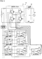
- Fig. 3 shows a configuration of the power converter 20 according to comparative example 2. A description of those features that are common to those of comparative example 1 will be omitted.
- positive and negative windings are provided from the third power supply circuit 23c to the second driver circuit 24b and the fourth driver circuit 24d individually. This increases the impedance of the wiring connecting the emitter terminal of the second switching device S2 and the emitter terminal of the fourth switching device S4 and so reduces the instantaneous current caused by a potential difference between the emitters. Further, the negative potentials of the second driver circuit 24b and the fourth driver circuit 24d can vary independently over a larger range.
- the emitter potential of the second switching device S2 and the negative potential of the second driver circuit 24b can match each other easily, and the emitter potential of the fourth switching device S4 and the negative potential of the fourth driver circuit 24d can match each other easily so that it is difficult for a false operation to occur.
- comparative example 2 requires more numerous wiring patterns so that the circuit scale is increased. If the substrate on which the third power supply circuit 23c is mounted and the substrate on which the second driver circuit 24b and the fourth driver circuit 24d are mounted are separate, the number of wirings across the substrates will be increased.
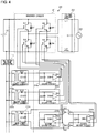
- Fig. 4 shows a configuration of the power converter 20 according to embodiment 1 of the present invention. A description of those features that are common to those of comparative example 1 will be omitted.
- the first switching device S1 ⁇ fourth switching device S4 and the first driver circuit 24a ⁇ fourth driver circuit 24d are mounted on the same substrate (hereinafter, referred to as the first substrate).
- the first switching device S1 ⁇ fourth switching device S4 and the first driver circuit 24a ⁇ fourth driver circuit 24d may be implemented in an Intelligent Power Module (IPM).
- IPM Intelligent Power Module
- the first power supply circuit 23a ⁇ third power supply circuit 23c are mounted on the second substrate separate from the first substrate. This permits a flexible arrangement such as stacking the second substrate on the first substrate in parallel or inserting the second substrate vertically. By employing such an arrangement, the vacant space in the housing of the power converter 20 is effectively used and the size of the housing of the power converter 20 is reduced.
- the wirings from the second substrate on which the third power supply circuit 23c is provided to the first substrate on which the second driver circuit 24b and the fourth driver circuit 24d are provided are used by the third power supply circuit 23c to supply the power supply voltage commonly to the second driver circuit 24b and the fourth driver circuit 24d.
- the second substrate on which the third power supply circuit 23c is provided is not individually wired to the second driver circuit 24b and to the fourth driver circuit 24d.
- a positive side branch node N1 of the positive side wiring from the third power supply circuit 23c and a negative side branch node N2 of the negative side wiring from the third power supply circuit 23c are formed in the first substrate.
- a first impedance device R1 is connected between the positive side branch node N1 and the positive side power supply terminal of the second driver circuit 24b.
- a second impedance device R2 is connected between the negative side branch node N2 and the negative side power supply terminal of the second driver circuit 24b.
- a third impedance device R3 is connected between the positive side branch node N1 and the positive side power supply terminal of the fourth driver circuit 24d.
- a fourth impedance device R4 is connected between the negative side branch node N2 and the negative side power supply terminal of the fourth driver circuit 24d.
- Each of the first impedance device R1 ⁇ fourth impedance device R4 may be a resistor or an inductor, or a combination thereof. The designer may select an optimal device as appropriate in accordance with experiments or simulations.
- the circuit scale and cost are reduced.
- two impedance devices are interposed between the emitter terminal of the second switching device S2 and the emitter terminal of the fourth switching device S4 so that the instantaneous current produced by a potential difference between the emitters is reduced.
- the negative potentials of the second driver circuit 24b and the fourth driver circuit 24d can vary independently over a larger range.
- the emitter potential of the second switching device S2 and the negative potential of the second driver circuit 24b can match each other easily, and the emitter potential of the fourth switching device S4 and the negative potential of the fourth driver circuit 24d can match each other easily so that it is difficult for a false operation to occur.
- the flexibility of arrangement of the substrates is increased. Further, by supplying electric power from the third power supply circuit 23c to the second driver circuit 24b and the fourth driver circuit 24d using common wirings, the number of wirings between the first substrate and the second substrate is prevented from increasing. This saves the mounting space of the power converter 20.
- Fig. 5 shows a configuration of the power converter 20 according to embodiment 2 of the present invention.
- the power converter 20 according to embodiment 2 is configured such that a clamp circuit 25, a fourth power supply circuit 23d, a fifth driver circuit 24e, and a sixth driver circuit 24f are added to the power converter 20 according to embodiment 1 shown in Fig. 4 .
- the clamp circuit 25 is connected between output lines P1 and P2 of the inverter circuit 21 and is capable of producing a short circuit between the output lines P1 and P2 of the inverter circuit 21 such that the direction of conduction in the short circuit is switchable.
- the inverter circuit 21 includes a fifth switching device S5 and a sixth switching device S6 connected in series.
- the collector terminal of the fifth switching device S5 is connected to the first output line of the inverter circuit 21
- the collector terminal of the sixth switching device S6 is connected to the second output line of the inverter circuit 21, and the emitter terminal of the fifth switching device S5 and the emitter terminal of the sixth switching device S6 are connected.
- a fifth feedback diode D5 is connected in parallel with the fifth switching device S5 in the direction in which a current flows from the emitter to the collector.
- a sixth feedback diode D6 is connected in parallel with the sixth switching device S6 in the direction in which a current flows from the emitter to the collector. Therefore, while the fifth switching device S5 is on and the sixth switching device S6 is off, a current flows only in the direction from the first output line to the second output line. While the fifth switching device S5 is off and the sixth switching device S6 is on, a current flows only in the direction from the second output line to the first output line.
- the fourth power supply circuit 23d subjects the reference voltage to DC-DC conversion so as to generate a power supply voltage common to the fifth driver circuit 24e and the sixth driver circuit 24f.
- the fourth power supply circuit 23d is configured similarly as the first power supply circuit 23a.
- the fifth driver circuit 24e generates a driving voltage to drive the fifth switching device S5 in accordance with a control signal CN5 for the fifth switching device S5.
- the sixth driver circuit 24f generates a driving voltage to drive the sixth switching device S6 in accordance with a control signal CN6 for the sixth switching device S6.
- the fifth driver circuit 24e and the sixth driver circuit 24f are configured similarly as the first driver circuit 24a.
- Fig. 6 shows an operation of the power converter 20 according to embodiment 2 of the present invention.
- PWM control is performed to cause the first switching device S1 and the fourth switching device S4 to be on and off repeatedly, the second switching device S2 and the fourth switching device S4 are controlled to be off, the fifth switching device S5 is controlled to be off, and the sixth switching device S6 is controlled to be on.
- PWM control is performed to cause the second switching device S2 and the third switching device S3 to be on and off repeatedly, the first switching device S1 and the fourth switching device S4 are controlled to be off, the fifth switching device S5 is controlled to be on, and the sixth switching device S6 is controlled to be off.
- a negative voltage -E is output to the filter circuit 22. While the second switching device S2 and the third switching device S3 are on, a negative voltage -E is output to the filter circuit 22. While the second switching device S2 and the third switching device S3 are off, the current based on the energy collected in the filter circuit 22 is fed back via the clamp circuit 25 so that the input voltage and the output voltage of the filter circuit 22 are brought to zero.
- the filter circuit 22 generates a sinusoidal wave (see the dotted line) based on the three levels including the positive voltage +E, zero, and the negative voltage -E.
- the first switching device S1 ⁇ sixth switching device S6 and the first driver circuit 24a ⁇ sixth driver circuit 24f are mounted on the first substrate and the first power supply circuit 23a ⁇ fourth power supply circuit 23d are mounted on the second substrate.
- the wirings from the second substrate on which the fourth power supply circuit 23d is provided to the first substrate on which the fifth driver circuit 24e and the sixth driver circuit 24f are provided are used by the fourth power supply circuit 23d to supply the power supply voltage commonly to the fifth driver circuit 24e and the sixth driver circuit 24f.
- a positive side branch node N3 of the positive side wiring from the fifth power supply circuit 23e and a negative side branch node N4 of the negative side wiring from the fifth power supply circuit 23e are formed in the first substrate.
- a fifth impedance device R5 is connected between the positive side branch node N3 and the positive side power supply terminal of the fifth driver circuit 24e.
- a sixth impedance device R6 is connected between the negative side branch node N4 and the negative side power supply terminal of the fifth driver circuit 24e.
- a seventh impedance device R7 is connected between the positive side branch node N3 and the positive side power supply terminal of the sixth driver circuit 24f.
- An eighth impedance device R8 is connected between the negative side branch node N4 and the negative side power supply terminal of the sixth driver circuit 24f.
- embodiment 2 provides the same advantage as embodiment 1.
- the output waveform is configured to be closer to a sinusoidal wave by forming a 3-level inverter by adding the clamp circuit 25. Accordingly, the size of the filter circuit 22 for producing a sinusoidal output waveform is reduced. Still further, the voltage amplitude occurring when the first switching device S1 ⁇ fourth switching device S4 are switched is reduced to half as compared to the case of the 2-level inverter so that the switching loss is substantially reduced to half. Accordingly, the conversion efficiency is improved and the noise generated from the power converter 20 is also reduced.
- the circuit scale and cost are reduced. Still further, by providing the positive side branch node N3, the negative side branch node N4, and the fifth impedance device R5 ⁇ eighth impedance device R8 on the first substrate, a false operation of the fifth switching device S5 and the sixth switching device S6 is prevented, while also preventing the number of wirings between the first substrate and the second substrate from increasing.
- Fig. 7 shows a configuration of the power converter 20 according to embodiment 3 of the present invention.
- the power converter 20 according to embodiment 3 is configured such that a clamp circuit 25, a fifth driver circuit 24e, and a sixth driver circuit 24f are added to the power converter 20 according to embodiment 1 shown in Fig. 4 .
- the clamp circuit 25 is connected between output lines P1 and P2 of the inverter circuit 21 and is capable of producing a short circuit between the output lines P1 and P2 of the inverter circuit 21 such that the direction of conduction in the short circuit is switchable.
- the inverter circuit 21 includes a fifth switching device S5 and a sixth switching device S6 connected in series.
- the directions of the fifth switching device S5 and the sixth switching device S6 are opposite to those of embodiment 2.
- the emitter terminal of the fifth switching device S5 is connected to the first output line of the inverter circuit 21
- the emitter terminal of the sixth switching device S6 is connected to the second output line of the inverter circuit 21, and the collector terminal of the fifth switching device S5 and the collector terminal of the sixth switching device S6 are connected.
- a fifth feedback diode D5 is connected in parallel with the fifth switching device S5 in the direction in which a current flows from the emitter to the collector.
- a sixth feedback diode D6 is connected in parallel with the sixth switching device S6 in the direction in which a current flows from the emitter to the collector. Therefore, while the fifth switching device S5 is on and the sixth switching device is off, a current flows only in the direction from the second output line to the first output line. While the fifth switching device S5 is off and the sixth switching device S6 is on, a current flows only in the direction from the first output line to the second output line.
- the first power supply circuit 23a subjects the reference voltage to DC-DC conversion so as to generate a power supply voltage common to the first driver circuit 24a and the fifth driver circuit 24e.
- the second power supply circuit 23b subjects the reference voltage to DC-DC conversion so as to generate a power supply voltage common to the third driver circuit 24c and the sixth driver circuit 24f.
- the operation of the power converter 20 according to embodiment 3 is the same as the operation of the power converter 20 according to embodiment 2 shown in Fig. 6 except that the fifth switching device S5 and the sixth switching device S6 are turned on/off on opposite conditions.
- the first switching device S1 ⁇ sixth switching device S6 and the first driver circuit 24a ⁇ sixth driver circuit 24f are mounted on the first substrate and the first power supply circuit 23a ⁇ third power supply circuit 23c are mounted on the second substrate.
- the wirings from the second substrate on which the first power supply circuit 23a is provided to the first substrate on which the first driver circuit 24a and the fifth driver circuit 24e are provided are used by the first power supply circuit 23a to supply the power supply voltage commonly to the first driver circuit 24a and the fifth driver circuit 24e.
- a positive side branch node N5 of the positive side wiring from the first power supply circuit 23a and a negative side branch node N6 of the negative side wiring from the first power supply circuit 23a are formed in the first substrate.
- a ninth impedance device R9 is connected between the positive side branch node N5 and the positive side power supply terminal of the first driver circuit 24a.
- a tenth impedance device R10 is connected between the negative side branch node N6 and the negative side power supply terminal of the first driver circuit 24a.
- An eleventh impedance device R11 is connected between the positive side branch node N5 and the positive side power supply terminal of the fifth driver circuit 24e.
- a twelfth impedance device R12 is connected between the negative side branch node N6 and the negative side power supply terminal of the fifth driver circuit 24e.
- the wirings from the second substrate on which the second power supply circuit 23b is provided to the first substrate on which the third driver circuit 24c and the sixth driver circuit 24f are provided are used by the second power supply circuit 23b to supply the power supply voltage commonly to the third driver circuit 24c and the sixth driver circuit 24f.
- a positive side branch node N7 of the positive side wiring from the second power supply circuit 23b and a negative side branch node N8 of the negative side wiring from the second power supply circuit 23b are formed in the first substrate.
- a thirteenth impedance device R13 is connected between the positive side branch node N7 and the positive side power supply terminal of the third driver circuit 24c.
- a fourteenth impedance device R14 is connected between the negative side branch node N8 and the negative side power supply terminal of the third driver circuit 24c.
- a fifteenth impedance device R15 is connected between the positive side branch node N7 and the positive side power supply terminal of the sixth driver circuit 24f.
- An sixteenth impedance device R16 is connected between the negative side branch node N8 and the negative side power supply terminal of the sixth driver circuit 24f.
- embodiment 3 provides the same advantage as embodiment 2.
- the emitter terminal of the first switching device S1 and the emitter terminal of the fifth switching device S5 are connected by a high current path
- the emitter terminal of the third switching device S3 and the emitter terminal of the sixth switching device S6 are connected by a high current path. Therefore, a potential difference larger than the potential difference between the emitter terminal of the fifth switching device S5 and the emitter terminal of the sixth switching device S6 according embodiment 2 tends to be produced but the impact from this potential difference is mitigated by providing the ninth impedance device R9 ⁇ sixteenth impedance device R16.
- an inverter circuit 21 for converting a DC power into a single-phase AC power is assumed.
- the inventive technology can also be applied to an inverter circuit for converting a DC power into a three-phase AC power.
- a common power supply circuit is used for the three driver circuits that drive the three switching devices on the lower side.
- the positive side branch node provided in the first substrate is connected to the positive side power supply terminal of the three driver circuits via respective impedance devices, and the negative side branch node is connected to the negative side power supply terminal of the three driver circuits via respective impedance devices.
- the embodiments may be defined by the following items.
- a power converter (20) comprising:
- a common power supply circuit is used for the second driver circuit (24b) for the second switching device (S2) and the second driver circuit (24b) for the fourth switching device (S4), while also inhibiting a false operation of the second switching device (S2) and the fourth switching device (S4).
- the power supply voltage for the second driver circuit (24b) and the fourth driver circuit (24d) can be generated from the reference voltage while also securing insulation.
- a common power supply circuit is used for the fifth driver circuit (24e) for the fifth switching device (S5) forming the three-level clamp circuit (25) and for the sixth driver circuit (24f) for the sixth switching device (S6) also forming the three-level clamp circuit (25), while also inhibiting a false operation of the fifth switching device (S5) and the sixth switching device (S6) .
- the present invention can be used for power conditioners of solar cells, etc.
Landscapes
- Engineering & Computer Science (AREA)
- Power Engineering (AREA)
- Inverter Devices (AREA)
- Power Conversion In General (AREA)
- Supply And Distribution Of Alternating Current (AREA)
Applications Claiming Priority (2)
| Application Number | Priority Date | Filing Date | Title |
|---|---|---|---|
| JP2015169197A JP6555521B2 (ja) | 2015-08-28 | 2015-08-28 | 電力変換装置 |
| PCT/JP2016/003690 WO2017038022A1 (ja) | 2015-08-28 | 2016-08-10 | 電力変換装置 |
Publications (2)
| Publication Number | Publication Date |
|---|---|
| EP3343748A1 true EP3343748A1 (de) | 2018-07-04 |
| EP3343748A4 EP3343748A4 (de) | 2018-07-11 |
Family
ID=58186820
Family Applications (1)
| Application Number | Title | Priority Date | Filing Date |
|---|---|---|---|
| EP16841063.7A Withdrawn EP3343748A4 (de) | 2015-08-28 | 2016-08-10 | Stromwandlungsvorrichtung |
Country Status (6)
| Country | Link |
|---|---|
| US (1) | US10135360B2 (de) |
| EP (1) | EP3343748A4 (de) |
| JP (1) | JP6555521B2 (de) |
| AU (1) | AU2016314916B2 (de) |
| NZ (1) | NZ738567A (de) |
| WO (1) | WO2017038022A1 (de) |
Families Citing this family (10)
| Publication number | Priority date | Publication date | Assignee | Title |
|---|---|---|---|---|
| US12395068B2 (en) | 2017-03-29 | 2025-08-19 | Solaredge Technologies Ltd. | Bypass circuit and method to bypass power modules in power system |
| JP6755212B2 (ja) * | 2017-03-24 | 2020-09-16 | 株式会社豊田中央研究所 | スイッチ回路 |
| CN108695843B (zh) | 2017-03-29 | 2023-09-22 | 太阳能安吉科技有限公司 | 旁路电路和在电力系统中旁通电力模块的方法 |
| WO2019097835A1 (ja) * | 2017-11-14 | 2019-05-23 | 三菱電機株式会社 | 電力変換装置 |
| JP2019170033A (ja) * | 2018-03-22 | 2019-10-03 | パナソニックIpマネジメント株式会社 | 電力変換装置 |
| US11139746B2 (en) * | 2019-01-31 | 2021-10-05 | Rockwell Automation Technologies, Inc. | Power converter with reduced switch mode power supply EMI |
| JP6647471B1 (ja) * | 2019-07-04 | 2020-02-14 | 三菱電機株式会社 | 3レベル電力変換装置 |
| US11699961B2 (en) * | 2019-07-04 | 2023-07-11 | Mitsubishi Electric Corporation | Three-level power conversion device |
| JP7725331B2 (ja) * | 2021-10-19 | 2025-08-19 | 愛三工業株式会社 | 電動車両用パワーコントロールユニット |
| JP7254159B1 (ja) * | 2021-12-24 | 2023-04-07 | 三菱電機株式会社 | 電力変換装置 |
Family Cites Families (13)
| Publication number | Priority date | Publication date | Assignee | Title |
|---|---|---|---|---|
| JP3919624B2 (ja) * | 2002-07-24 | 2007-05-30 | 三菱電機株式会社 | パワーデバイス駆動回路 |
| JP2004201480A (ja) * | 2002-12-20 | 2004-07-15 | Honda Motor Co Ltd | インバータ制御式発電装置 |
| JP4847707B2 (ja) | 2005-03-10 | 2011-12-28 | 三菱電機株式会社 | 電力用半導体装置 |
| JP2006271041A (ja) * | 2005-03-23 | 2006-10-05 | Fuji Electric Holdings Co Ltd | 電圧駆動型半導体素子のゲート駆動装置 |
| JP5317413B2 (ja) * | 2007-02-06 | 2013-10-16 | 株式会社東芝 | 半導体スイッチおよび当該半導体スイッチを適用した電力変換装置 |
| US8476859B2 (en) * | 2010-09-30 | 2013-07-02 | Rockwell Automation Technologies, Inc. | DC power for SGCT devices using a high frequency current loop with multiple current transformers |
| JP5433608B2 (ja) * | 2011-03-03 | 2014-03-05 | 日立オートモティブシステムズ株式会社 | 電力変換装置 |
| JP5236822B1 (ja) * | 2012-01-30 | 2013-07-17 | シャープ株式会社 | ドライバ回路 |
| JP6136011B2 (ja) * | 2013-08-02 | 2017-05-31 | パナソニックIpマネジメント株式会社 | 半導体装置、および電力変換装置 |
| JP6094444B2 (ja) * | 2013-10-04 | 2017-03-15 | 株式会社デンソー | 絶縁電源装置 |
| WO2015053142A1 (ja) * | 2013-10-09 | 2015-04-16 | 日立オートモティブシステムズ株式会社 | ドライバ基板および電力変換装置 |
| CN105765847B (zh) * | 2013-11-29 | 2018-12-25 | 新电元工业株式会社 | 逆变器装置 |
| JP6191478B2 (ja) * | 2014-01-28 | 2017-09-06 | アイシン・エィ・ダブリュ株式会社 | 電力変換装置 |
-
2015
- 2015-08-28 JP JP2015169197A patent/JP6555521B2/ja active Active
-
2016
- 2016-08-10 WO PCT/JP2016/003690 patent/WO2017038022A1/ja not_active Ceased
- 2016-08-10 AU AU2016314916A patent/AU2016314916B2/en not_active Ceased
- 2016-08-10 NZ NZ73856716A patent/NZ738567A/en not_active IP Right Cessation
- 2016-08-10 EP EP16841063.7A patent/EP3343748A4/de not_active Withdrawn
-
2018
- 2018-01-12 US US15/870,465 patent/US10135360B2/en active Active
Also Published As
| Publication number | Publication date |
|---|---|
| AU2016314916B2 (en) | 2019-01-24 |
| NZ738567A (en) | 2019-09-27 |
| US10135360B2 (en) | 2018-11-20 |
| JP2017046531A (ja) | 2017-03-02 |
| JP6555521B2 (ja) | 2019-08-07 |
| AU2016314916A1 (en) | 2018-01-18 |
| WO2017038022A1 (ja) | 2017-03-09 |
| EP3343748A4 (de) | 2018-07-11 |
| US20180138827A1 (en) | 2018-05-17 |
Similar Documents
| Publication | Publication Date | Title |
|---|---|---|
| AU2016314916B2 (en) | Power conversion device | |
| US8385092B1 (en) | Power converter with current vector controlled dead time | |
| US8861235B2 (en) | Power converting apparatus | |
| US8848405B2 (en) | Highly efficient half-bridge DC-AC converter | |
| US9979322B2 (en) | Modulator for a hybrid converter system | |
| JP6206502B2 (ja) | 電力変換装置及び電力変換方法 | |
| EP3934090A1 (de) | Hybrides wandlersystem | |
| US10581342B2 (en) | Three-level two-stage decoupled active NPC converter | |
| EP2698911B1 (de) | Elektronischer stromkreis | |
| US11070163B2 (en) | Driving power supply device | |
| EP2410648A1 (de) | Gleichstromwandlerschaltung und Verfahren zur Steuerung einer Gleichstromwandlerschaltung | |
| CN107787548A (zh) | 充电共用逆变器 | |
| CN111231692A (zh) | 具有在栅极驱动器处生成的增强共源极电感的逆变器系统 | |
| JPWO2018043367A1 (ja) | 電力変換システム | |
| WO2015015721A1 (ja) | 半導体装置、および電力変換装置 | |
| JP4873317B2 (ja) | インバータ装置 | |
| US11165359B2 (en) | Power conversion system configured to perform power conversion between direct current and three-phase alternating current | |
| CN203827171U (zh) | 电力负载的驱动电路 | |
| KR20210108369A (ko) | 3-레벨 ANPC(Active Neutral-Point-Clamped) 하이브리드 컨버터 | |
| US11990826B2 (en) | Power electronics device and method for supplying electrical voltage to a driver circuit of a power semiconductor switch | |
| KR20130088606A (ko) | 3-레벨 인버터 제어 장치와, 3-레벨 인버터를 구비한 전원 공급 장치 및 모터 구동 장치 | |
| EP3086458B1 (de) | Wechselrichterschaltung und verfahren zur herstellung der wechselrichterschaltung | |
| US10998809B2 (en) | Power conversion apparatus | |
| US10848049B2 (en) | Main conversion circuit, power conversion device, and moving body | |
| CN222366189U (zh) | 一种多级并联源极驱动变换器电路及开关电源 |
Legal Events
| Date | Code | Title | Description |
|---|---|---|---|
| PUAI | Public reference made under article 153(3) epc to a published international application that has entered the european phase |
Free format text: ORIGINAL CODE: 0009012 |
|
| 17P | Request for examination filed |
Effective date: 20171219 |
|
| AK | Designated contracting states |
Kind code of ref document: A1 Designated state(s): AL AT BE BG CH CY CZ DE DK EE ES FI FR GB GR HR HU IE IS IT LI LT LU LV MC MK MT NL NO PL PT RO RS SE SI SK SM TR |
|
| AX | Request for extension of the european patent |
Extension state: BA ME |
|
| A4 | Supplementary search report drawn up and despatched |
Effective date: 20180607 |
|
| RIC1 | Information provided on ipc code assigned before grant |
Ipc: H03K 17/082 20060101ALI20180601BHEP Ipc: H02M 7/5387 20070101ALI20180601BHEP Ipc: H03K 17/16 20060101ALI20180601BHEP Ipc: H02M 1/12 20060101ALN20180601BHEP Ipc: H02M 1/08 20060101ALI20180601BHEP Ipc: H02M 1/38 20070101AFI20180601BHEP Ipc: H02M 1/00 20060101ALN20180601BHEP |
|
| DAV | Request for validation of the european patent (deleted) | ||
| DAX | Request for extension of the european patent (deleted) | ||
| 17Q | First examination report despatched |
Effective date: 20190426 |
|
| STAA | Information on the status of an ep patent application or granted ep patent |
Free format text: STATUS: THE APPLICATION HAS BEEN WITHDRAWN |
|
| 18W | Application withdrawn |
Effective date: 20190605 |