EP3346337B1 - Optische verarbeitungsvorrichtung, beschichtungs-/entwicklungsvorrichtung, optisches verarbeitungsverfahren und nicht transitorisches computerlesbares speichermedium - Google Patents
Optische verarbeitungsvorrichtung, beschichtungs-/entwicklungsvorrichtung, optisches verarbeitungsverfahren und nicht transitorisches computerlesbares speichermedium Download PDFInfo
- Publication number
- EP3346337B1 EP3346337B1 EP17207286.0A EP17207286A EP3346337B1 EP 3346337 B1 EP3346337 B1 EP 3346337B1 EP 17207286 A EP17207286 A EP 17207286A EP 3346337 B1 EP3346337 B1 EP 3346337B1
- Authority
- EP
- European Patent Office
- Prior art keywords
- light
- illuminance
- distribution pattern
- illuminance distribution
- unit
- Prior art date
- Legal status (The legal status is an assumption and is not a legal conclusion. Google has not performed a legal analysis and makes no representation as to the accuracy of the status listed.)
- Active
Links
Images





Classifications
-
- G—PHYSICS
- G03—PHOTOGRAPHY; CINEMATOGRAPHY; ANALOGOUS TECHNIQUES USING WAVES OTHER THAN OPTICAL WAVES; ELECTROGRAPHY; HOLOGRAPHY
- G03F—PHOTOMECHANICAL PRODUCTION OF TEXTURED OR PATTERNED SURFACES, e.g. FOR PRINTING, FOR PROCESSING OF SEMICONDUCTOR DEVICES; MATERIALS THEREFOR; ORIGINALS THEREFOR; APPARATUS SPECIALLY ADAPTED THEREFOR
- G03F7/00—Photomechanical, e.g. photolithographic, production of textured or patterned surfaces, e.g. printing surfaces; Materials therefor, e.g. comprising photoresists; Apparatus specially adapted therefor
- G03F7/70—Microphotolithographic exposure; Apparatus therefor
- G03F7/70483—Information management; Active and passive control; Testing; Wafer monitoring, e.g. pattern monitoring
- G03F7/7055—Exposure light control in all parts of the microlithographic apparatus, e.g. pulse length control or light interruption
-
- G—PHYSICS
- G03—PHOTOGRAPHY; CINEMATOGRAPHY; ANALOGOUS TECHNIQUES USING WAVES OTHER THAN OPTICAL WAVES; ELECTROGRAPHY; HOLOGRAPHY
- G03F—PHOTOMECHANICAL PRODUCTION OF TEXTURED OR PATTERNED SURFACES, e.g. FOR PRINTING, FOR PROCESSING OF SEMICONDUCTOR DEVICES; MATERIALS THEREFOR; ORIGINALS THEREFOR; APPARATUS SPECIALLY ADAPTED THEREFOR
- G03F7/00—Photomechanical, e.g. photolithographic, production of textured or patterned surfaces, e.g. printing surfaces; Materials therefor, e.g. comprising photoresists; Apparatus specially adapted therefor
- G03F7/20—Exposure; Apparatus therefor
- G03F7/2002—Exposure; Apparatus therefor with visible light or UV light, through an original having an opaque pattern on a transparent support, e.g. film printing, projection printing; by reflection of visible or UV light from an original such as a printed image
- G03F7/2004—Exposure; Apparatus therefor with visible light or UV light, through an original having an opaque pattern on a transparent support, e.g. film printing, projection printing; by reflection of visible or UV light from an original such as a printed image characterised by the use of a particular light source, e.g. fluorescent lamps or deep UV light
-
- G—PHYSICS
- G03—PHOTOGRAPHY; CINEMATOGRAPHY; ANALOGOUS TECHNIQUES USING WAVES OTHER THAN OPTICAL WAVES; ELECTROGRAPHY; HOLOGRAPHY
- G03F—PHOTOMECHANICAL PRODUCTION OF TEXTURED OR PATTERNED SURFACES, e.g. FOR PRINTING, FOR PROCESSING OF SEMICONDUCTOR DEVICES; MATERIALS THEREFOR; ORIGINALS THEREFOR; APPARATUS SPECIALLY ADAPTED THEREFOR
- G03F7/00—Photomechanical, e.g. photolithographic, production of textured or patterned surfaces, e.g. printing surfaces; Materials therefor, e.g. comprising photoresists; Apparatus specially adapted therefor
- G03F7/16—Coating processes; Apparatus therefor
-
- G—PHYSICS
- G03—PHOTOGRAPHY; CINEMATOGRAPHY; ANALOGOUS TECHNIQUES USING WAVES OTHER THAN OPTICAL WAVES; ELECTROGRAPHY; HOLOGRAPHY
- G03F—PHOTOMECHANICAL PRODUCTION OF TEXTURED OR PATTERNED SURFACES, e.g. FOR PRINTING, FOR PROCESSING OF SEMICONDUCTOR DEVICES; MATERIALS THEREFOR; ORIGINALS THEREFOR; APPARATUS SPECIALLY ADAPTED THEREFOR
- G03F7/00—Photomechanical, e.g. photolithographic, production of textured or patterned surfaces, e.g. printing surfaces; Materials therefor, e.g. comprising photoresists; Apparatus specially adapted therefor
- G03F7/20—Exposure; Apparatus therefor
- G03F7/2022—Multi-step exposure, e.g. hybrid; backside exposure; blanket exposure, e.g. for image reversal; edge exposure, e.g. for edge bead removal; corrective exposure
-
- G—PHYSICS
- G03—PHOTOGRAPHY; CINEMATOGRAPHY; ANALOGOUS TECHNIQUES USING WAVES OTHER THAN OPTICAL WAVES; ELECTROGRAPHY; HOLOGRAPHY
- G03F—PHOTOMECHANICAL PRODUCTION OF TEXTURED OR PATTERNED SURFACES, e.g. FOR PRINTING, FOR PROCESSING OF SEMICONDUCTOR DEVICES; MATERIALS THEREFOR; ORIGINALS THEREFOR; APPARATUS SPECIALLY ADAPTED THEREFOR
- G03F7/00—Photomechanical, e.g. photolithographic, production of textured or patterned surfaces, e.g. printing surfaces; Materials therefor, e.g. comprising photoresists; Apparatus specially adapted therefor
- G03F7/26—Processing photosensitive materials; Apparatus therefor
- G03F7/30—Imagewise removal using liquid means
-
- G—PHYSICS
- G03—PHOTOGRAPHY; CINEMATOGRAPHY; ANALOGOUS TECHNIQUES USING WAVES OTHER THAN OPTICAL WAVES; ELECTROGRAPHY; HOLOGRAPHY
- G03F—PHOTOMECHANICAL PRODUCTION OF TEXTURED OR PATTERNED SURFACES, e.g. FOR PRINTING, FOR PROCESSING OF SEMICONDUCTOR DEVICES; MATERIALS THEREFOR; ORIGINALS THEREFOR; APPARATUS SPECIALLY ADAPTED THEREFOR
- G03F7/00—Photomechanical, e.g. photolithographic, production of textured or patterned surfaces, e.g. printing surfaces; Materials therefor, e.g. comprising photoresists; Apparatus specially adapted therefor
- G03F7/70—Microphotolithographic exposure; Apparatus therefor
- G03F7/70008—Production of exposure light, i.e. light sources
- G03F7/7005—Production of exposure light, i.e. light sources by multiple sources, e.g. light-emitting diodes [LED] or light source arrays
-
- G—PHYSICS
- G03—PHOTOGRAPHY; CINEMATOGRAPHY; ANALOGOUS TECHNIQUES USING WAVES OTHER THAN OPTICAL WAVES; ELECTROGRAPHY; HOLOGRAPHY
- G03F—PHOTOMECHANICAL PRODUCTION OF TEXTURED OR PATTERNED SURFACES, e.g. FOR PRINTING, FOR PROCESSING OF SEMICONDUCTOR DEVICES; MATERIALS THEREFOR; ORIGINALS THEREFOR; APPARATUS SPECIALLY ADAPTED THEREFOR
- G03F7/00—Photomechanical, e.g. photolithographic, production of textured or patterned surfaces, e.g. printing surfaces; Materials therefor, e.g. comprising photoresists; Apparatus specially adapted therefor
- G03F7/70—Microphotolithographic exposure; Apparatus therefor
- G03F7/70058—Mask illumination systems
- G03F7/70133—Measurement of illumination distribution, in pupil plane or field plane
-
- G—PHYSICS
- G03—PHOTOGRAPHY; CINEMATOGRAPHY; ANALOGOUS TECHNIQUES USING WAVES OTHER THAN OPTICAL WAVES; ELECTROGRAPHY; HOLOGRAPHY
- G03F—PHOTOMECHANICAL PRODUCTION OF TEXTURED OR PATTERNED SURFACES, e.g. FOR PRINTING, FOR PROCESSING OF SEMICONDUCTOR DEVICES; MATERIALS THEREFOR; ORIGINALS THEREFOR; APPARATUS SPECIALLY ADAPTED THEREFOR
- G03F7/00—Photomechanical, e.g. photolithographic, production of textured or patterned surfaces, e.g. printing surfaces; Materials therefor, e.g. comprising photoresists; Apparatus specially adapted therefor
- G03F7/70—Microphotolithographic exposure; Apparatus therefor
- G03F7/70383—Direct write, i.e. pattern is written directly without the use of a mask by one or multiple beams
- G03F7/70391—Addressable array sources specially adapted to produce patterns, e.g. addressable LED arrays
-
- G—PHYSICS
- G03—PHOTOGRAPHY; CINEMATOGRAPHY; ANALOGOUS TECHNIQUES USING WAVES OTHER THAN OPTICAL WAVES; ELECTROGRAPHY; HOLOGRAPHY
- G03F—PHOTOMECHANICAL PRODUCTION OF TEXTURED OR PATTERNED SURFACES, e.g. FOR PRINTING, FOR PROCESSING OF SEMICONDUCTOR DEVICES; MATERIALS THEREFOR; ORIGINALS THEREFOR; APPARATUS SPECIALLY ADAPTED THEREFOR
- G03F7/00—Photomechanical, e.g. photolithographic, production of textured or patterned surfaces, e.g. printing surfaces; Materials therefor, e.g. comprising photoresists; Apparatus specially adapted therefor
- G03F7/70—Microphotolithographic exposure; Apparatus therefor
- G03F7/70483—Information management; Active and passive control; Testing; Wafer monitoring, e.g. pattern monitoring
- G03F7/7055—Exposure light control in all parts of the microlithographic apparatus, e.g. pulse length control or light interruption
- G03F7/70558—Dose control, i.e. achievement of a desired dose
-
- G—PHYSICS
- G03—PHOTOGRAPHY; CINEMATOGRAPHY; ANALOGOUS TECHNIQUES USING WAVES OTHER THAN OPTICAL WAVES; ELECTROGRAPHY; HOLOGRAPHY
- G03F—PHOTOMECHANICAL PRODUCTION OF TEXTURED OR PATTERNED SURFACES, e.g. FOR PRINTING, FOR PROCESSING OF SEMICONDUCTOR DEVICES; MATERIALS THEREFOR; ORIGINALS THEREFOR; APPARATUS SPECIALLY ADAPTED THEREFOR
- G03F7/00—Photomechanical, e.g. photolithographic, production of textured or patterned surfaces, e.g. printing surfaces; Materials therefor, e.g. comprising photoresists; Apparatus specially adapted therefor
- G03F7/70—Microphotolithographic exposure; Apparatus therefor
- G03F7/70483—Information management; Active and passive control; Testing; Wafer monitoring, e.g. pattern monitoring
- G03F7/70591—Testing optical components
-
- G—PHYSICS
- G03—PHOTOGRAPHY; CINEMATOGRAPHY; ANALOGOUS TECHNIQUES USING WAVES OTHER THAN OPTICAL WAVES; ELECTROGRAPHY; HOLOGRAPHY
- G03F—PHOTOMECHANICAL PRODUCTION OF TEXTURED OR PATTERNED SURFACES, e.g. FOR PRINTING, FOR PROCESSING OF SEMICONDUCTOR DEVICES; MATERIALS THEREFOR; ORIGINALS THEREFOR; APPARATUS SPECIALLY ADAPTED THEREFOR
- G03F7/00—Photomechanical, e.g. photolithographic, production of textured or patterned surfaces, e.g. printing surfaces; Materials therefor, e.g. comprising photoresists; Apparatus specially adapted therefor
- G03F7/70—Microphotolithographic exposure; Apparatus therefor
- G03F7/70691—Handling of masks or workpieces
-
- H—ELECTRICITY
- H10—SEMICONDUCTOR DEVICES; ELECTRIC SOLID-STATE DEVICES NOT OTHERWISE PROVIDED FOR
- H10P—GENERIC PROCESSES OR APPARATUS FOR THE MANUFACTURE OR TREATMENT OF DEVICES COVERED BY CLASS H10
- H10P72/00—Handling or holding of wafers, substrates or devices during manufacture or treatment thereof
- H10P72/04—Apparatus for manufacture or treatment
- H10P72/0431—Apparatus for thermal treatment
- H10P72/0436—Apparatus for thermal treatment mainly by radiation
-
- H—ELECTRICITY
- H10—SEMICONDUCTOR DEVICES; ELECTRIC SOLID-STATE DEVICES NOT OTHERWISE PROVIDED FOR
- H10P—GENERIC PROCESSES OR APPARATUS FOR THE MANUFACTURE OR TREATMENT OF DEVICES COVERED BY CLASS H10
- H10P72/00—Handling or holding of wafers, substrates or devices during manufacture or treatment thereof
- H10P72/04—Apparatus for manufacture or treatment
- H10P72/0448—Apparatus for applying a liquid, a resin, an ink or the like
-
- H—ELECTRICITY
- H10—SEMICONDUCTOR DEVICES; ELECTRIC SOLID-STATE DEVICES NOT OTHERWISE PROVIDED FOR
- H10P—GENERIC PROCESSES OR APPARATUS FOR THE MANUFACTURE OR TREATMENT OF DEVICES COVERED BY CLASS H10
- H10P76/00—Manufacture or treatment of masks on semiconductor bodies, e.g. by lithography or photolithography
-
- G—PHYSICS
- G03—PHOTOGRAPHY; CINEMATOGRAPHY; ANALOGOUS TECHNIQUES USING WAVES OTHER THAN OPTICAL WAVES; ELECTROGRAPHY; HOLOGRAPHY
- G03F—PHOTOMECHANICAL PRODUCTION OF TEXTURED OR PATTERNED SURFACES, e.g. FOR PRINTING, FOR PROCESSING OF SEMICONDUCTOR DEVICES; MATERIALS THEREFOR; ORIGINALS THEREFOR; APPARATUS SPECIALLY ADAPTED THEREFOR
- G03F7/00—Photomechanical, e.g. photolithographic, production of textured or patterned surfaces, e.g. printing surfaces; Materials therefor, e.g. comprising photoresists; Apparatus specially adapted therefor
- G03F7/20—Exposure; Apparatus therefor
- G03F7/2002—Exposure; Apparatus therefor with visible light or UV light, through an original having an opaque pattern on a transparent support, e.g. film printing, projection printing; by reflection of visible or UV light from an original such as a printed image
- G03F7/201—Exposure; Apparatus therefor with visible light or UV light, through an original having an opaque pattern on a transparent support, e.g. film printing, projection printing; by reflection of visible or UV light from an original such as a printed image characterised by an oblique exposure; characterised by the use of plural sources; characterised by the rotation of the optical device; characterised by a relative movement of the optical device, the light source, the sensitive system or the mask
Definitions
- the present invention relates to a technology for processing a surface of a workpiece by irradiating the surface with light.
- EUV extreme-ultraviolet
- Japanese patent application publication No. 2015-156472 discloses an exposure apparatus that improves in-plane uniformity of line width of a pattern (circuit pattern) on a semiconductor wafer (hereinafter referred to simply as a "wafer") by performing pattern exposure on the wafer, coated with a resist of the photosensitization chemical amplification type, by use of a pattern mask and thereafter further performing batch exposure on pattern-exposed regions.
- This so-called batch exposure apparatus uses a light-emitting diode (LED) as the light source and performs exposure on the whole surface of the wafer by forming a strip-shaped irradiation region, slightly longer than the wafer's diameter, on the wafer and moving the wafer in a direction orthogonal to the extending direction of the irradiation region.
- LED light-emitting diode
- the present invention has been made under the above-described circumstances, and an object of the present invention is to provide a technology capable of easily adjusting an illuminance distribution pattern in the irradiation region in the lengthwise direction to a target illuminance distribution pattern with high accuracy when optical processing is performed on a workpiece by forming a strip-shaped irradiation region with a light source unit in which a plurality of light-emitting blocks, each formed of one or more light-emitting diodes, are linearly arranged.
- An optical processing apparatus includes:
- Another invention is a coating/development apparatus including a module for forming a resist film on a substrate by using a coating liquid, a module for developing the substrate (W) after pattern exposure, a transfer mechanism for transferring the substrate between the modules, and the optical processing apparatus according to the present invention.
- Still another invention is an optical processing method for processing a workpiece with light, in which: the optical processing method uses:
- Yet another invention is a non-transitory computer-readable storage medium storing a computer program to be used for an apparatus that performs processing on a workpiece by irradiating the workpiece with light and includes:
- the change amount (response) of the illuminance distribution pattern (illuminance profile), associating the position in the irradiation region in the lengthwise direction with the change amount of the illuminance with respect to the change in the current (drive current), has previously been acquired for each light-emitting block.
- the illuminance distribution pattern of each light-emitting block is obtained by using the change amount of the illuminance distribution pattern (the term "illuminance distribution response amount" is used in the description of the embodiment), and the illuminance distribution pattern of all the light-emitting blocks in the lengthwise direction is estimated by obtaining the sum of the illuminance distribution patterns of the light-emitting blocks.
- the illuminance distribution pattern in the lengthwise direction of the irradiation region can be adjusted to the target illuminance distribution pattern with ease and with high accuracy, and difference in the illuminance distribution pattern among apparatuses (i.e., among a plurality of optical processing apparatuses) can be kept down.
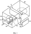
- Fig. 1 is an external view (perspective view) of an optical processing apparatus according to an embodiment of the present invention.
- the optical processing apparatus comprises a housing 30 with a carry-in/carry-out port 31 formed on the front side.
- the housing 30 is drawn transparently to make the inside of the housing 30 visible.
- a mount 32 on which a wafer W, as a workpiece that will undergo optical processing such as exposure, can be set is provided on the base of the housing 30.
- the mount 32 can be moved freely along a guide rail 33 extending from a handover position (position shown in Fig. 1 ) for a wafer W on the side of the carry-in/carry-out port 31 to a standby position on the far side of the housing 30.
- the mount 32 is connected, via a rotary shaft, to a drive unit 34 for rotating a wafer W set on the mount 32 around the vertical axis.
- the drive unit 34 is described as a combination of a motor which rotates the mount 32 and a moving mechanism which holds the motor and moves along the guide rail 33.
- a well-known positioning mechanism (mechanism including a light-emitting unit and a photoreceptor unit vertically facing each other across the circumferential part of the wafer W), which is not illustrated in the drawings, is provided.
- the positioning mechanism detects the orientation of a notch serving as a positioning part formed on the circumference of the wafer W and performs control so that the orientation of the wafer W undergoing the exposure process is kept constant by the rotation of the mount 32 by the drive unit 34.
- An optical irradiation unit 4 for irradiating the wafer W with ultraviolet rays is provided above a position between the handover position for a wafer W and the aforementioned standby position in a wafer W movement region in which the wafer W moves.
- the optical irradiation unit 4 has a rectangular case body 40 wider in a transverse direction than the width of the wafer W movement region as shown in Figs. 1 and 2 .
- an LED light source set 400 serving as a light source unit is provided inside the case body 40.
- the LED light source set 400 is formed by arranging a plurality of light-emitting blocks 42, e.g., eighty-eight (88) light-emitting blocks 42, in the transverse direction.
- Each light-emitting block 42 is formed of a plurality of LEDs 41, e.g., four (4) LEDs 41, arranged in the longitudinal direction.
- the LED arrangement is simplified and a smaller number of LEDs are drawn for convenience to avoid difficulty in drawing the figures and to put a high priority on easy understanding of the structure.
- the LED light source set 400 is fixed to a common LED substrate 43 provided in the case body 40 and is arranged so as to emit ultraviolet rays downward.
- a slit 44 serving as an irradiation hole extending in the transverse direction and longer than the width of the movement region for a wafer W in the transverse direction is formed through the base of the case body 40.
- the ultraviolet rays from the LED light source set 400 are emitted downwards from the optical irradiation unit 4 via the slit 44.
- a control circuit unit 45 constituting an LED control unit is provided on the upper surface side of the LED substrate 43.
- the control circuit unit 45 is configured to control light intensity of each light-emitting block 42 as will be explained later.
- a controller 60 arranged outside the housing 30 serving as the exterior of the optical processing apparatus, is connected to the optical irradiation unit 4 via a signal cable 60a.
- the controller 60 has an operation screen. The operation screen is used when an illuminance distribution pattern of each light-emitting block 42 explained later is acquired at the start of using the apparatus and when the operator operates the apparatus at times of calibration.
- a lower end part of the case body 40 is provided with a metallic shutter 46 extending in the transverse direction of the movement region for a wafer W and a shutter storage part 47 for storing the shutter 46 (see Fig. 3 ).
- the shutter 46 is moved, by a drive unit (not illustrated), between a position for closing the slit 44 and a position for being stored in the shutter storage part 47 and opening a part below the slit 44.
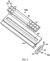
- the optical processing apparatus further includes an illuminance measurement unit 5 for measuring the illuminance of the ultraviolet rays (light) emitted from the LED light source set 400 as shown in Figs. 2 to 4 .
- the illuminance measurement unit 5 includes an illuminance sensor 52 provided to be freely movable by a moving mechanism 51 in the transverse direction on the back side of the case body 40, an optical fiber 53 for transmitting light to the illuminance sensor 52, and a light condensation unit 54 provided at a tip end part of the optical fiber 53.
- the light condensation unit 54 is configured to be capable of moving under the optical irradiation unit 4 from one end to the other end in a lengthwise direction of an irradiation region accompanying the movement of the illuminance sensor 52 in order to condense the light emitted from the LED light source set 400. At times other than measurement in the irradiation region, the light condensation unit 54 stays on standby at a position deviated in the transverse direction from the movement region for a wafer W.
- the light condensation unit 54 has a housing 55 in a square tube-like shape extending in the longitudinal direction. As shown in Fig. 4 , the housing 55 has a slit 56 extending in a lengthwise direction of the light condensation unit 54, that is, in the longitudinal direction. The slit 56 is formed to be longer than the dimension of the strip-shaped irradiation region formed by the LED light source set 400 in regard to a width direction of the irradiation region.
- a light condensation body 57 in a rectangular parallelepiped shape made of fluorescent glass is provided (see Figs. 2 and 3 ).
- the light condensation body 57 emits light at illuminance corresponding to the illuminance of light entering through the slit 56.
- the light condensation body 57 emits light depending on the total illuminance of absorbed light, that is, the total illuminance of four LEDs 41 constituting each light-emitting block 42 (as mentioned earlier, in Fig. 5 , "two" LEDs are shown for convenience). While the height of the top surface of the light condensation body 57 serving as a light-receiving surface coincides with the height of the front surface of the wafer W on the mount 32 in this example, it is not essential to make those heights coincide with each other.
- the total illuminance of the four LEDs 41 constituting each light-emitting block 42 can be measured by leading the light condensed by the light condensation body 57 to the illuminance sensor 52 via the optical fiber 53 and measuring the light intensity with the illuminance sensor 52.
- the illuminance to be acquired by use of the illuminance sensor 52 corresponds to illuminance at each position in the transverse direction in regard to the strip-shaped irradiation region (irradiation region on the wafer W) extending in the transverse direction formed by the set of light-emitting blocks 42.
- An irradiation region formed by each light-emitting block 42 extends not only in the transverse direction but also in the longitudinal direction.
- the aforementioned illuminance at each position in the transverse direction can be evaluated by condensing the light in the irradiation region extending in the longitudinal direction by use of the light condensation unit 54 and measuring illuminance with the illuminance sensor 52.
- the surface illuminance measured with the illuminance sensor 52 is surface illuminance (unit: W/cm 2 )
- the surface illuminance is converted into line illuminance (unit: W/cm) by multiplying the measurement of the surface illuminance with a reference coefficient obtained from the result of preliminary measurement by use of an illuminance sensor.
- the unit of this coefficient is "cm" and the unit length is a length in the transverse direction (lengthwise direction of the aforementioned irradiation region).
- the reason for obtaining the line illuminance is that the line illuminance obtained as the accumulation of light amounts is important in the method in which the wafer W is moved with respect to the strip-shaped irradiation region corresponding to the diameter of the wafer W in the direction orthogonal to the irradiation region (i.e., the irradiation region is scanned relative to the wafer W).
- the position of the illuminance measurement unit 5 illustrated with dotted lines in Fig. 2 indicates the position where the illuminance measurement unit 5 stays on standby when optical processing such as a batch exposure process is performed on the wafer W.
- reference characters B1, B2, ⁇ , and Bn are assigned respectively to the light-emitting blocks from one end to the other end of the arrangement of the light-emitting blocks, for convenience of the explanation.
- the reference character "42" is used for each light-emitting block.
- the reference character 61 represents a drive circuit for driving LEDs 41.
- a plurality of LEDs 41, four LEDs for example are connected in series to each drive circuit 61.
- the drive circuit 61 is provided for each light-emitting block 42.
- the drive circuit 61 includes a phase control circuit, for example, controls the firing angle of a switching element by use of a control signal corresponding to a current command value, thereby controls the conduction angle of the alternating-current waveform, and thereby adjusts the magnitude of the direct current to be equal to the current command value.
- Each drive circuit 61 is included in the control circuit unit 45 shown in Figs. 2 and 3 .
- the control circuit unit 45 includes a bus 62, a CPU 63, and a memory 64 used for work.
- the control circuit unit 45 further includes a first storage unit 65 storing command values of the currents for driving the light-emitting blocks 42 (B1 to Bn), a second storage unit 66 storing an illuminance change amount per unit current which will be explained later, a program storage unit 67 storing programs which will be explained later, and a third storage unit 68 storing a target illuminance distribution pattern. While separate storage units are used for different types of stored data in this example for the sake of convenience, the storage units 65, 66 and 68 in reality are formed as storage areas in the same memory device corresponding to addresses different from each other, for example.
- the controller 60 shown in Fig. 1 having the operation screen, is connected to the bus 62.
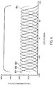
- Fig. 6 is a graph in which the horizontal axis represents the position in the transverse direction in a passage region on the surface of the wafer W and the vertical axis represents the aforementioned line illuminance, where "0" represents a position through which the center of the wafer W passes.
- Each waveform line in the lower part of the graph represents a line illuminance distribution pattern corresponding to each light-emitting block 42 (B1 to Bn), while the line in the upper part of the graph in a shape like a horizontally long flat trapezoid (linear within the diameter of the wafer) represents the illuminance distribution pattern as the sum total of the line illuminances of the light-emitting blocks 42 (B1 to Bn).
- Fig. 6 is a graph in which the horizontal axis represents the position in the transverse direction in a passage region on the surface of the wafer W and the vertical axis represents the aforementioned line illuminance, where "0" represents a position through which the center of
- the illuminance distribution pattern on the wafer W surface corresponding to each light-emitting block 42 (B1 to Bn) can be adjusted by adjusting the light intensity of each light-emitting block 42 (B1 to Bn), that is, by adjusting the value of the current (drive current) of each light-emitting block 42 (B1 to Bn).
- the illuminance distribution pattern as the sum total of the line illuminances of the light-emitting blocks 42 (B1 to Bn) can be adjusted by adjusting the current value of each light-emitting block 42 (B1 to Bn).
- the LED characteristics slightly vary among individual LEDs due to manufacturing errors or the like, and thus the illuminance distribution pattern of each LED is not necessarily equal to each other even if the same current is fed to each LED. Further, even if the value of the current fed to an LED remains constant, the light-emitting intensity gradually drops due to variation of the LED with time. Therefore, it is desirable to design the overall structure, including the selection of the LEDs, so that a necessary illuminance distribution is obtained when a current lower than the LED's maximum allowable current value, such as a current at 70% of the maximum allowable current value, is fed to each LED at the start of use. With such design, even if the light-emitting intensity of each LED gradually drops, a necessary light-emitting intensity can be secured by increasing the current value, and the service life of the LEDs can be extended.
- the second storage unit 66 stores an illuminance change amount at each position in a case where the current value of the current (drive current) fed to each light-emitting block 42 is gradually increased within a range of 70% to 100% of the maximum allowable current value, for example.
- the illuminance change amount means the amount of change in the illuminance at each position with respect to a change in the current when the current is changed (which can be referred to also as a change amount of the illuminance per unit current value).
- the "position” means the position on the wafer W in the transverse direction.
- the data associating each position and the illuminance change amount can be represented as an illuminance profile (illuminance distribution pattern) as schematically shown beside the second storage unit 66 in Fig. 5 .
- the second storage unit 66 stores an illuminance distribution response amount of each light-emitting block B1 to Bn as P1 to Pn.
- the illuminance distribution pattern as the illuminance profile indicates how much the illuminance at each position changes per unit current, e.g., per 0.1 mA when the unit current is determined as 0.1 mA, which can be regarded as the "response" of the illuminance distribution pattern to the change in the current, or the "gradient" of the illuminance distribution pattern with respect to the current value.
- the term "illuminance distribution response amount” will be used to mean the “response (gradient).” Since the illuminance change amount corresponds to the amount of change in the aforementioned line illuminance, the unit of the illuminance change amount is in the dimension (W/cm ⁇ A) obtained by dividing energy (W) by unit length (cm) and unit current value (A). However, in regard to the data of the illuminance distribution response amount written to the second storage unit 66, the unit of the illuminance change amount may also be defined as "W/cm” by regarding the illuminance change amount as the value of the illuminance change amount (illuminance change) itself when the current is changed by 0.1 mA, for example. Namely, the vertical axis of the graph shown beside the second storage unit 66 in Fig. 5 may also be in the dimension (W/cm) obtained by multiplying the illuminance change amount (W/cm ⁇ A) by the current value (A).
- each light-emitting block 42 (B1 to Bn) Once the illuminance distribution response amount of each light-emitting block 42 (B1 to Bn) is acquired, it becomes clear how much change in the presently obtained illuminance distribution pattern of each light-emitting block 42 (B1 to Bn) (i.e., the illuminance distribution pattern in regard to each light-emitting block B1 to Bn) is caused by how much change in the presently used drive current. Since the illuminance distribution pattern formed in the whole wafer W passage region by the LED light source set 400 is represented by the sum total of the individual illuminance distribution patterns of the light-emitting blocks B1 to Bn, how much the total illuminance distribution pattern changes in the end can be grasped.
- the mechanism described above is used for the light amount adjustment at the start of use of the optical processing apparatus and the regular or irregular calibration.
- the drive current is set at 70% of the maximum allowable current value, for example, the drive current is increased in units of 0.1 mA, for example, and the illuminance distribution pattern is obtained by measuring the illuminance at each position with the illuminance sensor 52 at each current value. This operation is performed successively for all the light-emitting blocks B1 to Bn.
- the drive current is increased in units of 0.1 mA, for example, the illuminance change amount is supposed to remain constant at every value of the drive current.
- the illuminance change amounts each obtained at each change in the current value are averaged and the average is stored in the second storage unit 66 as the illuminance change amount of the light-emitting block 42.
- the decrease (decrement) corresponds to the increase (increment) in the case of increasing the drive current, and thus the illuminance distribution response amount of each light-emitting block B1 to Bn can be acquired in a similar manner.
- the work time can be shortened since it is unnecessary to turn off the LEDs 41.
- the program storage unit 67 stores a data acquisition program 67a for acquiring the aforementioned illuminance distribution response amount, an illuminance adjustment program 67b for adjusting the light amount (light intensity) of each light-emitting block B1 to Bn at the start of use of the apparatus, a calibration program 67c for performing calibration regularly or irregularly, and so forth.
- the data acquisition program 67a is a program for acquiring the illuminance distribution response amount by performing steps like the increasing/decreasing of the drive current, movement control of the illuminance sensor 52, writing of the data of the illuminance change amount at each position, and so forth when the illuminance change amount of each light-emitting block B1 to Bn is obtained.
- the illuminance adjustment program 67b and the calibration program 67c include steps for bringing the present illuminance distribution pattern in the lengthwise direction in the irradiation region close to a target illuminance distribution pattern as will be explained later.
- the steps are for determining a new current command value based on the change amount of the illuminance distribution pattern and the present current command value of each of the light-emitting blocks B1 to Bn. These steps correspond to an arithmetic processing unit as a component in the present invention.
- the program storage unit 67 also stores a program for controlling a series of operations of the mount 32, etc. from the loading of the wafer W into the housing 30 to the unloading of the wafer W from the housing 30.
- the above-described programs are stored in a non-transitory computer-readable storage medium such as a flexible disk, a compact disc, a hard disk, a magneto-optical (MO) disk or a memory card, and are installed in the program storage unit 67 from the storage medium via the controller 60.
- a non-transitory computer-readable storage medium such as a flexible disk, a compact disc, a hard disk, a magneto-optical (MO) disk or a memory card
- each light-emitting block B1 to Bn is turned on (i.e., driven into the light-emitting state) and after the time for the stabilization of light emission has elapsed, the illuminance distribution response amount of each light-emitting block B1 to Bn is acquired according to the data acquisition program 67a (step S1).
- the operation for the acquisition of the illuminance distribution response amount has already been explained in detail, and thus repeated explanation thereof is omitted here. Subsequently, as shown in Fig.
- step S2 data of the target illuminance distribution pattern in regard to the illuminance distribution pattern in the lengthwise direction in the (whole) irradiation region is inputted to the third storage unit 68 of the control circuit unit 45 from the controller 60 shown in Figs. 1 and 5 (step S2).
- the drive current of each light-emitting block B1 to Bn is provisionally set at a current value lower than the maximum allowable current value, such as 70% of the maximum allowable current value (step S3).
- the current value is written to the first storage unit 65 as the current command value of each light-emitting block B1 to Bn.
- the illuminance at each position is measured by moving the illuminance measurement unit 5 from one end to the other end of the irradiation region, and the total illuminance distribution pattern in the lengthwise direction of the irradiation region is obtained by converting the measured illuminances into the line illuminance as explained above (step S4).
- step S5 difference is obtained between the target illuminance distribution pattern inputted in the step S2 and the illuminance distribution pattern obtained in the step S4, and the current command value of each light-emitting block B1 to Bn is adjusted so as to make the difference approach zero, that is, so as to make the illuminance difference at each position approach zero (step S5).
- the illuminance distribution pattern of each light-emitting block B1 to Bn is determined according to the increase/decrease (increment/decrement) and the illuminance distribution response amount of each light-emitting block B1 to Bn, and the illuminance distribution pattern in the whole irradiation region can be obtained by calculating the sum of these illuminance distribution patterns.
- the work of adjusting the current command value is a process of searching for an increment/decrement that makes the aforementioned difference zero by varying the current value increment/decrement of each light-emitting block B1 to Bn in various ways. The process is performed by the illuminance adjustment program 67b corresponding to the arithmetic processing unit.
- FIG. 8 schematic diagrams for intuitively grasping how the illuminance distribution pattern is adjusted by using the current command values are shown in Fig. 8 .
- the reference characters Ak, A(k+1) and A(k+2) respectively represent illuminance distribution patterns in the irradiation region formed on the wafer W by three light-emitting blocks Bk, B(k+1) and B(k+2) aligned consecutively. Illuminance distribution patterns formed by light-emitting blocks on both sides of the line of light-emitting blocks Bk, B(k+1) and B(k+2) are omitted in Fig. 8 .
- the reference character 500 represents the target illuminance distribution pattern
- the reference character 600 represents the illuminance distribution pattern formed by the respective light-emitting blocks. Since the illuminance distribution pattern A(k+1) is especially low, a part of the total illuminance distribution pattern corresponding to the light-emitting block B(k+1) has become especially low.
- each illuminance distribution pattern Ak, A(k+1), A(k+2) is raised/lowered by increasing/decreasing the present current command value of each light-emitting block Bk, B(k+1), B(k+2) by using the illuminance distribution response amounts Pk, P(k+1), P(k+2) of the respective light-emitting block Bk, B(k+1), B(k+2).
- the respective illuminance distribution patterns Ak, A(k+1), A(k+2) are raised, as indicated by dotted lines, by increasing the current command values of the respective light-emitting block Bk, B(k+1), B(k+2). Accordingly, the total illuminance distribution pattern 600 is pushed up to an illuminance distribution pattern approximate to the target illuminance distribution pattern 500.
- This current command value adjustment work is performed by using the least-squares method, for example, by squaring the difference between the illuminance at each position in the target illuminance distribution pattern and the illuminance at each position in the present illuminance distribution pattern and determining a combination of current command values of the light-emitting blocks B1 to Bn minimizing the sum total of the squared values at the positions.
- each current command value is stored in the first storage unit 65 (step S6).
- the current command values are described as I1 to In.
- the current command values read out from the first storage unit 65 are sent to the drive circuits 61 and the light-emitting blocks B1 to Bn are driven by currents corresponding to the current command values.
- the wafer W constituting a substrate as the workpiece is handed over by an external transfer arm to the mount 32 situated at the handover position in the housing 30 via the carry-in/carry-out port 31 shown in Fig. 1 . Then, the mount 32 is moved to the standby position in a state with the shutter 46 of the optical irradiation unit 4 closed, for example, and the positioning of the wafer W is carried out. As a result of the positioning, an alignment direction of a circuit chip region on the wafer W coincides with the lengthwise direction of the irradiation region, for example.
- the shutter 46 of the optical irradiation unit 4 is opened and the mount 32 is moved from the standby position towards the handover position (forward). Accordingly, the wafer W gradually passes through the strip-shaped irradiation region under the optical irradiation unit 4. In other words, the strip-shaped irradiation region relatively scans the surface of the wafer W.
- the illuminance distribution pattern has been adjusted to the target illuminance distribution pattern such as an illuminance distribution pattern uniform in the lengthwise direction with high accuracy, and thus the amount of exposure becomes uniform throughout the wafer W.
- the wafer W that returned to the handover position is taken out by the external transfer arm.
- the calibration of the LED light source set 400 is performed regularly, for example. This is because the amount of light emission of each LED gradually drops along with use as mentioned earlier and the drive current has to be increased. While the calibration is performed similarly to the light amount adjustment work performed at the start of the operation of the apparatus, the target illuminance distribution pattern and the illuminance distribution response amount of each light-emitting block 42 have already been inputted and the current command values have already been set, and thus only the steps S4 to S6 in the flow shown in Fig. 7 are carried out.
- the illuminance distribution pattern is obtained by measuring the present illuminance with the illuminance sensor 52 in the lengthwise direction of the irradiation region, current values that make the illuminance distribution pattern as close to the target illuminance distribution pattern as possible are obtained, and the obtained current values are specified as the new current command values.
- the illuminance distribution response amount as the change amount of the illuminance distribution pattern (illuminance profile), associating the position in the irradiation region in the lengthwise direction with the change amount of the illuminance with respect to the change in the current (drive current), has previously been acquired for each light-emitting block 42. Then, by using the illuminance distribution response amount, the illuminance distribution pattern of each light-emitting block 42 is obtained, and the illuminance distribution pattern of all the light-emitting blocks in the lengthwise direction is estimated by obtaining the sum of the illuminance distribution patterns of the light-emitting blocks 42.
- the illuminance distribution pattern in the lengthwise direction of the irradiation region can be adjusted to the target illuminance distribution pattern with ease and with high accuracy, and difference in the illuminance distribution pattern among a plurality of optical processing apparatuses can be kept down.
- the optical processing apparatus described above may also be configured to include an LED monitoring unit for monitoring the operating status of each light-emitting block 42 and to detect an abnormal light-emitting block including a light-emitting diode that abnormally dropped in the amount of light emission or stopped light emission.
- the LED monitoring unit may be, for example, a circuit that monitors the current of each light-emitting block 42 and outputs an abnormality detection signal when the current drops to or below a threshold value, or may employ the illuminance sensor 52. In cases where the illuminance sensor 52 is employed, the illuminance sensor 52 is moved and the illuminance is measured upon each processing of a wafer W or at times like before starting the processing of each lot (a set of wafers in units of carriers C).
- An abnormal light-emitting block 42 can be detected by judging whether or not the illuminance at the position corresponding to each light-emitting block 42, e.g., at the position corresponding to the center of the LEDs of each light-emitting block 42, has dropped to or below a threshold value based on the result of the measurement.
- the abnormality detection signal is outputted, the calibration program 67c corresponding to an execution processing unit is activated according to the output, for example, and the flow from the step S4 in Fig. 7 is carried out.
- the illuminance sensor 52 is employed as the LED monitoring unit, the present illuminance distribution pattern may be obtained in the illuminance measurement for detecting an abnormal light-emitting block.
- the optical processing can be continued even when an abnormality has occurred to a light-emitting block 42. Accordingly, there are advantages in that the occurrence of a downtime of the apparatus can be avoided and the service life of the apparatus can be extended.
- the target illuminance distribution pattern in the above-described embodiment is assumed to be uniform in the movement region of the wafer W, for example, the target illuminance distribution pattern may be set flexibly depending on the role the apparatus is required to play. For example, when the line width of the pattern on one surface of the wafer W tends to be narrow at the stage of preprocessing, it is possible to make a setting like lowering the illuminance of the irradiation region corresponding to the one surface in comparison with the other surface.
- the illuminance measurement unit 5 is configured to be freely movable in the transverse direction to have the illuminance sensor 52 scan the illuminance at each position in the above-described example, the illuminance measurement unit 5 may also be configured in the fixed type to measure the illuminance in the irradiation region all at once.
- the workpiece processed by the optical processing apparatus is not limited to a wafer W coated with a resist of the photosensitization chemical amplification type; the optical processing apparatus can be an apparatus that performs sensitization and/or line width adjustment on a wafer W coated with an ordinary type of resist.
- the optical processing apparatus may also be, for example, an apparatus that irradiates a carbon film, as a coating film to serve as a protective film at the time of dry etching, with light to promote a crosslinking reaction in the carbon film and thereby increase the carbon film's resistance to the etching, or an apparatus that promotes the curing of a resist film.
- the optical processing apparatus may also be an apparatus for curing an organic film, or an apparatus for adjusting the film thickness of a lower layer film in a coating film by irradiating the wafer W with light.
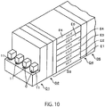
- the coating/development apparatus 1 is formed by connecting a carrier block D1, an inspection block D2, a processing block D3 and an interface block D4 linearly in a lateral direction.
- An exposure device D5 is connected to the interface block D4.
- the carrier block D1 includes mount stages 11 on each of which a carrier C storing a wafer W being a circular substrate can be placed.
- the reference character 12 represents an open/close part and the reference character 13 represents a transfer mechanism for transferring the wafer W between the carrier C and the inspection block D2.
- the inspection block D2 is provided with two inspection devices 23 arranged side by side as viewed from the carrier block D1 side.
- a handover stage 10 on which the wafer W is temporarily set is provided on the carrier block D1 side of a space between the inspection devices 23, while a transfer mechanism 19 for handing over the wafer W among the handover stage 10, the inspection devices 23 and the processing block D3 is provided on the processing block D3 side of the space between the inspection devices 23.
- the inspection devices 23 perform inspection of the line width of the pattern formed on the wafer W after the development process.
- the wafer W is divided in its radial direction into subregions, the line width of the pattern in each subregion is detected, and the position of each subregion on the wafer W and the line width of the pattern are associated with each other and stored in a control unit 100 as pattern information.
- the processing block D3 is formed by stacking up unit blocks E1 to E6, each for performing liquid treatment on the wafer W, in this order from the bottom.
- the transfer and processing of wafers W are carried out in parallel with each other.
- the unit blocks E1 and E2 are configured in the same way as each other, the unit blocks E3 and E4 are configured in the same way as each other, and the unit blocks E5 and E6 are configured in the same way as each other.
- a transfer region F5 extending from the inspection block D2 to the interface block D4, a plurality of rack units U are arranged in the longitudinal direction.
- two development modules 21 are arranged in the longitudinal direction.
- the development module 21 supplies a developing solution to a resist film formed on the surface of the wafer W.
- Each rack unit U includes a heating module 22 for heating the wafer W and a batch exposure device 3 as the optical processing apparatus.
- the aforementioned transfer region F5 is provided with a transfer arm 14 as a wafer W transfer mechanism.
- the wafer W is transferred among modules arranged in the unit block E5 and modules in towers T1 and T2 explained later arranged at the same height as the unit block E5.
- the unit blocks E1 to E4 are configured in the same way as the unit blocks E5 and E6 except for the fact that the chemical solutions supplied to the wafer W are different.
- Each of the unit blocks E1 and E2 includes antireflective film formation modules for supplying a chemical solution for forming an antireflective film to the wafer W instead of the development modules 21.
- Each of the unit blocks E3 and E4 includes resist film formation modules for supplying a resist of the chemical amplification type to the wafer W as the chemical solution and thereby forming a resist film instead of the development modules 21.
- a tower T1 extending vertically across the unit blocks E1 to E6 and a handover arm 15 as an elevatable handover mechanism for handing over the wafer W to the tower T1 are arranged on the inspection block D2 side of the processing block D3.
- the tower T1 is formed of a plurality of modules stacked up, and includes handover modules on each of which a wafer W can be set.
- the interface block D4 includes towers T2, T3 and T4 extending vertically across the unit blocks E1 to E6.
- the interface block D4 is provided with an interface arm 16 as an elevatable handover mechanism for handing over a wafer W to the towers T2 and T3, an interface arm 17 as an elevatable handover mechanism for handing over a wafer W to the towers T2 and T4, and an interface arm 18 for handing over a wafer W between the tower T2 and the exposure device D5.
- the exposure device D5 exposes the surface of the wafer W by using a pattern mask.
- the tower T2 is formed by stacking up handover modules, a buffer module for storing and retaining a plurality of wafers W before the exposure process, a buffer module for storing a plurality of wafers W after the exposure process, a temperature control module for performing temperature control of the wafers W, and so forth.
- the reference character 100 represents the control unit. The control unit 100 performs transfer control of the wafers W in the coating/development apparatus 1 and management of process recipes.
- the processing of the wafer W in the system formed of the coating/development apparatus 1 and the exposure device D5 described above will be explained below.
- the wafer W is transferred by the transfer mechanism 13 from a carrier C and is placed on the handover stage 10 in the inspection block D2.
- the wafer W is transferred by the transfer mechanism 19 to a handover module of the tower T1 in the processing block D3.
- the wafer W is distributed by the handover arm 15 to one of the handover modules of the tower T1 each corresponding to the unit blocks E1 and E2 and thereafter transferred.
- the wafer W after being distributed as above is transferred in the order of the handover module, the antireflective film formation module, the heating module, and the handover module, and subsequently distributed by the handover arm 15 to one of the handover modules each corresponding to the unit blocks E3 and E4.
- the wafer W distributed to the handover module in this way is transferred to a corresponding resist film formation module, in which a resist film is formed by coating the whole surface of the wafer W with a resist of the photosensitization chemical amplification type.
- the wafer W is transferred in the order of the heating module and the handover module of the tower T2, and thereafter loaded into the exposure device D5 via the tower T3.
- the exposure process is performed by use of a pattern mask. Accordingly, acid and photosensitizer are generated in regions on the wafer W pattern-exposed by the exposure process.
- the wafer W after undergoing the pattern exposure is transferred to the unit block E5 or E6. Thereafter, in the batch exposure device 3 as the optical processing apparatus, the whole surface of the wafer W undergoes exposure, the aforementioned photosensitizer absorbs light, and acid and photosensitizer are generated further in the pattern-exposed regions. Due to the batch exposure performed as above, acid multiplies in the pattern-exposed regions in the resist film. Thereafter, the wafer W is transferred to the heating module 22 and heated. In the heating module 22, the pattern-exposed regions are modified due to the acid and becomes soluble to the developing solution.
- the wafer W is transferred to the development module 21, in which the developing solution is supplied to the wafer W, the modified regions are dissolved in the developing solution, and the resist pattern in formed. Thereafter, the wafer W is transferred to the tower T1, then loaded into the carrier block D1 through the inspection block D2, and returned to the carrier C via the transfer mechanism 13.
- film deposition is carried out by using an inspection wafer prior to the processing of the wafer W as the product, for example, and the illuminance of each cell of the LED light source set 400 in the batch exposure device 3 is determined based on pattern information on the inspection wafer obtained by the inspection device 23.
Landscapes
- Physics & Mathematics (AREA)
- General Physics & Mathematics (AREA)
- Exposure And Positioning Against Photoresist Photosensitive Materials (AREA)
- Exposure Of Semiconductors, Excluding Electron Or Ion Beam Exposure (AREA)
- Photosensitive Polymer And Photoresist Processing (AREA)
- Length Measuring Devices By Optical Means (AREA)
Claims (12)
- Optische Verarbeitungsvorrichtung, umfassend:ein Montageteil (32), auf das ein Werkstück (W) gesetzt wird, das mit Licht verarbeitet werden soll;eine optische Bestrahlungseinheit (4), in der eine Vielzahl von lichtemittierenden Blöcken (42), die jeweils aus einer Leuchtdiode (41) oder einer Vielzahl in Reihe geschalteter Leuchtdioden (41) bestehen, linear in Querrichtung zum Bilden eines streifenförmigen Bestrahlungsbereichs angeordnet sind, der sich in der Querrichtung erstreckt; undeinen Bewegungsmechanismus (51) zum Bewegen des Montageteils (32) und der optischen Bestrahlungseinheit (4) relativ zueinander in einer Längsrichtung;dadurch gekennzeichnet, dass die Vorrichtung weiter umfasst:eine Speichereinheit (66), die ausgelegt ist, um einen Änderungsbetrag eines Beleuchtungsstärken-Verteilungsmusters zu speichern, wobei jede Position in dem Bestrahlungsbereich in der Querrichtung einem Änderungsbetrag der Beleuchtungsstärke an jeder Position in Bezug auf eine Stromänderung im Hinblick auf jeden der lichtemittierenden Blöcke (42) zugeordnet ist; undeine arithmetische Verarbeitungseinheit, die ausgelegt ist, um einen Strombefehlswert von jedem der lichtemittierenden Blöcke (42) basierend auf einem Strombefehlswert von jedem der lichtemittierenden Blöcke (42) und dem Änderungsbetrag des Beleuchtungsstärken-Verteilungsmusters jedes der lichtemittierenden Blöcke (42) zu bestimmen, die in der Speichereinheit (66) gespeichert sind, um ein vorhandenes Beleuchtungsstärken-Verteilungsmuster in dem Bestrahlungsbereich in einer Längsrichtung nahe an ein Ziel-Beleuchtungsstärken-Verteilungsmuster zu bringen.
- Optische Verarbeitungsvorrichtung nach Anspruch 1, wobei der Änderungsbetrag der Beleuchtungsstärke in Bezug auf die Stromänderung ein Änderungsbetrag der Linienbeleuchtungsstärke in der Querrichtung ist, der basierend auf der Oberflächenbeleuchtungsstärke an jeder Position erhalten wird.
- Optische Verarbeitungsvorrichtung nach Anspruch 1 oder 2,
umfassend eine Beleuchtungsstärken-Messeinheit (5) zum Messen der Beleuchtungsstärke in dem Bestrahlungsbereich. - Optische Verarbeitungsvorrichtung nach Anspruch 3, wobei die Beleuchtungsstärken-Messeinheit (5) konfiguriert ist, um in einer Ausrichtungsrichtung der lichtemittierenden Blöcke (42) bewegbar zu sein.
- Optische Verarbeitungsvorrichtung nach Anspruch 3 oder 4, wobei die Beleuchtungsstärken-Messeinheit (5) beinhaltet:ein streifenförmiges Lichtaufnahmeloch (56), das sich in der Längsrichtung erstreckt;ein prismatisches Teil (57), das derart angeordnet ist, dass streifenförmiges Licht, das durch das Lichtaufnahmeloch (56) aufgenommen wird, auf eine andere Oberfläche als zwei Endflächen einfällt, und das Licht aus einer der zwei Endflächen austritt; undeinen Beleuchtungsstärkensensor (52), der das Licht aufnimmt, das von der Endfläche des prismatischen Teils (57) austritt.
- Optische Verarbeitungsvorrichtung nach einem der Ansprüche 1 bis 5, umfassend:eine LED-Überwachungseinheit (52), die den Betriebszustand der lichtemittierenden Blöcke (42) überwacht; undeine Ausführungsverarbeitungseinheit (67c), die einen Schritt des Erhaltens des Beleuchtungsstärken-Verteilungsmusters in Längsrichtung durch Erfassen der Beleuchtungsstärke in dem Bestrahlungsbereich ausführt, der durch die optische Bestrahlungseinheit (4) mit einer Beleuchtungsstärken-Messeinheit (5) gebildet wird, wenn ein anormaler lichtemittierender Block (42), der eine Leuchtdiode (41) beinhaltet, die in dem Lichtemissionsbetrag anormal abgefallen ist oder die Lichtemission angehalten hat, durch die LED-Überwachungseinheit (52) erfasst wird, und einen Schritt des Bestimmens des Strombefehlswerts jedes der lichtemittierenden Blöcke (42) mit der arithmetischen Verarbeitungseinheit basierend auf dem derzeitigen Stromwert jedes der lichtemittierenden Blöcke (42) und dem Änderungsbetrag des Beleuchtungsstärken-Verteilungsmusters jedes der lichtemittierenden Blöcke (42), die in der Speichereinheit (66) gespeichert sind, um das Beleuchtungsstärken-Verteilungsmuster, das durch den vorherigen Schritt erhalten wurde, nahe des Ziel-Beleuchtungsstärken-Verteilungsmusters zu bringen.
- Optische Verarbeitungsvorrichtung nach einem der Ansprüche 1 bis 6, wobei die optische Verarbeitungsvorrichtung eine Vorrichtung ist, die eine Musterbelichtung auf einem Substrat (W), auf dem ein Resistfilm gebildet ist, unter Verwendung einer Mustermaske durchführt und danach die Belichtung auf einem musterbelichteten Bereich durchführt.
- Beschichtungs-/Entwicklungsvorrichtung (1), umfassend:ein Modul (E3, E4) zum Bilden eines Resistfilms auf einem Substrat (W) unter Verwendung einer Beschichtungsflüssigkeit;ein Modul (21) zum Entwickeln des Substrats (W) nach der Musterbelichtung;einen Übertragungsmechanismus (14) zum Übertragen des Substrats (W) zwischen den Modulen; unddie optische Verarbeitungsvorrichtung nach einem der Ansprüche 1 bis 7.
- Optisches Verarbeitungsverfahren zum Verarbeiten eines Werkstücks (W) mit Licht, wobei:
das optische Verarbeitungsverfahren verwendet:eine optische Bestrahlungseinheit (4), in der eine Vielzahl von lichtemittierenden Blöcken (42), die jeweils aus einer Leuchtdiode (41) oder einer Vielzahl in Reihe geschalteter Leuchtdioden (41) bestehen, linear in Querrichtung zum Bilden eines streifenförmigen Bestrahlungsbereichs angeordnet sind, der sich in der Querrichtung erstreckt; undeine Speichereinheit (66), die einen Änderungsbetrag eines Beleuchtungsstärken-Verteilungsmusters speichert, wobei jede Position in dem Bestrahlungsbereich in der Querrichtung einem Änderungsbetrag der Beleuchtungsstärke an jeder Position in Bezug auf eine Stromänderung im Hinblick auf jeden der lichtemittierenden Blöcke (42) zugeordnet ist, unddas optische Verarbeitungsverfahren die folgenden Schritte umfasst:Bestimmen eines Strombefehlswerts von jedem der lichtemittierenden Blöcke (42) basierend auf einem derzeitigen Strombefehlswert von jedem der lichtemittierenden Blöcke (42) und dem Änderungsbetrag des Beleuchtungsstärken-Verteilungsmusters jedes der lichtemittierenden Blöcke (42), die in der Speichereinheit (66) gespeichert sind, um ein vorhandenes Beleuchtungsstärken-Verteilungsmuster in dem Bestrahlungsbereich in der Längsrichtung nahe an ein Ziel-Beleuchtungsstärken-Verteilungsmuster zu bringen;Veranlassen, dass jeder der lichtemittierenden Blöcke (42) Licht mit dem Strombefehlswert emittiert, der durch den vorherigen Schritt bestimmt wurde; undanschließendes Bewegen der optischen Bestrahlungseinheit (4) und eines Montageteils (32), auf dem das Werkstück (W) aufgesetzt ist, relativ zueinander in einer Längsrichtung. - Optisches Verarbeitungsverfahren nach Anspruch 9, wobei ein Schritt des Messens der Beleuchtungsstärke in dem Bestrahlungsbereich vor dem Schritt des Bestimmens des Strombefehlswerts durchgeführt wird.
- Optisches Verarbeitungsverfahren nach Anspruch 9 oder 10, umfassend die folgenden Schritte:Überwachen des Betriebszustands der lichtemittierenden Blöcke (42);Erhalten des Beleuchtungsstärken-Verteilungsmusters in der Längsrichtung durch Erfassen der Beleuchtungsstärke in dem Bestrahlungsbereich, der durch die optische Bestrahlungseinheit (4) gebildet wird, wenn ein anormaler lichtemittierender Block (42), der eine Leuchtdiode (41) aufweist, die in dem Lichtemissionsbetrag anormal abgefallen ist oder die Lichtemission angehalten hat, durch den vorherigen Schritt erkannt wird; undBestimmen des Strombefehlswerts von jedem der lichtemittierenden Blöcke (42) basierend auf dem derzeitigen Strombefehlswert von jedem der lichtemittierenden Blöcke (42) und dem Änderungsbetrag des Beleuchtungsstärken-Verteilungsmusters jedes der lichtemittierenden Blöcke (42), die in der Speichereinheit (66) gespeichert sind, um das Beleuchtungsstärken-Verteilungsmuster, das durch den vorherigen Schritt erhalten wurde, nahe des Ziel-Beleuchtungsstärken-Verteilungsmuster zu bringen.
- Nichtflüchtiges computerlesbares Speichermedium, das ein Computerprogramm speichert, das für eine Vorrichtung verwendet wird, die eine Verarbeitung eines Werkstücks (W) durch Bestrahlen des Werkstücks (W) mit Licht durchführt, und beinhaltet:eine optische Bestrahlungseinheit (4), in der eine Vielzahl von lichtemittierenden Blöcken (42), die jeweils aus einer Leuchtdiode (41) oder einer Vielzahl von in Reihe geschalteten Leuchtdioden (41) gebildet sind, in einer Querrichtung linear angeordnet ist, um einen streifenförmigen Bestrahlungsbereich zu bilden; undeine Speichereinheit (66), die einen Änderungsbetrag eines Beleuchtungsstärken-Verteilungsmusters speichert, wobei jede Position in dem Bestrahlungsbereich in der Querrichtung einem Änderungsbetrag der Beleuchtungsstärke an der Position bezüglich jedes der lichtemittierenden Blöcke (42) pro Einheit Strom zugeordnet ist,wobei das Computerprogramm Schritte beschreibt, die programmiert sind, um das optische Verarbeitungsverfahren nach einem der Ansprüche 9 bis 11 auszuführen.
Applications Claiming Priority (1)
| Application Number | Priority Date | Filing Date | Title |
|---|---|---|---|
| JP2016246677A JP6866631B2 (ja) | 2016-12-20 | 2016-12-20 | 光処理装置、塗布、現像装置、光処理方法及び記憶媒体 |
Publications (2)
| Publication Number | Publication Date |
|---|---|
| EP3346337A1 EP3346337A1 (de) | 2018-07-11 |
| EP3346337B1 true EP3346337B1 (de) | 2019-09-04 |
Family
ID=60811780
Family Applications (1)
| Application Number | Title | Priority Date | Filing Date |
|---|---|---|---|
| EP17207286.0A Active EP3346337B1 (de) | 2016-12-20 | 2017-12-14 | Optische verarbeitungsvorrichtung, beschichtungs-/entwicklungsvorrichtung, optisches verarbeitungsverfahren und nicht transitorisches computerlesbares speichermedium |
Country Status (6)
| Country | Link |
|---|---|
| US (1) | US10527948B2 (de) |
| EP (1) | EP3346337B1 (de) |
| JP (1) | JP6866631B2 (de) |
| KR (1) | KR102482213B1 (de) |
| CN (1) | CN108205242B (de) |
| TW (1) | TWI746736B (de) |
Families Citing this family (11)
| Publication number | Priority date | Publication date | Assignee | Title |
|---|---|---|---|---|
| JP2021015240A (ja) * | 2019-07-16 | 2021-02-12 | 株式会社Screenホールディングス | 光源装置の補正方法、光源装置および描画装置 |
| NL2023537B1 (en) * | 2019-07-19 | 2021-02-08 | Xeikon Prepress Nv | Apparatus and method for exposure of relief precursors |
| WO2021048746A1 (zh) * | 2019-09-10 | 2021-03-18 | 默司科技股份有限公司 | 智慧光罩及其曝光设备、曝光方法和曝光图案形成方法 |
| KR102184871B1 (ko) * | 2019-12-11 | 2020-12-01 | 주식회사 씨티랩 | 웨이퍼 세정 장치용 조명 장치 및 이를 이용한 세정 장치 |
| CN115668046B (zh) * | 2020-05-21 | 2026-02-24 | 凤凰电机公司 | 光照射装置及具备其的曝光装置 |
| JP7566421B2 (ja) * | 2020-11-13 | 2024-10-15 | 株式会社ディスコ | 紫外線照射装置及び紫外線照射装置の管理方法 |
| KR102650608B1 (ko) * | 2020-12-18 | 2024-03-25 | 세메스 주식회사 | 광 처리 부재, 그를 포함하는 기판 처리 장치 및 기판 처리 방법 |
| CN113566955B (zh) * | 2021-09-27 | 2022-03-01 | 深圳易来智能有限公司 | 桌面照度获取方法和照明设备、存储介质及电子装置 |
| CN114911141B (zh) * | 2022-07-11 | 2022-09-23 | 上海传芯半导体有限公司 | Euv光刻方法及euv光刻设备 |
| JPWO2024135474A1 (de) * | 2022-12-20 | 2024-06-27 | ||
| CN120559962A (zh) * | 2025-07-01 | 2025-08-29 | 浙江载力科技有限公司 | 一种uv-led移动扫描式光刻方法及装置 |
Family Cites Families (18)
| Publication number | Priority date | Publication date | Assignee | Title |
|---|---|---|---|---|
| JPH1092722A (ja) * | 1996-09-18 | 1998-04-10 | Nikon Corp | 露光装置 |
| JPH11274069A (ja) * | 1998-03-19 | 1999-10-08 | Nikon Corp | 露光方法および装置 |
| JP2003215809A (ja) * | 2002-01-28 | 2003-07-30 | Pentax Corp | 露光装置および露光方法 |
| JP2005070069A (ja) * | 2003-08-21 | 2005-03-17 | Canon Inc | 画像形成装置 |
| JP4279738B2 (ja) * | 2004-07-22 | 2009-06-17 | リンテック株式会社 | 紫外線照射装置 |
| JP4942301B2 (ja) * | 2004-11-30 | 2012-05-30 | 新光電気工業株式会社 | 直接露光装置および直接露光方法 |
| JP5117709B2 (ja) * | 2006-12-04 | 2013-01-16 | リンテック株式会社 | 紫外線照射装置及び紫外線照射方法 |
| JP4762940B2 (ja) * | 2007-03-13 | 2011-08-31 | 株式会社小糸製作所 | 車両用灯具 |
| US8699001B2 (en) * | 2009-08-20 | 2014-04-15 | Nikon Corporation | Object moving apparatus, object processing apparatus, exposure apparatus, object inspecting apparatus and device manufacturing method |
| JP5165731B2 (ja) * | 2010-06-30 | 2013-03-21 | 東京エレクトロン株式会社 | 局所露光装置及び局所露光方法 |
| JP5541198B2 (ja) * | 2011-03-01 | 2014-07-09 | ウシオ電機株式会社 | 光照射装置 |
| JP5325907B2 (ja) * | 2011-02-22 | 2013-10-23 | 東京エレクトロン株式会社 | 局所露光装置 |
| JP2013104934A (ja) * | 2011-11-11 | 2013-05-30 | Tokyo Electron Ltd | 露光装置及び露光方法 |
| JP5836848B2 (ja) * | 2012-03-06 | 2015-12-24 | 東京エレクトロン株式会社 | 補助露光装置 |
| KR101532352B1 (ko) * | 2013-10-30 | 2015-06-29 | 주식회사 인피테크 | 노광용 led 광원 장치 및 노광용 led 광원장치 관리시스템 |
| JP6337757B2 (ja) | 2014-01-20 | 2018-06-06 | 東京エレクトロン株式会社 | 露光装置、レジストパターン形成方法及び記憶媒体 |
| JP6403445B2 (ja) * | 2014-06-09 | 2018-10-10 | 株式会社キーエンス | 検査装置、検査方法およびプログラム |
| NL2014572B1 (en) * | 2015-04-01 | 2017-01-06 | Suss Microtec Lithography Gmbh | Method for regulating a light source of a photolithography exposure system and exposure assembly for a photolithography device. |
-
2016
- 2016-12-20 JP JP2016246677A patent/JP6866631B2/ja active Active
-
2017
- 2017-12-01 US US15/828,870 patent/US10527948B2/en active Active
- 2017-12-13 KR KR1020170171385A patent/KR102482213B1/ko active Active
- 2017-12-14 EP EP17207286.0A patent/EP3346337B1/de active Active
- 2017-12-18 TW TW106144301A patent/TWI746736B/zh active
- 2017-12-20 CN CN201711381750.8A patent/CN108205242B/zh active Active
Non-Patent Citations (1)
| Title |
|---|
| None * |
Also Published As
| Publication number | Publication date |
|---|---|
| JP6866631B2 (ja) | 2021-04-28 |
| TW201837980A (zh) | 2018-10-16 |
| TWI746736B (zh) | 2021-11-21 |
| KR102482213B1 (ko) | 2022-12-27 |
| JP2018101042A (ja) | 2018-06-28 |
| CN108205242A (zh) | 2018-06-26 |
| US20180173103A1 (en) | 2018-06-21 |
| KR20180071955A (ko) | 2018-06-28 |
| US10527948B2 (en) | 2020-01-07 |
| CN108205242B (zh) | 2023-08-18 |
| EP3346337A1 (de) | 2018-07-11 |
Similar Documents
| Publication | Publication Date | Title |
|---|---|---|
| EP3346337B1 (de) | Optische verarbeitungsvorrichtung, beschichtungs-/entwicklungsvorrichtung, optisches verarbeitungsverfahren und nicht transitorisches computerlesbares speichermedium | |
| KR101605918B1 (ko) | 열처리 장치, 도포 현상 처리 시스템, 열처리 방법, 도포 현상 처리 방법 및 그 열처리 방법 또는 도포 현상 처리 방법을 실행시키기 위한 프로그램을 기록한 기록 매체 | |
| US11048174B2 (en) | Method of controlling a patterning process, lithographic apparatus, metrology apparatus lithographic cell and associated computer program | |
| KR102471485B1 (ko) | 광처리 장치 및 기판 처리 장치 | |
| US20220252507A1 (en) | Substrate processing apparatus, substrate inspecting method, and storage medium | |
| WO2015108015A1 (ja) | 露光装置、レジストパターン形成方法及び記憶媒体 | |
| KR102451504B1 (ko) | 제품 유닛들의 제조를 위한 공정들의 시퀀스의 최적화 | |
| EP3324240B1 (de) | Belichtungsvorrichtung, belichtungsvorrichtunganpassungsverfahren und speichermedium | |
| US10585362B2 (en) | Substrate processing apparatus, alignment device, substrate processing method and alignment method | |
| KR102139612B1 (ko) | 기판 이송 장치를 포함하는 기판 처리 장치 및 기판 이송 장치의 티칭 방법 | |
| CN110018616B (zh) | 基片处理装置、基片处理方法和存储介质 | |
| US10558125B2 (en) | Exposure apparatus, exposure apparatus adjustment method and storage medium | |
| US7796238B2 (en) | Photolithography equipment having wafer pre-alignment unit and wafer pre-alignment method using the same | |
| US6969863B2 (en) | Arrangement for feeding or dissipating heat to/from a semiconductor substrate for the purpose of preparing or post-processing a lithographic projection step | |
| JP2020013808A (ja) | 熱処理装置及び基板滑り検出方法 | |
| US7884950B2 (en) | Substrate processing method, program, computer-readable storage medium, and substrate processing system | |
| CN111856891A (zh) | 优化光刻设备中工件台热效应的温度补偿装置 | |
| JP5537063B2 (ja) | プロキシミティ露光装置、プロキシミティ露光装置のギャップ制御方法、及び表示用パネル基板の製造方法 | |
| US20250044704A1 (en) | Substrate processing method, computer recording medium, substrate processing system, and substrate processing apparatus | |
| KR20230100179A (ko) | 검측 유닛 및 이를 포함하는 기판 처리 장치 | |
| KR20260025411A (ko) | 형상 측정 장치 및 형상 측정 장치의 교정 방법 |
Legal Events
| Date | Code | Title | Description |
|---|---|---|---|
| PUAI | Public reference made under article 153(3) epc to a published international application that has entered the european phase |
Free format text: ORIGINAL CODE: 0009012 |
|
| STAA | Information on the status of an ep patent application or granted ep patent |
Free format text: STATUS: THE APPLICATION HAS BEEN PUBLISHED |
|
| AK | Designated contracting states |
Kind code of ref document: A1 Designated state(s): AL AT BE BG CH CY CZ DE DK EE ES FI FR GB GR HR HU IE IS IT LI LT LU LV MC MK MT NL NO PL PT RO RS SE SI SK SM TR |
|
| AX | Request for extension of the european patent |
Extension state: BA ME |
|
| STAA | Information on the status of an ep patent application or granted ep patent |
Free format text: STATUS: REQUEST FOR EXAMINATION WAS MADE |
|
| 17P | Request for examination filed |
Effective date: 20181205 |
|
| RBV | Designated contracting states (corrected) |
Designated state(s): AL AT BE BG CH CY CZ DE DK EE ES FI FR GB GR HR HU IE IS IT LI LT LU LV MC MK MT NL NO PL PT RO RS SE SI SK SM TR |
|
| GRAP | Despatch of communication of intention to grant a patent |
Free format text: ORIGINAL CODE: EPIDOSNIGR1 |
|
| STAA | Information on the status of an ep patent application or granted ep patent |
Free format text: STATUS: GRANT OF PATENT IS INTENDED |
|
| INTG | Intention to grant announced |
Effective date: 20190411 |
|
| GRAS | Grant fee paid |
Free format text: ORIGINAL CODE: EPIDOSNIGR3 |
|
| GRAA | (expected) grant |
Free format text: ORIGINAL CODE: 0009210 |
|
| STAA | Information on the status of an ep patent application or granted ep patent |
Free format text: STATUS: THE PATENT HAS BEEN GRANTED |
|
| AK | Designated contracting states |
Kind code of ref document: B1 Designated state(s): AL AT BE BG CH CY CZ DE DK EE ES FI FR GB GR HR HU IE IS IT LI LT LU LV MC MK MT NL NO PL PT RO RS SE SI SK SM TR |
|
| REG | Reference to a national code |
Ref country code: GB Ref legal event code: FG4D |
|
| REG | Reference to a national code |
Ref country code: CH Ref legal event code: EP |
|
| REG | Reference to a national code |
Ref country code: AT Ref legal event code: REF Ref document number: 1176201 Country of ref document: AT Kind code of ref document: T Effective date: 20190915 |
|
| REG | Reference to a national code |
Ref country code: DE Ref legal event code: R096 Ref document number: 602017006757 Country of ref document: DE |
|
| REG | Reference to a national code |
Ref country code: IE Ref legal event code: FG4D |
|
| REG | Reference to a national code |
Ref country code: NL Ref legal event code: FP |
|
| REG | Reference to a national code |
Ref country code: LT Ref legal event code: MG4D |
|
| PG25 | Lapsed in a contracting state [announced via postgrant information from national office to epo] |
Ref country code: BG Free format text: LAPSE BECAUSE OF FAILURE TO SUBMIT A TRANSLATION OF THE DESCRIPTION OR TO PAY THE FEE WITHIN THE PRESCRIBED TIME-LIMIT Effective date: 20191204 Ref country code: NO Free format text: LAPSE BECAUSE OF FAILURE TO SUBMIT A TRANSLATION OF THE DESCRIPTION OR TO PAY THE FEE WITHIN THE PRESCRIBED TIME-LIMIT Effective date: 20191204 Ref country code: LT Free format text: LAPSE BECAUSE OF FAILURE TO SUBMIT A TRANSLATION OF THE DESCRIPTION OR TO PAY THE FEE WITHIN THE PRESCRIBED TIME-LIMIT Effective date: 20190904 Ref country code: FI Free format text: LAPSE BECAUSE OF FAILURE TO SUBMIT A TRANSLATION OF THE DESCRIPTION OR TO PAY THE FEE WITHIN THE PRESCRIBED TIME-LIMIT Effective date: 20190904 Ref country code: SE Free format text: LAPSE BECAUSE OF FAILURE TO SUBMIT A TRANSLATION OF THE DESCRIPTION OR TO PAY THE FEE WITHIN THE PRESCRIBED TIME-LIMIT Effective date: 20190904 Ref country code: HR Free format text: LAPSE BECAUSE OF FAILURE TO SUBMIT A TRANSLATION OF THE DESCRIPTION OR TO PAY THE FEE WITHIN THE PRESCRIBED TIME-LIMIT Effective date: 20190904 |
|
| PG25 | Lapsed in a contracting state [announced via postgrant information from national office to epo] |
Ref country code: AL Free format text: LAPSE BECAUSE OF FAILURE TO SUBMIT A TRANSLATION OF THE DESCRIPTION OR TO PAY THE FEE WITHIN THE PRESCRIBED TIME-LIMIT Effective date: 20190904 Ref country code: LV Free format text: LAPSE BECAUSE OF FAILURE TO SUBMIT A TRANSLATION OF THE DESCRIPTION OR TO PAY THE FEE WITHIN THE PRESCRIBED TIME-LIMIT Effective date: 20190904 Ref country code: RS Free format text: LAPSE BECAUSE OF FAILURE TO SUBMIT A TRANSLATION OF THE DESCRIPTION OR TO PAY THE FEE WITHIN THE PRESCRIBED TIME-LIMIT Effective date: 20190904 Ref country code: GR Free format text: LAPSE BECAUSE OF FAILURE TO SUBMIT A TRANSLATION OF THE DESCRIPTION OR TO PAY THE FEE WITHIN THE PRESCRIBED TIME-LIMIT Effective date: 20191205 Ref country code: ES Free format text: LAPSE BECAUSE OF FAILURE TO SUBMIT A TRANSLATION OF THE DESCRIPTION OR TO PAY THE FEE WITHIN THE PRESCRIBED TIME-LIMIT Effective date: 20190904 |
|
| REG | Reference to a national code |
Ref country code: AT Ref legal event code: MK05 Ref document number: 1176201 Country of ref document: AT Kind code of ref document: T Effective date: 20190904 |
|
| PG25 | Lapsed in a contracting state [announced via postgrant information from national office to epo] |
Ref country code: IT Free format text: LAPSE BECAUSE OF FAILURE TO SUBMIT A TRANSLATION OF THE DESCRIPTION OR TO PAY THE FEE WITHIN THE PRESCRIBED TIME-LIMIT Effective date: 20190904 Ref country code: PT Free format text: LAPSE BECAUSE OF FAILURE TO SUBMIT A TRANSLATION OF THE DESCRIPTION OR TO PAY THE FEE WITHIN THE PRESCRIBED TIME-LIMIT Effective date: 20200106 Ref country code: PL Free format text: LAPSE BECAUSE OF FAILURE TO SUBMIT A TRANSLATION OF THE DESCRIPTION OR TO PAY THE FEE WITHIN THE PRESCRIBED TIME-LIMIT Effective date: 20190904 Ref country code: AT Free format text: LAPSE BECAUSE OF FAILURE TO SUBMIT A TRANSLATION OF THE DESCRIPTION OR TO PAY THE FEE WITHIN THE PRESCRIBED TIME-LIMIT Effective date: 20190904 Ref country code: EE Free format text: LAPSE BECAUSE OF FAILURE TO SUBMIT A TRANSLATION OF THE DESCRIPTION OR TO PAY THE FEE WITHIN THE PRESCRIBED TIME-LIMIT Effective date: 20190904 Ref country code: RO Free format text: LAPSE BECAUSE OF FAILURE TO SUBMIT A TRANSLATION OF THE DESCRIPTION OR TO PAY THE FEE WITHIN THE PRESCRIBED TIME-LIMIT Effective date: 20190904 |
|
| PG25 | Lapsed in a contracting state [announced via postgrant information from national office to epo] |
Ref country code: CZ Free format text: LAPSE BECAUSE OF FAILURE TO SUBMIT A TRANSLATION OF THE DESCRIPTION OR TO PAY THE FEE WITHIN THE PRESCRIBED TIME-LIMIT Effective date: 20190904 Ref country code: SM Free format text: LAPSE BECAUSE OF FAILURE TO SUBMIT A TRANSLATION OF THE DESCRIPTION OR TO PAY THE FEE WITHIN THE PRESCRIBED TIME-LIMIT Effective date: 20190904 Ref country code: SK Free format text: LAPSE BECAUSE OF FAILURE TO SUBMIT A TRANSLATION OF THE DESCRIPTION OR TO PAY THE FEE WITHIN THE PRESCRIBED TIME-LIMIT Effective date: 20190904 Ref country code: IS Free format text: LAPSE BECAUSE OF FAILURE TO SUBMIT A TRANSLATION OF THE DESCRIPTION OR TO PAY THE FEE WITHIN THE PRESCRIBED TIME-LIMIT Effective date: 20200224 |
|
| REG | Reference to a national code |
Ref country code: DE Ref legal event code: R097 Ref document number: 602017006757 Country of ref document: DE |
|
| PLBE | No opposition filed within time limit |
Free format text: ORIGINAL CODE: 0009261 |
|
| STAA | Information on the status of an ep patent application or granted ep patent |
Free format text: STATUS: NO OPPOSITION FILED WITHIN TIME LIMIT |
|
| PG2D | Information on lapse in contracting state deleted |
Ref country code: IS |
|
| PG25 | Lapsed in a contracting state [announced via postgrant information from national office to epo] |
Ref country code: DK Free format text: LAPSE BECAUSE OF FAILURE TO SUBMIT A TRANSLATION OF THE DESCRIPTION OR TO PAY THE FEE WITHIN THE PRESCRIBED TIME-LIMIT Effective date: 20190904 Ref country code: IS Free format text: LAPSE BECAUSE OF FAILURE TO SUBMIT A TRANSLATION OF THE DESCRIPTION OR TO PAY THE FEE WITHIN THE PRESCRIBED TIME-LIMIT Effective date: 20200105 |
|
| 26N | No opposition filed |
Effective date: 20200605 |
|
| REG | Reference to a national code |
Ref country code: BE Ref legal event code: MM Effective date: 20191231 |
|
| PG25 | Lapsed in a contracting state [announced via postgrant information from national office to epo] |
Ref country code: SI Free format text: LAPSE BECAUSE OF FAILURE TO SUBMIT A TRANSLATION OF THE DESCRIPTION OR TO PAY THE FEE WITHIN THE PRESCRIBED TIME-LIMIT Effective date: 20190904 Ref country code: MC Free format text: LAPSE BECAUSE OF FAILURE TO SUBMIT A TRANSLATION OF THE DESCRIPTION OR TO PAY THE FEE WITHIN THE PRESCRIBED TIME-LIMIT Effective date: 20190904 |
|
| PG25 | Lapsed in a contracting state [announced via postgrant information from national office to epo] |
Ref country code: IE Free format text: LAPSE BECAUSE OF NON-PAYMENT OF DUE FEES Effective date: 20191214 Ref country code: LU Free format text: LAPSE BECAUSE OF NON-PAYMENT OF DUE FEES Effective date: 20191214 Ref country code: FR Free format text: LAPSE BECAUSE OF NON-PAYMENT OF DUE FEES Effective date: 20191231 |
|
| PG25 | Lapsed in a contracting state [announced via postgrant information from national office to epo] |
Ref country code: BE Free format text: LAPSE BECAUSE OF NON-PAYMENT OF DUE FEES Effective date: 20191231 |
|
| PG25 | Lapsed in a contracting state [announced via postgrant information from national office to epo] |
Ref country code: CY Free format text: LAPSE BECAUSE OF FAILURE TO SUBMIT A TRANSLATION OF THE DESCRIPTION OR TO PAY THE FEE WITHIN THE PRESCRIBED TIME-LIMIT Effective date: 20190904 |
|
| PG25 | Lapsed in a contracting state [announced via postgrant information from national office to epo] |
Ref country code: HU Free format text: LAPSE BECAUSE OF FAILURE TO SUBMIT A TRANSLATION OF THE DESCRIPTION OR TO PAY THE FEE WITHIN THE PRESCRIBED TIME-LIMIT; INVALID AB INITIO Effective date: 20171214 Ref country code: MT Free format text: LAPSE BECAUSE OF FAILURE TO SUBMIT A TRANSLATION OF THE DESCRIPTION OR TO PAY THE FEE WITHIN THE PRESCRIBED TIME-LIMIT Effective date: 20190904 |
|
| REG | Reference to a national code |
Ref country code: CH Ref legal event code: PL |
|
| PG25 | Lapsed in a contracting state [announced via postgrant information from national office to epo] |
Ref country code: LI Free format text: LAPSE BECAUSE OF NON-PAYMENT OF DUE FEES Effective date: 20201231 Ref country code: CH Free format text: LAPSE BECAUSE OF NON-PAYMENT OF DUE FEES Effective date: 20201231 |
|
| PG25 | Lapsed in a contracting state [announced via postgrant information from national office to epo] |
Ref country code: TR Free format text: LAPSE BECAUSE OF FAILURE TO SUBMIT A TRANSLATION OF THE DESCRIPTION OR TO PAY THE FEE WITHIN THE PRESCRIBED TIME-LIMIT Effective date: 20190904 |
|
| PG25 | Lapsed in a contracting state [announced via postgrant information from national office to epo] |
Ref country code: MK Free format text: LAPSE BECAUSE OF FAILURE TO SUBMIT A TRANSLATION OF THE DESCRIPTION OR TO PAY THE FEE WITHIN THE PRESCRIBED TIME-LIMIT Effective date: 20190904 |
|
| GBPC | Gb: european patent ceased through non-payment of renewal fee |
Effective date: 20211214 |
|
| PG25 | Lapsed in a contracting state [announced via postgrant information from national office to epo] |
Ref country code: GB Free format text: LAPSE BECAUSE OF NON-PAYMENT OF DUE FEES Effective date: 20211214 |
|
| PGFP | Annual fee paid to national office [announced via postgrant information from national office to epo] |
Ref country code: NL Payment date: 20251112 Year of fee payment: 9 |
|
| PGFP | Annual fee paid to national office [announced via postgrant information from national office to epo] |
Ref country code: DE Payment date: 20251028 Year of fee payment: 9 |