EP3346596B1 - Symmetrische zeitverschiebungssteuerung für resonanzwandler - Google Patents
Symmetrische zeitverschiebungssteuerung für resonanzwandler Download PDFInfo
- Publication number
- EP3346596B1 EP3346596B1 EP17187750.9A EP17187750A EP3346596B1 EP 3346596 B1 EP3346596 B1 EP 3346596B1 EP 17187750 A EP17187750 A EP 17187750A EP 3346596 B1 EP3346596 B1 EP 3346596B1
- Authority
- EP
- European Patent Office
- Prior art keywords
- time
- power switch
- resonant
- zero current
- circuit
- Prior art date
- Legal status (The legal status is an assumption and is not a legal conclusion. Google has not performed a legal analysis and makes no representation as to the accuracy of the status listed.)
- Active
Links
Images




Classifications
-
- H—ELECTRICITY
- H02—GENERATION; CONVERSION OR DISTRIBUTION OF ELECTRIC POWER
- H02M—APPARATUS FOR CONVERSION BETWEEN AC AND AC, BETWEEN AC AND DC, OR BETWEEN DC AND DC, AND FOR USE WITH MAINS OR SIMILAR POWER SUPPLY SYSTEMS; CONVERSION OF DC OR AC INPUT POWER INTO SURGE OUTPUT POWER; CONTROL OR REGULATION THEREOF
- H02M3/00—Conversion of DC power input into DC power output
- H02M3/22—Conversion of DC power input into DC power output with intermediate conversion into AC
- H02M3/24—Conversion of DC power input into DC power output with intermediate conversion into AC by static converters
- H02M3/28—Conversion of DC power input into DC power output with intermediate conversion into AC by static converters using discharge tubes with control electrode or semiconductor devices with control electrode to produce the intermediate AC
- H02M3/325—Conversion of DC power input into DC power output with intermediate conversion into AC by static converters using discharge tubes with control electrode or semiconductor devices with control electrode to produce the intermediate AC using devices of a triode or a transistor type requiring continuous application of a control signal
- H02M3/335—Conversion of DC power input into DC power output with intermediate conversion into AC by static converters using discharge tubes with control electrode or semiconductor devices with control electrode to produce the intermediate AC using devices of a triode or a transistor type requiring continuous application of a control signal using semiconductor devices only
- H02M3/33507—Conversion of DC power input into DC power output with intermediate conversion into AC by static converters using discharge tubes with control electrode or semiconductor devices with control electrode to produce the intermediate AC using devices of a triode or a transistor type requiring continuous application of a control signal using semiconductor devices only with automatic control of the output voltage or current, e.g. flyback converters
- H02M3/33523—Conversion of DC power input into DC power output with intermediate conversion into AC by static converters using discharge tubes with control electrode or semiconductor devices with control electrode to produce the intermediate AC using devices of a triode or a transistor type requiring continuous application of a control signal using semiconductor devices only with automatic control of the output voltage or current, e.g. flyback converters with galvanic isolation between input and output of both the power stage and the feedback loop
-
- H—ELECTRICITY
- H02—GENERATION; CONVERSION OR DISTRIBUTION OF ELECTRIC POWER
- H02M—APPARATUS FOR CONVERSION BETWEEN AC AND AC, BETWEEN AC AND DC, OR BETWEEN DC AND DC, AND FOR USE WITH MAINS OR SIMILAR POWER SUPPLY SYSTEMS; CONVERSION OF DC OR AC INPUT POWER INTO SURGE OUTPUT POWER; CONTROL OR REGULATION THEREOF
- H02M3/00—Conversion of DC power input into DC power output
- H02M3/22—Conversion of DC power input into DC power output with intermediate conversion into AC
- H02M3/24—Conversion of DC power input into DC power output with intermediate conversion into AC by static converters
- H02M3/28—Conversion of DC power input into DC power output with intermediate conversion into AC by static converters using discharge tubes with control electrode or semiconductor devices with control electrode to produce the intermediate AC
- H02M3/325—Conversion of DC power input into DC power output with intermediate conversion into AC by static converters using discharge tubes with control electrode or semiconductor devices with control electrode to produce the intermediate AC using devices of a triode or a transistor type requiring continuous application of a control signal
- H02M3/335—Conversion of DC power input into DC power output with intermediate conversion into AC by static converters using discharge tubes with control electrode or semiconductor devices with control electrode to produce the intermediate AC using devices of a triode or a transistor type requiring continuous application of a control signal using semiconductor devices only
- H02M3/337—Conversion of DC power input into DC power output with intermediate conversion into AC by static converters using discharge tubes with control electrode or semiconductor devices with control electrode to produce the intermediate AC using devices of a triode or a transistor type requiring continuous application of a control signal using semiconductor devices only in push-pull configuration
- H02M3/3376—Conversion of DC power input into DC power output with intermediate conversion into AC by static converters using discharge tubes with control electrode or semiconductor devices with control electrode to produce the intermediate AC using devices of a triode or a transistor type requiring continuous application of a control signal using semiconductor devices only in push-pull configuration with automatic control of output voltage or current
-
- H—ELECTRICITY
- H02—GENERATION; CONVERSION OR DISTRIBUTION OF ELECTRIC POWER
- H02M—APPARATUS FOR CONVERSION BETWEEN AC AND AC, BETWEEN AC AND DC, OR BETWEEN DC AND DC, AND FOR USE WITH MAINS OR SIMILAR POWER SUPPLY SYSTEMS; CONVERSION OF DC OR AC INPUT POWER INTO SURGE OUTPUT POWER; CONTROL OR REGULATION THEREOF
- H02M1/00—Details of apparatus for conversion
- H02M1/08—Circuits specially adapted for the generation of control voltages for semiconductor devices incorporated in static converters
-
- H—ELECTRICITY
- H02—GENERATION; CONVERSION OR DISTRIBUTION OF ELECTRIC POWER
- H02M—APPARATUS FOR CONVERSION BETWEEN AC AND AC, BETWEEN AC AND DC, OR BETWEEN DC AND DC, AND FOR USE WITH MAINS OR SIMILAR POWER SUPPLY SYSTEMS; CONVERSION OF DC OR AC INPUT POWER INTO SURGE OUTPUT POWER; CONTROL OR REGULATION THEREOF
- H02M3/00—Conversion of DC power input into DC power output
- H02M3/01—Resonant DC/DC converters
-
- H—ELECTRICITY
- H02—GENERATION; CONVERSION OR DISTRIBUTION OF ELECTRIC POWER
- H02M—APPARATUS FOR CONVERSION BETWEEN AC AND AC, BETWEEN AC AND DC, OR BETWEEN DC AND DC, AND FOR USE WITH MAINS OR SIMILAR POWER SUPPLY SYSTEMS; CONVERSION OF DC OR AC INPUT POWER INTO SURGE OUTPUT POWER; CONTROL OR REGULATION THEREOF
- H02M3/00—Conversion of DC power input into DC power output
- H02M3/22—Conversion of DC power input into DC power output with intermediate conversion into AC
- H02M3/24—Conversion of DC power input into DC power output with intermediate conversion into AC by static converters
- H02M3/28—Conversion of DC power input into DC power output with intermediate conversion into AC by static converters using discharge tubes with control electrode or semiconductor devices with control electrode to produce the intermediate AC
- H02M3/325—Conversion of DC power input into DC power output with intermediate conversion into AC by static converters using discharge tubes with control electrode or semiconductor devices with control electrode to produce the intermediate AC using devices of a triode or a transistor type requiring continuous application of a control signal
- H02M3/335—Conversion of DC power input into DC power output with intermediate conversion into AC by static converters using discharge tubes with control electrode or semiconductor devices with control electrode to produce the intermediate AC using devices of a triode or a transistor type requiring continuous application of a control signal using semiconductor devices only
- H02M3/33507—Conversion of DC power input into DC power output with intermediate conversion into AC by static converters using discharge tubes with control electrode or semiconductor devices with control electrode to produce the intermediate AC using devices of a triode or a transistor type requiring continuous application of a control signal using semiconductor devices only with automatic control of the output voltage or current, e.g. flyback converters
-
- H—ELECTRICITY
- H02—GENERATION; CONVERSION OR DISTRIBUTION OF ELECTRIC POWER
- H02M—APPARATUS FOR CONVERSION BETWEEN AC AND AC, BETWEEN AC AND DC, OR BETWEEN DC AND DC, AND FOR USE WITH MAINS OR SIMILAR POWER SUPPLY SYSTEMS; CONVERSION OF DC OR AC INPUT POWER INTO SURGE OUTPUT POWER; CONTROL OR REGULATION THEREOF
- H02M3/00—Conversion of DC power input into DC power output
- H02M3/22—Conversion of DC power input into DC power output with intermediate conversion into AC
- H02M3/24—Conversion of DC power input into DC power output with intermediate conversion into AC by static converters
- H02M3/28—Conversion of DC power input into DC power output with intermediate conversion into AC by static converters using discharge tubes with control electrode or semiconductor devices with control electrode to produce the intermediate AC
- H02M3/325—Conversion of DC power input into DC power output with intermediate conversion into AC by static converters using discharge tubes with control electrode or semiconductor devices with control electrode to produce the intermediate AC using devices of a triode or a transistor type requiring continuous application of a control signal
- H02M3/335—Conversion of DC power input into DC power output with intermediate conversion into AC by static converters using discharge tubes with control electrode or semiconductor devices with control electrode to produce the intermediate AC using devices of a triode or a transistor type requiring continuous application of a control signal using semiconductor devices only
- H02M3/3353—Conversion of DC power input into DC power output with intermediate conversion into AC by static converters using discharge tubes with control electrode or semiconductor devices with control electrode to produce the intermediate AC using devices of a triode or a transistor type requiring continuous application of a control signal using semiconductor devices only having at least two simultaneously operating switches on the input side, e.g. "double forward" or "double (switched) flyback" converter
-
- H—ELECTRICITY
- H02—GENERATION; CONVERSION OR DISTRIBUTION OF ELECTRIC POWER
- H02M—APPARATUS FOR CONVERSION BETWEEN AC AND AC, BETWEEN AC AND DC, OR BETWEEN DC AND DC, AND FOR USE WITH MAINS OR SIMILAR POWER SUPPLY SYSTEMS; CONVERSION OF DC OR AC INPUT POWER INTO SURGE OUTPUT POWER; CONTROL OR REGULATION THEREOF
- H02M3/00—Conversion of DC power input into DC power output
- H02M3/22—Conversion of DC power input into DC power output with intermediate conversion into AC
- H02M3/24—Conversion of DC power input into DC power output with intermediate conversion into AC by static converters
- H02M3/28—Conversion of DC power input into DC power output with intermediate conversion into AC by static converters using discharge tubes with control electrode or semiconductor devices with control electrode to produce the intermediate AC
- H02M3/325—Conversion of DC power input into DC power output with intermediate conversion into AC by static converters using discharge tubes with control electrode or semiconductor devices with control electrode to produce the intermediate AC using devices of a triode or a transistor type requiring continuous application of a control signal
- H02M3/335—Conversion of DC power input into DC power output with intermediate conversion into AC by static converters using discharge tubes with control electrode or semiconductor devices with control electrode to produce the intermediate AC using devices of a triode or a transistor type requiring continuous application of a control signal using semiconductor devices only
- H02M3/33569—Conversion of DC power input into DC power output with intermediate conversion into AC by static converters using discharge tubes with control electrode or semiconductor devices with control electrode to produce the intermediate AC using devices of a triode or a transistor type requiring continuous application of a control signal using semiconductor devices only having several active switching elements
- H02M3/33571—Half-bridge at primary side of an isolation transformer
-
- H—ELECTRICITY
- H02—GENERATION; CONVERSION OR DISTRIBUTION OF ELECTRIC POWER
- H02M—APPARATUS FOR CONVERSION BETWEEN AC AND AC, BETWEEN AC AND DC, OR BETWEEN DC AND DC, AND FOR USE WITH MAINS OR SIMILAR POWER SUPPLY SYSTEMS; CONVERSION OF DC OR AC INPUT POWER INTO SURGE OUTPUT POWER; CONTROL OR REGULATION THEREOF
- H02M1/00—Details of apparatus for conversion
- H02M1/0003—Details of control, feedback or regulation circuits
- H02M1/0009—Devices or circuits for detecting current in a converter
-
- H—ELECTRICITY
- H02—GENERATION; CONVERSION OR DISTRIBUTION OF ELECTRIC POWER
- H02M—APPARATUS FOR CONVERSION BETWEEN AC AND AC, BETWEEN AC AND DC, OR BETWEEN DC AND DC, AND FOR USE WITH MAINS OR SIMILAR POWER SUPPLY SYSTEMS; CONVERSION OF DC OR AC INPUT POWER INTO SURGE OUTPUT POWER; CONTROL OR REGULATION THEREOF
- H02M1/00—Details of apparatus for conversion
- H02M1/0048—Circuits or arrangements for reducing losses
- H02M1/0054—Transistor switching losses
-
- H—ELECTRICITY
- H02—GENERATION; CONVERSION OR DISTRIBUTION OF ELECTRIC POWER
- H02M—APPARATUS FOR CONVERSION BETWEEN AC AND AC, BETWEEN AC AND DC, OR BETWEEN DC AND DC, AND FOR USE WITH MAINS OR SIMILAR POWER SUPPLY SYSTEMS; CONVERSION OF DC OR AC INPUT POWER INTO SURGE OUTPUT POWER; CONTROL OR REGULATION THEREOF
- H02M3/00—Conversion of DC power input into DC power output
- H02M3/22—Conversion of DC power input into DC power output with intermediate conversion into AC
- H02M3/24—Conversion of DC power input into DC power output with intermediate conversion into AC by static converters
- H02M3/28—Conversion of DC power input into DC power output with intermediate conversion into AC by static converters using discharge tubes with control electrode or semiconductor devices with control electrode to produce the intermediate AC
- H02M3/325—Conversion of DC power input into DC power output with intermediate conversion into AC by static converters using discharge tubes with control electrode or semiconductor devices with control electrode to produce the intermediate AC using devices of a triode or a transistor type requiring continuous application of a control signal
- H02M3/335—Conversion of DC power input into DC power output with intermediate conversion into AC by static converters using discharge tubes with control electrode or semiconductor devices with control electrode to produce the intermediate AC using devices of a triode or a transistor type requiring continuous application of a control signal using semiconductor devices only
- H02M3/33569—Conversion of DC power input into DC power output with intermediate conversion into AC by static converters using discharge tubes with control electrode or semiconductor devices with control electrode to produce the intermediate AC using devices of a triode or a transistor type requiring continuous application of a control signal using semiconductor devices only having several active switching elements
- H02M3/33573—Full-bridge at primary side of an isolation transformer
-
- Y—GENERAL TAGGING OF NEW TECHNOLOGICAL DEVELOPMENTS; GENERAL TAGGING OF CROSS-SECTIONAL TECHNOLOGIES SPANNING OVER SEVERAL SECTIONS OF THE IPC; TECHNICAL SUBJECTS COVERED BY FORMER USPC CROSS-REFERENCE ART COLLECTIONS [XRACs] AND DIGESTS
- Y02—TECHNOLOGIES OR APPLICATIONS FOR MITIGATION OR ADAPTATION AGAINST CLIMATE CHANGE
- Y02B—CLIMATE CHANGE MITIGATION TECHNOLOGIES RELATED TO BUILDINGS, e.g. HOUSING, HOUSE APPLIANCES OR RELATED END-USER APPLICATIONS
- Y02B70/00—Technologies for an efficient end-user side electric power management and consumption
- Y02B70/10—Technologies improving the efficiency by using switched-mode power supplies [SMPS], i.e. efficient power electronics conversion e.g. power factor correction or reduction of losses in power supplies or efficient standby modes
Definitions
- the present invention relates generally to switching power converters and more specifically to the control of resonant converters.
- Resonant converters are a type of switching power converter characterized by the presence of a resonant circuit playing an active part in determining the input-output power flow of the converter.
- a bridge circuit which is either a half-bridge circuit or a full-bridge circuit, receives an input voltage and, in response to control signals applied to power switches in the bridge circuit, generates a voltage square wave that is applied to a resonant circuit tuned to a frequency close to the fundamental frequency of the voltage square wave. Because of the selective frequency characteristics of the resonant, the resonant circuit mainly responds to this fundamental frequency component of the voltage square wave while responding negligibly to higher-order frequency components or harmonics of the voltage square wave.
- the circulating power of the resonant converter may be modulated by changing the frequency of the voltage square wave while maintaining a fifty percent (50%) duty cycle of the voltage square wave.
- sinusoidal or piecewise sinusoidal voltages and currents at this frequency flow in the resonant circuit.
- These sinusoidal voltages and currents are then rectified and filtered to provide direct current (DC) output power that is supplied to a load coupled to the resonant converter.
- a typical resonant converter includes a transformer that provides isolation between the input voltage and the load, and includes a primary winding that is part of the resonant circuit and is coupled to the bridge circuit.
- a secondary winding or windings form part of rectification circuitry that is coupled to supply power and, through filtering circuitry, to the load.
- the resonant converter is said to have a primary side that includes the bridge circuit and resonant circuit and a secondary side that includes the rectification circuitry and filter circuitry coupled to the load.
- LLC resonant converter There are many types of resonant converters, with the so-called "LLC resonant converter” being one of the most widely used types of resonant converter.
- the LLC designation comes from the fact that this resonant circuit includes two inductive components (L) and a capacitive component (C), where the primary winding of the transformer may contribute one of the two inductive components or both inductive components.
- Resonant converters generally and LLC resonant converters specifically have many advantages compared to traditional non-resonant type switching power converters, such as pulse width modulated (PWM) switching power converters.
- PWM switching power converters modulate the pulse width or duty cycle of PWM control signals to control output power provided by the converter.
- resonant power converters operate with wave forms without steep edges, realize low switching losses of power switches due to "soft" switching of such power switches, provide high conversion efficiency, operate at high frequencies, and provide low Electro Magnetic Interference (EMI) generation and high power density, as will be appreciated by those skilled in the art.
- EMI Electro Magnetic Interference
- DFC Direct Frequency Control
- TSC Time Shift Control
- the TSC method addresses this issue with the DFC method in that, when an LLC resonant converter is controlled through the TSC method, the LLC resonant converter behaves as a single pole system, allowing higher bandwidth compensation and a higher input voltage ripple rejection. While the TSC method provides these advantages over the conventional DFC method control, different issues arise with this control approach, and therefore improved control methods are needed for controlling LLC resonant converters specifically and resonant converters generally.
- An aim of the present invention is to solve the issues with the TSC method.
- the present control circuit controls a switching circuit of a resonant converter where the switching circuit includes first and second power switches.
- a first on time of the first power switch and a second on time of the second power switch are controlled to generate a square wave signal to drive the resonant circuit.
- the control circuit controls the first on time based on a zero current detection time indicating detection of a zero current crossing of a resonant current generated in the resonant circuit in response to the square wave signal and on a time shift delay time based on an output voltage of the resonant converter.
- the second on time of the second power switch control is based on the zero current detection time detected for the first power switch and on the time shift delay time.
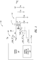
- FIG. 1 is a schematic diagram of an LLC resonant converter 100 including a control circuit 102 having time shift control circuitry 104 to provide time shift control (TSC) or symmetric time shift control (STSC) to control the operation of the resonant converter according to one embodiment of the present invention.
- STSC circuitry (not shown in Figure 1 ) in the time shift control circuitry 104 compensates for a lack of symmetry or "unbalance" in the detection of zero current crossings of a tank current I TANK generated during operation of the resonant converter 100.
- the detections of zero current crossings of the I TANK current are a necessary part of the time shift control (TSC) method of controlling resonant converters, as will be discussed in more detail below.
- the time shift control circuitry 104 eliminates unbalances in the detection of zero current crossings of the I TANK current by making symmetric times utilized in the time shift control of the resonant converter 100 that are based upon detection of these zero current crossings, as will also be explained in more detail below.
- the theory and overall operation of LLC resonant converters such as the LLC resonant converter 100 of Figure 1 is well understood by those skilled in the art, and thus will not be described in detail herein. Instead, the overall operation of the LLC resonant converter 100 will only briefly be described before describing in more detail the conventional time shift control method, which will then be followed by a detailed description of the symmetric time shift control of the resonant converter according to embodiments of the present invention.
- the primary side of the LLC resonant converter 100 includes a switching circuit 106, which is a half-bridge circuit formed by series-connected power switches Q1 and Q2 in the embodiment of Figure 1 .
- the switches Q1 and Q2 are power MOSFETs in the embodiment of Figure 1 and are coupled between a supply voltage node receiving a supply voltage VIN and a reference voltage node receiving a reference voltage, which is ground in the embodiment of Figure 1 .
- the control circuit 102 generates a high-side gate drive signal HSGD and a low-side gate drive signal LSGD to drive the gates of the switches Q1 and Q2, respectively, and thereby generates a phase voltage signal VHB on a phase node PH defined between the interconnection of the switches Q1 and Q2.
- the primary side of the LLC resonant converter 100 further includes a resonant circuit 108 coupled between the phase node PH and the reference node.
- This resonant circuit includes a series-connected resonant inductor Lr, a magnetizing inductance Lm of a transformer T and a resonant capacitor Cr.
- the secondary side of the LLC resonant converter 100 includes a rectification circuit 110 that rectifies an output current that is equal to the tank current I TANK , which is the resonant current in the resonant tank circuit 108, minus a current I Lm through the magnetizing inductance Lm to generate a DC output voltage VOUT on an output node OUT.
- the rectification circuit 110 includes two center tapped secondary windings S1 and S2 of the transformer T coupled to two diodes D1 and D2 as shown, with the center tap of these two secondary windings being coupled to the output node OUT.
- Figure 1 illustrates a primary model of the transformer T in which the contributions of all components in the transformer are related to or are with respect to the primary side of the transformer.
- the resonant inductor Lr and magnetizing inductance Lm represent both an inductance Lp of a primary winding and inductances LS1 and LS2 of the secondary windings S1, S2 of the transformer T, and the transformer has a turns ratio n':1 instead of a turns ratio n:1 of an ideal transformer, as will be appreciated by those skilled in the art.
- the rectification circuit 110 includes two diodes D1 and D2 in the embodiment of Figure 1 , in other embodiments the rectification includes, in place of these diodes, synchronous rectification switches such as MOSFETs and a synchronous rectification controller that controls the operation of these synchronous rectification switches, as will be appreciated by those skilled in the art.
- the resonant inductor Lr and magnetizing inductance Lm are integrated in a single transformer structure.
- the control circuit 102 controls the switching circuit 106 to generate the HSGD and LSGD signals in a complementary manner to drive the power switches Q1 and Q2 alternately with a fifty percent duty cycle for each power switch.
- the switching circuit 106 functions as a square wave generator to generate a square wave signal as the phase voltage signal VHB on the phase node PH.
- the resonant inductor Lr, capacitor Cr and magnetizing inductor Lm form the resonant circuit 108 and the fundamental frequency of the VHB signal generates a sinusoidal or piecewise sinusoidal resonant current or tank current I TANK in the resonant circuit.
- the frequency of the VHB signal thus determines the gain of the tank element and the generation of the output voltage VOUT.
- the control circuit 102 controls the switching circuit 106 to control the frequency of the generated VHB signal and thereby adjust the value of the generated output voltage VOUT.
- the transformer T is center tap transformer including the secondary windings S1 and S2. Transformer configurations other than center tap configurations may be used in further embodiments of the present invention.
- the rectification circuit 110 includes diodes D1 and D2 in the embodiment of Figure 1
- the rectification circuit similarly may have different structures in additional embodiments of the present invention.
- the transformer T is other than a center tap transformer
- the rectification circuit 110 may have a different structure.
- the rectification circuit 110 may have a different structure such as the inclusion of synchronous rectification switches in place of the diodes D1 and D2.
- FIG. 2 is a signal timing diagram showing the tank current I TANK and phase voltage signal VHB that would be generated according to conventional time shift control.
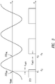
- Figure 3 is a signal timing diagram illustrating the effects of unbalanced or asymmetric operation in detecting zero current crossings under conventional time shift control of an LLC resonant converter as illustrated in Figure 2 .
- time shift control which may also be referred to as “the TSC method” or “TSC operation” in the present description
- the control circuitry of the resonant converter controls switching of the switching circuit (half-bridge or full-bridge circuit) based on a "time shift” or “time shift delay time” TD from a zero-current crossing (ZCC) of the tank current I TANK , which is detected by a zero-current detection (ZCD) comparator or circuit that detects these zero-current crossings of the tank current, as will be understood by those skilled in the art.
- ZCC zero-current crossing
- ZCD zero-current detection
- a switching cycle or period TSW of the phase voltage signal VHB corresponds to the time interval from a time t0 to a time t4.
- a TSC control circuit implementing the TSC control activates or drives high the VHB signal at the time t0 (i.e., the HSGD signal turns ON the switch Q1 a dead time DT (not shown in Figure 2 ) after the LSGD signal turns OFF switch Q2 in Figure 1 ), and the sinusoidal or approximately sinusoidal resonant or tank current I TANK continues increasing as seen in the figure.
- the dead time DT is a delay time between the turning OFF of the high side power switch Q1 and turning ON of the low side power switch Q2, and the turning OFF of switch Q2 and turning ON of switch Q1, as illustrated in Figure 4 and as will be discussed in more detail with reference to Figures 5 and 6 .
- a low-to-high zero-current crossing ZCC LH of the tank current I TANK occurs and is detected by the TSC control circuit of the resonant converter implementing the TSC method of control.
- the TSC control circuit toggles or switches the switching circuit to the complementary state, which in this situation corresponds to deactivating the VHB signal (e.g., driving the HSGD signal inactive to turn OFF the switch Q1 and driving the LSGD signal active to turn ON the switch Q2 in Figure 1 ).
- This deactivation of the VHB signal occurs a delay time TD after the detection of the zero-current crossing ZCC LH , which occurs at a time t2 in Figure 2 .
- the time t2 ideally occurs at one half of the switching cycle TSW or at a duration TSW/2 from the start of the switching cycle at the time t0.
- the TSC control circuit detects the zero-current crossing ZCC HL of the tank current I TANK and, in response to this detected zero current, the TSC control circuit again toggles or switches the switching circuit after the delay time TD to the complementary state.
- the complementary state corresponds to activating the VHB signal (e.g., driving the HSGD signal active to turn ON the switch Q1 and driving the LSGD signal inactive to turn OFF the switch Q2 in Figure 1 ).
- This activation of the VHB signal ideally occurs the delay time TD after the detection of the zero-current crossing ZCC HL at the time t4 in Figure 2 where the duration between the time t2 to time t4 is ideally equal to one half of the switching cycle TSW/2.
- Conventional TSC control is described in more detail in C. Adragna, D. Ciambellotti, M. Dell'Oro, F. Gallenda, "Digital Implementation and Performance Evaluation of a Time-Shift-Controlled LLC Resonant Half-Bridge Converter", 2014 IEEE Applied Power Electronics Conference and Exposition - APEC 2014, pp 2074-2080, 2014 .
- the TSC control circuitry implementing the TSC control includes a zero-current detection (ZCD) comparator for detecting these zero-current crossings ZCC of the tank current I TANK .
- the ZCD comparator generates a zero-current detection signal ZCD in response to detecting a zero-current crossing ZCC.
- ZCD zero-current detection
- the comparator typically exhibits unbalanced or asymmetric operational characteristics for the detection of the different types of zero-current crossings ZCC LH and ZCC HL .
- the ZCD comparator would detect each of these zero-current crossings ZCC and generate the ZCD signal in the identical way for each type of current crossing.
- This unbalanced or asymmetrical operation of the ZCD comparator manifests itself as a different delay between the occurrence of a zero-current crossing ZCC and the generation of the ZCD signal depending on type of zero-current crossing that has occurred.
- the detection of a zero-current crossing ZCC depends on the type of zero-current crossing that has occurred as seen in Figure 3 .
- Figure 3 shows the resonant current I TANK in the upper signal diagram and the ZCD signal generated by the ZCD comparator in the lower signal diagram.
- a low-to-high zero-current crossing ZCC LH occurs at a time t1 and, in response to this zero-current crossing, the ZCD comparator generates the ZCD signal a first delay time tdell later a time t2.
- a high-to-low zero-current crossing ZCC HL occurs a time t3 and, in response to this zero-current crossing, the ZCD comparator generates the ZCD signal a second delay time tdel2 later a time t4.
- the ZCD comparator When the operation of the ZCD comparator is unbalanced or asymmetric, these two delay times tdell and tdel2 are not equal as illustrate the figure, with the second delay time tdel2 being longer than the first delay time tdell in the example of Figure 3 .
- the ZCD comparator operates as if it has two different thresholds for the two different types of zero-current crossings ZCC. These unequal detection times exhibited by the ZCD comparator result in undesirable unbalanced or asymmetric operation of the LLC resonant converter.
- FIG. 4 is a signal timing diagram illustrating signals generated in the LLC resonant converter 100 of Figure 1 when the symmetric time shift control (STSC) circuitry 104 implements symmetric time shift control (STSC) according to one embodiment of the present invention.
- STSC symmetric time shift control
- This STSC control is based on the setting of the time shift of just one of the power switches Q1 or Q2 and then using the same total on time T ON , which is based on this time shift, for the other one of the power switches to thereby force symmetric operation of LLC resonant converter 100, as will be described in more detail below.
- This approach allows utilization of a smaller and less expensive ZCD comparator having less stringent trimming requirements.
- the on-time of the low side power switch Q2 is utilized in setting the time shift delay time TD that is utilized in switching both power switches Q1 and Q2.
- the on-time of the low side power switch Q2 T ONLS is equal to the sum of the delay time TD, a zero-current detection time T ZCD and other inherent delays in the operation of the LLC resonant converter 100.
- the value of the zero-current detection time T ZCD which corresponds to the occurrence of a high-to-low (i.e., negative going) zero-current crossing ZCC HL or low-to-high (i.e., positive going) zero-current crossing ZCC LH , can be different for the on-time T ONLS of the low side power switch Q2 and an on-time T ONHS of the high side power switch Q1.
- the on-time T ONLS of the low side power switch Q2 is detected and then the on-time T ONHS of the high side power switch Q1 is set to the same value as the low side on-time T ONLS .
- the same zero-current detection time T ZCD is used in the on-times T ONHS and T ONLS for the switches Q1 and Q2.
- the on-time T ONLS of the low side power switch Q2 is equal to the sum of the time shift time delay or T D being utilized by the control circuit 102 in the time shift control of the LLC resonant converter 100 plus a zero current detection time T ZCD to reach the next zero current crossing ZCC plus inherent delays T DEL (not shown in Figure 4 ) of components in the LLC resonant converter 100.
- T ONLS T D + T ZCD + T DEL and thus different zero current detection times T ZCD can cause different values for the on-times T ONLS and T ONHS .
- control circuitry 104 in eliminating this asymmetric operation by detecting the on-time T ONLS and then utilizing the same detected value for the on-time T ONHS in controlling the switching circuit 106 will now be described in more detail with reference to Figures 5 and 6 .
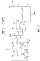
- FIG. 5 is a functional block diagram and schematic of the control circuitry 104 of Figure 1 according to one embodiment of the present invention.
- the control circuitry 104 can implement both conventional TSC control and STSC control according to embodiments of the present invention.
- the control circuitry 104 includes an output voltage sensing circuit 500 that senses the output voltage VOUT generated by the LLC resonant converter 100 and provides an input signal indicating the sensed output voltage to an optocoupler 502.
- the output voltage sensing circuit 500 calculates an error signal of the system indicating a difference between the generated value of the output voltage VOUT and a desired value of this output voltage. This error signal generated by the output voltage sensing circuit is supplied through the optocoupler 502 to the control circuitry 104.
- the resistors R1 and R2 function as a voltage divider to generate a divided voltage based on the output voltage VOUT.
- a shunt regulator SR receives the divided voltage and generates an output error voltage based on the divided voltage and thus on the output voltage. This output error voltage is supplied through the optocoupler 502 to the primary side.
- additional resistors R6, R4 along with resistor R1 and a capacitor C1 define a transfer function of the circuit and there define filtering characteristics of the circuit.
- the optocoupler 502 provides electrical isolation between the components of the output voltage sensing circuit 500 and other components on the secondary side of the LLC resonant converter 100 and the control circuitry 104 and other components on the primary side of the resonant converter. In response to the output voltage from the output voltage sensing circuit 500, the optocoupler 502 generates a feedback voltage VFB based on the value of the output voltage VOUT.
- Series connected resistors R7 and R8 are coupled between a logic supply voltage VCORE and a logic ground GND associated with the control circuit 102, and are coupled to bias the output of the optocoupler 502.
- a capacitor C3 is also coupled across the output of the optocoupler 502 to filter the generated feedback voltage VFB.
- the control circuitry 104 includes an analog-to-digital converter (ADC) 504 that converts the received analog feedback voltage VFB to a corresponding digital value VDFB and supplies this digitized value to core logic circuitry 506.
- ADC analog-to-digital converter
- the time shift delay time TD calculated by the core logic circuitry 506 is supplied to a finite state machine (FSM) 508 in the control circuitry 104 that utilizes this time shift in generating the LSGD and HSGD signals applied to control the switching of the high side power switch Q1 and low side power switch Q2 in the switching circuit 106 of Figure 1 .
- the FSM 508 generates the LSGD and HSGD signals to implement STSC control.
- the FSM 508 or other circuitry in the control circuitry104 can also implement conventional TSC control so that in this way the control circuitry 104 can implement either TSC control or STSC control in one embodiment of the present invention.
- the finite state machine 508 also receives the zero-current detection signal ZCD generated by the ZCD comparator 510 in the control circuitry 104.
- the ZCD comparator 510 has a first noninverting input coupled to reference voltage, which is ground in the embodiment of Figure 1 and is represented as a "0" in Figure 5 , while an inverting input of the comparator receives a signal indicating the value of the tank current I TANK in the resonant circuit 108.
- a current sensor S senses the tank current I TANK and supplies the sensed signal indicating or representative of the value of the tank current to the ZCD comparator 510 of Figure 5 .
- the ZCD comparator 510 then operates as previously described, namely the comparator generates the ZCD signal on its output based on the sensed I TANK current such that the ZCD signal indicates zero current crossings ZCC of the I TANK current in the resonant circuit 108.
- the finite state machine 508 In operation, the finite state machine 508 generates the LSGD and HSGD signals based upon the delay time TD from the core logic circuitry 506 and the ZCD signal from the ZCD comparator 510. In this way, the finite state machine 508 generates the LSGD and HSGD signals as previously described with reference to Figure 4 to control the switching of the power switches Q1 and Q2 in the switching circuit 106 of Figure 1 .
- Figure 6 is a state diagram illustrating the operation of the finite state machine 508 of Figure 5 in more detail according to one embodiment of the present invention. This more detailed operation of the finite state machine 508 in generating the LSGD and HSGD signals will now be described in more detail with reference to Figures 4 and 6 .
- the left-hand side of Figure 6 illustrates the operation of the finite state machine 508 in generating the HSGD signal to control the high side power switch Q1 while the right hand side illustrates the operation of the finite state machine in generating the LSGD signal to control the low side power switch Q2.
- the finite state machine 508 Upon initial power up or reset of the LLC resonant converter 100, the finite state machine 508 commences operation in a power-on-reset (POR) state 600 in which various parameters are set to initial values defining initial operation of the LLC resonant converter. From the POR state 600, the finite state machine 508 then enters a dead time state 602 associated with the LSGD and low side power switch Q2.
- POR power-on-reset
- the dead time DT is a delay time between the turning OFF of the high side power switch Q1 and turning ON of the low side power switch Q2, and turning OFF switch Q2 and turning ON switch Q1, as illustrated in Figure 4 and as will be appreciated by those skilled in the art.
- the finite state machine 508 After expiration of the dead time DT in the dead time state 602, the finite state machine 508 activates the LSGD signal to turn ON the low side power switch Q2 and then enters into a low side gate drive zero current detection state (LSGD ZCD STATE) 604. In the state 604, the finite state machine 508 waits for a transition of the ZCD signal from the ZCD comparator 510, which indicates a zero current crossing ZCC of the tank current I TANK has occurred and in this way detects the zero current detection time T ZCD for the low side power switch Q2. The finite state machine 508 saves this detected zero current detection time T ZCD as this same time will be used in controlling the high side power switch Q1, as will be described in more detail below.
- the finite state machine 508 may, for example, include a timer (not shown in Figure 5 ) that starts incrementing upon activation of the low side power switch Q2 after the dead time DT interval of state 602.
- the finite state machine 508 detects a transition of the ZCD signal, indicating such a zero current crossing ZCC, the count of the timer indicates the zero current detection time T ZCD .
- the finite state machine 508 may, of course, use approaches other than a timer to calculate or determine the time T ZCD .
- the finite state machine 508 transitions to a time shift state 606. In the time shift state 606, the finite state machine 508 times the delay time TD and thus the finite machine 508 stays in the time shift state until the time TD has elapsed.
- the finite state machine 508 Upon expiration of the time shift delay time TD, the finite state machine 508 then transitions from the time shift state 606 to a dead time state 608 associated with the HSGD signal and the high side power switch Q1.
- This dead time state 608 corresponds to the rightmost dead time DT indicated in Figure 4 , namely the dead time between deactivating the LSGD signal to turn OFF the low side power switch Q2 and activating the HSGD signal to turn ON the high side power switch Q1.
- the finite state machine 508 After expiration of the dead time DT in the dead time state 608, the finite state machine 508 then enters into a high side gate drive zero current detection state (HSGD ZCD STATE) 610 in which the finite state machine 508 does not wait for a transition of the ZCD signal from the ZCD comparator 510. Instead, the finite state machine 508 uses the time associated with a zero current crossing ZCC of the tank current I TANK as detected in the LSGD ZCD WAIT state 604 for the low side power switch Q2. This in represented as "dumper timer" arrow 612 in Figure 6 to indicate the zero current detection time T ZCD detected in state 604, or the count generated by the timer indicating this time, is used by the finite state machine 508 in the state 610.
- HSGD ZCD STATE high side gate drive zero current detection state
- the transition from the HSGD ZCD WAIT state 610 to TIME SHIFT state 614 does not depend on the ZCD signal generated by the ZCD comparator 510 but instead this transition from state 610 to state 614 depends on the duration of time T ZCD the LSGD ZCD WAIT state 604 has detected and then transferred or "dumped" to the state 610 for use in controlling the on time of the high side power switch Q1.
- the detection of the zero current crossing ZCC in the LSGD ZCD WAIT state 604 corresponds to the detection of the time T ZCD in Figure 4 as previously discussed, and thus this same time is used in the HSGD ZCD WAIT state 610 instead of basing the duration or time T ZCD of the state 610 on the ZCD signal from the comparator 610.
- the finite state machine 508 makes the on time of the high side power switch Q1 equal to the on time of the low side power switch Q2 as indicated in by the arrow 400 in Figure 4 .
- the finite state machine 508 Upon expiration of the dumped time (i.e., the time T ZCD detected in state 604), the finite state machine 508 transitions from state 610 to time shift state 614. In the time shift state 614, the finite state machine 508 again times the time shift delay time TD just as in the state 606, and thus the finite machine stays in the time shift state 614 until the time TD has elapsed. Upon expiration of the time TD in the state 614, the finite state machine 508 transitions again to the state 602. The finite state machine 508 continues this operation, alternately operating in states 602-606 and states 608-614 to control the operation of the low side and high side power switches Q2 and Q1, respectively. In this way, the same time T ZCD is used for control of the low side and high side switches Q2 and Q1 and the control of these switches is thus "symmetric," which is the reason this control has been referred to as symmetric time shift control in the present application.
- Embodiments of the present application are not limited to the example embodiments of Figures 4-6 .
- the approach is reversed, namely the on-time T ONHS of the high side power switch Q1 could be detected and then used to set the on-time T ONLS of the low side power switch Q2.
- the switching circuit is not a half-bridge circuit but is a full-bridge circuit or other suitable type of switching circuit.
- the on-time of one of the switching states of the switching circuit 106 is detected and then used in controlling the other switching states of the switching circuit according to embodiments of the present invention.
- the finite state machine can be formed from one or more of hardware, software and firmware, as will be appreciated by those skilled in the art. Where the finite state machine 508 is implemented purely in hardware, this hardware can also be formed purely from analog circuitry, purely from digital circuitry, or from a combination of both digital and analog circuitry.
- the entire control circuit 104, which includes the finite state machine 508, may similarly be formed from one or more of hardware, software and firmware, and where implemented purely in hardware this hardware may include purely analog circuitry, purely digital circuitry, or a combination of both digital and analog circuitry.
- FIG 7 is a graph illustrating unbalanced gain as a function of frequency that may be present in LLC resonant converters utilizing conventional time shift control, as will now be explained in more detail with reference to rectification circuit 110 of Figure 1 .
- An LLC resonant converter is required to operate at a 50% duty cycle to balance the currents through the output rectification diodes D1 and D2.
- Unbalances may result from mismatched delays in the drivers of converter, mismatches in operation of an oscillator (not shown) that is part of the control circuitry of a conventional LLC resonant converter, and, in the case of the resonant converter being controlled through time shift control, mismatches or unbalanced operation in delay or offset the ZCD comparator that detect zero current crossings of the tank current I TANK in the resonant circuit 108.
- the on-time of each of the drivers is determined by the sum of the time shift delay time TD, the time to reach current zero crossing in the form of the detected zero current detection time T ZCD , and delays in the system TDEL, as previously discussed.
- Any unbalance in the on-times causes an asymmetry in the tank current I TANK , the time T ZCD during high side on and low side operation on can be different and either increase or decrease the effect of a delay unbalance.
- the time shift control is amplifying the timing unbalances in the converter. This includes asymmetries or unbalances coming from both the ZCD comparator and from the drivers or oscillator components in the resonant converter.
- the time shift control method in fact adds, when compared to the direct frequency control method previously discussed, one more source of asymmetry or unbalance to the operation of the resonant converter, namely the ZCD comparator itself.
- the graph shows that for high loads (i.e., increasing output power Pout of the resonant converter along the horizontal axis) and above resonance, the time shift control tends to soften the effects of the asymmetries in the system, improving the balance of the tank current I TANK on the output windings S1, S2 ( Figure 1 ). Conversely, for low output power Pout or light loads, especially below resonance, the asymmetries can be strongly amplified, up to the point where only one output winding S1, S2 is delivering all the output current.
- the graphs of Figure 7 are based on a system having a resonant frequency of 50 kHz.
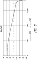
- FIG 8 is graph showing the loop gain of an LLC resonant converter using conventional time shift control and the loop gain of such a converter using symmetric time shift control according to embodiments of the present invention. Loop gain is shown on the vertical axis and frequency on the horizontal axis.
- the STSC control method differs from the TSC control method only for the calculation of the high side on time T ONHS and thus the dynamic behavior of the resonant converter implementing STSC control would be expected to be similar to that of a converter implementing TSC control, at least at low to medium frequencies.
- closed loop models of both a TSC and a STSC converter system were developed and loop gain was simulated as shown in Figure 8 . As seen in this figure, the loop gains are very similar and thus symmetric time shift control, as implemented in the LLC resonant converter 100 of Figure 1 as described above, does not adversely affect the loop gain of the converter.
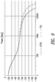
- Figure 9 is graph showing the phase shift of an LLC resonant converter as a function frequency using conventional time shift control and the phase shift of such a converter using symmetric time shift control.
- Figure 9 shows for the phase shift, just as Figure 8 does for the loop gain, that the gain and the phase of the resonant converter are essentially the same, at least at low to medium frequencies, for both TSC and STSC control methods.
- Both gain and phase characteristics with STSC control are still single pole systems, as is true for TSC control, except with STSC control the curves drop off at a slightly lower frequency as seen on the right hand side of each graph.
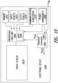
- FIG 10 is a functional block diagram of an electronic device 1000 including a resonant power converter 1002, such as the LLC resonant converter 100 of Figure 1 , that implements symmetric time shift control according to a further embodiment of the present invention.
- the electronic device 1000 in the example embodiment of Figure 11 includes processing circuitry 1004 that controls the overall operation of the electronic device 1000 and also executes applications or "apps" 1006 that provide specific functionality for a user of the electronic device.
- the resonant converter 1002 generates an output voltage Vout from an input voltage VIN supplied to the electronic device 1000.
- the input voltage VIN may be an AC voltage that is then rectified or may be a DC input voltage from an external power supply (not shown in Figure 10 ).
- the electronic device 1000 may be any type of electronic device, such as a smart phone, a tablet computer, a laptop computer, and so on.
- a power management subsystem 1008 of the electronic device 1000 is coupled to the processing circuitry 1004 and would typically include a battery for powering the electronic device, and also control circuitry for controlling power-related operating modes of the device such as charging of the battery, power-savings modes, and so on.
- the output voltage Vout generated by the voltage converter 1002 is supplied to the power management subsystem 1008 and other components in the electronic device 1000 as required.
- the electronic device 1000 further includes a video component such as a touch screen 1010 with a touch display (not shown) such as a liquid crystal display (LCD) and a touch panel (not shown) attached to or formed as an integral part of the touch display.
- the touch screen 1010 senses touches of a user of the electronic device 100 and provides sensed touch information to the processing circuitry 1004 to thereby allow the user to interface with and control the operation of the electronic device.
- the processing circuitry 1004 also controls the touch screen 1010 to display desired visual content on the touch display portion of the touch screen.
- the electronic device 1000 further includes data storage or memory 1012 coupled to the processing circuitry 1004 for storing and retrieving data including the apps 1006 and other software executing on the processing circuitry and utilized by the electronic device 1000 during operation.
- Examples of typical types of memory 1012 include solid state memory such as DRAM, SRAM and FLASH, solid state drives (SSDs), and may include any other types of memory suited to the desired functionality of the electronic device 1000 including digital video disks (DVDs), compact disk read-only (CD-ROMs), compact disk read-write (CD-RW) memories, magnetic tape, hard and floppy magnetic disks, tape cassettes, and so on.
- Input devices 1014 are coupled to the processing circuitry 1004 and may include a keypad, whether implemented through the touch screen 1010 or separately, a pressure sensor, accelerometer, microphone, keyboard, mouse, digital camera to capture still and video images, and other suitable input devices.
- Output devices 1016 are also coupled to the processing circuitry 1004 and may include, for example, audio output devices such as a speaker, printer, vibration device, and so on.
- the input devices 1014 and output devices 1016 collectively may include other types of typical communications ports for the electronic device 1000, such as USB ports, HDMI ports, and so on.
- the electronic device 1000 further includes communications subsystems 1018 coupled to the processing circuitry 1004 and which may include Wi-Fi, GPS, cellular and Bluetooth subsystems for providing the device with the corresponding functionality.
- the specific type and number of input devices 1014, output devices 1016, communications subsystems 1018, and even the specific functionality of the power management subsystem 1008 will of course depend on the type of the electronic device 1000.
Landscapes
- Engineering & Computer Science (AREA)
- Power Engineering (AREA)
- Dc-Dc Converters (AREA)
Claims (17)
- Steuerkreis (102), der zur Steuerung eines Schaltkreises (106) eines Resonanzwandlers (100) konfiguriert ist, der Schaltkreis schließt einen ersten Netzschalters (Q1) und einen zweiten Netzschalters (Q2) ein, die mit einem Resonanzkreis (108) gekoppelt sind, wobei der Steuerkreis konfiguriert ist, um eine erste Einschaltzeit (TONHS) des ersten Netzschalters und eine zweite Einschaltzeit (TONLS) des zweiten Netzschalters (Q2) zu steuern, um ein Rechtecksignal (VHB) zum Ansteuern des Resonanzkreises (108) zu erzeugen, der Steuerkreis (102) ist konfiguriert, um die erste Einschaltzeit zu steuern, basierend auf einer Nulldurchgang-Erfassungszeit (TZCD), die die Erkennung eines Stromnulldurchgangs eines Resonanzstroms (ITANK) anzeigt, der im Resonanzkreis (108) als Reaktion auf das Rechtecksignal (VHB) erzeugt wurde, und auf einer Zeitverschiebungsverzögerung (TD), die auf einer Ausgangsspannung (Vout) des Resonanzwandlers (100) basiert, dadurch gekennzeichnet, dass der Steuerkreis weiter konfiguriert ist, um die zweite Einschaltzeit des zweiten Netzschalters (Q2) zu steuern, basierend auf der für den ersten Netzschalter (Q1) erfassten Nulldurchgang-Erfassungszeit und der Zeitverschiebungsverzögerungszeit.
- Steuerkreis nach Anspruch 1, ferner umfassend einen Nulldurchgang-Erkennungskomparator (510), der mit dem Resonanzkreis (108) gekoppelt ist und konfiguriert, um Stromnulldurchgänge des Resonanzstroms (ITANK) zu erfassen und ein Nulldurchgang-Erkennungssignal basierend auf den erfassten Stromnulldurchgängen zu erzeugen.
- Steuerkreis nach Anspruch 2, ferner umfassend einen Zustandsautomaten (508), der mit dem Nulldurchgang-Erkennungskomparator (510) gekoppelt ist, um das Nulldurchgang-Erkennungssignal zu empfangen und gekoppelt, um die Zeitverschiebungsverzögerungszeit zu empfangen, wobei der Zustandsautomat (508) konfiguriert ist, um die ersten und zweiten Einschaltzeiten des ersten und zweiten Netzschalters zu steuern, basierend auf dem Nulldurchgang-Erkennungssignal und der Zeitverschiebungsverzögerungszeit.
- Steuerkreis nach Anspruch 3, wobei der Zustandsautomat (508) ferner konfiguriert ist, um die Einschaltzeit des ersten Netzschalters (Q1) zu steuern, indem zuerst eine Totzeit (DT), entsprechend einer Zeit zwischen einem Ausschalten des zweiten Netzschalters (Q2) und einem Einschalten des ersten Netzschalters (Q1), zeitlich festgelegt wird, und nach Ablauf der Totzeit den ersten Netzschalter einzuschalten, nach dem Einschalten des ersten Netzschalters, um einen Stromnulldurchgang des Resonanzstroms (ITANK) zu erfassen und um die Nulldurchgang-Erfassungszeit (TZCD) basierend auf dem erfassten Stromnulldurchgang zu bestimmen, und um die bestimmte Nulldurchgang-Erfassungszeit zu speichern und die Zeitverschiebungsverzögerungszeit zu verzögern, den erkannten Stromnulldurchgang zu ändern und den ersten Netzschalter (Q1) nach Ablauf der Zeitverschiebungsverzögerungszeit auszuschalten.
- Steuerkreis nach Anspruch 4, wobei der Zustandsautomat (508) ferner konfiguriert ist, um die Einschaltzeit des zweiten Netzschalters zu steuern, indem zuerst eine Totzeit, entsprechend einer Zeit zwischen einem Ausschalten des ersten Netzschalters (Q1) und einem Einschalten des zweiten Netzschalters (Q2), zeitlich festgelegt wird, und nach Ablauf der Totzeit den zweiten Netzschalter einzuschalten, nach dem Einschalten des zweiten Netzschalters (Q2), um die erfasste Nulldurchgang-Erfassungszeit einzustellen, und, nach Ablauf der erfassten Nulldurchgang-Erfassungszeit, um die Zeitverschiebungsverzögerungszeit nach Ablauf der Nulldurchgang-Erfassungszeit zu verzögern und den zweiten Netzschalter (Q2) nach Ablauf der Zeitverschiebungsverzögerungszeit auszuschalten.
- Steuerkreis nach Anspruch 4 oder 5, wobei der Zustandsautomat (508) einen Timer umfasst, um einen Zählwert zu erzeugen, der die erfasste Nulldurchgang-Erfassungszeit anzeigt.
- Steuerkreis nach einem der Ansprüche 1 bis 6, wobei der Schaltkreis (106) eine Halbbrückenschaltung umfasst, einschließlich einen durch den ersten Netzschalter (Q1) gebildeten High-Side-Netzschalter und einen durch den zweiten Netzschalter (Q2) gebildeten Low-Side-Netzschalter, wobei jeder der Low-Side- und High-Side-Netzschalter vorzugsweise einen MOSFET umfasst.
- Steuerkreis nach einem der Ansprüche 4 bis 7, ferner umfassend:einen Optokoppler (502) mit einem Eingang, der mit einem Ausgangsknoten des Resonanzwandlers (100) gekoppelt ist und konfiguriert, um ein optisches Signal basierend auf der Ausgangsspannung zu erzeugen und ein elektrisches Rückkopplungsspannungssignal (VFB) basierend auf dem erzeugten optischen Signal zu erzeugen;einen Analog-Digital-Umsetzer (ADC 504), der mit dem Optokoppler (502) gekoppelt ist, um das elektrische Rückkopplungsspannungssignal zu empfangen und das elektrische Rückkopplungsspannungssignal in einen digitalen Rückkopplungsspannungswert (VDFB) umzuwandeln; undeine mit dem Analog-Digital-Umsetzer (ADC 504) gekoppelte Kernfunktionsschaltung (506), um die digitale Rückkopplungsspannung zu empfangen und die Zeitverschiebungsverzögerungszeit basierend auf dem digitalen Rückkopplungsspannungswert zu erzeugen.
- Steuerkreis nach einem der Ansprüche 1 bis 8, wobei der Resonanzkreis (108) zwei induktive Elemente (L) und ein kapazitives Element (C) umfasst, die in Reihe geschaltet sind, so dass der Resonanzwandler (100) einen LLC-Resonanzwandler umfasst.
- Resonanzwandler, umfassend:Halbbrückenschaltung mit ersten und zweiten Netzschaltern (Q1, Q2) und einem Phasenknoten (PH), der an einer Verbindung des ersten und zweiten Netzschalters definiert ist;einen Resonanzkreis (108) mit einem Transformator (T) mit einer Primärseite und einer Sekundärseite, wobei die Primärseite mit dem Resonanzkreis gekoppelt ist;eine Gleichrichterschaltung (110), die mit der Sekundärseite des Transformators gekoppelt ist und mit einem Ausgangsknoten (OUT) gekoppelt ist; undden Steuerkreis nach einem der Ansprüche 1 bis 9.
- Resonanzwandler nach Anspruch 10, wobei der Transformator (T) eine Wicklung (Lm) in der Primärseite enthält, die ein induktives Resonanzelement des Resonanzkreises (108) bildet.
- Resonanzwandler nach Anspruch 10 oder 11, wobei der Resonanzkreis ferner einen Resonanzinduktor (Lr) umfasst, der mit der Wicklung in der Primärseite des Transformators (T) gekoppelt ist.
- Verfahren zum Steuern eines Resonanzwandlers (100), umfassend:Steuern von Einschaltzeiten (TONHS, TONLS) und Ausschaltzeiten des ersten und zweiten Netzschalters (Q1, Q2), um einen Resonanzkreis (108) anzusteuern, um einen Resonanzstrom (ITANK) im Resonanzkreis zu erzeugen;Erzeugen einer Ausgangsspannung (Vout) basierend auf dem Resonanzstrom im Resonanzkreis;Steuern einer ersten Einschaltzeit des ersten Netzschalters (Q1) basierend auf einer Nulldurchgang-Erfassungszeit (TZCD), die einen Stromnulldurchgang des Resonanzstroms anzeigt und auf einer Zeitverschiebungsverzögerungszeit (To) basiert, die auf der Ausgangsspannung (VOUT) basiert und Steuern einer zweiten Einschaltzeit des zweiten Netzschalters (Q2) basierend auf der für den ersten Netzschalter erfassten Nulldurchgang-Erfassungszeit und der Zeitverschiebungsverzögerungszeit.
- Verfahren nach Anspruch 13, ferner umfassend:
Erkennen von Stromnulldurchgängen des Resonanzstroms, Steuern der Einschaltzeit (TONHS) des ersten Netzschalters (Q1) durch:zeitliche Festlegung einer Totzeit (DT) entsprechend einer Zeit zwischen einem Ausschalten des zweiten Netzschalters und einem Einschalten des ersten Netzschalters,Einschalten des ersten Netzschalters nach Ablauf der Totzeit,Erfassen eines Stromnulldurchgangs des Resonanzstroms nach dem Einschalten des ersten Netzschalters,Bestimmen der Nulldurchgang-Erfassungszeit basierend auf dem erfassten Stromnulldurchgang,Speichern der bestimmten Nulldurchgang-Erfassungszeit,Verzögern der Zeitverschiebungsverzögerungszeit (To) nach dem erfassten Stromnulldurchgang, undAusschalten des ersten Netzschalters nach Ablauf der Zeitverschiebungsverzögerungszeit. - Verfahren nach Anspruch 14, ferner umfassend:
Steuerung der Einschaltzeit (TONLS) des zweiten Netzschalters (Q2) durch:zeitliche Festlegung einer Totzeit entsprechend einer Zeit zwischen einem Ausschalten des ersten Netzschalters und einem Einschalten des zweiten Netzschalters,Einschalten des zweiten Netzschalters nach Ablauf der Totzeit,zeitliche Festlegung der zuvor gespeicherten erfassten Nulldurchgang-Erfassungszeit nach dem Einschalten des zweiten Netzschalters,Verzögern der Zeitverschiebungsverzögerungszeit nach Ablauf der Nulldurchgang-Erfassungszeit, undAusschalten des zweiten Netzschalters nach Ablauf der Zeitverschiebungsverzögerungszeit. - Verfahren nach einem der Ansprüche 13 bis 15, wobei das Erzeugen der Ausgangsspannung basierend auf dem Resonanzstrom im Resonanzkreis Gleichrichtersignale umfasst, die als Reaktion auf den Resonanzstrom im Resonanzkreis erzeugt wurden.
- Verfahren nach einem der Ansprüche 13 bis 16, ferner umfassend das Erzeugen der Zeitverschiebungsverzögerungszeit basierend auf der Ausgangsspannung.
Applications Claiming Priority (1)
| Application Number | Priority Date | Filing Date | Title |
|---|---|---|---|
| US15/399,335 US10686382B2 (en) | 2017-01-05 | 2017-01-05 | Symmetric time shift control for resonant converters |
Publications (2)
| Publication Number | Publication Date |
|---|---|
| EP3346596A1 EP3346596A1 (de) | 2018-07-11 |
| EP3346596B1 true EP3346596B1 (de) | 2021-11-03 |
Family
ID=59699600
Family Applications (1)
| Application Number | Title | Priority Date | Filing Date |
|---|---|---|---|
| EP17187750.9A Active EP3346596B1 (de) | 2017-01-05 | 2017-08-24 | Symmetrische zeitverschiebungssteuerung für resonanzwandler |
Country Status (3)
| Country | Link |
|---|---|
| US (1) | US10686382B2 (de) |
| EP (1) | EP3346596B1 (de) |
| CN (2) | CN108282088B (de) |
Families Citing this family (20)
| Publication number | Priority date | Publication date | Assignee | Title |
|---|---|---|---|---|
| CN106877672A (zh) * | 2017-03-13 | 2017-06-20 | 成都芯源系统有限公司 | 谐振变换器及其方法 |
| JP2018174648A (ja) * | 2017-03-31 | 2018-11-08 | オムロン株式会社 | Llc共振コンバータ |
| CN108923657B (zh) * | 2018-07-02 | 2020-06-09 | 杭州茂力半导体技术有限公司 | 谐振变换器及其控制电路和控制方法 |
| DE102018116883A1 (de) * | 2018-07-12 | 2020-01-16 | Infineon Technologies Austria Ag | Sperrwandlersteuerung, Sperrwandler und Verfahren zum Betreiben des Sperrwandlers |
| EP3624319A1 (de) * | 2018-09-14 | 2020-03-18 | Delta Electronics (Thailand) Public Co., Ltd. | Schalterschutz |
| CN109391163B (zh) * | 2018-11-13 | 2020-12-01 | 深圳创维-Rgb电子有限公司 | 一种llc开关电源和显示装置 |
| US11316375B2 (en) * | 2019-08-26 | 2022-04-26 | Witricity Corporation | Control of active rectification in wireless power systems |
| US11509228B2 (en) * | 2019-10-17 | 2022-11-22 | Infineon Technologies Austria Ag | Dynamic regulation resonant power converter |
| WO2021217622A1 (zh) | 2020-04-30 | 2021-11-04 | 华为数字能源技术有限公司 | 一种电力电子变压器及供电系统 |
| KR102413538B1 (ko) * | 2020-05-08 | 2022-06-27 | 인투코어테크놀로지 주식회사 | 정밀하게 주파수를 제어하기 위한 주파수 제어 방법 및 이를 이용하는 주파수 제어 장치 |
| CN111796140B (zh) * | 2020-06-30 | 2023-06-30 | 上海宏力达信息技术股份有限公司 | 一种同时检测过零点和停复电的检测电路 |
| TWI747535B (zh) * | 2020-09-30 | 2021-11-21 | 台達電子工業股份有限公司 | Llc諧振轉換器、控制單元及其控制方法 |
| JP7676847B2 (ja) * | 2021-03-17 | 2025-05-15 | 富士電機株式会社 | スイッチング制御回路、共振型コンバータ |
| CN113364263B (zh) * | 2021-06-30 | 2023-07-04 | 深圳市辰久科技有限公司 | 死区产生电路及装置 |
| CN116430111B (zh) * | 2021-12-30 | 2025-12-05 | 台达电子工业股份有限公司 | 功率检测电路以及控制电路 |
| DE112023002903T5 (de) * | 2022-06-30 | 2025-04-17 | Microchip Technology Incorporated | Pwm zum steuern eines llc-leistungswandlers |
| CN115940650A (zh) * | 2022-11-03 | 2023-04-07 | 上海联影医疗科技股份有限公司 | 谐振变换装置的控制方法、谐振变换装置和镀膜电源 |
| US12388360B2 (en) * | 2023-02-22 | 2025-08-12 | Stmicroelectronics International N.V. | Charge control for resonant converters |
| CN118100655A (zh) * | 2023-12-19 | 2024-05-28 | 浙江艾罗网络能源技术股份有限公司 | 移相控制电路和llc电路的移相控制方法 |
| CN119853127B (zh) * | 2025-03-13 | 2025-08-01 | 深圳市润诚达电力科技有限公司 | 交直流充电桩双向功率流控制方法、装置及设备 |
Family Cites Families (13)
| Publication number | Priority date | Publication date | Assignee | Title |
|---|---|---|---|---|
| US5073849A (en) | 1988-12-20 | 1991-12-17 | Power-One, Inc. | Resonant DC to DC converter switching at zero current |
| KR101602474B1 (ko) * | 2009-03-05 | 2016-03-10 | 페어차일드코리아반도체 주식회사 | 보호 회로, 이를 포함하는 공진형 컨버터 및 그 보호 방법 |
| EP2309632B1 (de) | 2009-10-12 | 2013-05-29 | STMicroelectronics Srl | Steuervorrichtung für einen Halbbrücken-Resonanzwandler |
| IT1397087B1 (it) * | 2009-12-28 | 2012-12-28 | St Microelectronics Srl | Dispositivo di controllo in modalità a controllo di carica per un convertitore risonante. |
| EP2339734A1 (de) | 2009-12-28 | 2011-06-29 | STMicroelectronics S.r.l. | Gerät zur Kontrolle des Ladevorgangs für einen Resonzkonverter |
| JP5842366B2 (ja) * | 2011-04-04 | 2016-01-13 | 富士電機株式会社 | スイッチング電源制御回路 |
| CN102201754B (zh) | 2011-04-26 | 2014-03-12 | 刘闯 | 多电平逆变器的拓扑及恒频电压滞环控制 |
| US9166481B1 (en) | 2013-03-14 | 2015-10-20 | Vlt, Inc. | Digital control of resonant power converters |
| KR20140116338A (ko) * | 2013-03-22 | 2014-10-02 | 페어차일드코리아반도체 주식회사 | 스위치 제어 회로, 이를 포함하는 전력 공급 장치 및 그 구동 방법 |
| KR20150095181A (ko) | 2014-02-11 | 2015-08-20 | 페어차일드코리아반도체 주식회사 | 공진형 컨버터 및 그 구동 방법 |
| WO2016026090A1 (en) * | 2014-08-19 | 2016-02-25 | Abbeydorney Holdings Ltd. | Driving circuit, lighting device and method of reducing power dissipation |
| US9787191B2 (en) * | 2015-07-08 | 2017-10-10 | Infineon Technologies Austria Ag | Converter with quasi-resonant mode of operation for supplying power to a load |
| JP6597239B2 (ja) * | 2015-12-01 | 2019-10-30 | 富士電機株式会社 | スイッチング電源装置 |
-
2017
- 2017-01-05 US US15/399,335 patent/US10686382B2/en active Active
- 2017-08-24 EP EP17187750.9A patent/EP3346596B1/de active Active
- 2017-08-31 CN CN201710776024.XA patent/CN108282088B/zh active Active
- 2017-08-31 CN CN201721109609.8U patent/CN208094441U/zh active Active
Also Published As
| Publication number | Publication date |
|---|---|
| CN108282088B (zh) | 2021-01-01 |
| US10686382B2 (en) | 2020-06-16 |
| EP3346596A1 (de) | 2018-07-11 |
| CN208094441U (zh) | 2018-11-13 |
| US20180191252A1 (en) | 2018-07-05 |
| CN108282088A (zh) | 2018-07-13 |
Similar Documents
| Publication | Publication Date | Title |
|---|---|---|
| EP3346596B1 (de) | Symmetrische zeitverschiebungssteuerung für resonanzwandler | |
| US8102679B2 (en) | Utilization of a multifunctional pin to control a switched-mode power converter | |
| US8913404B2 (en) | Constant voltage constant current control circuits and methods with improved load regulation | |
| CN110752750B (zh) | 谐振变换器及其控制电路和控制方法 | |
| US8553431B2 (en) | Switching power converter with load impedance detection | |
| CN111327204B (zh) | 用于在开关功率转换器中在模式转变之后控制开关驱动信号的装置和方法 | |
| US9525358B2 (en) | Resonant converter, control circuit and associated control method with adaptive dead-time adjustment | |
| US9647562B2 (en) | Power conversion with switch turn-off delay time compensation | |
| US7098632B2 (en) | Controller in a voltage mode buck converter for implementing a mode-switch function and an over-current protection by a multifunction pin and method thereof | |
| US10418901B2 (en) | Power converter and methods of controlling a power converter | |
| KR101505264B1 (ko) | 저부하 동작으로의 전력공급모드 전환을 위한 조절 | |
| US20120033453A1 (en) | Controller for a Resonant Switched-Mode Power Converter | |
| EP2707942B1 (de) | Schaltverzögerungssteuerung für ein schaltnetzteil | |
| CN111327196B (zh) | 在功率转换器中同步多个控制器 | |
| EP2144356A1 (de) | Abwärtswandlerschwellenerkennung für einen automatischen Impulsüberspringungsmodus | |
| US9515545B2 (en) | Power conversion with external parameter detection | |
| US11557960B1 (en) | Adaptive enable and disable for valley switching in a power factor correction boost converter | |
| WO2018097820A1 (en) | Switch control for resonant power converter | |
| US20100202167A1 (en) | Soft switching power converter with a variable switching frequency for improving operation and efficiency | |
| CN107078655A (zh) | 电力转换装置 | |
| JP3459143B2 (ja) | スイッチングコンバータにおける過負荷保護方法 | |
| JP5857702B2 (ja) | スイッチング電源装置 | |
| US12567803B2 (en) | Conversion control circuit for controlling a resonant power converter and control method thereof | |
| TWI908473B (zh) | 一種用於諧振轉換器之控制裝置、控制方法及其非暫態電腦可讀儲存媒介 | |
| US20250293608A1 (en) | Voltage conversion circuit with output current limitation and method thereof |
Legal Events
| Date | Code | Title | Description |
|---|---|---|---|
| PUAI | Public reference made under article 153(3) epc to a published international application that has entered the european phase |
Free format text: ORIGINAL CODE: 0009012 |
|
| STAA | Information on the status of an ep patent application or granted ep patent |
Free format text: STATUS: THE APPLICATION HAS BEEN PUBLISHED |
|
| AK | Designated contracting states |
Kind code of ref document: A1 Designated state(s): AL AT BE BG CH CY CZ DE DK EE ES FI FR GB GR HR HU IE IS IT LI LT LU LV MC MK MT NL NO PL PT RO RS SE SI SK SM TR |
|
| AX | Request for extension of the european patent |
Extension state: BA ME |
|
| STAA | Information on the status of an ep patent application or granted ep patent |
Free format text: STATUS: REQUEST FOR EXAMINATION WAS MADE |
|
| 17P | Request for examination filed |
Effective date: 20190110 |
|
| RBV | Designated contracting states (corrected) |
Designated state(s): AL AT BE BG CH CY CZ DE DK EE ES FI FR GB GR HR HU IE IS IT LI LT LU LV MC MK MT NL NO PL PT RO RS SE SI SK SM TR |
|
| REG | Reference to a national code |
Ref country code: DE Ref legal event code: R079 Ref document number: 602017048612 Country of ref document: DE Free format text: PREVIOUS MAIN CLASS: H02M0003335000 Ipc: H02M0001000000 |
|
| GRAP | Despatch of communication of intention to grant a patent |
Free format text: ORIGINAL CODE: EPIDOSNIGR1 |
|
| STAA | Information on the status of an ep patent application or granted ep patent |
Free format text: STATUS: GRANT OF PATENT IS INTENDED |
|
| RIC1 | Information provided on ipc code assigned before grant |
Ipc: H02M 1/00 20060101AFI20210429BHEP Ipc: H02M 3/335 20060101ALI20210429BHEP Ipc: H02M 3/337 20060101ALI20210429BHEP |
|
| INTG | Intention to grant announced |
Effective date: 20210531 |
|
| GRAS | Grant fee paid |
Free format text: ORIGINAL CODE: EPIDOSNIGR3 |
|
| GRAA | (expected) grant |
Free format text: ORIGINAL CODE: 0009210 |
|
| STAA | Information on the status of an ep patent application or granted ep patent |
Free format text: STATUS: THE PATENT HAS BEEN GRANTED |
|
| AK | Designated contracting states |
Kind code of ref document: B1 Designated state(s): AL AT BE BG CH CY CZ DE DK EE ES FI FR GB GR HR HU IE IS IT LI LT LU LV MC MK MT NL NO PL PT RO RS SE SI SK SM TR |
|
| REG | Reference to a national code |
Ref country code: GB Ref legal event code: FG4D |
|
| REG | Reference to a national code |
Ref country code: AT Ref legal event code: REF Ref document number: 1444879 Country of ref document: AT Kind code of ref document: T Effective date: 20211115 Ref country code: CH Ref legal event code: EP |
|
| REG | Reference to a national code |
Ref country code: DE Ref legal event code: R096 Ref document number: 602017048612 Country of ref document: DE |
|
| REG | Reference to a national code |
Ref country code: IE Ref legal event code: FG4D |
|
| REG | Reference to a national code |
Ref country code: LT Ref legal event code: MG9D |
|
| REG | Reference to a national code |
Ref country code: NL Ref legal event code: MP Effective date: 20211103 |
|
| REG | Reference to a national code |
Ref country code: AT Ref legal event code: MK05 Ref document number: 1444879 Country of ref document: AT Kind code of ref document: T Effective date: 20211103 |
|
| PG25 | Lapsed in a contracting state [announced via postgrant information from national office to epo] |
Ref country code: RS Free format text: LAPSE BECAUSE OF FAILURE TO SUBMIT A TRANSLATION OF THE DESCRIPTION OR TO PAY THE FEE WITHIN THE PRESCRIBED TIME-LIMIT Effective date: 20211103 Ref country code: LT Free format text: LAPSE BECAUSE OF FAILURE TO SUBMIT A TRANSLATION OF THE DESCRIPTION OR TO PAY THE FEE WITHIN THE PRESCRIBED TIME-LIMIT Effective date: 20211103 Ref country code: FI Free format text: LAPSE BECAUSE OF FAILURE TO SUBMIT A TRANSLATION OF THE DESCRIPTION OR TO PAY THE FEE WITHIN THE PRESCRIBED TIME-LIMIT Effective date: 20211103 Ref country code: BG Free format text: LAPSE BECAUSE OF FAILURE TO SUBMIT A TRANSLATION OF THE DESCRIPTION OR TO PAY THE FEE WITHIN THE PRESCRIBED TIME-LIMIT Effective date: 20220203 Ref country code: AT Free format text: LAPSE BECAUSE OF FAILURE TO SUBMIT A TRANSLATION OF THE DESCRIPTION OR TO PAY THE FEE WITHIN THE PRESCRIBED TIME-LIMIT Effective date: 20211103 |
|
| PG25 | Lapsed in a contracting state [announced via postgrant information from national office to epo] |
Ref country code: IS Free format text: LAPSE BECAUSE OF FAILURE TO SUBMIT A TRANSLATION OF THE DESCRIPTION OR TO PAY THE FEE WITHIN THE PRESCRIBED TIME-LIMIT Effective date: 20220303 Ref country code: SE Free format text: LAPSE BECAUSE OF FAILURE TO SUBMIT A TRANSLATION OF THE DESCRIPTION OR TO PAY THE FEE WITHIN THE PRESCRIBED TIME-LIMIT Effective date: 20211103 Ref country code: PT Free format text: LAPSE BECAUSE OF FAILURE TO SUBMIT A TRANSLATION OF THE DESCRIPTION OR TO PAY THE FEE WITHIN THE PRESCRIBED TIME-LIMIT Effective date: 20220303 Ref country code: PL Free format text: LAPSE BECAUSE OF FAILURE TO SUBMIT A TRANSLATION OF THE DESCRIPTION OR TO PAY THE FEE WITHIN THE PRESCRIBED TIME-LIMIT Effective date: 20211103 Ref country code: NO Free format text: LAPSE BECAUSE OF FAILURE TO SUBMIT A TRANSLATION OF THE DESCRIPTION OR TO PAY THE FEE WITHIN THE PRESCRIBED TIME-LIMIT Effective date: 20220203 Ref country code: NL Free format text: LAPSE BECAUSE OF FAILURE TO SUBMIT A TRANSLATION OF THE DESCRIPTION OR TO PAY THE FEE WITHIN THE PRESCRIBED TIME-LIMIT Effective date: 20211103 Ref country code: LV Free format text: LAPSE BECAUSE OF FAILURE TO SUBMIT A TRANSLATION OF THE DESCRIPTION OR TO PAY THE FEE WITHIN THE PRESCRIBED TIME-LIMIT Effective date: 20211103 Ref country code: HR Free format text: LAPSE BECAUSE OF FAILURE TO SUBMIT A TRANSLATION OF THE DESCRIPTION OR TO PAY THE FEE WITHIN THE PRESCRIBED TIME-LIMIT Effective date: 20211103 Ref country code: GR Free format text: LAPSE BECAUSE OF FAILURE TO SUBMIT A TRANSLATION OF THE DESCRIPTION OR TO PAY THE FEE WITHIN THE PRESCRIBED TIME-LIMIT Effective date: 20220204 Ref country code: ES Free format text: LAPSE BECAUSE OF FAILURE TO SUBMIT A TRANSLATION OF THE DESCRIPTION OR TO PAY THE FEE WITHIN THE PRESCRIBED TIME-LIMIT Effective date: 20211103 |
|
| PG25 | Lapsed in a contracting state [announced via postgrant information from national office to epo] |
Ref country code: SM Free format text: LAPSE BECAUSE OF FAILURE TO SUBMIT A TRANSLATION OF THE DESCRIPTION OR TO PAY THE FEE WITHIN THE PRESCRIBED TIME-LIMIT Effective date: 20211103 Ref country code: SK Free format text: LAPSE BECAUSE OF FAILURE TO SUBMIT A TRANSLATION OF THE DESCRIPTION OR TO PAY THE FEE WITHIN THE PRESCRIBED TIME-LIMIT Effective date: 20211103 Ref country code: RO Free format text: LAPSE BECAUSE OF FAILURE TO SUBMIT A TRANSLATION OF THE DESCRIPTION OR TO PAY THE FEE WITHIN THE PRESCRIBED TIME-LIMIT Effective date: 20211103 Ref country code: EE Free format text: LAPSE BECAUSE OF FAILURE TO SUBMIT A TRANSLATION OF THE DESCRIPTION OR TO PAY THE FEE WITHIN THE PRESCRIBED TIME-LIMIT Effective date: 20211103 Ref country code: DK Free format text: LAPSE BECAUSE OF FAILURE TO SUBMIT A TRANSLATION OF THE DESCRIPTION OR TO PAY THE FEE WITHIN THE PRESCRIBED TIME-LIMIT Effective date: 20211103 Ref country code: CZ Free format text: LAPSE BECAUSE OF FAILURE TO SUBMIT A TRANSLATION OF THE DESCRIPTION OR TO PAY THE FEE WITHIN THE PRESCRIBED TIME-LIMIT Effective date: 20211103 |
|
| REG | Reference to a national code |
Ref country code: DE Ref legal event code: R097 Ref document number: 602017048612 Country of ref document: DE |
|
| PLBE | No opposition filed within time limit |
Free format text: ORIGINAL CODE: 0009261 |
|
| STAA | Information on the status of an ep patent application or granted ep patent |
Free format text: STATUS: NO OPPOSITION FILED WITHIN TIME LIMIT |
|
| 26N | No opposition filed |
Effective date: 20220804 |
|
| PG25 | Lapsed in a contracting state [announced via postgrant information from national office to epo] |
Ref country code: AL Free format text: LAPSE BECAUSE OF FAILURE TO SUBMIT A TRANSLATION OF THE DESCRIPTION OR TO PAY THE FEE WITHIN THE PRESCRIBED TIME-LIMIT Effective date: 20211103 |
|
| PG25 | Lapsed in a contracting state [announced via postgrant information from national office to epo] |
Ref country code: SI Free format text: LAPSE BECAUSE OF FAILURE TO SUBMIT A TRANSLATION OF THE DESCRIPTION OR TO PAY THE FEE WITHIN THE PRESCRIBED TIME-LIMIT Effective date: 20211103 |
|
| PG25 | Lapsed in a contracting state [announced via postgrant information from national office to epo] |
Ref country code: MC Free format text: LAPSE BECAUSE OF FAILURE TO SUBMIT A TRANSLATION OF THE DESCRIPTION OR TO PAY THE FEE WITHIN THE PRESCRIBED TIME-LIMIT Effective date: 20211103 |
|
| REG | Reference to a national code |
Ref country code: CH Ref legal event code: PL |
|
| GBPC | Gb: european patent ceased through non-payment of renewal fee |
Effective date: 20220824 |
|
| PG25 | Lapsed in a contracting state [announced via postgrant information from national office to epo] |
Ref country code: LU Free format text: LAPSE BECAUSE OF NON-PAYMENT OF DUE FEES Effective date: 20220824 Ref country code: LI Free format text: LAPSE BECAUSE OF NON-PAYMENT OF DUE FEES Effective date: 20220831 Ref country code: CH Free format text: LAPSE BECAUSE OF NON-PAYMENT OF DUE FEES Effective date: 20220831 |
|
| REG | Reference to a national code |
Ref country code: BE Ref legal event code: MM Effective date: 20220831 |
|
| PG25 | Lapsed in a contracting state [announced via postgrant information from national office to epo] |
Ref country code: IT Free format text: LAPSE BECAUSE OF FAILURE TO SUBMIT A TRANSLATION OF THE DESCRIPTION OR TO PAY THE FEE WITHIN THE PRESCRIBED TIME-LIMIT Effective date: 20211103 |
|
| PG25 | Lapsed in a contracting state [announced via postgrant information from national office to epo] |
Ref country code: IE Free format text: LAPSE BECAUSE OF NON-PAYMENT OF DUE FEES Effective date: 20220824 Ref country code: FR Free format text: LAPSE BECAUSE OF NON-PAYMENT OF DUE FEES Effective date: 20220831 |
|
| PG25 | Lapsed in a contracting state [announced via postgrant information from national office to epo] |
Ref country code: BE Free format text: LAPSE BECAUSE OF NON-PAYMENT OF DUE FEES Effective date: 20220831 |
|
| PG25 | Lapsed in a contracting state [announced via postgrant information from national office to epo] |
Ref country code: GB Free format text: LAPSE BECAUSE OF NON-PAYMENT OF DUE FEES Effective date: 20220824 |
|
| PG25 | Lapsed in a contracting state [announced via postgrant information from national office to epo] |
Ref country code: HU Free format text: LAPSE BECAUSE OF FAILURE TO SUBMIT A TRANSLATION OF THE DESCRIPTION OR TO PAY THE FEE WITHIN THE PRESCRIBED TIME-LIMIT; INVALID AB INITIO Effective date: 20170824 |
|
| PG25 | Lapsed in a contracting state [announced via postgrant information from national office to epo] |
Ref country code: CY Free format text: LAPSE BECAUSE OF FAILURE TO SUBMIT A TRANSLATION OF THE DESCRIPTION OR TO PAY THE FEE WITHIN THE PRESCRIBED TIME-LIMIT Effective date: 20211103 |
|
| PG25 | Lapsed in a contracting state [announced via postgrant information from national office to epo] |
Ref country code: MK Free format text: LAPSE BECAUSE OF FAILURE TO SUBMIT A TRANSLATION OF THE DESCRIPTION OR TO PAY THE FEE WITHIN THE PRESCRIBED TIME-LIMIT Effective date: 20211103 |
|
| PG25 | Lapsed in a contracting state [announced via postgrant information from national office to epo] |
Ref country code: MT Free format text: LAPSE BECAUSE OF FAILURE TO SUBMIT A TRANSLATION OF THE DESCRIPTION OR TO PAY THE FEE WITHIN THE PRESCRIBED TIME-LIMIT Effective date: 20211103 |
|
| PGFP | Annual fee paid to national office [announced via postgrant information from national office to epo] |
Ref country code: DE Payment date: 20250724 Year of fee payment: 9 |
|
| PG25 | Lapsed in a contracting state [announced via postgrant information from national office to epo] |
Ref country code: TR Free format text: LAPSE BECAUSE OF FAILURE TO SUBMIT A TRANSLATION OF THE DESCRIPTION OR TO PAY THE FEE WITHIN THE PRESCRIBED TIME-LIMIT Effective date: 20211103 |