EP3348981A2 - Hochempfindlicher siliciumpiezoresistorkraftsensor - Google Patents
Hochempfindlicher siliciumpiezoresistorkraftsensor Download PDFInfo
- Publication number
- EP3348981A2 EP3348981A2 EP17206053.5A EP17206053A EP3348981A2 EP 3348981 A2 EP3348981 A2 EP 3348981A2 EP 17206053 A EP17206053 A EP 17206053A EP 3348981 A2 EP3348981 A2 EP 3348981A2
- Authority
- EP
- European Patent Office
- Prior art keywords
- slab
- sense
- elements
- force
- die
- Prior art date
- Legal status (The legal status is an assumption and is not a legal conclusion. Google has not performed a legal analysis and makes no representation as to the accuracy of the status listed.)
- Withdrawn
Links
Images



Classifications
-
- G—PHYSICS
- G01—MEASURING; TESTING
- G01L—MEASURING FORCE, STRESS, TORQUE, WORK, MECHANICAL POWER, MECHANICAL EFFICIENCY, OR FLUID PRESSURE
- G01L1/00—Measuring force or stress, in general
- G01L1/18—Measuring force or stress, in general using properties of piezo-resistive materials, i.e. materials of which the ohmic resistance varies according to changes in magnitude or direction of force applied to the material
-
- G—PHYSICS
- G01—MEASURING; TESTING
- G01L—MEASURING FORCE, STRESS, TORQUE, WORK, MECHANICAL POWER, MECHANICAL EFFICIENCY, OR FLUID PRESSURE
- G01L1/00—Measuring force or stress, in general
- G01L1/20—Measuring force or stress, in general by measuring variations in ohmic resistance of solid materials or of electrically-conductive fluids; by making use of electrokinetic cells, i.e. liquid-containing cells wherein an electrical potential is produced or varied upon the application of stress
- G01L1/22—Measuring force or stress, in general by measuring variations in ohmic resistance of solid materials or of electrically-conductive fluids; by making use of electrokinetic cells, i.e. liquid-containing cells wherein an electrical potential is produced or varied upon the application of stress using resistance strain gauges
- G01L1/2206—Special supports with preselected places to mount the resistance strain gauges; Mounting of supports
-
- G—PHYSICS
- G01—MEASURING; TESTING
- G01L—MEASURING FORCE, STRESS, TORQUE, WORK, MECHANICAL POWER, MECHANICAL EFFICIENCY, OR FLUID PRESSURE
- G01L1/00—Measuring force or stress, in general
- G01L1/20—Measuring force or stress, in general by measuring variations in ohmic resistance of solid materials or of electrically-conductive fluids; by making use of electrokinetic cells, i.e. liquid-containing cells wherein an electrical potential is produced or varied upon the application of stress
- G01L1/22—Measuring force or stress, in general by measuring variations in ohmic resistance of solid materials or of electrically-conductive fluids; by making use of electrokinetic cells, i.e. liquid-containing cells wherein an electrical potential is produced or varied upon the application of stress using resistance strain gauges
- G01L1/2287—Measuring force or stress, in general by measuring variations in ohmic resistance of solid materials or of electrically-conductive fluids; by making use of electrokinetic cells, i.e. liquid-containing cells wherein an electrical potential is produced or varied upon the application of stress using resistance strain gauges constructional details of the strain gauges
- G01L1/2293—Measuring force or stress, in general by measuring variations in ohmic resistance of solid materials or of electrically-conductive fluids; by making use of electrokinetic cells, i.e. liquid-containing cells wherein an electrical potential is produced or varied upon the application of stress using resistance strain gauges constructional details of the strain gauges of the semi-conductor type
Definitions
- Force sensors can be used to measure a force or a pressure.
- Various designs can be used and can rely on a displacement of a component or a stress-field applied to a stress-sensitive element or component to measure the presence of a force and/or an amount of the force present on the sensor.
- Force sensors can experience forces above their designed operating ranges (e.g., overforce situations), which can result in damage to the force sensors.
- a sense die may comprise a chip comprising a slab; one or more sense elements supported by the slab, wherein the ratio of the width of the slab to the distance between the one or more sense elements is at least 2/1; one or more bond pads supported by a first side of the chip, each of the one or more bond pads electrically coupled to at least one of the one or more sense elements; a structural frame disposed on the first side of the chip, wherein the structural frame is disposed at least partially about the slab; and one or more electrical contacts extending through the structural frame, wherein the one or more electrical contacts are electrically coupled to the one or more bond pads.
- a method of sensing a force using a sense die may comprise providing a sense die comprising a chip having a slab formed thereon; applying a force to the slab of the sense die; and determining the magnitude of the force applied to the slab via one or more sense elements attached to the slab, wherein the ratio of the width of the slab to the distance between the one or more sense elements is greater than approximately 2/1.
- a sense die may comprise a chip comprising a slab; an actuation element configured to contact the slab at or near the center of the slab, and configured to apply a force to the slab; and one or more sense elements supported by the slab, wherein the ratio of the width of the slab to the distance between the one or more sense elements is greater than approximately 2/1, and wherein the distance between the sense elements is centered on the contact point between the actuation element and the slab.
- component or feature may,” “can,” “could,” “should,” “would,” “preferably,” “possibly,” “typically,” “optionally,” “for example,” “often,” or “might” (or other such language) be included or have a characteristic, that particular component or feature is not required to be included or to have the characteristic. Such component or feature may be optionally included in some embodiments, or it may be excluded.
- Embodiments of the disclosure include systems and methods for improving the signal output from a sense die configured to detect force applied to the sense die.
- Embodiments of the disclosure may comprise piezoresistive elements unusually close to the center of the die, where the load-bearing actuation element makes contact to the die face. Through stress mapping of the surface of the sense die, it was discovered that there is a small localized area of very high signal-generating stress near the actuation element. When piezoresistive elements are implanted in this location, die sensitivities can be up to 100 times greater or higher than traditional locations for the piezoresistive elements.
- a slab die may have the advantage of significantly higher proof loads (i.e. higher overload protection), while at the same time reducing cost because it is no longer necessity to complete the anisotropic etch. Additionally, this method of positioning the piezoresistive elements may allow for a smaller die to be used, which may lower costs as well.
- Typical uses of piezoresistive elements position the piezoresistive elements at or near the center edge of a formed diaphragm.
- Typical force sensors may use a stress field that is relatively distant from the contact point between the actuation element and the sense die (or the load point).
- Embodiments of the disclosure may use a localized stress field very near the load point. This localized stress field may be much higher in magnitude than the typically used distant stress field, leading to higher die output for a given load.
- a technical benefit of the described method of positioning the piezoresistive elements may include much higher die output for a given load. Additionally, since a full wafer thickness may be used, no specifically-defined diaphragm is required, and therefore the proof load is significantly higher. Also, the costs of the sense die may be reduced because no etch steps are required to form a diaphragm, no specially patterned adhesive is required under the die (just a continuous layer rather than a "picture frame" pattern with an unsupported central area), and a smaller die can be used (costs are proportional to the size of a die, where even a 30% reduction is die side length may translates to a cost reduction of up to 50%). The same general design and orientation of the piezoresistive elements may be similar to a traditional pressure or force sensor, but the location of the piezoresistive elements may be adjusted.
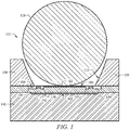
- FIG. 1 illustrates an embodiment of a typical sense die 100 according to some embodiments that can be used to detect a force, including a pressure.
- the sense die 100 can include a diaphragm or slab 102, and a substrate 140 located near a first surface 103 of the sensor.
- the slab 102 may comprise one or more sense elements 120, 124 connected to one or more electrical contacts 106.
- the sense elements 120, 124 may be located on a second surface 105 of the slab 102.
- a sidewall 108 can be attached to a portion of a second surface 105 of the sensor.
- An actuation element 110 can be present within a cavity 112 formed by the sidewall 108 and can serve to transfer a force to the second surface 105 of the slab 102.
- the slab 102 may comprise a solid slab.
- the slab 102 may be attached to the substrate 140 via an adhesive 142.
- the sense die 100 may be formed from silicon or other semiconductor material. While the sense die 100 is described with respect to being formed from silicon, it should be understood that other materials can also be used. In an embodiment, the sense die 100 can begin as a silicon chip and be processed to form the sense die 100, as described in more detail herein. In some embodiments, the silicon chip may include a recess formed on the first surface 103 to form a diaphragm 102. A variety of micro-fabrication techniques including, but not limited to, lithography techniques, wet etching techniques, and dry etching techniques may be used to form the recess.
- the diaphragm 102 may be fabricated on the sense die 100 by back-side etching of a silicon die (e.g., with a KOH etching technique, deep reactive ion etching, or other etching technique). However, it is contemplated that any suitable process may be used, as desired.
- the diaphragm 102 may have a height or thickness that is less than the thickness of the edges of the sense die 100, thereby forming the diaphragm 102.
- the diaphragm or slab 102 is configured to flex in response (or at least have some elastic response) to an applied force, creating stress fields that extend through the one or more sense elements 120 and 124, thereby allowing the applied force to be determined.
- the elastic response of the slab 102 may be microscopic in nature.
- the applied force can be present in the form of a differential pressure across the slab 102.
- an actuation element 110 may be in contact with the second surface 105 of the slab 102 to transfer a force to the slab 102.
- the actuation element 110 can comprise a mechanical coupling between an exterior force and the slab 102.
- the actuation element 110 can comprise a mechanical actuation element configured to transfer a force to the slab 102.
- the actuation element 110 may include a spherical object (such as the sphere shown in FIG. 1 ), a pin, an extender, a button, any other activation device, and/or a combination thereof.
- a spherical object such as the sphere shown in FIG. 1
- other types of actuators such as, for example, slidable mounted plungers or shafts, point of contact type components other than spherical objects, and/or "T"-shaped transfer mechanisms, in accordance with alternative embodiments.
- only a portion of an outer surface of the actuation element 110 may be spherical in shape or take on a particular shape.
- the actuation element 110 may be made of any material.
- the actuation element 110 may be formed from stainless steel, a polymer, a ceramic, jeweled, another suitable metal, and/or another suitable material.
- the actuation element 110 may include a stainless steel ball bearing. It is contemplated, however, that other generally spherical and other shaped elements may be used as or as part of the actuation element 110, if desired, including polymer based objects.
- the deflection resulting from a force applied on the diaphragm through an applied pressure and/or through the actuation element 110 may generally result in the deflection of the slab 102.
- the slab 102 may be configured to detect a deflection that is predominantly in a direction perpendicular to the plane of the slab 102.
- the sense die 100 is configured to measure a uniaxial force that is provided normal to the plane of sense die 100.
- the sense die 100 may have one or more sensing elements 120 and 124 disposed on or adjacent to the slab 102, such as piezoresistive sensing elements or components formed using suitable fabrication or printing techniques. For example, starting with the silicon sense die 100, standard pattern, implant, diffusion, and/or metal interconnect processes may be used to form one or more elements 120 and 124 on a surface 103, 105 of the sense die 100. For example, one or more piezoresistive sense elements 120 and 124 may be formed on the slab 102. The piezoresistive sense elements 120 and 124 may be configured to have an electrical resistance that varies according to an applied mechanical stress (e.g. deflection of the slab 102). The piezoresistive elements 120 and 124 can thus be used to convert the applied force or pressure into an electrical signal. In some instances, the piezoresistive components may include a silicon piezoresistive material; however, other non-silicon materials may be used.
- One or more bond pads 130 and 134 may be formed on the upper surface 105 of the sense die 100 and adjacent to the slab 102. Metal, diffusion, or other interconnects may be provided to interconnect the one or more piezoresistive sensor elements 120 and 124 and the one or more bond pads 130 and 134. As shown in FIG. 1 , one or more of the piezoresistive sensor elements 120 and 124 can be electrically coupled to one or more of the bond pads 130 and 134.
- the sense elements 120 and 124 may comprise a plurality of sense elements, for example two sense elements, three sense elements, four sense elements, or more.
- the bond pads 130 and 134 may comprise a plurality of bond pads, for example two bond pads, three bond pads, four bond pads, or more.
- FIG. 1 indicates typical locations for the piezoresistive elements 120 and 124. These locations may be selected to be within an area of the slab 102, where the slab 102 experiences forces from the contact with the actuation element 110.
- Embodiments of the disclosure describe a sense die 100 where the piezoresistive elements are located much closer to the contact area between the actuation element 110 and the slab 102 (or diaphragm), than a typical sense die.
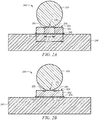
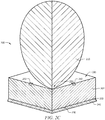
- FIGS. 2A-2C illustrate cross-sectional views of an actuation element 210 (which may comprise a ball bearing) and a slab 202 of a sense die 200.
- the actuation element 210 may comprise a spheroid shape.
- the actuation element 210 may contact and apply pressure to a contact area 220 between the actuation element 210 and the slab 202.
- the slab 202 may comprise a first surface 203, which may be attached to a structural frame 204.
- the slab 202 may comprise a second surface 205 configured to contact the actuation element 210.
- the actuation element 210 may comprise stainless steel. In some embodiments, the actuation element 210 may comprise glass, sapphire, or another similar material. In some embodiments, the total length of the sense die 200 may be reduced by approximately 20% to 30% compared to a typical sense die 200.
- FIG. 2A illustrates a sense die 200 comprising a slab 202 attached to a substrate 240 via an adhesive layer 242.
- the slab 202 may comprise sense elements 250 located on the surface 205 of the slab 202.
- the distance between the sense elements 250 is indicated by distance 260.
- the width of the slab 202 is indicated by width 262.
- the slab 202 may comprise an etched cavity 230 on the first surface 203 of the slab 202.
- the slab 202 may not be etched.
- the slab 202 may not comprise any thinned areas or cavities on either surface 203 and 205 of the slab 202.
- FIG. 2C illustrates a double cross-section of the slab 202, illustrating a quarter view of the slab 202 and actuation element 210.
- the slab 202 may comprise four sense element 250 located about the contact point 220 between the slab 202 and the actuation element 210.
- the sense elements 250 may be closer together than in a typical sense die. In some embodiments, the distance 260 between the sense elements 250 may be centered on the contact point 220 between the actuation element 210 and the slab 202.
- the ratio between the width 262 of the slab 202 and the distance 260 between the sense elements 250 may be greater than approximately 3/1. In some embodiments, the ratio between the width 262 of the slab 202 and the distance 260 between the sense elements 250 may be greater than approximately 5/1. In some embodiments, the ratio between the width 262 of the slab 202 and the distance 260 between the sense elements 250 may be greater than approximately 7/1. In some embodiments, the ratio between the width 262 of the slab 202 and the distance 260 between the sense elements 250 may be greater than approximately 11/1. In some embodiments, the ratio between the width 262 of the slab 202 and the distance 260 between the sense elements 250 may be less than approximately 20/1. In some embodiments, the sense elements 250 may not touch one another.
- the location of the sense elements 250 may be chosen based on the anticipated stress at a particular location on the surface 205 of the slab 202.
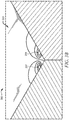
- a stress map 300 is shown illustrating the stress fields resulting from a force applied to the second surface 205 of the slab 202 by the actuation element 210.
- the slab 202 and actuation element 210 are shown above.
- the stress map 300 may comprise a plot of the difference between stress in the x direction (Sx) and stress in the y direction (Sy) or Sx-Sy. The largest values, both positive and negative, may indicate the locations on the surface 205 of the slab where the stress is the highest in one direction. These areas may be called "hotspots" or high stress areas.
- the stress field generated on the surface 205 at the hotspots 302 and 304 may be significantly greater than the stress field generated at other areas of the surface 205.
- the hotspots 302 and 304 may create an ideal location for a piezoresistive element to be placed on the surface 205, where the piezoresistive element may detect the stress created at that location.
- the hotspots 302 and 304 may be located closer to the contact area 220 than typical locations for piezoresistive elements.
- the stress map 300 shown in FIGS. 3A-3B may be cross-sectioned to show a quarter of the total surface 205 of the slab 202, wherein the corner 310 illustrates the center of the contact area 220 (as shown above) between the actuation element and the slab.
- a full stress map 300 may comprise up to four hotspots 302, 304, 306, and 308 surrounding the center 310 of the contact area 220 between the actuation element and the slab.
- the typical locations for piezoresistive elements are indicated by "x" 322, 324, 326, and 328.
- the piezoresistive elements (such as 120 and 124 described above) may be placed within one of the hotspots 302, 304, 306, and 308 indicated by the stress map 300. While the stress at the typical locations 322, 324, 326, and 328 for the piezoresistive elements may be within an area that will detect stress on the slab surface 205, the hotspots 302, 304, 306, and 308 may produce significantly higher outputs, thereby improving the accuracy and sensitivity of the piezoresistive elements.
- Sx-Sy stress at the typical locations 322, 324, 326, and 328 for piezoresistive elements may be approximately ⁇ 70 megapascal (MPa), and stress in the hotspots 302, 304, 306, and 308 may be approximately ⁇ 1400 MPa (approximately 20 times higher than the typical stress readings).
- the increased stress reading may produce an increased signal output for the piezoresistive elements.
- the Sx-Sy stress peak measured on the surface 205 of the slab moves outward radially from the contact area 220 as the load on the surface 205 is increased.
- the hotspots may change in location based on the magnitude of the force applied to the slab via the actuation element. For example, the distance from the center 310 at which the hotspot occurs may increase as the magnitude of the force increases. This concept may be illustrated by the following graphs and figures.
- Piezoresistive elements located at different positions with respect to the center of the surface 205 were evaluated at a range of forces applied to the surface 205.
- the results are show in the graphs of FIGS. 4A-4B .
- the locations ranged from approximately 39 microns ( ⁇ m) from the center to approximately 310 ⁇ m from the center.
- the sensor output in millivolts (mV) is plotted against the load applied to the slab in Newtons (N).
- N the load applied to the slab in Newtons
- Each line indicates a different location for the piezoresistive elements, measured in radians from the center of the contact area between the slab and the actuation element.
- the traditional location of the piezoresistive elements is also plotted, for reference, wherein the distance from the center is higher in a traditional sensor.
- the sensor output builds as the load increases until the Sx-Sy peak passes through the location of the piezoresistive element, and then then the output drops off. Sensor function may be optimal before the peak in the lines.
- the graph illustrates the results show in FIG. 4A that have been normalized using a standard of the traditional sensor location output (at a distance of 890 ⁇ m), where the results for each of the locations have been divided by the standard.
- the graph shown in FIG. 4B illustrates that the sensor output may be relatively constant before the peak (for that location), and may be usable for determining stress on the slab at that location.
- an optimal location for the piezoresistive elements may be chosen. For example, if the expected load is less than 5 N, the location for the piezoresistive elements may be chosen to be at a distance of between approximately 30 to 80 ⁇ m from the center. As another example, if the expected load is between 10 and 20 N, the location for the piezoresistive elements may be chosen to be at a distance of between approximately 100 to 120 ⁇ m from the center.
- an additional graph illustrates the approximate relationship between the contact radius between the flat surface of the slab and the curved surface of the spherical actuation element, and the estimated load that will be applied to the sense die.
- FIG. 5 is a plot of the radius of that circle of contact vs. force applied by the actuation element.
- the actuation element may contact one or more of the sense elements during the use life of the sense die.
- the signal from a piezoresistive element located at the typical location of 890 ⁇ m from the center may produce approximately 3.6 mV.
- the signal may rise to approximately 27.3 mV (approximately 7.6 times the typical output).
- the signal may rise to approximately 87.2 mV (approximately 246 times the typical output).
- the closer a piezoresistive element is location to the center i.e. the smaller the distance from the center
- the closest location for the piezoresistive element was approximately 150 ⁇ m from the center.
- the sensor output may be approximately 8.8 mV.
- piezoresistive elements positioned closer to the center of the slab may allow for improved signal output for lower force ranges.
- FIGS. 6A-6B further illustrate the relationship between the contact radius, i.e. the distance from the center 310 of the slab 202 at which the piezoresistive element is located, and the estimated load that will be applied to the sense die.
- the force applied to the actuation element 210 is approximately 25 N.
- the contact radius to the first hotspot 302 is indicated by distance 602.
- the contact radius to the second hotspot 304 is indicated by distance 604.
- the force applied to the actuation element 210 is increased to approximately 100 N.
- the distance 602 to the first hotspot 302 has increased accordingly.
- the distance 604 to the second hotspot 304 has increased accordingly. Therefore, the optimal location for the piezoresistive elements to be located at or near a hotspot 302 and 304 depends on the amount of force that is anticipated to be applied to the slab 202.
- the sensitivity ratio (when compared to a typical sensor) may be greater than approximately 1/1. In some embodiments, the sensitivity ratio may be greater than approximately 5/1. In some embodiments, the sensitivity ratio may be greater than approximately 10/1. In some embodiments, the sensitivity ratio may be greater than approximately 20/1. In some embodiments, the sensitivity ratio may be greater than approximately 25/1.
- a sense die may comprise a chip comprising a slab; one or more sense elements supported by the slab, wherein the ratio of the width of the slab to the distance between the one or more sense elements is at least 2/1; one or more bond pads supported by a first side of the chip, each of the one or more bond pads electrically coupled to at least one of the one or more sense elements; a structural frame disposed on the first side of the chip, wherein the structural frame is disposed at least partially about the slab; and one or more electrical contacts extending through the structural frame, wherein the one or more electrical contacts are electrically coupled to the one or more bond pads.
- a second embodiment can include the sense die of the first embodiment, wherein the sense elements comprise piezoresistive elements.
- a third embodiment can include the sense die of the first or second embodiments, further comprising an actuation element configured to contact the slab at or near the center of the slab.
- a fourth embodiment can include the sense die of the third embodiment, wherein the distance between the sense elements is centered on the contact point between the slab and the actuation element.
- a fifth embodiment can include the sense die of any of the first to fourth embodiments, wherein the ratio of the width of the slab to the distance between the one or more sense elements is greater than approximately 5/1.
- a sixth embodiment can include the sense die of any of the first to fifth embodiments, the ratio of the width of the slab to the distance between the one or more sense elements is greater than approximately 10/1.
- a seventh embodiment can include the sense die of any of the first to sixth embodiments, wherein the locations of the one or more sense elements are determined by mapping the force on the slab applied by the actuation element, and identifying one or more hotspots on the slab where the force is higher than the surrounding areas.
- An eighth embodiment can include the sense die of any of the first to seventh embodiments, wherein the locations of the one or more sense elements are determined by determining a correlation between the estimated force that will be applied to the slab and the desired location for sense elements on the slab.
- a method of sensing a force using a sense die may comprise providing a sense die comprising a chip having a slab formed thereon; applying a force to the slab of the sense die; and determining the magnitude of the force applied to the slab via one or more sense elements attached to the slab, wherein the ratio of the width of the slab to the distance between the one or more sense elements is greater than approximately 2/1.
- a tenth embodiment can include the method of the ninth embodiment, further comprising determining a correlation between the estimated force that will be applied to the slab and the desired location for sense elements on the slab.
- An eleventh embodiment can include the method of the tenth embodiment, wherein as the estimated force increases, the desired location for the sense elements increases in distance from the center of the slab.
- a twelfth embodiment can include the method in of any of the ninth to eleventh embodiments, wherein applying a force comprises contacting the slab with an actuation element.
- a thirteenth embodiment can include the method of the twelfth embodiment, wherein the distance between the sense elements is centered on the contact point between the slab and the actuation element.
- a fourteenth embodiment can include the method of any of the ninth to thirteenth embodiments, wherein the ratio of the width of the slab to the distance between the one or more sense elements is greater than approximately 5/1.
- a fifteenth embodiment can include the method of the any of the ninth to fourteenth embodiments, further comprising mapping the force on the slab applied by the actuation element; identifying one or more hotspots on the slab where the force is higher than the surrounding areas; and determining the location for a piezoresistive element to be located on the slab based on the location of the hotspots.
- a sense die may comprise a chip comprising a slab; an actuation element configured to contact the slab at or near the center of the slab, and configured to apply a force to the slab; and one or more sense elements supported by the slab, wherein the ratio of the width of the slab to the distance between the one or more sense elements is greater than approximately 2/1, and wherein the distance between the sense elements is centered on the contact point between the actuation element and the slab.
- a seventeenth embodiment can include the sense die of the sixteenth embodiment, wherein the sense elements comprise piezoresistive elements.
- An eighteenth embodiment can include the sense die of the sixteenth or seventeenth embodiments, wherein the ratio of the width of the slab to the distance between the one or more sense elements is greater than approximately 5/1.
- a nineteenth embodiment can include the sense die of any of the sixteenth to eighteenth embodiments, wherein the ratio of the width of the slab to the distance between the one or more sense elements is less than approximately 20/1.
- a twentieth embodiment can include the sense die of any of the sixteenth to nineteenth embodiments, wherein the sense elements are located at or near hotspots identified on the surface of the slab by force mapping.
Landscapes
- Physics & Mathematics (AREA)
- General Physics & Mathematics (AREA)
- Pressure Sensors (AREA)
- Force Measurement Appropriate To Specific Purposes (AREA)
Applications Claiming Priority (1)
| Application Number | Priority Date | Filing Date | Title |
|---|---|---|---|
| US15/388,483 US20180180494A1 (en) | 2016-12-22 | 2016-12-22 | High Sensitivity Silicon Piezoresistor Force Sensor |
Publications (2)
| Publication Number | Publication Date |
|---|---|
| EP3348981A2 true EP3348981A2 (de) | 2018-07-18 |
| EP3348981A3 EP3348981A3 (de) | 2018-10-03 |
Family
ID=60629545
Family Applications (1)
| Application Number | Title | Priority Date | Filing Date |
|---|---|---|---|
| EP17206053.5A Withdrawn EP3348981A3 (de) | 2016-12-22 | 2017-12-07 | Hochempfindlicher siliciumpiezoresistorkraftsensor |
Country Status (3)
| Country | Link |
|---|---|
| US (3) | US20180180494A1 (de) |
| EP (1) | EP3348981A3 (de) |
| CN (1) | CN108225626A (de) |
Families Citing this family (4)
| Publication number | Priority date | Publication date | Assignee | Title |
|---|---|---|---|---|
| US10794786B2 (en) | 2018-09-24 | 2020-10-06 | Honeywell International Inc. | Miniature size force sensor with bubble detection capabilities |
| US11156511B2 (en) | 2019-04-09 | 2021-10-26 | Honeywell International Inc. | Load cell |
| US11162850B2 (en) * | 2019-04-25 | 2021-11-02 | Measurement Specialties, Inc. | Sensor assemblies with integrated electrical connections and diaphragm overload protection |
| EP4302059B1 (de) * | 2021-03-01 | 2025-12-10 | Hahn-Schickard-Gesellschaft für angewandte Forschung e. V. | Vorrichtung zur messung von verformungen, spannungen, kräften und/oder drehmomenten in mehreren achsen |
Citations (1)
| Publication number | Priority date | Publication date | Assignee | Title |
|---|---|---|---|---|
| EP2270455A2 (de) * | 2009-07-02 | 2011-01-05 | Honeywell International Inc. | Kraftsensorvorrichtung |
Family Cites Families (60)
| Publication number | Priority date | Publication date | Assignee | Title |
|---|---|---|---|---|
| US3566216A (en) | 1968-08-07 | 1971-02-23 | Stow Lab Inc | An electromechanical transducer including a semiconductor and sensitivity controlling coupling means |
| US4050313A (en) * | 1975-06-04 | 1977-09-27 | Hitachi, Ltd. | Semiconductor pressure transducer |
| DE2809549C2 (de) * | 1977-03-07 | 1985-03-14 | Hitachi, Ltd., Tokio/Tokyo | Verfahren zur Herstellung eines Halbleiter-Druckmeßfühlers und Halbleiter-Druckmeßfühler |
| US4317126A (en) * | 1980-04-14 | 1982-02-23 | Motorola, Inc. | Silicon pressure sensor |
| JPS5780532A (en) * | 1980-11-07 | 1982-05-20 | Hitachi Ltd | Semiconductor load converter |
| JPS5952727A (ja) * | 1982-09-20 | 1984-03-27 | Hitachi Ltd | 半導体圧力センサ |
| US5178016A (en) * | 1989-11-15 | 1993-01-12 | Sensym, Incorporated | Silicon pressure sensor chip with a shear element on a sculptured diaphragm |
| DE4137624A1 (de) * | 1991-11-15 | 1993-05-19 | Bosch Gmbh Robert | Silizium-chip zur verwendung in einem kraftsensor |
| US5483994A (en) * | 1995-02-01 | 1996-01-16 | Honeywell, Inc. | Pressure transducer with media isolation and negative pressure measuring capability |
| US5644285A (en) | 1995-02-01 | 1997-07-01 | Honeywell Inc. | Pressure transducer with media isolation |
| JP3317084B2 (ja) | 1995-03-31 | 2002-08-19 | 株式会社豊田中央研究所 | 力検知素子およびその製造方法 |
| US5614678A (en) * | 1996-02-05 | 1997-03-25 | Kulite Semiconductor Products, Inc. | High pressure piezoresistive transducer |
| US5760313A (en) * | 1997-03-05 | 1998-06-02 | Honeywell Inc. | Force sensor with multiple piece actuation system |
| TW364092B (en) | 1997-04-04 | 1999-07-11 | Matsushita Electric Industrial Co Ltd | A load sensor and a pointing equipment incorporating the same |
| US5811694A (en) | 1997-06-06 | 1998-09-22 | Bokam Engineering | Force Transducer |
| JP4161410B2 (ja) * | 1997-07-25 | 2008-10-08 | 株式会社デンソー | 圧力検出装置 |
| US20040135274A1 (en) * | 1998-03-16 | 2004-07-15 | Shigenobu Matsuda | Microporous membrane |
| US6491647B1 (en) * | 1998-09-23 | 2002-12-10 | Active Signal Technologies, Inc. | Physiological sensing device |
| JP4843877B2 (ja) * | 2001-01-31 | 2011-12-21 | 株式会社デンソー | 半導体力学量センサ |
| JP3479064B1 (ja) * | 2002-04-12 | 2003-12-15 | 北陸電気工業株式会社 | 半導体力センサ |
| JP3915586B2 (ja) * | 2002-04-24 | 2007-05-16 | 株式会社デンソー | 力学量検出装置の製造方法 |
| JP2004279089A (ja) * | 2003-03-13 | 2004-10-07 | Denso Corp | 半導体圧力センサ |
| US7880247B2 (en) * | 2003-12-29 | 2011-02-01 | Vladimir Vaganov | Semiconductor input control device |
| US7521292B2 (en) * | 2004-06-04 | 2009-04-21 | The Board Of Trustees Of The University Of Illinois | Stretchable form of single crystal silicon for high performance electronics on rubber substrates |
| US7290453B2 (en) * | 2004-12-28 | 2007-11-06 | Amnon Brosh | Composite MEMS pressure sensor configuration |
| US7318349B2 (en) * | 2005-06-04 | 2008-01-15 | Vladimir Vaganov | Three-axis integrated MEMS accelerometer |
| US7467891B2 (en) * | 2005-11-29 | 2008-12-23 | Sensata Technologies, Inc. | Sensor arrangement for measuring a pressure and a temperature in a fluid |
| JP2007255953A (ja) | 2006-03-22 | 2007-10-04 | Hitachi Ltd | 力学量測定装置 |
| US7726197B2 (en) * | 2006-04-26 | 2010-06-01 | Honeywell International Inc. | Force sensor package and method of forming same |
| SG137708A1 (en) * | 2006-05-15 | 2007-12-28 | St Microelectronics Asia | Piezo-resistive force sensor with bumps on membrane structure |
| US7343812B2 (en) * | 2006-06-15 | 2008-03-18 | Honeywell International Inc. | Method to reduce die edge shorting on pressure sensors using conductive elastomeric seals |
| US7503221B2 (en) * | 2006-11-08 | 2009-03-17 | Honeywell International Inc. | Dual span absolute pressure sense die |
| JP4512125B2 (ja) | 2007-09-07 | 2010-07-28 | 株式会社リコー | 応力分布検出用半導体パッケージ群及びそれを用いた半導体パッケージの応力分布検出方法 |
| US7647842B1 (en) * | 2008-07-25 | 2010-01-19 | Honeywell International Inc. | Pressure-based fluid flow sensor |
| JP4810690B2 (ja) | 2008-11-11 | 2011-11-09 | 株式会社豊田中央研究所 | 力検知素子 |
| US8316725B2 (en) | 2010-12-15 | 2012-11-27 | Honeywell International Inc. | Force sensor |
| US9399572B2 (en) * | 2011-01-28 | 2016-07-26 | Elmos Semiconductor Ag | Microelectromechanical component and method for testing a microelectromechanical component |
| CA2806486C (en) * | 2011-02-07 | 2017-03-21 | The Governors Of The University Of Alberta | Piezoresistive load sensor |
| KR101273700B1 (ko) * | 2011-09-15 | 2013-06-12 | 삼성전기주식회사 | Mems 소자 |
| US9728652B2 (en) * | 2012-01-25 | 2017-08-08 | Infineon Technologies Ag | Sensor device and method |
| US9459162B2 (en) * | 2012-03-02 | 2016-10-04 | Hitachi, Ltd. | Device for measuring mechanical quantity |
| US8806964B2 (en) * | 2012-03-23 | 2014-08-19 | Honeywell International Inc. | Force sensor |
| US9003899B2 (en) * | 2012-03-23 | 2015-04-14 | Honeywell International Inc. | Force sensor |
| US9003897B2 (en) * | 2012-05-10 | 2015-04-14 | Honeywell International Inc. | Temperature compensated force sensor |
| US9032818B2 (en) * | 2012-07-05 | 2015-05-19 | Nextinput, Inc. | Microelectromechanical load sensor and methods of manufacturing the same |
| US8757001B2 (en) * | 2012-09-27 | 2014-06-24 | Honeywell International Inc. | Mechanically coupled force sensor on flexible platform assembly structure |
| US9164003B2 (en) * | 2012-10-11 | 2015-10-20 | Honeywell International Inc. | Force sensor with mechanical over-force transfer mechanism |
| EP2735855A1 (de) * | 2012-11-21 | 2014-05-28 | Sensata Technologies, Inc. | Messvorrichtung zur Messung einer physischen Menge |
| GB2515715A (en) | 2012-11-21 | 2015-01-07 | Continental Automotive Systems | Piezoresistive transducer with low thermal noise |
| US20140374848A1 (en) * | 2013-06-24 | 2014-12-25 | Wen Shi Koh | Semiconductor sensor device with metal lid |
| JP6226171B2 (ja) * | 2013-07-04 | 2017-11-08 | ローム株式会社 | 応力センサ |
| US9470593B2 (en) * | 2013-09-12 | 2016-10-18 | Honeywell International Inc. | Media isolated pressure sensor |
| US9383270B1 (en) * | 2013-10-28 | 2016-07-05 | Sandia Corporation | Silicon force sensor |
| WO2015065639A1 (en) * | 2013-10-30 | 2015-05-07 | Honeywell International Inc. | Force sensor with gap-controlled over-force protection |
| US9052246B2 (en) * | 2013-11-14 | 2015-06-09 | Honeywell International Inc. | Force sensor using integral force biasing for improved linearity |
| US10317297B2 (en) * | 2013-12-11 | 2019-06-11 | Melexis Technologies Nv | Semiconductor pressure sensor |
| JP6188231B2 (ja) | 2014-02-26 | 2017-08-30 | アルプス電気株式会社 | 荷重検出装置及び前記荷重検出装置を用いた電子機器 |
| JP6346279B2 (ja) * | 2014-06-27 | 2018-06-20 | 北陸電気工業株式会社 | 力検出器 |
| EP3236226B1 (de) * | 2016-04-20 | 2019-07-24 | Sensata Technologies, Inc. | Verfahren zur herstellung eines drucksensors |
| WO2017221762A1 (ja) * | 2016-06-23 | 2017-12-28 | 株式会社村田製作所 | 電気音響変換装置 |
-
2016
- 2016-12-22 US US15/388,483 patent/US20180180494A1/en not_active Abandoned
-
2017
- 2017-12-07 EP EP17206053.5A patent/EP3348981A3/de not_active Withdrawn
- 2017-12-21 CN CN201711392719.4A patent/CN108225626A/zh active Pending
-
2019
- 2019-09-17 US US16/573,500 patent/US11573136B2/en active Active
-
2023
- 2023-01-05 US US18/150,692 patent/US12474224B2/en active Active
Patent Citations (1)
| Publication number | Priority date | Publication date | Assignee | Title |
|---|---|---|---|---|
| EP2270455A2 (de) * | 2009-07-02 | 2011-01-05 | Honeywell International Inc. | Kraftsensorvorrichtung |
Also Published As
| Publication number | Publication date |
|---|---|
| US20230146578A1 (en) | 2023-05-11 |
| US20200033207A1 (en) | 2020-01-30 |
| US11573136B2 (en) | 2023-02-07 |
| US12474224B2 (en) | 2025-11-18 |
| US20180180494A1 (en) | 2018-06-28 |
| EP3348981A3 (de) | 2018-10-03 |
| CN108225626A (zh) | 2018-06-29 |
Similar Documents
| Publication | Publication Date | Title |
|---|---|---|
| US12474224B2 (en) | Silicon piezoresistor force sensor | |
| US8569092B2 (en) | Method for fabricating a microelectromechanical sensor with a piezoresistive type readout | |
| US20120297884A1 (en) | Device for measuring environmental forces and method of fabricating the same | |
| EP3012638B1 (de) | Silizium-membran drucksensor | |
| US10571348B2 (en) | Overforce control through sense die design | |
| CN107894294B (zh) | 带有扩展浅多边形腔的带腔绝缘体上硅mems压力传感装置 | |
| EP3376194B1 (de) | Mems kraftsensor mit kammer samt entlüftungskanälen | |
| JP2010203818A (ja) | 半導体センサ及びその製造方法 | |
| EP1712515A2 (de) | Technik zum Herstellen von mikroelektromechanischen Strukturen | |
| JP7508744B2 (ja) | 複数範囲構造を有するセンサ組立体 | |
| EP3580541B1 (de) | Mikrometerschnittstelle für mechanische kraft | |
| KR102234831B1 (ko) | 압력 센서 | |
| US9010200B2 (en) | Device for measuring forces and method of making the same | |
| US9964458B2 (en) | Pressure sensor device with anchors for die shrinkage and high sensitivity | |
| US20180067008A1 (en) | Buried cavity sense die diaphragm stop for force sensors | |
| JPH07113707A (ja) | 半導体複合機能センサ | |
| Baumann et al. | CMOS-based force sensor with overload protection and improved assembly tolerance | |
| JP2008045911A (ja) | 圧力センサ | |
| Jeong et al. | Wafer level packaged cantilever array type contact force sensor | |
| CN110207864A (zh) | 敏感膜和传力导杆一体化的微力传感器及其加工方法 | |
| JPH0694557A (ja) | 半導体圧力センサ |
Legal Events
| Date | Code | Title | Description |
|---|---|---|---|
| PUAI | Public reference made under article 153(3) epc to a published international application that has entered the european phase |
Free format text: ORIGINAL CODE: 0009012 |
|
| 17P | Request for examination filed |
Effective date: 20171207 |
|
| AK | Designated contracting states |
Kind code of ref document: A2 Designated state(s): AL AT BE BG CH CY CZ DE DK EE ES FI FR GB GR HR HU IE IS IT LI LT LU LV MC MK MT NL NO PL PT RO RS SE SI SK SM TR |
|
| AX | Request for extension of the european patent |
Extension state: BA ME |
|
| PUAL | Search report despatched |
Free format text: ORIGINAL CODE: 0009013 |
|
| AK | Designated contracting states |
Kind code of ref document: A3 Designated state(s): AL AT BE BG CH CY CZ DE DK EE ES FI FR GB GR HR HU IE IS IT LI LT LU LV MC MK MT NL NO PL PT RO RS SE SI SK SM TR |
|
| AX | Request for extension of the european patent |
Extension state: BA ME |
|
| RIC1 | Information provided on ipc code assigned before grant |
Ipc: G01L 1/22 20060101ALI20180828BHEP Ipc: G01L 1/18 20060101AFI20180828BHEP |
|
| 17Q | First examination report despatched |
Effective date: 20190502 |
|
| STAA | Information on the status of an ep patent application or granted ep patent |
Free format text: STATUS: THE APPLICATION IS DEEMED TO BE WITHDRAWN |
|
| 18D | Application deemed to be withdrawn |
Effective date: 20190713 |