EP3349043A1 - Procédé de lecture d'un pixel de démodulation et capteur de distance - Google Patents
Procédé de lecture d'un pixel de démodulation et capteur de distance Download PDFInfo
- Publication number
- EP3349043A1 EP3349043A1 EP17151300.5A EP17151300A EP3349043A1 EP 3349043 A1 EP3349043 A1 EP 3349043A1 EP 17151300 A EP17151300 A EP 17151300A EP 3349043 A1 EP3349043 A1 EP 3349043A1
- Authority
- EP
- European Patent Office
- Prior art keywords
- potential
- floating diffusion
- charge carriers
- gates
- storage
- Prior art date
- Legal status (The legal status is an assumption and is not a legal conclusion. Google has not performed a legal analysis and makes no representation as to the accuracy of the status listed.)
- Granted
Links
Images




Classifications
-
- G—PHYSICS
- G01—MEASURING; TESTING
- G01S—RADIO DIRECTION-FINDING; RADIO NAVIGATION; DETERMINING DISTANCE OR VELOCITY BY USE OF RADIO WAVES; LOCATING OR PRESENCE-DETECTING BY USE OF THE REFLECTION OR RERADIATION OF RADIO WAVES; ANALOGOUS ARRANGEMENTS USING OTHER WAVES
- G01S7/00—Details of systems according to groups G01S13/00, G01S15/00, G01S17/00
- G01S7/48—Details of systems according to groups G01S13/00, G01S15/00, G01S17/00 of systems according to group G01S17/00
- G01S7/483—Details of pulse systems
- G01S7/486—Receivers
- G01S7/4861—Circuits for detection, sampling, integration or read-out
- G01S7/4863—Detector arrays, e.g. charge-transfer gates
-
- G—PHYSICS
- G01—MEASURING; TESTING
- G01S—RADIO DIRECTION-FINDING; RADIO NAVIGATION; DETERMINING DISTANCE OR VELOCITY BY USE OF RADIO WAVES; LOCATING OR PRESENCE-DETECTING BY USE OF THE REFLECTION OR RERADIATION OF RADIO WAVES; ANALOGOUS ARRANGEMENTS USING OTHER WAVES
- G01S17/00—Systems using the reflection or reradiation of electromagnetic waves other than radio waves, e.g. lidar systems
- G01S17/02—Systems using the reflection of electromagnetic waves other than radio waves
- G01S17/06—Systems determining position data of a target
- G01S17/08—Systems determining position data of a target for measuring distance only
- G01S17/32—Systems determining position data of a target for measuring distance only using transmission of continuous waves, whether amplitude-, frequency-, or phase-modulated, or unmodulated
-
- G—PHYSICS
- G01—MEASURING; TESTING
- G01S—RADIO DIRECTION-FINDING; RADIO NAVIGATION; DETERMINING DISTANCE OR VELOCITY BY USE OF RADIO WAVES; LOCATING OR PRESENCE-DETECTING BY USE OF THE REFLECTION OR RERADIATION OF RADIO WAVES; ANALOGOUS ARRANGEMENTS USING OTHER WAVES
- G01S17/00—Systems using the reflection or reradiation of electromagnetic waves other than radio waves, e.g. lidar systems
- G01S17/88—Lidar systems specially adapted for specific applications
- G01S17/89—Lidar systems specially adapted for specific applications for mapping or imaging
- G01S17/894—Three-dimensional [3D] imaging with simultaneous measurement of time-of-flight at a two-dimensional [2D] array of receiver pixels, e.g. time-of-flight cameras or flash lidar
-
- G—PHYSICS
- G01—MEASURING; TESTING
- G01S—RADIO DIRECTION-FINDING; RADIO NAVIGATION; DETERMINING DISTANCE OR VELOCITY BY USE OF RADIO WAVES; LOCATING OR PRESENCE-DETECTING BY USE OF THE REFLECTION OR RERADIATION OF RADIO WAVES; ANALOGOUS ARRANGEMENTS USING OTHER WAVES
- G01S7/00—Details of systems according to groups G01S13/00, G01S15/00, G01S17/00
- G01S7/48—Details of systems according to groups G01S13/00, G01S15/00, G01S17/00 of systems according to group G01S17/00
- G01S7/491—Details of non-pulse systems
- G01S7/4912—Receivers
- G01S7/4913—Circuits for detection, sampling, integration or read-out
-
- H—ELECTRICITY
- H10—SEMICONDUCTOR DEVICES; ELECTRIC SOLID-STATE DEVICES NOT OTHERWISE PROVIDED FOR
- H10F—INORGANIC SEMICONDUCTOR DEVICES SENSITIVE TO INFRARED RADIATION, LIGHT, ELECTROMAGNETIC RADIATION OF SHORTER WAVELENGTH OR CORPUSCULAR RADIATION
- H10F39/00—Integrated devices, or assemblies of multiple devices, comprising at least one element covered by group H10F30/00, e.g. radiation detectors comprising photodiode arrays
- H10F39/80—Constructional details of image sensors
- H10F39/803—Pixels having integrated switching, control, storage or amplification elements
Definitions
- the invention relates to a method for reading out a demodulation pixel according to the preamble of claim 1 and to a distance sensor according to the preamble of claim 10.
- MCT minimum charge transfer method
- the portion of an optical signal carrying the information to be transmitted is regularly superimposed by any background (background light, etc.).
- background background light, etc.
- the optical signal can first be recorded with two channels of a photodetector, with the incident photons inducing mobile charge carriers in the photodetector.
- the background component occurs in equal proportions in charge carrier groups divided into two channels, so that the difference between corresponding charge carrier quantities can be determined in order to eliminate this background component.
- the charge carriers can first be collected over a certain period of time in each case in a collection unit (storage gate).
- a second region for example a floating diffusion
- the respectively divided charge carrier quantities are thus trapped in the respective storage gates, so to speak in a potential well, while they are collected there.
- charge carriers can only flow out of a storage gate for floating diffusion with continuous change of the pot depth of the storage gates and then, with further reduction of the pot depth, from both. From the determinable potential differences, the difference of the two charge quantities results.
- the object of the invention is to be able to provide a method for reading out a demodulation pixel or a distance sensor, which enables faster processing.
- the method according to the invention is used to read out a demodulation pixel of a distance sensor which is used to determine the distance to an object.
- the difference between two charge carrier quantities can be determined independently of the total amount of charge quantities.
- demodulation pixels to receive the radiation: First of all, the received radiation is converted in a conversion region into photoinduced charge carriers. These charge carriers can be removed for further detection and processing from the corresponding conversion region, generally the bulk region of a lightly doped semiconductor material, for example by applying a voltage. These charge carriers can be divided alternately, namely given according to a modulation frequency, into at least two charge carrier quantities. Thus, phase characteristics of the detected light compared to the originally emitted light signal can also be determined via a temporal correlation.
- the divided charge carrier quantities are first each caught and collected in a potential well, each potential well being assigned to individual storage gates.
- This collection of charge carriers corresponds to a temporal integration.
- An edge of such a potential well of a storage gate is formed by a so-called transfer gate, which effectively acts as a lock between the storage gate and a floating diffusion.
- the charge carrier quantity can be measured in the respective floating diffusion.
- the pot depth of the corresponding storage gates is also changed. Both, namely the height of the potential wall and the pot depth of the storage gates can be changed simultaneously or at different times. Preferably, first the height of the potential barrier of the transfer gate and then the pot depth of the storage gates can be changed.
- the invention enables a particularly effective suppression of the background superimposed on the actual signal.
- the method according to the invention makes it possible to detect optical signals which, unlike the background which superimposes the signals, have a comparatively low intensity.
- carriers which are generated by, for example, a photodetector upon receiving an optical signal are transformed into e.g. split two different storage gates.
- the method according to the invention is applied to distance sensors, but the signal is split up in a temporal sequence, ie, in temporal succession, the photoinduced charge carriers are assigned to different collection units (storage gates).
- the respective periods in which the Carriers are assigned to the respective collection units (storage gates), are equal to each other.
- TOF sensors time of flight
- TOF time of flight
- the division of the charge carriers also takes place according to a modulation frequency.
- This modulation frequency is also the frequency which is superimposed on the emitted light signal in the case of the distance sensor operating as a TOF sensor in order finally to determine the distance. For example, a low-frequency signal compared to the light frequency is superimposed on the light pulse to be emitted, and finally the phase difference that results when the light travels a certain distance to an object and the reflected-back signal in the distance sensor is detected.
- the superimposed background may be, for example, a background light such as natural daylight / sunlight or light generated by a nearby lamp (common-mode background).
- the dark current for example, by charge carriers generated thermally in the semiconductor material of the sensor, can contribute to this. For this reason, it can also be assumed that the change of this light occurs, if at all, at much greater time intervals, at least in comparison with the period of the modulation frequency.
- the difference of two signals, in which photoinduced charge carriers are collected in time sequence is suitable for substantially eliminating the background.
- the integration times in which charge carriers are collected in the storage gates are in the microsecond or sub-microsecond range, while the changes in the background are often expected, if at all, only in the hourly range.
- such changes in the background light are usually at best continuous and not abrupt.
- the inventive method allows a much faster signal processing, because much lower capacity must be controlled.
- a variable control voltage can be applied to the transfer gate and thus the height of the potential barrier can be influenced:
- the potential wall of the transfer device provided had to have a finite height which was kept constant, thus Then, if the pot depth of the respective storage gates is reduced, there is also the possibility that the charge carriers overcome this potential wall of the respective transfer device in order finally to reach a detection area (floating diffusion).
- the pot depth of the respective Storage gates no longer changed and kept constant.
- the method according to the invention is characterized in that it can be implemented simply and does not require any fundamental changes to the detector layout previously used.
- Stopping the passage of the charge carriers to the respective associated floating diffusion can then take place as soon as charge carriers pass from two of the storage gates in each case. From the storage gate in which a larger amount of charge carriers has accumulated, charge carriers will first be able to pass to the corresponding floating diffusion, because in this case the potential wall of the transfer gate can be overcome more quickly. If the potential barrier is lowered further or the pot depth of the storage gates is reduced, charge carriers of the corresponding other storage gate will also be able to pass to the floating diffusion at a later point in time. Now at this time, the potential difference of the two floating diffusion can be determined, resulting in the difference of the charge carrier amounts. Advantageously, this determination can also be made independently of the total amount of charge carrier amounts, i. it can largely be disregarded how strong the background radiation is without the signal carrying the actual information having to be amplified beforehand.
- the potential barrier between storage gate and floating diffusion can be increased again in one embodiment of the invention, so that the transition of the charge carriers from the potential well of the storage gate for floating diffusion can be practically prevented, otherwise arrive at known from the prior art sensors charge carriers for floating diffusion, even if the pot depth of the Storage gates or the voltage applied to the storage gate control voltage is no longer changed.
- the potential wall of the transfer gate is very high in order to allow effective stopping of the charge carriers or retention of the charge carriers in the potential well .
- the pot depth of the storage gate or the control voltage of the storage gate is not even varied so much that the charge carriers are lifted to the level of the much higher potential barrier of the transfer gate. Only then, when the charge carriers are to transfer to the floating diffusion, the height of the potential barrier is lowered.
- a comparison device may be provided which compares the measured potential with a reference value, ie, for example, an operational amplifier (comparator) is provided, which firstly has the reference value potential and, secondly, the potential of the corresponding floating diffusion is connected.
- a reference value ie, for example, an operational amplifier (comparator) is provided, which firstly has the reference value potential and, secondly, the potential of the corresponding floating diffusion is connected.
- the height of the potential barrier of the transfer gate is first of all influenced or reduced. If no charge carriers have yet flowed to the floating diffusion during the lowering of the potential wall, this lowering of the potential wall is stopped at a predetermined time or at a given height of the potential wall (approximately at half of the maximum pot depth on the storage gate), the depth subsequently being the potential well of the storage gate is reduced (for this, the potential of the storage gate is lowered in the present circuit). This happens at least until correspondingly each charge carrier can overcome the potential barrier. Basically, it is also conceivable to simultaneously vary the height of the potential barrier and the depth of the potential well by the Control voltages of the transfer gate and the storage gate can be varied simultaneously.
- the advantage in terms of the control may be that the change in the potential barrier does not have to change the sign abruptly in terms of time. Otherwise, in order to allow the charge carriers to flow over the floating diffusion, the potential of the potential barrier would otherwise have to be lowered and, in order to stop this passage, it would have to be increased again immediately thereafter. This change of sign should be done comparatively abruptly. It is therefore advantageous if this last section, before the charge carriers exceed the potential barrier, is caused by a change in the control voltage of the storage gate, i. the depth of the potential well is reduced. For the sake of completeness, it should be mentioned that possible tunnel effects according to which a quantum-mechanical tunneling of charge carriers through a barrier is not or only conditionally considered in the present case.
- a corresponding separation region can be provided.
- the most effective conversion of the incident photons of the optical signal to be detected into photo-induced charge carriers may advantageously be provided in a large conversion region of sufficient thickness for deep penetrating photons.
- a large area of the bulk material is provided as a conversion area, such as a lightly doped area. This area also allows for large Penetration depth of the photons an effective transformation into charge carriers.
- the separation does not take place effectively in the entire, comparatively large conversion range, but the charge carriers are drawn off from there and fed to a separation region.
- This can be done advantageously by applying a voltage, for which purpose a so-called driftgate is provided in particular.
- driftgate is provided in particular.
- a distance sensor is characterized in that the transfer gates are designed to change the height of each of them generated potentials, further comprising a comparison device is provided to perform a lowering of the respective potential walls before or from two storage gates
- a comparison device is provided to perform a lowering of the respective potential walls before or from two storage gates
- an embodiment of the invention also allows a particularly compact design.
- an arrangement within a matrix of demodulation pixels in a distance sensor according to the invention can be designed in such a way that it can be read out in rows and columns. Defining a row and a column results in a one-to-one association with a specific pixel. The evaluation result of the common comparison device can thus be assigned exactly to this pixel.
- Such a design can be even more space-saving and compact, and further realized with lower cost.
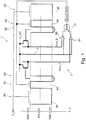
- FIG. 1 shows a schematic representation of a demodulation pixel 1.
- the conversion region in which the photoinduced charge carriers are generated by photons of a signal to be detected, as well as the actual semiconductor topography, are not shown in detail.
- the photoinduced charge carriers are separated according to a modulation frequency into two charge carrier quantities which are each collected over a certain time interval in the storage gates 2A, 2B.
- potential wells 3A, 3B are respectively formed in the storage gates 2A, 2B.
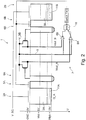
- the collection of charge carriers is in FIG. 2 shown.
- the two storage gates 2A, 2B in the actually selected semiconductor topography are each immediately adjacent to a drift gate, in the region of which the charge carriers are led out of the conversion area.
- a different order has been selected in the representation of the figures.
- One wall of the potential well 3A and 3B forms the potential barrier 4A and 4B, respectively, which in turn is generated by the transfer gate 5A, 5B.
- the potential wells 4A, 4B separate the potential wells 3A, 3B from the floating diffusion 6A, 6B, wherein the floating diffusion 6A, 6B respectively allow a potential measurement or a determination of the amounts of charge carriers flowed over to them.
- the two floating diffusion 6A, 6B are each connected to an input of an operational amplifier 8A, 8B.
- These two operational amplifiers 8A, 8B compare the applied voltage value with respect to a reference potential which is supplied via the Line 9 is connected as a common potential to both operational amplifiers 8A, 8B.
- the operational amplifiers 8A, 8B thus compare the respective potential of the floating diffusion 6A or 6B with a corresponding common reference potential (reference value) and provide a digital output "1" if this reference value is exceeded or the value "0" if the Reference value is not reached.
- FIG. 2 differs only from the according to FIG. 1 in that charge carrier quantities 11A, 11B are collected in the potential wells 3A, 3B. This means that, after a predetermined modulation frequency, charge carriers are alternately directed into the storage gate 2A and 2B, respectively.
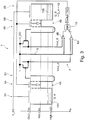
- FIG. 3 For reading the demodulation pixel, as shown FIG. 3 now the potential barriers 4A, 4B lowered. Incidentally, it can be seen that the charge carrier amount 11A is smaller than the charge carrier amount 11B.
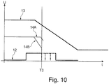
- the potential curve is in the diagram FIG. 4 shown, wherein the potential or the applied control voltage on the axis U and the time are plotted on the axis t.
- the voltage at the transfer gate 5A, 5B was respectively increased at the same time or the height of the corresponding potential walls 4A, 4B lowered, which in the diagram according to FIG. 4 is shown by a sudden increase of the curve 12 at time T0.
- the depth of the potential wells 3A, 3B is decreased ( FIG. 5 ) by also lowering the potential of the respective storage gates 2A, 2B.
- the corresponding reduction of the potential of the storage gates 2A, 2B is in the curve 13 from FIG. 6 shown.
- the potential of the curve 12 at this time still remains constant, ie the height of the potential walls 4A, 4B does not change for the time being.
- FIG. 7 it is shown in which for the first time charge carriers flow over from the charge carrier amount 11B in the direction of floating diffusion 6B. This is at the Charge amount 11B, which is greater than the charge carrier amount 11A over time thus earlier the case.
- FIG. 8 the two curves 14A, 14B of the floating diffusion 6A, 6B are shown, with the curve 14A correspondingly remaining constant, while the curve 14B has a potential dip at the point in time T2. The more charge carriers from one of the potential wells 3A, 3B flow over into the corresponding floating diffusion 6A, 6B, the lower the corresponding potential of the floating diffusion 6A, 6B becomes.
- FIG. 13 again shows a distance sensor or a matrix arrangement 20 of demodulation pixels 21.
- An enlarged representation of the wiring of a demodulation pixel is shown in FIG FIG. 14 shown.
- the order 20 runs in rows Z and columns S.
- FIG. 14 shows, for each demodulation pixel of a row Z common lines for the storage gates 2A, 2B (line 22) and for the reference potential (line 23) are provided line by line.
- a common line 24 is provided in order to apply the variable control voltage to the transfer gates 5A, 5B of a respective column S.
- the readout of the matrix 20 takes place in rows and columns, wherein the definition of a specific row Z or column S automatically determines a specific demodulation pixel 21.
- a variable control voltage can be applied to the transfer gates; There is a lowering of the respective potential ramps of the respective transfer gates before and / or until two of the storage gates each charge carriers can overcome the respective potential wall of the corresponding transfer gate and pass to the associated floating diffusion. In particular, the stopping of the charge carrier flow for floating diffusion can be stopped more abruptly and effectively. Overall, the signal processing time can be reduced.
Landscapes
- Engineering & Computer Science (AREA)
- Physics & Mathematics (AREA)
- Computer Networks & Wireless Communication (AREA)
- General Physics & Mathematics (AREA)
- Radar, Positioning & Navigation (AREA)
- Remote Sensing (AREA)
- Electromagnetism (AREA)
- Solid State Image Pick-Up Elements (AREA)
- Optical Radar Systems And Details Thereof (AREA)
Priority Applications (2)
| Application Number | Priority Date | Filing Date | Title |
|---|---|---|---|
| EP17151300.5A EP3349043B1 (fr) | 2017-01-13 | 2017-01-13 | Procédé de lecture d'un pixel de démodulation et capteur de distance |
| US15/857,827 US10845483B2 (en) | 2017-01-13 | 2017-12-29 | Method for reading a demodulation pixel and distance sensor |
Applications Claiming Priority (1)
| Application Number | Priority Date | Filing Date | Title |
|---|---|---|---|
| EP17151300.5A EP3349043B1 (fr) | 2017-01-13 | 2017-01-13 | Procédé de lecture d'un pixel de démodulation et capteur de distance |
Publications (2)
| Publication Number | Publication Date |
|---|---|
| EP3349043A1 true EP3349043A1 (fr) | 2018-07-18 |
| EP3349043B1 EP3349043B1 (fr) | 2022-01-05 |
Family
ID=57796225
Family Applications (1)
| Application Number | Title | Priority Date | Filing Date |
|---|---|---|---|
| EP17151300.5A Active EP3349043B1 (fr) | 2017-01-13 | 2017-01-13 | Procédé de lecture d'un pixel de démodulation et capteur de distance |
Country Status (2)
| Country | Link |
|---|---|
| US (1) | US10845483B2 (fr) |
| EP (1) | EP3349043B1 (fr) |
Cited By (1)
| Publication number | Priority date | Publication date | Assignee | Title |
|---|---|---|---|---|
| CN113424071A (zh) * | 2019-02-15 | 2021-09-21 | 新唐科技日本株式会社 | 摄像装置以及距离信息算出方法 |
Families Citing this family (1)
| Publication number | Priority date | Publication date | Assignee | Title |
|---|---|---|---|---|
| CN112118368B (zh) * | 2019-06-04 | 2021-08-24 | 宁波飞芯电子科技有限公司 | 栅压调节电路、栅压调节方法及应用其的传感器 |
Citations (4)
| Publication number | Priority date | Publication date | Assignee | Title |
|---|---|---|---|---|
| US20080079833A1 (en) * | 2006-09-29 | 2008-04-03 | Brainvision Inc. | Solid-state image sensor |
| EP2187237A1 (fr) * | 2007-08-22 | 2010-05-19 | Hamamatsu Photonics K.K. | Dispositif d'imagerie à semi-conducteurs et dispositif de mesure d'image de distance |
| WO2010144616A1 (fr) | 2009-06-09 | 2010-12-16 | Mesa Imaging Ag | Système de soustraction d'électron de domaine de charge dans des pixels de démodulation et procédé afférent |
| EP2743724A1 (fr) * | 2012-12-12 | 2014-06-18 | Espros Photonics AG | Capteur de distance TOF et procédé de fonctionnement |
-
2017
- 2017-01-13 EP EP17151300.5A patent/EP3349043B1/fr active Active
- 2017-12-29 US US15/857,827 patent/US10845483B2/en active Active
Patent Citations (4)
| Publication number | Priority date | Publication date | Assignee | Title |
|---|---|---|---|---|
| US20080079833A1 (en) * | 2006-09-29 | 2008-04-03 | Brainvision Inc. | Solid-state image sensor |
| EP2187237A1 (fr) * | 2007-08-22 | 2010-05-19 | Hamamatsu Photonics K.K. | Dispositif d'imagerie à semi-conducteurs et dispositif de mesure d'image de distance |
| WO2010144616A1 (fr) | 2009-06-09 | 2010-12-16 | Mesa Imaging Ag | Système de soustraction d'électron de domaine de charge dans des pixels de démodulation et procédé afférent |
| EP2743724A1 (fr) * | 2012-12-12 | 2014-06-18 | Espros Photonics AG | Capteur de distance TOF et procédé de fonctionnement |
Cited By (1)
| Publication number | Priority date | Publication date | Assignee | Title |
|---|---|---|---|---|
| CN113424071A (zh) * | 2019-02-15 | 2021-09-21 | 新唐科技日本株式会社 | 摄像装置以及距离信息算出方法 |
Also Published As
| Publication number | Publication date |
|---|---|
| US20180203117A1 (en) | 2018-07-19 |
| US10845483B2 (en) | 2020-11-24 |
| EP3349043B1 (fr) | 2022-01-05 |
Similar Documents
| Publication | Publication Date | Title |
|---|---|---|
| DE102013225676B4 (de) | Lichtlaufzeitkamera mit einer Bewegungserkennung | |
| DE19737330C2 (de) | Abbildungssystem und Verfahren zum Betreiben desselben | |
| EP0517303B1 (fr) | Arrangement avec une matrice de détecteurs et un dispositif de remise en zéro | |
| DE2622828C3 (de) | Verfahren zum Betreiben von BiIdfühlern | |
| DE60319228T2 (de) | Lichtempfangsvorrichtung mit regelbarer empfindlichkeit und gerät zur detektion der räumlichen information welche diese verwendet | |
| DE112010003961B4 (de) | Photoelektrisches Umwandlungselement, Lichtempfangseinrichtung, Lichtempfangssystem und Abstandsmesseinrichtung | |
| EP3611535A1 (fr) | Capture de lumière à l'aide d'une pluralité d'éléments de photodiode à avalanche | |
| DE112010003958B4 (de) | Fotoelektrisches Wandlerelement, Lichtempfangsvorrichtung, Lichtempfangssystem und Abstandsmessvorrichtung | |
| DE68914239T2 (de) | Verfahren zum Lesen von lichtempfindlichen Zellen mit zwei in Reihe angeordneten Dioden und mit entgegenwirkenden Durchlassrichtungen. | |
| DE10054676A1 (de) | Photodetektorvorrichtung sowie Abstandsmessvorrichtung und Abstands-/Bildmessvorrichtung hiermit | |
| EP3339820B1 (fr) | Récepteur de lumière et procédé de lecture de photodiodes à avalanche | |
| DE3345176C2 (de) | Festkörper-Bildsensor | |
| DE3039264C2 (de) | Verfahren und Vorrichtung zur Ladungsübertragung bei einer Festkörper-Bildabtastvorrichtung | |
| DE3514994C2 (de) | Festkörper-Bildsensor | |
| DE3437561A1 (de) | Bildaufnahmevorrichtung | |
| EP3349043B1 (fr) | Procédé de lecture d'un pixel de démodulation et capteur de distance | |
| DE2933412C3 (de) | Festkörper-Abbildungsvorrichtung | |
| EP0326090A2 (fr) | Circuit pour pondérer des signaux de sortie d'un ensemble de photodiodes | |
| DE3529025C2 (fr) | ||
| DE69327629T2 (de) | Bildaufnahmevorrichtung mit Dual-H-CCD und Verbundkanal | |
| DE102013208804B4 (de) | Lichtlaufzeitsensor mit zuschaltbarer Hintergrundlichtunterdrückung | |
| DE3343453C2 (fr) | ||
| DE3119032A1 (de) | Festkoerper-bildabtastvorrichtung | |
| DE10156629A1 (de) | Anordnung von Steuerelementen | |
| DE3105910C2 (fr) |
Legal Events
| Date | Code | Title | Description |
|---|---|---|---|
| PUAI | Public reference made under article 153(3) epc to a published international application that has entered the european phase |
Free format text: ORIGINAL CODE: 0009012 |
|
| STAA | Information on the status of an ep patent application or granted ep patent |
Free format text: STATUS: REQUEST FOR EXAMINATION WAS MADE |
|
| 17P | Request for examination filed |
Effective date: 20170113 |
|
| AK | Designated contracting states |
Kind code of ref document: A1 Designated state(s): AL AT BE BG CH CY CZ DE DK EE ES FI FR GB GR HR HU IE IS IT LI LT LU LV MC MK MT NL NO PL PT RO RS SE SI SK SM TR |
|
| AX | Request for extension of the european patent |
Extension state: BA ME |
|
| RBV | Designated contracting states (corrected) |
Designated state(s): AL AT BE BG CH CY CZ DE DK EE ES FI FR GB GR HR HU IE IS IT LI LT LU LV MC MK MT NL NO PL PT RO RS SE SI SK SM TR |
|
| RIN1 | Information on inventor provided before grant (corrected) |
Inventor name: DE COI, BEAT Inventor name: POPP, MARTIN |
|
| GRAP | Despatch of communication of intention to grant a patent |
Free format text: ORIGINAL CODE: EPIDOSNIGR1 |
|
| STAA | Information on the status of an ep patent application or granted ep patent |
Free format text: STATUS: GRANT OF PATENT IS INTENDED |
|
| INTG | Intention to grant announced |
Effective date: 20210812 |
|
| GRAS | Grant fee paid |
Free format text: ORIGINAL CODE: EPIDOSNIGR3 |
|
| GRAA | (expected) grant |
Free format text: ORIGINAL CODE: 0009210 |
|
| STAA | Information on the status of an ep patent application or granted ep patent |
Free format text: STATUS: THE PATENT HAS BEEN GRANTED |
|
| AK | Designated contracting states |
Kind code of ref document: B1 Designated state(s): AL AT BE BG CH CY CZ DE DK EE ES FI FR GB GR HR HU IE IS IT LI LT LU LV MC MK MT NL NO PL PT RO RS SE SI SK SM TR |
|
| REG | Reference to a national code |
Ref country code: GB Ref legal event code: FG4D Free format text: NOT ENGLISH |
|
| REG | Reference to a national code |
Ref country code: CH Ref legal event code: EP |
|
| REG | Reference to a national code |
Ref country code: AT Ref legal event code: REF Ref document number: 1461068 Country of ref document: AT Kind code of ref document: T Effective date: 20220115 |
|
| REG | Reference to a national code |
Ref country code: DE Ref legal event code: R096 Ref document number: 502017012374 Country of ref document: DE |
|
| REG | Reference to a national code |
Ref country code: IE Ref legal event code: FG4D Free format text: LANGUAGE OF EP DOCUMENT: GERMAN |
|
| REG | Reference to a national code |
Ref country code: LT Ref legal event code: MG9D |
|
| REG | Reference to a national code |
Ref country code: NL Ref legal event code: MP Effective date: 20220105 |
|
| PG25 | Lapsed in a contracting state [announced via postgrant information from national office to epo] |
Ref country code: NL Free format text: LAPSE BECAUSE OF FAILURE TO SUBMIT A TRANSLATION OF THE DESCRIPTION OR TO PAY THE FEE WITHIN THE PRESCRIBED TIME-LIMIT Effective date: 20220105 |
|
| PG25 | Lapsed in a contracting state [announced via postgrant information from national office to epo] |
Ref country code: SE Free format text: LAPSE BECAUSE OF FAILURE TO SUBMIT A TRANSLATION OF THE DESCRIPTION OR TO PAY THE FEE WITHIN THE PRESCRIBED TIME-LIMIT Effective date: 20220105 Ref country code: RS Free format text: LAPSE BECAUSE OF FAILURE TO SUBMIT A TRANSLATION OF THE DESCRIPTION OR TO PAY THE FEE WITHIN THE PRESCRIBED TIME-LIMIT Effective date: 20220105 Ref country code: PT Free format text: LAPSE BECAUSE OF FAILURE TO SUBMIT A TRANSLATION OF THE DESCRIPTION OR TO PAY THE FEE WITHIN THE PRESCRIBED TIME-LIMIT Effective date: 20220505 Ref country code: NO Free format text: LAPSE BECAUSE OF FAILURE TO SUBMIT A TRANSLATION OF THE DESCRIPTION OR TO PAY THE FEE WITHIN THE PRESCRIBED TIME-LIMIT Effective date: 20220405 Ref country code: LT Free format text: LAPSE BECAUSE OF FAILURE TO SUBMIT A TRANSLATION OF THE DESCRIPTION OR TO PAY THE FEE WITHIN THE PRESCRIBED TIME-LIMIT Effective date: 20220105 Ref country code: HR Free format text: LAPSE BECAUSE OF FAILURE TO SUBMIT A TRANSLATION OF THE DESCRIPTION OR TO PAY THE FEE WITHIN THE PRESCRIBED TIME-LIMIT Effective date: 20220105 Ref country code: ES Free format text: LAPSE BECAUSE OF FAILURE TO SUBMIT A TRANSLATION OF THE DESCRIPTION OR TO PAY THE FEE WITHIN THE PRESCRIBED TIME-LIMIT Effective date: 20220105 Ref country code: BG Free format text: LAPSE BECAUSE OF FAILURE TO SUBMIT A TRANSLATION OF THE DESCRIPTION OR TO PAY THE FEE WITHIN THE PRESCRIBED TIME-LIMIT Effective date: 20220405 |
|
| PG25 | Lapsed in a contracting state [announced via postgrant information from national office to epo] |
Ref country code: PL Free format text: LAPSE BECAUSE OF FAILURE TO SUBMIT A TRANSLATION OF THE DESCRIPTION OR TO PAY THE FEE WITHIN THE PRESCRIBED TIME-LIMIT Effective date: 20220105 Ref country code: LV Free format text: LAPSE BECAUSE OF FAILURE TO SUBMIT A TRANSLATION OF THE DESCRIPTION OR TO PAY THE FEE WITHIN THE PRESCRIBED TIME-LIMIT Effective date: 20220105 Ref country code: GR Free format text: LAPSE BECAUSE OF FAILURE TO SUBMIT A TRANSLATION OF THE DESCRIPTION OR TO PAY THE FEE WITHIN THE PRESCRIBED TIME-LIMIT Effective date: 20220406 Ref country code: FI Free format text: LAPSE BECAUSE OF FAILURE TO SUBMIT A TRANSLATION OF THE DESCRIPTION OR TO PAY THE FEE WITHIN THE PRESCRIBED TIME-LIMIT Effective date: 20220105 |
|
| PG25 | Lapsed in a contracting state [announced via postgrant information from national office to epo] |
Ref country code: IS Free format text: LAPSE BECAUSE OF FAILURE TO SUBMIT A TRANSLATION OF THE DESCRIPTION OR TO PAY THE FEE WITHIN THE PRESCRIBED TIME-LIMIT Effective date: 20220505 |
|
| REG | Reference to a national code |
Ref country code: BE Ref legal event code: MM Effective date: 20220131 |
|
| REG | Reference to a national code |
Ref country code: DE Ref legal event code: R097 Ref document number: 502017012374 Country of ref document: DE |
|
| PG25 | Lapsed in a contracting state [announced via postgrant information from national office to epo] |
Ref country code: SM Free format text: LAPSE BECAUSE OF FAILURE TO SUBMIT A TRANSLATION OF THE DESCRIPTION OR TO PAY THE FEE WITHIN THE PRESCRIBED TIME-LIMIT Effective date: 20220105 Ref country code: SK Free format text: LAPSE BECAUSE OF FAILURE TO SUBMIT A TRANSLATION OF THE DESCRIPTION OR TO PAY THE FEE WITHIN THE PRESCRIBED TIME-LIMIT Effective date: 20220105 Ref country code: RO Free format text: LAPSE BECAUSE OF FAILURE TO SUBMIT A TRANSLATION OF THE DESCRIPTION OR TO PAY THE FEE WITHIN THE PRESCRIBED TIME-LIMIT Effective date: 20220105 Ref country code: MC Free format text: LAPSE BECAUSE OF FAILURE TO SUBMIT A TRANSLATION OF THE DESCRIPTION OR TO PAY THE FEE WITHIN THE PRESCRIBED TIME-LIMIT Effective date: 20220105 Ref country code: LU Free format text: LAPSE BECAUSE OF NON-PAYMENT OF DUE FEES Effective date: 20220113 Ref country code: EE Free format text: LAPSE BECAUSE OF FAILURE TO SUBMIT A TRANSLATION OF THE DESCRIPTION OR TO PAY THE FEE WITHIN THE PRESCRIBED TIME-LIMIT Effective date: 20220105 Ref country code: DK Free format text: LAPSE BECAUSE OF FAILURE TO SUBMIT A TRANSLATION OF THE DESCRIPTION OR TO PAY THE FEE WITHIN THE PRESCRIBED TIME-LIMIT Effective date: 20220105 Ref country code: CZ Free format text: LAPSE BECAUSE OF FAILURE TO SUBMIT A TRANSLATION OF THE DESCRIPTION OR TO PAY THE FEE WITHIN THE PRESCRIBED TIME-LIMIT Effective date: 20220105 |
|
| PLBE | No opposition filed within time limit |
Free format text: ORIGINAL CODE: 0009261 |
|
| STAA | Information on the status of an ep patent application or granted ep patent |
Free format text: STATUS: NO OPPOSITION FILED WITHIN TIME LIMIT |
|
| PG25 | Lapsed in a contracting state [announced via postgrant information from national office to epo] |
Ref country code: BE Free format text: LAPSE BECAUSE OF NON-PAYMENT OF DUE FEES Effective date: 20220131 Ref country code: AL Free format text: LAPSE BECAUSE OF FAILURE TO SUBMIT A TRANSLATION OF THE DESCRIPTION OR TO PAY THE FEE WITHIN THE PRESCRIBED TIME-LIMIT Effective date: 20220105 |
|
| 26N | No opposition filed |
Effective date: 20221006 |
|
| PG25 | Lapsed in a contracting state [announced via postgrant information from national office to epo] |
Ref country code: IE Free format text: LAPSE BECAUSE OF NON-PAYMENT OF DUE FEES Effective date: 20220113 |
|
| PG25 | Lapsed in a contracting state [announced via postgrant information from national office to epo] |
Ref country code: SI Free format text: LAPSE BECAUSE OF FAILURE TO SUBMIT A TRANSLATION OF THE DESCRIPTION OR TO PAY THE FEE WITHIN THE PRESCRIBED TIME-LIMIT Effective date: 20220105 |
|
| REG | Reference to a national code |
Ref country code: AT Ref legal event code: MM01 Ref document number: 1461068 Country of ref document: AT Kind code of ref document: T Effective date: 20220113 |
|
| PG25 | Lapsed in a contracting state [announced via postgrant information from national office to epo] |
Ref country code: AT Free format text: LAPSE BECAUSE OF NON-PAYMENT OF DUE FEES Effective date: 20220113 |
|
| PGFP | Annual fee paid to national office [announced via postgrant information from national office to epo] |
Ref country code: FR Payment date: 20230123 Year of fee payment: 7 |
|
| PGFP | Annual fee paid to national office [announced via postgrant information from national office to epo] |
Ref country code: IT Payment date: 20230131 Year of fee payment: 7 Ref country code: GB Payment date: 20230124 Year of fee payment: 7 |
|
| P01 | Opt-out of the competence of the unified patent court (upc) registered |
Effective date: 20230523 |
|
| PG25 | Lapsed in a contracting state [announced via postgrant information from national office to epo] |
Ref country code: HU Free format text: LAPSE BECAUSE OF FAILURE TO SUBMIT A TRANSLATION OF THE DESCRIPTION OR TO PAY THE FEE WITHIN THE PRESCRIBED TIME-LIMIT; INVALID AB INITIO Effective date: 20170113 |
|
| PG25 | Lapsed in a contracting state [announced via postgrant information from national office to epo] |
Ref country code: MK Free format text: LAPSE BECAUSE OF FAILURE TO SUBMIT A TRANSLATION OF THE DESCRIPTION OR TO PAY THE FEE WITHIN THE PRESCRIBED TIME-LIMIT Effective date: 20220105 Ref country code: CY Free format text: LAPSE BECAUSE OF FAILURE TO SUBMIT A TRANSLATION OF THE DESCRIPTION OR TO PAY THE FEE WITHIN THE PRESCRIBED TIME-LIMIT Effective date: 20220105 |
|
| GBPC | Gb: european patent ceased through non-payment of renewal fee |
Effective date: 20240113 |
|
| PG25 | Lapsed in a contracting state [announced via postgrant information from national office to epo] |
Ref country code: MT Free format text: LAPSE BECAUSE OF FAILURE TO SUBMIT A TRANSLATION OF THE DESCRIPTION OR TO PAY THE FEE WITHIN THE PRESCRIBED TIME-LIMIT Effective date: 20220105 |
|
| PG25 | Lapsed in a contracting state [announced via postgrant information from national office to epo] |
Ref country code: GB Free format text: LAPSE BECAUSE OF NON-PAYMENT OF DUE FEES Effective date: 20240113 |
|
| PG25 | Lapsed in a contracting state [announced via postgrant information from national office to epo] |
Ref country code: FR Free format text: LAPSE BECAUSE OF NON-PAYMENT OF DUE FEES Effective date: 20240131 |
|
| PG25 | Lapsed in a contracting state [announced via postgrant information from national office to epo] |
Ref country code: GB Free format text: LAPSE BECAUSE OF NON-PAYMENT OF DUE FEES Effective date: 20240113 Ref country code: FR Free format text: LAPSE BECAUSE OF NON-PAYMENT OF DUE FEES Effective date: 20240131 |
|
| PG25 | Lapsed in a contracting state [announced via postgrant information from national office to epo] |
Ref country code: IT Free format text: LAPSE BECAUSE OF NON-PAYMENT OF DUE FEES Effective date: 20240113 |
|
| REG | Reference to a national code |
Ref country code: DE Ref legal event code: R082 Ref document number: 502017012374 Country of ref document: DE Representative=s name: RAVENSPAT PATENTANWAELTE PARTNERSCHAFT MBB, DE |
|
| PG25 | Lapsed in a contracting state [announced via postgrant information from national office to epo] |
Ref country code: TR Free format text: LAPSE BECAUSE OF FAILURE TO SUBMIT A TRANSLATION OF THE DESCRIPTION OR TO PAY THE FEE WITHIN THE PRESCRIBED TIME-LIMIT Effective date: 20220105 |
|
| REG | Reference to a national code |
Ref country code: CH Ref legal event code: U11 Free format text: ST27 STATUS EVENT CODE: U-0-0-U10-U11 (AS PROVIDED BY THE NATIONAL OFFICE) Effective date: 20260201 |
|
| PGFP | Annual fee paid to national office [announced via postgrant information from national office to epo] |
Ref country code: DE Payment date: 20260120 Year of fee payment: 10 |
|
| PGFP | Annual fee paid to national office [announced via postgrant information from national office to epo] |
Ref country code: CH Payment date: 20260201 Year of fee payment: 10 |