EP3349090A1 - Dispositif pour générer de la tension électrique continue (et variantes) - Google Patents
Dispositif pour générer de la tension électrique continue (et variantes) Download PDFInfo
- Publication number
- EP3349090A1 EP3349090A1 EP15903691.2A EP15903691A EP3349090A1 EP 3349090 A1 EP3349090 A1 EP 3349090A1 EP 15903691 A EP15903691 A EP 15903691A EP 3349090 A1 EP3349090 A1 EP 3349090A1
- Authority
- EP
- European Patent Office
- Prior art keywords
- output
- voltage
- input
- load
- regulator
- Prior art date
- Legal status (The legal status is an assumption and is not a legal conclusion. Google has not performed a legal analysis and makes no representation as to the accuracy of the status listed.)
- Ceased
Links
Images


Classifications
-
- H—ELECTRICITY
- H02—GENERATION; CONVERSION OR DISTRIBUTION OF ELECTRIC POWER
- H02M—APPARATUS FOR CONVERSION BETWEEN AC AND AC, BETWEEN AC AND DC, OR BETWEEN DC AND DC, AND FOR USE WITH MAINS OR SIMILAR POWER SUPPLY SYSTEMS; CONVERSION OF DC OR AC INPUT POWER INTO SURGE OUTPUT POWER; CONTROL OR REGULATION THEREOF
- H02M3/00—Conversion of DC power input into DC power output
- H02M3/22—Conversion of DC power input into DC power output with intermediate conversion into AC
- H02M3/24—Conversion of DC power input into DC power output with intermediate conversion into AC by static converters
- H02M3/28—Conversion of DC power input into DC power output with intermediate conversion into AC by static converters using discharge tubes with control electrode or semiconductor devices with control electrode to produce the intermediate AC
- H02M3/325—Conversion of DC power input into DC power output with intermediate conversion into AC by static converters using discharge tubes with control electrode or semiconductor devices with control electrode to produce the intermediate AC using devices of a triode or a transistor type requiring continuous application of a control signal
- H02M3/335—Conversion of DC power input into DC power output with intermediate conversion into AC by static converters using discharge tubes with control electrode or semiconductor devices with control electrode to produce the intermediate AC using devices of a triode or a transistor type requiring continuous application of a control signal using semiconductor devices only
- H02M3/33507—Conversion of DC power input into DC power output with intermediate conversion into AC by static converters using discharge tubes with control electrode or semiconductor devices with control electrode to produce the intermediate AC using devices of a triode or a transistor type requiring continuous application of a control signal using semiconductor devices only with automatic control of the output voltage or current, e.g. flyback converters
- H02M3/33523—Conversion of DC power input into DC power output with intermediate conversion into AC by static converters using discharge tubes with control electrode or semiconductor devices with control electrode to produce the intermediate AC using devices of a triode or a transistor type requiring continuous application of a control signal using semiconductor devices only with automatic control of the output voltage or current, e.g. flyback converters with galvanic isolation between input and output of both the power stage and the feedback loop
-
- G—PHYSICS
- G05—CONTROLLING; REGULATING
- G05F—SYSTEMS FOR REGULATING ELECTRIC OR MAGNETIC VARIABLES
- G05F1/00—Automatic systems in which deviations of an electric quantity from one or more predetermined values are detected at the output of the system and fed back to a device within the system to restore the detected quantity to its predetermined value or values, i.e. retroactive systems
- G05F1/10—Regulating voltage or current
- G05F1/46—Regulating voltage or current wherein the variable actually regulated by the final control device is DC
- G05F1/56—Regulating voltage or current wherein the variable actually regulated by the final control device is DC using semiconductor devices in series with the load as final control devices
- G05F1/59—Regulating voltage or current wherein the variable actually regulated by the final control device is DC using semiconductor devices in series with the load as final control devices including plural semiconductor devices as final control devices for a single load
-
- H—ELECTRICITY
- H02—GENERATION; CONVERSION OR DISTRIBUTION OF ELECTRIC POWER
- H02M—APPARATUS FOR CONVERSION BETWEEN AC AND AC, BETWEEN AC AND DC, OR BETWEEN DC AND DC, AND FOR USE WITH MAINS OR SIMILAR POWER SUPPLY SYSTEMS; CONVERSION OF DC OR AC INPUT POWER INTO SURGE OUTPUT POWER; CONTROL OR REGULATION THEREOF
- H02M1/00—Details of apparatus for conversion
- H02M1/14—Arrangements for reducing ripples from DC input or output
- H02M1/15—Arrangements for reducing ripples from DC input or output using active elements
-
- H—ELECTRICITY
- H02—GENERATION; CONVERSION OR DISTRIBUTION OF ELECTRIC POWER
- H02M—APPARATUS FOR CONVERSION BETWEEN AC AND AC, BETWEEN AC AND DC, OR BETWEEN DC AND DC, AND FOR USE WITH MAINS OR SIMILAR POWER SUPPLY SYSTEMS; CONVERSION OF DC OR AC INPUT POWER INTO SURGE OUTPUT POWER; CONTROL OR REGULATION THEREOF
- H02M3/00—Conversion of DC power input into DC power output
- H02M3/02—Conversion of DC power input into DC power output without intermediate conversion into AC
- H02M3/04—Conversion of DC power input into DC power output without intermediate conversion into AC by static converters
- H02M3/10—Conversion of DC power input into DC power output without intermediate conversion into AC by static converters using discharge tubes with control electrode or semiconductor devices with control electrode
- H02M3/145—Conversion of DC power input into DC power output without intermediate conversion into AC by static converters using discharge tubes with control electrode or semiconductor devices with control electrode using devices of a triode or transistor type requiring continuous application of a control signal
- H02M3/155—Conversion of DC power input into DC power output without intermediate conversion into AC by static converters using discharge tubes with control electrode or semiconductor devices with control electrode using devices of a triode or transistor type requiring continuous application of a control signal using semiconductor devices only
- H02M3/156—Conversion of DC power input into DC power output without intermediate conversion into AC by static converters using discharge tubes with control electrode or semiconductor devices with control electrode using devices of a triode or transistor type requiring continuous application of a control signal using semiconductor devices only with automatic control of output voltage or current, e.g. switching regulators
- H02M3/158—Conversion of DC power input into DC power output without intermediate conversion into AC by static converters using discharge tubes with control electrode or semiconductor devices with control electrode using devices of a triode or transistor type requiring continuous application of a control signal using semiconductor devices only with automatic control of output voltage or current, e.g. switching regulators including plural semiconductor devices as final control devices for a single load
Definitions
- the proposed technical solutions concern the field of electrical engineering, and may be used to create sources of DC voltage that ensure stable DC voltage on a load in a broader range of output voltage, with a substantial reduction in the magnitude of the pulsed component in the output voltage and output current.
- a device for obtaining DC voltage comprising a DC voltage source, a DC-pulse voltage converter, the inputs of which are connected to the outputs of the DC voltage source; a pulse voltage-DC converter having a positive output for connection to one of the outputs of the load, and the inputs of which are connected to the outputs of the pulse voltage-DC converter; a regulator, having a first input for connection to the other output of the load; a proportional regulator, one output of which is connected to the control (second) input of the regulator; a DC output voltage selector, the corresponding outputs of which are connected to the outputs of the DLC filter; and a control circuit, the first input of which is connected to the output of the DC voltage output selector and the output of which is connected to the control input of the DC-pulse voltage converter, supplied by a feedback node, one output of which is connected to the input of the proportional regulator and the other output of which is connected to the output of the DC voltage source
- the inclusion of the feedback node and the connection thereof, as well as the connection of the second input of the control circuit to the first input of the regulator that is intended for connection to the other output of the load makes it possible to convert DC voltage into pulse voltage and obtain pulse voltage with a specific pulse duration, which voltage reaches the inputs of the pulse voltage-DC converter, and, after being appropriately converted and filtered, allows for rectified voltage to be obtained at its output.
- This rectified voltage reaches the first input of the regulator via the load; as a result, DC current flows through the load and the regulator.
- Feedback voltage proportional to the current passing through the load passes from the output of the regulator, through the feedback node, to the input of the proportional regulator.
- the feedback voltage is compared with the voltage of the output voltage selector, as a result of which control voltage, which passes to the second (control) input of the regulator and ensures that current of the selected magnitude will pass through the load, whilst ensuring the suppression of the pulsed component of the current in the load (and, accordingly, the voltage on the load), forms on the output of the proportional regulator.
- the rectified voltage from the load is applied to the output voltage selector, from which part of the aforementioned rectified voltage is passed to the control circuit.
- a control signal is formed in the control circuit, which passes to the control input of the DC-pulse voltage converter.
- a device for obtaining DC voltage comprising a DC voltage source, a DC-pulse voltage converter, the inputs of which are connected to the outputs of the DC voltage source; a pulse voltage-DC converter having a positive output for connection to one of the outputs of the load; a regulator, having a first input for connection to the other output of the load; a proportional regulator, one output of which is connected to the control (second) input of the regulator; a DC output voltage selector, the corresponding outputs of which are connected to the outputs of the DLC filter; and a control circuit, the first input of which is connected to the output of the DC output voltage selector, supplied by a feedback node, one output of which is connected to the input of the proportional regulator and the other output of which is connected to the output of the regulator, wherein the outputs of the DC-pulse voltage converter are connected to the inputs of the pulse voltage-DC converter via a first galvanic isolation node,
- the second embodiment of the invention as a result of controlling the process of converting DC voltage into pulse voltage by means of a control signal from the output of the second galvanic isolation node (which ensures that the control signal is transmitted without electrical contact between the control circuit and the DC-pulse voltage converter), and of supplying the pulse voltage formed during the conversion of DC voltage into pulse voltage via the first galvanic isolation node (which ensures the transmission of pulse voltage without electrical contact between the DC-pulse voltage converter and the pulse voltage-DC converter) to the input of the aforementioned pulse voltage-DC converter, the inclusion of a feedback node and the connection thereof, and the connection of the second input of the control circuit to the first input of the regulator that is intended for connection to the other output of the load, and the connection of the outputs of the pulse voltage-DC converter via a first galvanic isolation node, as well as the connection of the output of the control circuit to the control input of the DC-pulse voltage converter via a second galvanic isolation node, allows for DC voltage to be converted into pulse voltage
- This rectified voltage reaches the first input of the regulator via the load; as a result, DC current flows through the load and the regulator.
- Feedback voltage proportional to the current passing through the load passes from the output of the regulator, through the feedback node, to the input of the proportional regulator.
- the feedback voltage is compared with the voltage of the output voltage selector, as a result of which control voltage, which passes to the second (control) input of the regulator and ensures that current of the selected magnitude will pass through the load, whilst ensuring the suppression of the pulsed component of the current in the load (and, accordingly, the voltage on the load), forms on the output of the proportional regulator.
- the rectified voltage from the load is applied to the output voltage selector, from which part of the aforementioned rectified voltage is passed to the control circuit.
- a control signal is formed in the control circuit, which passes via the second galvanic isolation node (which ensures transmission of the control signal without electrical contact between the control circuit and the DC-pulse voltage converter) to the control input of the DC-pulse voltage converter.
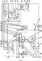
- Fig. 1 and 2 show circuit diagrams of devices for obtaining DC voltage
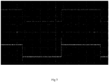
- fig. 3 and 4 show timing diagrams of the voltages on the load, taken from the description of US patent no. 6747420B2 (prototype) and obtained as a result of experimentation with the second embodiment of the device for obtaining DC voltage according to the invention.
- the device for obtaining DC voltage comprises:
- the proposed device for obtaining DC voltage operates as follows.
- the constant-frequency rectangular impulse generator (3) Upon the arrival of DC voltage from the outputs (5) and (7) of the DC voltage source (1) at the corresponding inputs (4) and (6) of the constant-frequency rectangular impulse generator (3) (inputs of the DC-pulse voltage converter (2)), the constant-frequency rectangular impulse generator (3) generates constant-frequency rectangular impulses, which pass from the output (13) of the constant-frequency rectangular impulse generator (3) to the 'information' input (12) of the controlled switch (11), and, if the contacts of the controlled switch (11) are closed, the constant-frequency rectangular impulses pass from its output (21) over the following path: First capacitor (19) - primary winding (outputs (23) and (24)) of the transformer (25) - secondary winding (outputs (28) and (29)) of the transformer (25) - second capacitor (26) and the parallel diode (31) and resistor (34) on the gate (39) and source (40) of the MOSFET (37).
- the MOSFET (37) converts the DC voltage passing from the output (5) of the DC voltage source (1) to the drain (38) of the MOSFET (37) into pulse voltage, and these pulses pass from the source (40) of the MOSFET (37) to the first input of the pulse voltage DC converter (41) (on the output (46) of the choke (45)), at the output of which (output (50) of the choke (45)), following appropriate conversion (diode (42)) and filtration (choke (45) and capacitor (47)), DC voltage begins to build.
- Part of this voltage which is defined by the position of the slider of the first (variable) resistor (86) passes from the output of the DC output voltage selector (85) (from the output (91) of the resistor (86)) to the inverting ("-") input (98) of the first operational amplifier (94) (the first input of the control circuit (93)), on the non-inverting ("+") input (95) of which voltage arrives from the positive output (96) of the first reference voltage source (97).
- a control voltage is formed that passes from the output (106) of the first operational amplifier (94) to the first input (105) of the combiner (105) of the control circuit (93).
- control voltage passes to the control input of the DC-pulse voltage converter (2) (to the non-inverting (110) input ("+") of the operational amplifier (14)).
- the control voltage that has arrived at the non-inverting (110) input (“+") of the operational amplifier (14) is compared with the voltage of the reference voltage source (8) that passes from its output (18) to the inverting ("-") input (17) of the operational amplifier (14).
- the voltage obtained as a result of the comparison passes from the output (15) of the operational amplifier (14) to the control input (16) of the controlled switch (11), which either closes or opens its contacts and thus changes the load factor of the pulses arriving at the gate (39) of the MOSFET (37) of the DC-pulse voltage converter (2) via the following path: First capacitor (19) - primary winding of the transformer (25) - secondary winding of the transformer (25) - second capacitor (26) and parallel diode (31) and resistor (34).
- the load factor of the constant-frequency rectangular impulses increases over the following path: First capacitor (19) - primary winding of the transformer (25) - secondary winding of the transformer (25) - second capacitor (26) and parallel diode (31) and resistor (34) - to the gate (39) of the MOSFET (37), as a result of which, after they pass from the source (40) of the MOSFET (37) to the input of the pulse voltage-DC converter (41) (output (46) of the choke (50)) and are transformed into DC voltage, the DC voltage on the load (51) decreases to the selected level.
- the DC voltage on the load (51) is stabilised (with small pulses) at the selected level, which is determined by the DC output voltage selector (85) and may be set in a wide range of up to hundreds of volts and more.
- Voltage from the output current selector of the proportional regulator (59) arrives at the non-inverting ("+") input (73) of the operational amplifier (72) of the proportional regulator (59) from the output (74) of the second (variable) resistor (64) of the proportional regulator (59).
- the DC current through the load (51) is stabilised (due to the effect of the negative feedback through the feedback node (82)) with small pulses at the level specified by the output current selector.
- the power at the collector (55)-emitter (57) junction of the controlled transistor (54) dissipates in proportion to the current through the controlled transistor (54) and the voltage drop at the junction.
- the voltage from the collector (55) of the controlled transistor (54) passes to the inverting ("-") input (103) of the second operational amplifier (99) of the control circuit (93), at the non-inverting ("+") input (100) of which voltage arrives from the second reference voltage source (102) of the control circuit (93).
- a control voltage is formed that passes to the second input (107) of the combiner (104) of the control circuit (93).
- the control voltage passes to the control input of the DC-pulse voltage converter (2) (to the non-inverting (110) input ("+") of the operational amplifier (14)).
- the control voltage that has arrived at the non-inverting (110) input (“+") of the operational amplifier (14) is compared with the voltage of the DC voltage source (8) that passes from its output (18) to the inverting ("-") input (17) of the operational amplifier (14).
- the voltage obtained as a result of the comparison passes from the output (15) of the operational amplifier (14) to the control input (16) of the controlled switch (11), which either closes or opens its contacts and thus changes the load factor of the pulses arriving at the gate (39) of the MOSFET (37) of the DC-pulse voltage converter (2).
- the load factor of the constant-frequency rectangular impulses increases over the following path: First capacitor (19) - primary winding of the transformer (25) - secondary winding of the transformer (25) - second capacitor (26) and parallel diode (31) and resistor (34) - to the gate (39) of the MOSFET (37), as a result of which, after they pass from the source (40) of the MOSFET (37) to the input of the pulse voltage-DC converter (41) (output (46) of the choke (45)) and are transformed into DC voltage, the voltage drop at the collector (55)-emitter (57) junction of the controlled transistor (54) of the regulator (53) decreases to the selected level, which is the lowest possible level at which the functionality of the controlled transistor (54) can be guaranteed. Meanwhile, the power that dissipated at the collector (55)-emitter (57) junction of the controlled transistor (54) is the lowest possible power at the selected load current.
- the DC voltage at the collector (55) - emitter (57) junction of the controlled transistor (54) is stabilised at a level that is the lowest possible at which the functionality of the controlled transistor (54) can be guaranteed and is determined by the voltage of the second reference voltage source (102), which is part of the control circuit (93), thus ensuring dissipation power at the collector (55)- emitter (57) junction of the controlled transistor (54), i.e., minimal energy loss.
- the proposed device for obtaining DC voltage by including negative feedback between the regulator and the proportional regulator, ensures stabile DC voltage on the load over a wider range of output voltages, whilst substantially reducing the magnitude of the pulsed component of the output voltage and output current with minimal energy loss.
- the proposed device for obtaining DC voltage comprises:
- the proposed device for obtaining DC voltage operates as follows.
- the constant-frequency rectangular impulse generator (3) When DC voltage from the outputs (5) and (7) of the DC voltage source (1) arrives at the corresponding inputs (4) and (6) of the constant-frequency rectangular impulse generator (3) (inputs of the DC-pulse voltage converter (2)), the constant-frequency rectangular impulse generator (3) generates constant-frequency rectangular impulses that pass from the output (13) of the constant-frequency rectangular impulse generator (3) to the 'information' input (12) of the controlled switch (11), and, if the contacts of the controlled switch (11) are closed, the constant-frequency rectangular impulses pass from its output (21) to the gate (20) of the MOSFET (19), and, from its drain (26), to the output (25) of the primary winding of the transformer (24) of the first galvanic isolation node.
- Part of this voltage which is defined by the position of the slider of the first (variable) resistor (48) passes from the output of the DC output voltage selector (47) (from the output (50) of the resistor (48)) to the inverting ("-") input (86) of the first operational amplifier (82) (the first input of the control circuit (81)), on the non-inverting ("+") input (83) of which voltage arrives from the positive output (84) of the first reference voltage source (85).
- a control voltage is formed that passes from the output (94) of the first operational amplifier (82) to the first input (93) of the combiner (92) of the control circuit (81).
- control voltage passes via the second galvanic isolation node (98) to the control input of the DC-pulse voltage converter (2) (to the non-inverting (106) input ("+") of the operational amplifier (14)).
- the control voltage that has arrived at the inverting (106) input (“-") of the operational amplifier (14) is compared with the voltage of the reference voltage source (8) that passes from its output (18) to the non-inverting ("+") input (17) of the operational amplifier (14).
- the voltage obtained as a result of the comparison passes from the output (15) of the operational amplifier (14) to the control input (16) of the controlled switch (11), which either closes or opens its contacts and thus changes the load factor of the pulses arriving at the gate (20) of the MOSFET (19) of the DC-pulse voltage converter (2).
- the DC voltage on the load (37) is stabilised (with small pulses) at the selected level, which is determined by the DC output voltage selector (47) and may be set in a wide range of up to hundreds of volts and more.
- Voltage from the output current selector of the proportional regulator (55) arrives at the non-inverting ("+") input (69) of the operational amplifier (68) of the proportional regulator (55) from the output (70) of the second (variable) resistor (60) of the proportional regulator (55).
- the DC current through the load (37) is stabilised (due to the effect of the negative feedback through the feedback node (78)) with small pulses at the level specified by the output current selector.
- the power at the collector (41)-emitter (45) junction of the controlled transistor (40) dissipates in proportion to the current through the controlled transistor (40) and the voltage drop at the junction.
- the voltage from the collector (41) of the controlled transistor (40) passes to the inverting ("-") input (91) of the second operational amplifier (87) (second input of the control circuit (81)), at the non-inverting ("+") input (88) of which voltage arrives from the positive output (89) of the second reference voltage source (90).
- the control voltage passes via the second galvanic isolation node (98) to the control input of the DC-pulse voltage converter (2) (to the inverting (106) input ("-") of the operational amplifier (14)).
- the control voltage that has arrived at the inverting (106) input (“-") of the operational amplifier (14) is compared with the voltage of the DC voltage source (8) that passes from its output (18) to the non-inverting ("+") input (17) of the operational amplifier (14).
- the voltage obtained as a result of the comparison passes from the output (15) of the operational amplifier (14) to the control input (16) of the controlled switch (11), which either closes or opens its contacts and thus changes the load factor of the pulses arriving at the gate (20) of the MOSFET (19) of the DC-pulse voltage converter (2).
- the power that dissipated at the collector (41)-emitter (45) junction of the controlled transistor (40) is the lowest possible power at the selected load current.
- the DC voltage at the collector (41) - emitter (45) junction of the controlled transistor (40) is stabilised at a level that is the lowest possible at which the functionality of the controlled transistor (40) can be guaranteed and is determined by the voltage of the second reference voltage source (90), which is part of the control circuit (81), thus ensuring dissipation power at the collector (41)- emitter (45) junction of the controlled transistor (40), i.e., minimal energy loss.
- the proposed device for obtaining DC voltage by including negative feedback between the regulator and the proportional regulator, ensures stabile DC voltage on the load over a wider range of output voltages, whilst substantially reducing the magnitude of the pulsed component of the output voltage and output current with minimal energy loss.
- a timing diagram of voltage on a load taken from the description of US patent no. 6747420B2 is shown in fig. 4 .
- a comparison of the timing diagrams shows that the stability of the DC voltage on the load is substantially increased compared to the solution shown in US patent no. 6747420B2 , and the pulsed component is reduced practically to nil.
- the function blocks of the device may be provided in various ways.
- the transistor of the regulator may be either bipolar, a MOSFET, or an IGBT;
- the DC-pulse voltage converter may be provided in the form of a pulse-width modulator microcircuit, etc.
- the output voltage may be controlled by varying the corresponding reference voltage of the control circuit, e.g., using a pulse-width modulation-control voltage converter, or by converting the code of the control protocol (e.g., DALI) to control voltage, or any other conversion of control effect to control voltage.
- a pulse-width modulation-control voltage converter e.g., a pulse-width modulation-control voltage converter
- stable DC voltage will be obtained on the load over a wider range of output voltages with a substantial reduction of the pulsed component of the output voltage and output current, i.e., the aforementioned technical result will be obtained.
Landscapes
- Engineering & Computer Science (AREA)
- Power Engineering (AREA)
- Physics & Mathematics (AREA)
- Electromagnetism (AREA)
- General Physics & Mathematics (AREA)
- Radar, Positioning & Navigation (AREA)
- Automation & Control Theory (AREA)
- Dc-Dc Converters (AREA)
Applications Claiming Priority (1)
| Application Number | Priority Date | Filing Date | Title |
|---|---|---|---|
| PCT/RU2015/000571 WO2017043994A1 (fr) | 2015-09-09 | 2015-09-09 | Dispositif pour générer de la tension électrique continue (et variantes) |
Publications (2)
| Publication Number | Publication Date |
|---|---|
| EP3349090A1 true EP3349090A1 (fr) | 2018-07-18 |
| EP3349090A4 EP3349090A4 (fr) | 2019-06-12 |
Family
ID=58240283
Family Applications (1)
| Application Number | Title | Priority Date | Filing Date |
|---|---|---|---|
| EP15903691.2A Ceased EP3349090A4 (fr) | 2015-09-09 | 2015-09-09 | Dispositif pour générer de la tension électrique continue (et variantes) |
Country Status (6)
| Country | Link |
|---|---|
| US (2) | US10320302B2 (fr) |
| EP (1) | EP3349090A4 (fr) |
| JP (1) | JP6539410B2 (fr) |
| CN (1) | CN108139764B (fr) |
| RU (1) | RU2688659C1 (fr) |
| WO (1) | WO2017043994A1 (fr) |
Families Citing this family (1)
| Publication number | Priority date | Publication date | Assignee | Title |
|---|---|---|---|---|
| WO2018132028A1 (fr) * | 2017-01-10 | 2018-07-19 | Закрытое Акционерно Общество "Драйв" | Procédé de transformation de tension électrique continue en tension pulsée |
Family Cites Families (34)
| Publication number | Priority date | Publication date | Assignee | Title |
|---|---|---|---|---|
| US4063307A (en) * | 1976-06-28 | 1977-12-13 | Teletype Corporation | Direct current power converter with start-up and protection circuits |
| US4124884A (en) * | 1977-03-07 | 1978-11-07 | Bell Telephone Laboratories, Incorporated | DC to DC converter with regulated input impedance |
| DE3109612A1 (de) * | 1981-03-13 | 1982-09-23 | Robert Bosch Gmbh, 7000 Stuttgart | Spannungswandler |
| US4400767A (en) * | 1981-06-30 | 1983-08-23 | Honeywell Information Systems Inc. | Self start flyback power supply |
| US4383293A (en) * | 1981-11-16 | 1983-05-10 | Acme Electric Corporation | Isolated DC current sense circuit |
| SU1229742A1 (ru) | 1984-09-28 | 1986-05-07 | Предприятие П/Я М-5178 | Стабилизатор напр жени с непрерывно-импульсным регулированием |
| SU1742807A1 (ru) * | 1990-10-15 | 1992-06-23 | Научно-исследовательский институт электротехники | Ключевой стабилизатор посто нного напр жени |
| GB9206022D0 (en) * | 1992-03-19 | 1992-04-29 | Astec Int Ltd | Push-pull inverter |
| DE19756233A1 (de) * | 1997-12-17 | 1999-07-01 | Siemens Ag | Strom-Spannungs-Regler |
| DE19942794A1 (de) * | 1999-09-08 | 2001-03-15 | Philips Corp Intellectual Pty | Konverter mit Hochsetzstelleranordnung |
| KR100419393B1 (ko) * | 1999-12-09 | 2004-02-21 | 산켄덴키 가부시키가이샤 | Dc-dc 컨버터 |
| DE20023993U1 (de) * | 2000-03-17 | 2008-09-25 | Tridonicatco Gmbh & Co. Kg | Ansteuerschaltung für Leuchtdioden |
| US6313616B1 (en) * | 2000-09-21 | 2001-11-06 | Home Touch Lighting Systems Llc | Switching buck converter with floating regulator |
| JP3391384B2 (ja) * | 2000-12-04 | 2003-03-31 | サンケン電気株式会社 | Dc−dcコンバータ |
| JP3371962B2 (ja) * | 2000-12-04 | 2003-01-27 | サンケン電気株式会社 | Dc−dcコンバ−タ |
| JP3494223B2 (ja) * | 2001-12-03 | 2004-02-09 | サンケン電気株式会社 | Dc−dcコンバ−タ |
| JP4096201B2 (ja) * | 2002-09-04 | 2008-06-04 | サンケン電気株式会社 | Dc−dc変換器 |
| US6944034B1 (en) * | 2003-06-30 | 2005-09-13 | Iwatt Inc. | System and method for input current shaping in a power converter |
| JP4210850B2 (ja) * | 2004-03-12 | 2009-01-21 | サンケン電気株式会社 | スイッチング電源装置 |
| JP4251128B2 (ja) * | 2004-09-30 | 2009-04-08 | ヤマハ株式会社 | スイッチング電源装置 |
| RU2303281C1 (ru) | 2006-01-10 | 2007-07-20 | Государственное образовательное учреждение высшего профессионального образования "Сибирский государственный аэрокосмический университет имени академика М.Ф. Решетнева" (СибГАУ) | Вторичный источник питания |
| JP5032893B2 (ja) * | 2007-06-07 | 2012-09-26 | 新日本無線株式会社 | 昇圧回路 |
| JP4210868B2 (ja) * | 2007-06-15 | 2009-01-21 | サンケン電気株式会社 | スイッチング電源装置 |
| US20110163693A1 (en) * | 2008-07-07 | 2011-07-07 | Osram Gesellschaft Mit Beschraenkter Haftung | Circuit arrangement and method for operating at least one led |
| US8792257B2 (en) * | 2011-03-25 | 2014-07-29 | Power Systems Technologies, Ltd. | Power converter with reduced power dissipation |
| EP2571152A1 (fr) * | 2011-09-17 | 2013-03-20 | Braun GmbH | Convertisseur CC avec tension de sortie ajustable |
| RU2510764C2 (ru) * | 2012-08-07 | 2014-04-10 | Закрытое Акционерное Общество "Драйв" | Устройство для получения постоянного тока, протекающего в цепи питания нагрузки |
| US9595875B2 (en) * | 2013-07-29 | 2017-03-14 | Texas Instruments Incorporated | Voltage converter compensation apparatus and methods |
| US9239584B2 (en) * | 2013-11-19 | 2016-01-19 | Tower Semiconductor Ltd. | Self-adjustable current source control circuit for linear regulators |
| US10444775B2 (en) * | 2014-05-12 | 2019-10-15 | Drive Cjsc | Apparatus for producing unvarying direct load current |
| US10038374B2 (en) * | 2014-08-26 | 2018-07-31 | Drive Cjsc | Apparatus for producing unvarying direct load current |
| CA2956281C (fr) * | 2014-08-26 | 2018-02-27 | Closed-Up Joint-Stock Company Drive | Dispositif de production de courant continu pour l'alimentation d'une charge |
| EP3327536B1 (fr) * | 2015-07-17 | 2022-02-23 | Closed-up Joint-Stock Company Drive | Régulateur de courant continu circulant dans un circuit d'alimentation de charge |
| US10122287B2 (en) * | 2016-02-24 | 2018-11-06 | Infineon Technologies Austria Ag | Power supply systems and feedback through a transformer |
-
2015
- 2015-09-09 EP EP15903691.2A patent/EP3349090A4/fr not_active Ceased
- 2015-09-09 JP JP2018512200A patent/JP6539410B2/ja not_active Expired - Fee Related
- 2015-09-09 RU RU2018108216A patent/RU2688659C1/ru active
- 2015-09-09 WO PCT/RU2015/000571 patent/WO2017043994A1/fr not_active Ceased
- 2015-09-09 US US15/757,180 patent/US10320302B2/en active Active
- 2015-09-09 CN CN201580083026.XA patent/CN108139764B/zh not_active Expired - Fee Related
-
2019
- 2019-03-06 US US16/293,873 patent/US10727752B2/en not_active Expired - Fee Related
Also Published As
| Publication number | Publication date |
|---|---|
| US20180278166A1 (en) | 2018-09-27 |
| US10320302B2 (en) | 2019-06-11 |
| RU2688659C1 (ru) | 2019-05-22 |
| EP3349090A4 (fr) | 2019-06-12 |
| JP2018526963A (ja) | 2018-09-13 |
| US10727752B2 (en) | 2020-07-28 |
| CN108139764B (zh) | 2020-09-08 |
| WO2017043994A1 (fr) | 2017-03-16 |
| CN108139764A (zh) | 2018-06-08 |
| US20190267904A1 (en) | 2019-08-29 |
| JP6539410B2 (ja) | 2019-07-03 |
Similar Documents
| Publication | Publication Date | Title |
|---|---|---|
| US10211741B2 (en) | Systems and methods for voltage regulation of primary side regulated power conversion systems with compensation mechanisms | |
| KR101214172B1 (ko) | 동기 정류 회로 및 이를 이용한 다중 출력을 갖는 전원공급장치 | |
| CN109039027A (zh) | 用于共源共栅电流感测的多级栅极驱动 | |
| RU2672669C2 (ru) | Устройство для получения постоянного тока, протекающего в цепи питания нагрузки (варианты) | |
| US10727752B2 (en) | Device for producing constant voltage (variants) | |
| CN106605182B (zh) | 用于产生流入负载的电源电路的直流电流的装置 | |
| TWI674742B (zh) | 直流電壓-脈衝電壓轉換器 | |
| RU2658681C1 (ru) | Устройство для преобразования постоянного напряжения в импульсное напряжение | |
| CN106464243B (zh) | 电子开关 | |
| KR102054359B1 (ko) | 직류전압 - 펄스전압 변환방법 | |
| TWI682615B (zh) | 直流電壓-脈衝電壓轉換裝置 | |
| RU2661348C1 (ru) | Устройство для преобразования постоянного напряжения в импульсное напряжение | |
| RU2666786C2 (ru) | Способ преобразования постоянного напряжения в импульсное напряжение | |
| HK1254877B (zh) | Dc电压-脉冲电压转换的方法 | |
| HK1239852B (en) | Device for producing direct load current |
Legal Events
| Date | Code | Title | Description |
|---|---|---|---|
| STAA | Information on the status of an ep patent application or granted ep patent |
Free format text: STATUS: THE INTERNATIONAL PUBLICATION HAS BEEN MADE |
|
| PUAI | Public reference made under article 153(3) epc to a published international application that has entered the european phase |
Free format text: ORIGINAL CODE: 0009012 |
|
| STAA | Information on the status of an ep patent application or granted ep patent |
Free format text: STATUS: REQUEST FOR EXAMINATION WAS MADE |
|
| 17P | Request for examination filed |
Effective date: 20180306 |
|
| AK | Designated contracting states |
Kind code of ref document: A1 Designated state(s): AL AT BE BG CH CY CZ DE DK EE ES FI FR GB GR HR HU IE IS IT LI LT LU LV MC MK MT NL NO PL PT RO RS SE SI SK SM TR |
|
| AX | Request for extension of the european patent |
Extension state: BA ME |
|
| DAV | Request for validation of the european patent (deleted) | ||
| DAX | Request for extension of the european patent (deleted) | ||
| A4 | Supplementary search report drawn up and despatched |
Effective date: 20190513 |
|
| RIC1 | Information provided on ipc code assigned before grant |
Ipc: G05F 1/59 20060101AFI20190507BHEP Ipc: H02M 3/335 20060101ALI20190507BHEP Ipc: H02M 3/158 20060101ALI20190507BHEP Ipc: H02M 1/15 20060101ALI20190507BHEP |
|
| STAA | Information on the status of an ep patent application or granted ep patent |
Free format text: STATUS: EXAMINATION IS IN PROGRESS |
|
| 17Q | First examination report despatched |
Effective date: 20200225 |
|
| REG | Reference to a national code |
Ref country code: DE Ref legal event code: R003 |
|
| STAA | Information on the status of an ep patent application or granted ep patent |
Free format text: STATUS: THE APPLICATION HAS BEEN REFUSED |
|
| 18R | Application refused |
Effective date: 20230118 |