EP3349267B1 - Appareil d'éclairage faisant appel à un dispositif électroluminescent organique et son procédé de fabrication - Google Patents
Appareil d'éclairage faisant appel à un dispositif électroluminescent organique et son procédé de fabrication Download PDFInfo
- Publication number
- EP3349267B1 EP3349267B1 EP17210695.7A EP17210695A EP3349267B1 EP 3349267 B1 EP3349267 B1 EP 3349267B1 EP 17210695 A EP17210695 A EP 17210695A EP 3349267 B1 EP3349267 B1 EP 3349267B1
- Authority
- EP
- European Patent Office
- Prior art keywords
- light emitting
- electrode
- organic light
- emitting layer
- pad
- Prior art date
- Legal status (The legal status is an assumption and is not a legal conclusion. Google has not performed a legal analysis and makes no representation as to the accuracy of the status listed.)
- Active
Links
Images






Classifications
-
- H—ELECTRICITY
- H10—SEMICONDUCTOR DEVICES; ELECTRIC SOLID-STATE DEVICES NOT OTHERWISE PROVIDED FOR
- H10K—ORGANIC ELECTRIC SOLID-STATE DEVICES
- H10K50/00—Organic light-emitting devices
- H10K50/80—Constructional details
- H10K50/88—Terminals, e.g. bond pads
-
- H—ELECTRICITY
- H10—SEMICONDUCTOR DEVICES; ELECTRIC SOLID-STATE DEVICES NOT OTHERWISE PROVIDED FOR
- H10K—ORGANIC ELECTRIC SOLID-STATE DEVICES
- H10K50/00—Organic light-emitting devices
- H10K50/80—Constructional details
- H10K50/805—Electrodes
- H10K50/82—Cathodes
- H10K50/822—Cathodes characterised by their shape
-
- H—ELECTRICITY
- H05—ELECTRIC TECHNIQUES NOT OTHERWISE PROVIDED FOR
- H05B—ELECTRIC HEATING; ELECTRIC LIGHT SOURCES NOT OTHERWISE PROVIDED FOR; CIRCUIT ARRANGEMENTS FOR ELECTRIC LIGHT SOURCES, IN GENERAL
- H05B33/00—Electroluminescent light sources
- H05B33/10—Apparatus or processes specially adapted to the manufacture of electroluminescent light sources
-
- H—ELECTRICITY
- H05—ELECTRIC TECHNIQUES NOT OTHERWISE PROVIDED FOR
- H05B—ELECTRIC HEATING; ELECTRIC LIGHT SOURCES NOT OTHERWISE PROVIDED FOR; CIRCUIT ARRANGEMENTS FOR ELECTRIC LIGHT SOURCES, IN GENERAL
- H05B33/00—Electroluminescent light sources
- H05B33/12—Light sources with substantially two-dimensional [2D] radiating surfaces
-
- H—ELECTRICITY
- H10—SEMICONDUCTOR DEVICES; ELECTRIC SOLID-STATE DEVICES NOT OTHERWISE PROVIDED FOR
- H10K—ORGANIC ELECTRIC SOLID-STATE DEVICES
- H10K50/00—Organic light-emitting devices
- H10K50/10—OLEDs or polymer light-emitting diodes [PLED]
- H10K50/11—OLEDs or polymer light-emitting diodes [PLED] characterised by the electroluminescent [EL] layers
-
- H—ELECTRICITY
- H10—SEMICONDUCTOR DEVICES; ELECTRIC SOLID-STATE DEVICES NOT OTHERWISE PROVIDED FOR
- H10K—ORGANIC ELECTRIC SOLID-STATE DEVICES
- H10K50/00—Organic light-emitting devices
- H10K50/80—Constructional details
- H10K50/805—Electrodes
-
- H—ELECTRICITY
- H10—SEMICONDUCTOR DEVICES; ELECTRIC SOLID-STATE DEVICES NOT OTHERWISE PROVIDED FOR
- H10K—ORGANIC ELECTRIC SOLID-STATE DEVICES
- H10K50/00—Organic light-emitting devices
- H10K50/80—Constructional details
- H10K50/805—Electrodes
- H10K50/81—Anodes
- H10K50/814—Anodes combined with auxiliary electrodes, e.g. ITO layer combined with metal lines
-
- H—ELECTRICITY
- H10—SEMICONDUCTOR DEVICES; ELECTRIC SOLID-STATE DEVICES NOT OTHERWISE PROVIDED FOR
- H10K—ORGANIC ELECTRIC SOLID-STATE DEVICES
- H10K50/00—Organic light-emitting devices
- H10K50/80—Constructional details
- H10K50/805—Electrodes
- H10K50/82—Cathodes
-
- H—ELECTRICITY
- H10—SEMICONDUCTOR DEVICES; ELECTRIC SOLID-STATE DEVICES NOT OTHERWISE PROVIDED FOR
- H10K—ORGANIC ELECTRIC SOLID-STATE DEVICES
- H10K50/00—Organic light-emitting devices
- H10K50/80—Constructional details
- H10K50/84—Passivation; Containers; Encapsulations
- H10K50/841—Self-supporting sealing arrangements
-
- H—ELECTRICITY
- H10—SEMICONDUCTOR DEVICES; ELECTRIC SOLID-STATE DEVICES NOT OTHERWISE PROVIDED FOR
- H10K—ORGANIC ELECTRIC SOLID-STATE DEVICES
- H10K50/00—Organic light-emitting devices
- H10K50/80—Constructional details
- H10K50/84—Passivation; Containers; Encapsulations
- H10K50/842—Containers
- H10K50/8426—Peripheral sealing arrangements, e.g. adhesives, sealants
-
- H—ELECTRICITY
- H10—SEMICONDUCTOR DEVICES; ELECTRIC SOLID-STATE DEVICES NOT OTHERWISE PROVIDED FOR
- H10K—ORGANIC ELECTRIC SOLID-STATE DEVICES
- H10K59/00—Integrated devices, or assemblies of multiple devices, comprising at least one organic light-emitting element covered by group H10K50/00
- H10K59/10—OLED displays
- H10K59/17—Passive-matrix OLED displays
- H10K59/179—Interconnections, e.g. wiring lines or terminals
-
- H—ELECTRICITY
- H10—SEMICONDUCTOR DEVICES; ELECTRIC SOLID-STATE DEVICES NOT OTHERWISE PROVIDED FOR
- H10K—ORGANIC ELECTRIC SOLID-STATE DEVICES
- H10K59/00—Integrated devices, or assemblies of multiple devices, comprising at least one organic light-emitting element covered by group H10K50/00
- H10K59/80—Constructional details
- H10K59/805—Electrodes
-
- H—ELECTRICITY
- H10—SEMICONDUCTOR DEVICES; ELECTRIC SOLID-STATE DEVICES NOT OTHERWISE PROVIDED FOR
- H10K—ORGANIC ELECTRIC SOLID-STATE DEVICES
- H10K71/00—Manufacture or treatment specially adapted for the organic devices covered by this subclass
-
- H—ELECTRICITY
- H10—SEMICONDUCTOR DEVICES; ELECTRIC SOLID-STATE DEVICES NOT OTHERWISE PROVIDED FOR
- H10K—ORGANIC ELECTRIC SOLID-STATE DEVICES
- H10K77/00—Constructional details of devices covered by this subclass and not covered by groups H10K10/80, H10K30/80, H10K50/80 or H10K59/80
- H10K77/10—Substrates, e.g. flexible substrates
- H10K77/111—Flexible substrates
-
- F—MECHANICAL ENGINEERING; LIGHTING; HEATING; WEAPONS; BLASTING
- F21—LIGHTING
- F21Y—INDEXING SCHEME ASSOCIATED WITH SUBCLASSES F21K, F21L, F21S and F21V, RELATING TO THE FORM OR THE KIND OF THE LIGHT SOURCES OR OF THE COLOUR OF THE LIGHT EMITTED
- F21Y2115/00—Light-generating elements of semiconductor light sources
- F21Y2115/10—Light-emitting diodes [LED]
- F21Y2115/15—Organic light-emitting diodes [OLED]
-
- H—ELECTRICITY
- H10—SEMICONDUCTOR DEVICES; ELECTRIC SOLID-STATE DEVICES NOT OTHERWISE PROVIDED FOR
- H10K—ORGANIC ELECTRIC SOLID-STATE DEVICES
- H10K2102/00—Constructional details relating to the organic devices covered by this subclass
- H10K2102/301—Details of OLEDs
- H10K2102/311—Flexible OLED
-
- H—ELECTRICITY
- H10—SEMICONDUCTOR DEVICES; ELECTRIC SOLID-STATE DEVICES NOT OTHERWISE PROVIDED FOR
- H10K—ORGANIC ELECTRIC SOLID-STATE DEVICES
- H10K71/00—Manufacture or treatment specially adapted for the organic devices covered by this subclass
- H10K71/851—Division of substrate
-
- Y—GENERAL TAGGING OF NEW TECHNOLOGICAL DEVELOPMENTS; GENERAL TAGGING OF CROSS-SECTIONAL TECHNOLOGIES SPANNING OVER SEVERAL SECTIONS OF THE IPC; TECHNICAL SUBJECTS COVERED BY FORMER USPC CROSS-REFERENCE ART COLLECTIONS [XRACs] AND DIGESTS
- Y02—TECHNOLOGIES OR APPLICATIONS FOR MITIGATION OR ADAPTATION AGAINST CLIMATE CHANGE
- Y02E—REDUCTION OF GREENHOUSE GAS [GHG] EMISSIONS, RELATED TO ENERGY GENERATION, TRANSMISSION OR DISTRIBUTION
- Y02E10/00—Energy generation through renewable energy sources
- Y02E10/50—Photovoltaic [PV] energy
- Y02E10/549—Organic PV cells
Definitions
- the present disclosure relates to a lighting apparatus using an organic light emitting device with a simplified fabrication process, and a fabrication method thereof.
- the incandescent lamp has a good color rendering index but has a low energy efficiency
- the fluorescent lamp has a good efficiency, but has a low color rendering index and contains mercury and thus has an environmental problem.
- the light emitting diode is composed of an inorganic light emitting material, and has the highest luminous efficiency in a blue wavelength band, but has a lower luminous efficiency as it goes toward a red and a green wavelength band, which is a color having the highest visual sensitivity. Therefore, there is a problem in that the luminous efficiency is reduced when white light with a combination of a red light emitting diode, a green light emitting diode, and a blue light emitting diode is emitted. Furthermore, since the width of each emission peak is narrow when a red light emitting diode, a green light emitting diode, and a blue light emitting diode are used, there is also a problem in that the color rendering property deteriorates.
- a lighting apparatus for combining a blue light emitting diode with a yellow colored phosphor instead of combining a red light emitting diode, a green light emitting diode and a blue light emitting diode to output white light has been proposed.
- the reason why the light emitting diode having such a structure is proposed is that a method of using only a blue light emitting diode having a higher luminous efficiency and using a fluorescent material that receives blue light to emit yellow light for the remaining colors is more efficient than that of using a green light emitting diode having a low luminous efficiency.
- the fluorescent material itself that emits yellow light has a poor luminous efficiency, and thus there is a limit in enhancing the luminous efficiency of the lighting apparatus.
- EP 2849534 A1 presents an organic EL device that can efficiently equalize heat generated in an organic EL element during use while preventing moisture from invading in the organic EL element.
- the light emitting element is covered with an inorganic sealing layer, an adhesive layer, an insulating resin film, and a metallic foil in this order.
- the organic EL device includes a current carrying area that is located outside an emission area and provided along a part of an edge of the emission area. A heat-conductive sealing stacked layer structure is formed in the current carrying area.
- a first electrode layer extended from the emission area auxiliary electrode layers having heat conductivity larger than that of the first electrode layer, the inorganic sealing layer, the adhesive layer, and a heat-conductive sealing layer are in direct contact with each other in this order in the heat-conductive sealing stacked layer structure.
- the heat-conductive sealing stacked layer structure having a linear shape is located near at least one side of a transparent substrate.
- JP 2014/192050 and JP 2012/181931 disclose OLED lamps with electrode contacts that are made by forming trenches in the uniformly deposited organic and second electrode layers.
- the present disclosure is contrived to solve the aforementioned problem and an object of the present disclosure is to provide a lighting apparatus that can be fabricated by entirely depositing an organic light emitting layer on a substrate without using a mask, and a fabrication method thereof.
- Another object of the present disclosure is to provide a lighting apparatus for depositing an organic light emitting material and a metal on a film being transported between rolls in a state that a region formed with a pad is blocked by a roll fabrication apparatus having a shielding member to allow a continuous and rapid process, and a fabrication method thereof.
- a lighting apparatus may be fabricated on a film being transported in a roll fabrication apparatus, thereby allowing a continuous and rapid fabrication of a lighting apparatus.
- the deposition of an organic light emitting material and a metal may be carried out without using an additional mask, thereby facilitating facilities and simplifying fabrication processes.
- an organic light emitting material and a metal layer may be deposited in a state that an edge region of a film being transported is blocked by a shielding member not to form an organic light emitting layer and a second electrode in a region formed with a pad, thereby opening the pad.
- a lighting apparatus may be completed by separating a film as it is cut in a width direction, and at this time, the organic light emitting layer and the second electrode may be exposed to the outside through the cut surface.
- An open region from which the organic light emitting layer and the second electrode are removed in parallel to both cut surfaces may be formed within the lighting apparatus spaced apart from the cut surface of the film (i.e., substrate). Accordingly, the organic light emitting layer exposed to the outside may be disconnected from the open region, thereby preventing moisture and air infiltrated through the organic light emitting layer from being propagated through the organic light emitting layer into the lighting apparatus through the organic light emitting layer.
- a first electrode, an organic light emitting layer, and a second electrode are formed on a lighting portion of the lighting apparatus to form an organic light emitting device, and a first pad is connected to the first electrode and a second pad is connected to the second electrode to apply a voltage thereto.
- a portion of the organic light emitting layer is laser-etched to form a contact portion, and the second electrode is electrically connected to the second pad through the contact portion.
- a lighting apparatus is provided as defined in claim 1.
- the second pad is electrically connected to the second electrode through a contact portion formed on the same layer as that of the first pad and formed on the organic light emitting layer.
- the organic light emitting layer and the second electrode have the same area, and the organic light emitting layer is disposed between the second electrode and the second pad.
- the contact portion is a region in which the organic light emitting layer in a region where the organic light emitting layer overlap with the second electrode is removed by a laser.
- the contact portion is formed in a band shape.
- the contact portion is formed in a hole shape.
- the first pad and the second pad are disposed in an upper edge region or an upper and a lower side edge region of the first substrate.
- the first substrate is formed of a flexible film.
- the first substrate is formed of glass.
- the lighting apparatus may further comprise a second substrate adhered to the first substrate by an adhesive.
- the second substrate is formed of material selected from the group consisting of a polymer film, a metal foil and glass.
- the lighting apparatus may further comprise an auxiliary electrode disposed in the lighting portion and the first and second outer portions of the substrate, the auxiliary electrode being connected to the first electrode.
- the auxiliary electrode is disposed in a matrix shape, a mesh shape, an octagonal shape, a hexagonal shape, and a circular shape within the lighting portion with a preset width.
- a method of fabricating a lighting apparatus comprising: forming an auxiliary electrode, a first electrode, a first pad, and a second pad in a plurality of lighting apparatus regions arranged along a length direction of a first substrate; entirely depositing an organic light emitting material on the lighting apparatus regions to form an organic light emitting layer; entirely depositing a metal on the lighting apparatus regions to form a second electrode on the organic light emitting layer; removing the second electrode and the organic light emitting layer in an edge of the lighting apparatus regions along a width direction of the first substrate to form an open region; and adhering a second substrate onto the second electrode by an adhesive.
- the method may further comprise removing the organic light emitting layer to form a contact portion for electrically connecting the second electrode to the second pad.
- the forming the contact portion may comprise etching the organic light emitting layer by a laser.
- the forming the open region may comprise etching the second electrode and the organic light emitting layer by a laser.
- the organic light emitting material and the metal may be deposited by a roll fabrication apparatus.
- the roll fabrication apparatus may comprise a shielding member for blocking a first pad and a second pad formation region to deposit the organic light emitting material and the metal on a film excluding the first pad and the second pad formation region.
- the method may further comprise cutting the adhered first and second substrates to separate a plurality of lighting apparatus regions.
- the organic light emitting layer and the second electrode may be exposed to the outside through the cut lateral end surface.
- the process may be carried out on a film transported between rolls by a roll fabrication apparatus, thereby allowing a rapid and continuous fabrication process of a lighting apparatus.
- a lighting apparatus may be fabricated without using an additional mask, thereby reducing the cost of facilities and decreasing the installation space of facilities.
- an open region may be formed on an organic light emitting layer exposed through a lateral end surface to disconnect the organic light emitting layer, thereby preventing moisture or air from being infiltrated into the lighting apparatus through the organic light emitting layer.
- the present disclosure provides a lighting apparatus including an organic light emitting device made of an organic material rather than a lighting apparatus including an inorganic light emitting device made of an inorganic material.
- An organic light emitting device made of an organic light emitting material has a relatively good luminous efficiency in green and red colors as compared with an inorganic light emitting device.
- an organic light emitting device has a relatively larger width in blue, red and green emission peaks as compared with an inorganic light emitting device, and thus it has an advantage in that the color rendering property thereof is improved and the light of the light emitting apparatus is more similar to the sunlight.
- the lighting apparatus may be fabricated by a roll-to-roll process due to a roll fabrication apparatus, and the process may be continuously carried out, thereby allowing a rapid fabrication of the lighting apparatus.
- an organic light emitting layer which is a part of the organic light emitting device, and an electrode thereon may be formed without using an additional mask not to use an expensive mask, thereby reducing fabrication cost.
- FIG. 1 is a view illustrating the structure of a lighting apparatus using an organic light emitting diode according to the present disclosure.
- the lighting apparatus according to the present disclosure is a flexible lighting apparatus capable of being bent.
- the lighting apparatus 100 is a surface emitting lighting apparatus, which includes a lighting portion (EA) that emits actual light to output the light to the outside, and outer portions (NA1, NA2) at the outside thereof.
- a first electrode 124 and a second electrode 126 are disposed over an entire surface of the first substrate 110, and an organic light emitting layer 130 is formed between the first electrode 124 and the second electrode 126 to form an organic light emitting device.
- the lighting apparatus 100 having such a structure, as a signal is applied to the first electrode 124 and the second electrode 126 of the organic light emitting device, the organic light emitting layer 130 emits light over the entire substrate 110.
- a matrix-shaped auxiliary electrode 122 is disposed in a partial region of the lighting portion (EA) and the outer portions (NA1, NA2).
- the auxiliary electrode 122 is made of a metal having a high conductivity in such a manner that a uniform voltage is applied to the first electrode 124 of the entire lighting portion (EA) to allow emission having a uniform luminance over the large-area lighting apparatus 100.
- the organic light emitting layer 130 is formed of an organic light emitting material that outputs white light.
- the organic light emitting layer 130 may include a blue organic light emitting layer, a red organic light emitting layer and a green organic light emitting layer or may have a tandem structure including a blue light emitting layer and a yellow-green light emitting layer.
- the organic light emitting layer 130 of the present disclosure is not limited to the above structure, but various structures may be applied thereto.
- the present disclosure may include an electron injection layer and a hole injection layer for injecting electrons and holes respectively into the organic light emitting layer 130 of the present disclosure, an electron transport layer and a hole transport layer for transporting the injected electrons and holes respectively to the organic light emitting layer, and a charge generation layer that generates charges such as electrons and holes.
- a first pad 123a, a second pad 123b and a contact portion 129 for electrically connecting to the second pad 123b to the second electrode 126 are disposed at an upper side of the outer portion (NA1, NA2) of the first substrate 110.
- the first pad 123a and the second pad 123b are connected to an external signal source to apply a voltage to the first electrode and the second electrode.
- the first pad 123a is integrally formed with the first electrode 124, and the second pad 123b is formed of the same material as the first electrode 124 at the same layer, but the second pad 123b is separated from the first pad 123a and the first electrode 124 by a predetermined distance and electrically insulated therefrom.
- the organic light emitting layer 130 is not disposed on the upper and lower outer portions (NA1, NA2) in which the first pad 123a and the second pad 123b are disposed, but the organic light emitting layer 130 is disposed on the left and right outer portions (NA3, NA4) in which the first and second pads 123a and 123b are not disposed.
- NA1, NA2 the organic light emitting layer 130
- NA3, NA4 the organic light emitting layer 130 is not exposed on lateral end surfaces of the upper and lower sides of the lighting apparatus 100
- the organic light emitting layer 130 is exposed on lateral end surfaces of the left and right sides of the lighting apparatus 100.
- a plurality of the lighting apparatuses 100 are formed along a length direction of a film, and the film is cut subsequent to the completion of the process to separate the lighting apparatuses 10, respectively.
- a lateral end surface of the lighting apparatus 100 is a cut surface of the film.
- the organic light emitting layer 130 is deposited on the entire region along a length direction of the film, and thus the organic light emitting layer 130 is exposed to the outside through the cut surface, namely, a lateral end surface of the lighting apparatus 100, when the film is cut.
- the organic light emitting layer 130 As described above, as the organic light emitting layer 130 is exposed through lateral end surfaces of the left and right sides of the lighting apparatus 100, moisture or air infiltrated into the organic light emitting layer 130 may be infiltrated into the lighting portion (EA) along the organic light emitting layer 130.
- EA lighting portion
- the light emitting property is rapidly deteriorated to reduce a luminescent efficiency of the organic light emitting layer 130.
- moisture is propagated into the entire lighting apparatus 100 along the organic light emitting layer 130 to reduce a light emitting efficiency of the lighting apparatus 100.
- a part of the organic light emitting layer 130 is removed in the left and right outer portions (NA3, NA4) of the lighting apparatus 100 to form an open region 131 for disconnecting the organic light emitting layer 130, thereby preventing moisture from being propagated into the organic light emitting layer 130 of the lighting portion (EA) of the lighting apparatus 100 in which light is actually emitted.
- FIG. 2A is a cross-sectional view taken along line I-I' in FIG. 1 and FIG. 2A is a cross-sectional view taken along line II-II' in FIG. 1 , and the lighting apparatus 100 according to a first embodiment of the present disclosure will be described in more detail with reference thereto.
- the lighting apparatus of the present disclosure will be described as a flexible lighting apparatus having flexibility, but the present disclosure may be applicable not only to a flexible lighting apparatus of the present disclosure but also to a typical non-flexible lighting apparatus.
- the lighting apparatus 100 of the present embodiment may include a lighting portion (EA) that actually emits light, and outer portions (NA1, NA2, NA3, NA4) arranged along an outer circumference of the lighting portion (EA).
- EA lighting portion
- NA1, NA2, NA3, NA4 outer portions
- the first electrode 124 is disposed on the first substrate 110 made of a flexible soft transparent material such as plastic or a transparent material such as glass.
- a flexible material such as plastic
- the present disclosure is not limited to a structure formed of a soft material such as plastic, but may also be formed of a non-flexible material such as glass.
- the first substrate 110 is formed of glass as described above, it may be possible to fabricate the lighting apparatus 100 with a process of a general sheet method other than a process using a roll.
- the first electrode 124 is disposed on the lighting portion (EA) and the outer portions (NA1, NA2, NA3, NA4) and formed of a transparent conductive material having a good conductivity and a high work function.
- the first electrode 124 may be formed of indium tin oxide (ITO), indium zinc oxide (IZO), a tin oxide based and a zinc oxide based transparent conductive material or the like, and a transparent conductive polymer may also be used for the first electrode 124.
- first pad 123a and the second pad 123b are disposed on the first outer portion (NA1) and the second outer portion (NA2) of the first substrate 110, respectively.
- the first pad 123a and the second pad 123b are formed of the same material by the same process as the first electrode 124.
- the first electrode 124 is extended from the first pad 123a and thus the first pad 123a is formed integrally with the first electrode 124, but the second pad 123b is spaced apart from the first electrode 124 by a predetermined distance.
- the auxiliary electrode 122 is disposed on the lighting portion (EA) and the outer portions (NA1, NA2, NA3, NA4) of the first substrate 110, and electrically connected to the first electrode 124.
- the first electrode 124 has an advantage in that it is formed of a transparent conductive material to transmit light emitted therefrom, but also has a disadvantage in that an electrical resistance thereof is very higher than that of a metal. Accordingly, when the large-area lighting apparatus 100 is fabricated, the distribution of voltages applied to a wide lighting area becomes non-uniform due to a large resistance of the transparent conductive material, and such a non-uniform voltage distribution does not allow light emission having a uniform luminance on the large-area lighting apparatus 100.
- the auxiliary electrode 122 is disposed in a matrix shape with a small width, a mesh shape, a hexagonal shape, an octagonal shape, a circular shape, or the like over the entire lighting portion (EA) to uniformly apply a voltage to the first electrode 124 of the entire lighting apparatus 100, thereby allowing light emission having a uniform luminance on the large-area lighting apparatus 100.
- the auxiliary electrode 122 is disposed below the first electrode 124, but the auxiliary electrode 122 may also be disposed above the first electrode 124.
- the auxiliary electrode 122 is formed of a metal having a good conductivity such as Al, Au, Cu, Ti, W, Mo or an alloy thereof.
- the auxiliary electrode 122 may be formed with a double layer structure, but the auxiliary electrode 122 may also be formed with a single layer.
- a protective layer 112 is deposited on the lighting portion (EA) and the outer portions (NA1, NA2, NA3, NA4) of the first substrate 110.
- the protective layer 112 disposed on the lighting portion (EA) is configured to cover the auxiliary electrode 122 and the first electrode 124 thereon, and the protective layer 112 is not disposed on a light emitting area from which light is actually emitted.
- the protective layer 112 of the lighting portion (EA) is formed to surround the auxiliary electrode 122 so as to reduce a stepped portion due to the auxiliary electrode 122, and thus various layers to be formed thereafter will be stably formed without being disconnected.
- the protective layer 112 is formed of an inorganic layer such as SiOx or SiNx. However, the protective layer 112 may also be formed of an organic layer such as photoacryl or a plurality of layers having an inorganic layer and an organic layer.
- the organic light emitting layer 130 and the second electrode 126 are disposed in a partial region of the lighting portion (EA) and the outer portions (NA1, NA2, NA3, NA4).
- the organic light emitting layer 130 and the second electrode 126 are not formed in a partial region of the first and second outer portions (NA1, NA2) in which the first pad 123a and the second pad 123b are disposed, and thus the organic light emitting layer 130 and the second electrode 126 are not exposed to the outside through lateral end surfaces of two sides corresponding to this region of the lighting apparatus 100.
- the organic light emitting layer 130 and the second electrode 126 are formed in the third and fourth outer portions (NA3, NA4) in which the first pad 123a and the second pad 123b are not disposed, and thus exposed to the outside through lateral end surfaces of two sides corresponding to this region.
- an open region 131 from which the organic light emitting layer 130 and the second electrode 126 are removed with a preset width is formed in parallel to two sides of the lighting apparatus 100 formed in a region spaced apart from the two sides of the lighting apparatus 100 by a predetermined distance in the third and fourth outer portions (NA3, NA4) to disconnect the organic light emitting layer 130.
- the organic light emitting layer 130 may be formed of a red light emitting layer, a blue light emitting layer, and a green light emitting layer or configured with a tandem structure including a blue light emitting layer and a yellow-green light emitting layer as a white organic light emitting layer. Furthermore, the organic light emitting layer 130 may include an electron injection layer and a hole injection layer for injecting electrons and holes respectively into the organic light emitting layer, an electron transport layer and a hole transport layer for transporting the injected electrons and holes respectively to the organic light emitting layer, and a charge generation layer that generates charges such as electrons and holes.
- the second electrode 126 may be formed of a metal such as Ca, Ba, Mg, Al or Ag.
- the first electrode 124, the organic light emitting layer 130, and the second electrode 126 of the lighting portion (EA) form an organic light emitting device.
- the first electrode 124 is an anode of an organic light emitting device and the second electrode 126 is a cathode thereof, and a voltage is applied to the first electrode 124 and the second electrode 126, electrons are injected from the second electrode 126 into the organic light emitting layer 130 and holes are injected from the first electrode 124 into the organic light emitting layer 130 to generate excitons within the organic light emitting layer 130, and as excitons decay, light corresponding to an energy difference between LUMO (Lowest Unoccupied Molecular Orbital) and HOMO (Highest Occupied Molecular Orbital) of the light emitting layer is generated and emitted in a downward direction (toward the substrate 110 on the drawing).
- LUMO Local Unoccupied Molecular Orbital
- HOMO Highest Occupied Molecular Orbital
- the protective layer 112 is disposed on the auxiliary electrode 122 of the lighting portion (EA), and the organic light emitting layer 130 on the auxiliary electrode 122 is not directly in contact with the first electrode 124, and thus the organic light emitting device is not formed on the auxiliary electrode 122.
- the organic light emitting device within the lighting portion (EA) is formed only within the auxiliary electrode 122 in a matrix shape, for example.
- a partial region of the organic light emitting layer 130 on the second pad 123b of the second outer portion (NA2) is removed to form the contact portion 129, and thus the second electrode 126 is electrically connected to the second pad 123b through the contact portion 129.
- the contact portion 129 is an open region from which a partial region of the organic light emitting layer 130 is removed, namely, a contact hole.
- the contact portion 129 may be formed in various shapes, and in particular, according to the present disclosure, the organic light emitting layer 130 may be removed by a laser to form the contact portion 129.
- An adhesive 118 is coated on the first substrate 110 having the organic light emitting device and a second substrate 170 is disposed thereon, and the second substrate 170 is adhered by the adhesive 118 to seal the lighting apparatus 100.
- the adhesive 118 may be a photocurable adhesive or thermosetting adhesive.
- the second substrate 170 may be formed of various materials.
- the second substrate 170 is a substrate for preventing moisture or air from penetrating from the outside, and any material may be used as long as it can perform such a function.
- the second substrate 170 may be formed of a polymer such as PET (polyethyleneterephtalate) or may be formed of a thin metal foil such as aluminum.
- a non-flexible material such as glass may be used.
- the adhesive 118 applied to the first and second outer portions (NA1, NA2) in which the first pad 123a and the second pad 123b are disposed is also disposed on lateral end surfaces of the organic light emitting layer 130 and the second electrode 126 to seal the lateral end surfaces of the organic light emitting layer 130 and the second electrode 126.
- the adhesive 118 applied to the third and fourth outer portions (NA3, NA4) in which the first pad 123a and the second pad 123b are not disposed is extended and disposed up to a cross section of the lighting apparatus 100 of the organic light emitting layer 130 and the second electrode 126, and the adhesive 118 is disposed only on the second electrode 126.
- a protective layer formed of an organic layer and/or an inorganic layer and a sealant formed of an epoxy compound, an acrylate compound or an acrylic compound may be provided on the second electrode 126.
- a flexible circuit film such as an FPC (Flexible Printed Circuit) is adhered to the first pad 123a and the second pad 123b, respectively, and the first pad 123a and the second pad 123b are respectively connected to an external signal source to apply a signal to the first electrode 124 and the second electrode 126.
- FPC Flexible Printed Circuit
- the organic light emitting layer 130 and the second electrode 126 are sequentially deposited in the same region, and the second electrode 126 and the organic light emitting layer 130 insulated by interposing the organic light emitting layer 130 therebetween are electrically connected to each other through the contact portions 129 formed on the organic light emitting layer 130. Furthermore, according to the present disclosure, an open region 131 for disconnecting the organic light emitting layer 130 is formed in a predetermined region at two sides exposed through the lateral end surface of the organic light emitting layer 130 to prevent moisture or air from being propagated into the lighting portion (EA) through the organic light emitting layer 130 exposed at lateral end surfaces of the lighting apparatus 100.
- EA lighting portion
- FIG. 3 is a view schematically illustrating the structure of a roll fabrication apparatus 200 for fabricating a lighting apparatus according to the present disclosure.
- the roll fabrication apparatus 200 illustrated in FIG. 3 is an apparatus of performing an organic material deposition process for forming an organic light emitting layer and a metal deposition process for forming a second electrode during the fabrication process of the lighting apparatus 100 illustrated in FIG. 2 .
- the roll fabrication apparatus of the present disclosure may not be limited to only the process of forming the organic light emitting layer and the second electrode, but may also be applicable to the process of forming the first electrode.
- the roll fabrication apparatus of the lighting apparatus 100 illustrated in FIG. 3 may form only a part (for example, the organic light emitting layer and the second electrode) of the configuration of the lighting apparatus 100 using a flexible film as the first substrate 110 as a continuous in-line by a roll-to-roll fabrication process, but also continuously form the entire configuration of the lighting apparatus 100 (including the first electrode and the protective layer, etc.) by a single roll fabrication apparatus.
- the roll fabrication apparatus 100 includes a first roll 210 configured to wind and supply a film 201 formed of a soft material such as plastic, a second roll 212 configured to wind and collect the film 201 being transported from the first roll 210, and a plurality of guide rolls 214 disposed between the first roll 210 and the second roll 212 to guide the film 201 being transported.
- the first roll 210 and the second roll 212 are coupled to a first drive shaft 211 and a second drive shaft 213 connected to external drive devices, respectively, and as the external drive devices are driven, a driving force is transmitted to the first roll 210 and the second roll 212 through a first drive shaft 211 and a second drive shaft 213 to rotate the first roll 210 and the second roll 212.
- the film 201 is transported from the first roll 210 toward the second roll 212 as the first roll 210 and the second roll 212 rotate.
- An organic material deposition unit, a laser etching unit, and a metal deposition unit are provided on a transport path of the film 201.
- An organic light emitting material is deposited to form the organic light emitting layer 130 in the organic material deposition unit, and a metal is deposited to form the second electrode 126 in the metal deposition unit.
- the deposited organic material is removed by a laser to form the contact portion 129 connecting the second electrode 126 to the second pad 123b in the laser etching portion between the organic material deposition unit and the metal depositing unit.
- an additional laser etching unit may be provided at a rear end of the metal deposition unit.
- the laser etching unit at the rear end of the metal deposition unit etches the organic light emitting layer 130 and the second electrode 126 to form the open region 131 to prevent moisture and air from being infiltrated into the organic light emitting layer 130 from the outside.
- the laser etching unit for forming the open region 131 may be disposed separately from the organic material deposition part and the metal deposition part without being disposed in an in-line manner to carry out the process of transporting a film formed with the organic light emitting layer 130 and the second electrode 126 to another process and then etching a part of the organic light emitting layer 130 and the second electrode 126.
- FIG. 4 is a flow chart schematically illustrating a method of fabricating a lighting apparatus according to the present disclosure.
- the illustrated method of fabricating a lighting device is a fabrication method in case where a plastic film having flexibility is used as the first substrate.
- such a fabrication method illustrates an example of a method of fabricating the lighting apparatus of the present disclosure, and the lighting apparatus of the present disclosure is not made only by the illustrated fabrication method.
- a tin oxide-based transparent conductor, a zinc oxide-based transparent conductor or a transparent conductive polymer is deposited and etched on a film such as a plastic to form the first electrode 124 and the pads 123a, 123b (S101).
- the first electrode 124 and the pads 123a, 123b may be formed by a fabrication apparatus other than the roll fabrication apparatus illustrated in FIG. 3 , but also formed by the roll fabrication apparatus 200 in line with the organic material deposition unit and the metal deposition unit.
- the film is a flexible film such as plastic, and a plurality of lighting apparatuses 100 are formed on the film by a plurality of processes, and the film is cut and divided into individual lighting apparatuses 100.
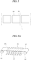
- FIG. 5 is a view illustrating a film on which a process is carried out by a roll fabrication apparatus having a structure illustrated in FIG 3 .
- a plurality of lighting apparatuses 100 are arranged in a line along a length direction of the film 201. All the processes illustrated in FIG. 4 are carried out on the film 201, and subsequent to the completion of all the processes, the film 201 is cut and divided into a plurality of lighting apparatuses 100.
- a cutting line (C) is formed in a width direction of the film 201.
- the cutting line (C) is formed along the sides of the lighting apparatuses 100 arranged in a length direction of the film 201, and the lighting apparatuses 100 are divided into each lighting apparatus along the cutting line (C) at the completion of the lighting apparatuses 100.
- the film 201 on which the first electrode 124 and the pads 123a, 123b are formed is supplied to the roll fabrication apparatus 200 illustrated in FIG. 3 (S102), and the mask 202 is disposed on an entire surface of the film 201 (S103).
- the deposition of the organic luminescent material is carried out in a state that two side edge regions of the film 201 illustrated in FIG. 5 are blocked, and the organic light emitting material is not deposited on the first outer portion (NA1) and the second outer portion (NA2) formed with the pads 123a, 123b to expose the pads 123a,123b to the outside, and it will be described in more detail.
- FIG. 6A is a view illustrating a specific structure of the organic material depositing portion of the roll fabrication apparatus illustrated in FIG 3 . Though not illustrated in the drawing, the structure of the metal deposition unit is also substantially the same.
- the organic material deposition unit of the roll fabrication apparatus includes a deposition member 280 configured to deposit an organic light emitting material to form a layer on the film 201 being transported between the first roll 210 for supplying the film 201 and the second roll 212 for collecting the film 201, and a shielding member 276 disposed between the film 201 and the deposition member 280.
- an organic light emitting material is deposited only on a part of the substrate using a mask formed of metal to form the organic light emitting layer 130. Therefore, when the lighting apparatus 100 is fabricated using the roll fabrication apparatus 200 as illustrated in FIG. 3 , a deposition process should be carried out in a state that an additional mask is disposed on an entire surface of the film 201 being transported, thereby complicating the fabrication apparatus as well as disallowing the rapid process.
- an additional mask may be provided on the supply roll and the collection roll, and then the process may be carried out while transporting the mask in synchronization with the film 201.
- additional mask supply roll and mask collection roll are required, and thus there is a problem of increasing facility cost as well as increasing a volume of the facility.
- the film 201 and the mask are not precisely synchronized, there is a problem that the organic light emitting layer 130 to be formed becomes defective.
- the shielding member 276 is provided between the film 201 and the deposition member 280 of the organic material deposition unit to cover an edge region of the film 310 so as not to deposit an organic material in this region during deposition. Since the first pad 123a and the second pad 123b are disposed in the edge region of the film 201, when the organic material is deposited in this region, the first electrode 123 and the second electrode 123b are covered by the organic light emitting layer 130 not to allow the external terminal to make electrical contact with the first pad 123a and the second pad 123b, thereby disallowing the lighting apparatus 100 to operate.
- the organic material is deposited only in a part of a region where the lighting apparatus is to be formed but the organic light emitting layer 130 is not deposited in a region formed where the first pad 123a and the second pad 123b is formed, and therefore, there is no problem in applying a voltage.
- the shielding member 276 is provided without using such a mask not to deposit the organic light emitting layer 130 in a region where the first pad 123a and the second pad 123b are disposed. In other words, when the organic material is deposited, the shielding member 276 covers only the edge region of the film 201 formed with the first pad 123a and the second pad 123b not to deposit the organic material on the first pad 123a and the second pad 123b.
- the shielding member 276 as a device having an opening portion 276a having a predetermined width formed of a material such as metal or the like is fixedly provided on the deposition member 280.
- a region formed with the lighting apparatus of the film 201 is exposed to the deposition member 280 through the opening portion 276a of the deposition member 276, and an organic material vaporized in the deposition member 280 is deposited in a region exposed through the opening portion 276a.
- organic material deposition unit of the roll fabrication apparatus of the present disclosure may be configured as illustrated in FIG. 6B .
- the film 201 on which the lighting apparatus 100 is formed may be deposited on a deposition drum 290 while being wound around the deposition drum 290.
- a shielding member 292 is provided along a circumferential surface of the deposition drum 290 to form an opening portion 292a and a region formed with the lighting apparatus of the film 201 is exposed to the outside through the opening portion 292a.
- a deposition member (not shown) may be disposed on a surface opposite to the opening portion 292a, and an organic material may be deposited on the exposed region of the film 201 through the opening portion 292a.
- a partial region of the organic light emitting layer 130 is processed (etched) by a laser to form the contact portion 129 in the organic light emitting portion 130 (S104).
- a metal is deposited by the metal deposition unit having the structure illustrated in FIGS. 6A and 6B in a state that an edge region of the film 201 is blocked by the shielding member to form the second electrode 126 (S105).
- the second electrode 126 is also formed on the contact portion 129 formed on the organic light emitting portion 130, and thus the second electrode 126 is electrically connected to the second pad 123b through the contact portion 129.
- the organic light emitting layer 130 and the second electrode 126 are formed by depositing an organic light emitting material and a metal using the shielding member 276. Therefore, the second electrode 126 is deposited only in a region corresponding to the open area 276a of the shielding member 276 but not deposited in a region blocked by the shielding member 276, and thus the second electrode 126 is not formed on the second pads 123a, 123b disposed on the second outer portion (NA2) corresponding to both side edge regions of the film 201, and as a result, the second electrode 126 is electrically connected to the second pad 123b.
- the contact portion 129 in which a partial region of the organic light emitting layer 130 is etched is formed on the organic light emitting layer 130, and the second electrode 126 is also formed within the contact portion 129, and thus the second electrode 126 is electrically connected to the second pad 123b through the contact portion 129.
- the second electrode 126 and the organic light emitting layer 130 are simultaneously etched by a laser to remove the second electrode 126 and the organic light emitting layer 130 to form an open region so as to disconnect the organic light emitting layer 130 along two side edge regions of the lighting apparatus 100 (SI06), and then the adhesive 118 is coated on the film 201 to adhere the protective film 170, thereby forming a plurality of lighting apparatuses 100 on the film 201 (S107, S108).
- the protective film may be formed of various materials.
- the protective film may be formed of a polymer such as PET or a thin metal foil.
- a non-flexible material such as glass may be used.
- the lighting apparatus 100 completed by cutting the film 201 is separated to complete each lighting apparatus 100.
- the cutting of the film 201 is carried out along a cutting line (C) formed along a width direction of the film 201.
- a region spaced apart from the cutting line of the film 201 by a predetermined distance will be the third and fourth outer portions (NA3, NA4).
- the organic light emitting layer 130 and the second electrode 126 are formed in a region excluding a partial region of the first and second outer portions (NA1, NA2) without using a mask.
- the organic light emitting layer 130 and the second electrode 126 are formed in the same region, the organic light emitting layer 130 is disposed between the second electrode 126 and the second pad 123b. Therefore, when the organic light emitting layer 130 and the second electrode 126 are formed without using a mask as in the present disclosure, the second electrode 126 and the second pad 123b are formed by interposing the organic light emitting layer 130 therebetween, and thus, the second electrode 126 and the second pad 123b are electrically insulated by the organic light emitting layer 130.
- an area of the organic light emitting layer 130 may be formed to be smaller than that of the second electrode 126 using a plurality of masks, and the second electrode 126 may be extended to an outer region of the organic light emitting layer 130 and disposed on an upper surface of the second pad 123b, thereby allowing the second electrode 126 in contact with the second pad 123b.
- a mask to be used may be added to complicate the structure of facilities, thereby increasing fabrication cost.
- the organic light emitting layer 130 and the second electrode 126 are formed without using a mask, and a part of the organic light emitting layer 130 is removed to form the contact portion 129 so as to electrically connect the second electrode 126 to the second pad 123b, and the second electrode 126 and the second pad 123b are electrically connected to each other through the contact portion 129.
- the organic light emitting layer 130 and the second electrode 126 are formed in the entire region of the lighting portion (EA) and the third and fourth outer portions (NA3, NA4) without using a mask, the organic light emitting layer 130 is exposed to the outside through a lateral end surface thereof, and moisture or air propagates into the lighting portion (EA) along the exposed organic light emitting layer 130 by the exposure of the organic light emitting layer 130.
- the organic light emitting layer 130 in a region spaced apart from the exposed lateral end surface by a predetermined distance is etched by a laser to form the open region 131 substantially parallel to the lateral end surface.
- the open region 130 is disconnected from the organic light emitting layer 130, it may be possible to prevent moisture and air infiltrated through the exposed organic light emitting layer 130 from being propagated into the lighting portion (EA).
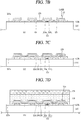
- FIGS. 7A through 7D are cross-sectional views illustrating a practical fabrication method of the lighting apparatus 100 according to the present disclosure
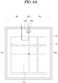
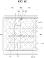
- FIGS. 8A through 8D are plan views illustrating a practical fabrication method of the lighting apparatus 100 according to the present disclosure.
- the fabrication process of the lighting apparatus 100 may be carried out on a plastic film on which a continuous process is carried out by a roll fabrication apparatus, but the present disclosure may not be limited thereto, but may be carried out on a glass mother substrate having a large area.
- the lighting apparatus 100 is fabricated using a single mask.
- a fabrication process of a plurality of lighting apparatuses is carried out in the film unit or mother substrate unit, but for the following description, it will be described in one lighting apparatus unit.
- a metal such as Al, Au, Cu, Ti, W, Mo or an alloy thereof is deposited and etched on a first substrate 110 formed of a soft material such as plastic or glass or the like to include a lighting portion (EA) and outer portions (NA1, NA2) so as to form an auxiliary electrode 122 configured with a single layer or a plurality of layers on the lighting portion (EA) and the outer portions (NA1, NA2).
- the auxiliary electrode 122 is disposed in a matrix shape in a horizontal direction and a vertical direction in a band shape set on an entire region of the lighting portion (EA) and a partial region of the outer portions (NA1, NA2), but the auxiliary electrode 122 may be disposed in a matrix shape, a mesh shape, a hexagonal shape, an octagonal shape or a circular shape.
- a transparent conductive material such as ITO or IZO is deposited and etched over an entire surface of the first substrate 110 to form a first electrode 124 disposed on the auxiliary electrode 122 of the lighting portion (EA) and the first outer portion (NA1), and form a first pad 123a and a second pad 123b on the second outer portion (NA2) and on the first outer portion (NA1) and the second outer portion (NA2), respectively.
- an insulating material such as SiNx or SiOx is deposited and etched on the lighting portion (EA) and the first and second outer portions (NA1, NA2) to form a protective layer 112.
- auxiliary electrode 122, first electrode 124, and first and second pads 123a, 123b may be formed by a continuous photo process on a roll fabrication apparatus or may be formed by a typical sheet-type photo process.
- an organic light emitting material is deposited on a partial region of the lighting portion (EA) and the first and second outer portions (NA1, NA2) of the first substrate 110 to form an organic light emitting layer 130.
- the formation of the organic light emitting layer 130 may be carried out by a roll fabrication apparatus having the structure illustrated in FIG. 3 .
- an organic light emitting material may be deposited to form the organic light emitting layer 130.
- both edge regions of the first substrate 110 namely, two side edge regions of the substrate 110, are are blocked, and thus the organic light emitting layer 130 is not formed in the two side edge regions of the first substrate 110, and the first pad 123a and the second pad 123b are not hidden by the organic light emitting layer 130 but exposed to the outside.
- the formation of the organic light emitting layer 130 may be formed by disposing a mask on a mother substrate formed with a plurality of lighting apparatuses, and then depositing an organic light emitting material.
- the contact portion 129 may be formed in a thin band shape having a predetermined length on the second outer portion (NA2) at an upper portion of the lighting apparatus 100, but the contact portion 129 is not limited to a specific shape or area, and may be configured in various shapes and areas.
- the contact portion 129 may be configured in various shapes and areas such as a circular shape or a polygonal shape.
- a metal such as Ca, Ba, Mg, Al or Ag is deposited on the organic light emitting layer 130 to form a second electrode 126.
- the second electrode 126 may also be deposited by a roll fabrication apparatus having the shielding member 276 as illustrated in FIGS. 6A and 6B . Accordingly, the second electrode 126 is formed only in a region formed with the organic light emitting layer 130, and thus the metal is not deposited on two side edge regions of the substrate 110.
- the second electrode 126 is not formed on the first pad 123a and the second pad 123b of the first and second outer portions (NA1, NA2) and the first pad 123a and the second pad 123b are exposed to the outside.
- the organic light emitting layer 130 and the second electrode 126 are not disposed in a partial region of the first and second outer portions (NA1, NA2), and thus the organic light emitting layer 130 and the second electrode 126 are not also disposed on the first pad 123a and the second pad 123b and the first pad 123a and the second pad 122b are exposed to the outside and electrically connected to an external signal source.
- the second electrode 126 is also formed inside the contact portion 129 formed on the organic light emitting layer 130, and thus the second electrode 126 is electrically connected to the second pad 123b through the contact portion 129.
- the organic light emitting layer 130 and the second electrode 126 are deposited on the roll fabrication apparatus having the shielding portion 276, the organic light emitting layer 130 and the second electrode 126 are sequentially deposition in the same region as illustrated in the drawing. Accordingly, the organic light emitting layer 130 is disposed between the second electrode 126 and the second pad 123b and thus the second electrode 126 and the second pad 123b are electrically insulated from each other. When a voltage applied thereto through the second pad 123b from the outside, the voltage is not applied to the second electrode 126, thereby not allowing the lighting apparatus 100 to operate.
- the second electrode 126 and the second pad 123b should be electrically connected to each other to apply a voltage to the second electrode 126.
- a part of the organic light emitting layer 130 is etched by a laser to form the contact portion 129, and the second electrode 126 and the second pad 123b are connected through the contact portion 129.
- the organic light emitting layer 130 and the second electrode 126 are formed using two masks such as a mask for forming the organic light emitting layer 130 and a mask for forming the second electrode 126 and the second pad 123b to connect the second electrode 126 to the second pad 123b.
- the organic light emitting layer 130 and the second electrode 126 are formed using two masks having open regions of different sizes such that the second electrode 126 is formed not only on a upper portion of the organic light emitting layer 130 but also on an upper portion of the second pad 123b, thereby connecting the second electrode 126 to the second pad 123b.
- an additional mask should be used, thereby increasing fabrication cost increases and complicating fabrication process.
- a part of the light emitting layer 130 is etched by a laser to form the contact portion 129.
- the second electrode 126 and the organic light emitting layer 130 are etched by a laser to form the open region 131 on the second electrode 126 and the organic light emitting layer 130.
- the open region 131 is formed in an inner region of two sides where the pads 123a, 123b of the lighting apparatus 100 are not formed, namely, in a region spaced apart from both the cutting lines (C) of the lighting apparatus 100 formed on the film 201 in FIG.
- an adhesive 118 formed of a photocurable adhesive material or thermosetting adhesive material is coated on the first substrate 110, and a second substrate 170 is placed thereon, and then the second substrate 170 is adhered thereto by curing the adhesive 118, and then the first substrate 110 and the second substrate 170 adhered to each other are cut to separate a completed lighting apparatus 100, thereby completing each lighting apparatus 100.
- a polymer film such as PET, a thin metal foil such as aluminum, glass, or the like may be used.
- the cutting of the substrates 110, 170 is carried out along a cutting line (C) formed along a width direction of the substrates 110, 170.
- the cutting of the substrates 110, 170 is carried out along a vertical direction of the sides of the substrates 110, 170 formed with the pads 123a, 123b, and thus the organic light emitting layer 130 and the second electrode 126 are exposed to the outside to a lateral end surface of the lighting apparatus 100 as illustrated in FIG. 2B .
- the cutting of the substrates 110, 170 may be carried out with various methods.
- the film 201 may be cut by a laser such as an Nd-YAG laser or a CO 2 laser or the substrates 110, 170 may be cut using a mechanical cutting tool.
- FIG. 9 is a view illustrating a lighting apparatus 300 according to a second embodiment of the present disclosure.
- the lighting apparatus 300 of this embodiment is configured with a first substrate 310 including a lighting portion (EA) for emitting actual light to output the light to the outside, and outer portions (NA1, NA2) at an outside thereof.
- the first substrate 310 is formed of plastic or glass having flexibility, and a first electrode 324 and a second electrode 326 are disposed on the first substrate 310, and an organic light emitting layer 330 is disposed between the first electrode 324 and the second electrode 326.
- a matrix-shaped auxiliary electrode 322 is disposed in a partial region of the lighting portion (EA) and the outer portions (NA1, NA2).
- a first outer portion (NA1) and a second outer portion (NA2) are disposed on an upper side and a lower side of the first substrate 310, respectively, and a first pad 323a is provided on the first outer portion (NA1) and a second pad 323b is disposed on the second outer portion (NA2).
- the organic light emitting layer 330 and the second electrode 326 are formed using the same mask, and thus the organic light emitting layer 330 and the second electrode 326 are formed in the same area on the first substrate 310. Accordingly, the organic light emitting layer 330 is disposed between the second pad 323b formed integrally with the first electrode 324 and the second electrode 326, and thus the second electrode 326 is electrically disconnected from the second pad 323b by the organic light emitting layer 330.
- a contact portion 329 from which a part of the organic light emitting layer 330 of the second outer portion (NA2) is removed by a laser or the like is formed, and the second electrode 326 is electrically connected to the second pad 322 through the contact portion 329, and a signal is applied to the second electrode 326 through the second pad 323b.
- the first pad 323a and the second pad 323b are formed on an upper and a lower edge regions of the first substrate 310, respectively, and a signal is applied from an upper side and a lower side of the lighting apparatus 300, and thus the signal may be quickly applied to the entire lighting apparatus 300 as compared with the lighting apparatus of the first embodiment illustrated in FIG. 1 in which only one first pad 323a and second pad 323b is formed, thereby allowing a quick drive of the lighting apparatus 300.
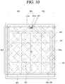
- FIG. 10 is a plan view illustrating the structure of a lighting apparatus 400 according to a third embodiment of the present disclosure.
- one first outer portion (NA1) and second outer portion (NA2) is disposed on an upper side of the first substrate 400. Furthermore, two contact portions 429 are formed on the second pad 423b disposed on the second outer portion (NA2), and thus the second electrode 426 and the second pad 423b are connected to each other through the two contact portions 429. As described above, this embodiment may be formed with two contact portions 429, thereby preventing a signal delay due to a contact resistance as compared with the structure in which one contact portion is formed.
- two contact portions 429 may be formed, but three or more contact portions 429 may also be formed. Furthermore, as illustrated in FIG. 9 , two or more second pads 423b may be formed on the first substrate 410, and a plurality of contact portions 429 may be formed on each of the second pads 423b.
- an organic light emitting material may be deposited on a substrate without using a mask to form a lighting apparatus.
- the organic light emitting layer and the second electrode may not be formed on a pad during the deposition of the organic light emitting layer and the second electrode by a roll fabrication apparatus having the shielding member, thereby forming a lighting apparatus.
- a part of the organic light emitting layer 130 may be etched with a laser to electrically connect the second electrode 126 to the second pad 123b, thereby not requiring the use of an additional mask.
- the organic light emitting layer 130 may be exposed to the outside, but an open region in parallel to the exposed side may be formed in a region spaced apart from the exposed side by a predetermined distance to disconnect the organic light emitting layer 130, preventing air or moisture from being propagated to the organic light emitting layer within the lighting portion.
Landscapes
- Physics & Mathematics (AREA)
- Optics & Photonics (AREA)
- Engineering & Computer Science (AREA)
- Manufacturing & Machinery (AREA)
- Electroluminescent Light Sources (AREA)
Claims (15)
- Appareil d'éclairage comportant :un premier substrat (110) comportant une portion d'éclairage (EA), une première portion extérieure (NA1) disposée sur un bord extérieur de la portion d'éclairage (EA), et une seconde portion extérieure (NA3, NA4) disposée le long d'une seconde direction perpendiculaire à la première partie extérieure (NA1) ;un dispositif électroluminescent organique comportant une première électrode (124), une couche électroluminescente organique (130) et une seconde électrode (126) agencée dans la partie d'éclairage (EA) et dans une zone partielle des première et seconde parties extérieures (NA3, NA4) sur le premier substrat (110) ; etune première pastille (123a) et une seconde pastille (123b) disposées sur la première partie extérieure (NA1) et connectées à la première électrode et à la seconde électrode pour appliquer une tension à la première électrode (124) et à la seconde électrode (126),dans lequel la couche électroluminescente organique (130) et la seconde électrode (126) ne sont pas formées dans une zone partielle de la première partie extérieure (NA1) dans laquelle la première pastille et la seconde pastille sont disposées pour ne pas exposer la couche électroluminescente organique (130) et la seconde électrode (126) à un extérieur le long de la première partie extérieure (NA1) et sont formées sur la seconde partie extérieure (NA3) complète pour exposer la couche électroluminescente organique (130) et la seconde électrode (126) à l'extérieur à travers une surface d'extrémité latérale de la seconde partie extérieure (NA3), et une zone ouverte (131) est formée sur la seconde électrode (126) et la couche électroluminescente organique (130) dans une zone espacée de la surface d'extrémité latérale par une distance prédéterminée le long de la surface d'extrémité latérale de la seconde partie extérieure (NA3) pour déconnecter la couche électroluminescente organique (130).
- Appareil d'éclairage selon la revendication 1, dans lequel la seconde pastille (123b) est électriquement connectée à la seconde électrode (126) via une partie de contact (129, 329, 429) formée sur la même couche que celle de la première pastille (123a) et formée à travers la couche électroluminescente organique (130).
- Appareil d'éclairage selon la revendication 1 ou 2, dans lequel la couche électroluminescente organique (130) et la seconde électrode (126) ont la même aire, et la couche électroluminescente organique (130) est disposée entre la seconde électrode (126) et la seconde pastille (123b).
- Appareil d'éclairage selon la revendication 2 ou 3, dans lequel la partie de contact (129, 329, 429) est une zone dans laquelle la couche électroluminescente organique (130) est retirée par un laser dans une zone où la couche électroluminescente organique recouvre la seconde électrode.
- Appareil d'éclairage selon la revendication 2, 3 ou 4, dans lequel la partie de contact (129, 329, 429) est formée en forme de bande ou la partie de contact (129, 329, 429) est formée en forme de trou.
- Appareil d'éclairage selon l'une quelconque des revendications précédentes, dans lequel la première pastille (123a) et la seconde pastille (123b) sont disposées dans une zone de bord supérieure ou une zone de bord latéral supérieure et inférieure du premier substrat (110).
- Appareil d'éclairage selon l'une quelconque des revendications précédentes, dans lequel le premier substrat (110) est formé d'un film souple ou le premier substrat (110) est formé de verre.
- Appareil d'éclairage selon l'une quelconque des revendications précédentes, comportant en outre un second substrat (170) adhérant au premier substrat (110) par un adhésif (118).
- Appareil d'éclairage selon la revendication 8, dans lequel le second substrat (170) est formé d'un matériau choisi parmi le groupe constitué d'un film polymère, d'une feuille de métal et de verre.
- Appareil d'éclairage selon l'une quelconque des revendications précédentes, comportant en outre une électrode auxiliaire (122) disposée dans la partie d'éclairage (EA) et les première et seconde parties extérieures (NA1, NA3) du premier substrat (110), l'électrode auxiliaire (122) étant connectée à la première électrode (124).
- Appareil d'éclairage selon la revendication 10, dans lequel l'électrode auxiliaire (122) est disposée avec une forme de matrice, une forme de treillis, une forme octogonale, une forme hexagonale ou une forme circulaire à l'intérieur de la partie d'éclairage (EA) avec une largeur prédéfinie.
- Procédé de fabrication d'un appareil d'éclairage selon la revendication 1, le procédé comportant les étapes consistant à :former (S101) une électrode auxiliaire (122), une première électrode (124), une première pastille (123a) et une seconde pastille (123b) dans une pluralité de zones d'appareil d'éclairage agencées le long d'une direction de longueur d'un premier substrat (110) ;déposer entièrement (S103) un matériau électroluminescent organique sur les zones d'appareil d'éclairage pour former une couche électroluminescente organique (130) ; déposer entièrement (S105) un métal sur les zones d'appareil d'éclairage pour former une seconde électrode (126) sur la couche électroluminescente organique (130) ;retirer la seconde électrode (126) et la couche électroluminescente organique (130) dans un bord des zones d'appareil d'éclairage le long d'une direction de largeur du premier substrat (110) pour former une zone ouverte (131) ; etfaire adhérer (S108) un second substrat (170) sur la seconde électrode (126) par un adhésif (118).
- Procédé selon la revendication 12, comportant en outre le retrait de la couche électroluminescente organique (130) pour former une partie de contact (129, 329, 429) pour connecter électriquement la seconde électrode (126) à la seconde pastille (123b).
- Procédé selon la revendication 13, dans lequel la formation de la partie de contact (129, 329, 429) et/ou la formation de la zone ouverte (131) comporte la gravure de la couche électroluminescente organique (130) par un laser.
- Procédé selon la revendication 12, 13 ou 14, dans lequel le matériau électroluminescent organique et le métal sont déposés par un appareil de fabrication à rouleaux, l'appareil de fabrication à rouleaux (200) comporte de préférence un élément de protection (276) pour bloquer une zone de formation de première pastille et de seconde pastille pour déposer le matériau électroluminescent organique et le métal sur un film en excluant la zone de formation de première pastille et de seconde pastille.
Applications Claiming Priority (1)
| Application Number | Priority Date | Filing Date | Title |
|---|---|---|---|
| KR1020160182831A KR102712304B1 (ko) | 2016-12-29 | 2016-12-29 | 유기발광소자를 이용한 조명장치 및 그 제조방법 |
Publications (2)
| Publication Number | Publication Date |
|---|---|
| EP3349267A1 EP3349267A1 (fr) | 2018-07-18 |
| EP3349267B1 true EP3349267B1 (fr) | 2021-09-15 |
Family
ID=60915361
Family Applications (1)
| Application Number | Title | Priority Date | Filing Date |
|---|---|---|---|
| EP17210695.7A Active EP3349267B1 (fr) | 2016-12-29 | 2017-12-27 | Appareil d'éclairage faisant appel à un dispositif électroluminescent organique et son procédé de fabrication |
Country Status (4)
| Country | Link |
|---|---|
| US (1) | US10553832B2 (fr) |
| EP (1) | EP3349267B1 (fr) |
| KR (1) | KR102712304B1 (fr) |
| CN (1) | CN108260259B (fr) |
Families Citing this family (6)
| Publication number | Priority date | Publication date | Assignee | Title |
|---|---|---|---|---|
| KR102581656B1 (ko) * | 2016-12-29 | 2023-09-21 | 엘지디스플레이 주식회사 | 유기발광소자를 이용한 조명장치 및 그 제조방법 |
| KR102589995B1 (ko) * | 2018-08-27 | 2023-10-13 | 엘지디스플레이 주식회사 | 유기 발광 소자를 이용한 조명 장치 |
| KR102601826B1 (ko) * | 2018-12-31 | 2023-11-13 | 엘지디스플레이 주식회사 | 유기 조명 장치 |
| US11818912B2 (en) * | 2019-01-04 | 2023-11-14 | Apple Inc. | Organic light-emitting diode display panels with moisture blocking structures |
| KR20220162896A (ko) | 2021-06-01 | 2022-12-09 | 삼성디스플레이 주식회사 | 레이저 가공 장치 및 레이저 가공 방법 |
| CN115000139B (zh) * | 2022-05-31 | 2025-02-14 | 武汉华星光电半导体显示技术有限公司 | 显示面板与显示装置 |
Family Cites Families (7)
| Publication number | Priority date | Publication date | Assignee | Title |
|---|---|---|---|---|
| JP5743609B2 (ja) | 2011-02-28 | 2015-07-01 | 株式会社カネカ | 有機el発光素子 |
| KR101970675B1 (ko) * | 2011-08-04 | 2019-04-19 | 가부시키가이샤 한도오따이 에네루기 켄큐쇼 | 발광 장치 및 조명 장치 |
| US9508959B2 (en) * | 2012-05-10 | 2016-11-29 | Kaneka Corporation | Organic EL device and method for manufacturing same |
| CN104982092B (zh) * | 2013-02-07 | 2017-04-05 | 松下知识产权经营株式会社 | 有机电致发光元件以及照明装置 |
| JP6163334B2 (ja) | 2013-03-27 | 2017-07-12 | 株式会社カネカ | 有機el装置 |
| WO2014188895A1 (fr) * | 2013-05-21 | 2014-11-27 | Semiconductor Energy Laboratory Co., Ltd. | Dispositif électroluminescent et appareil photo |
| JP6053221B1 (ja) * | 2015-10-20 | 2016-12-27 | 住友化学株式会社 | 有機el素子及びその製造方法 |
-
2016
- 2016-12-29 KR KR1020160182831A patent/KR102712304B1/ko active Active
-
2017
- 2017-09-14 US US15/704,760 patent/US10553832B2/en active Active
- 2017-12-19 CN CN201711372789.3A patent/CN108260259B/zh active Active
- 2017-12-27 EP EP17210695.7A patent/EP3349267B1/fr active Active
Also Published As
| Publication number | Publication date |
|---|---|
| US10553832B2 (en) | 2020-02-04 |
| US20180190947A1 (en) | 2018-07-05 |
| KR102712304B1 (ko) | 2024-09-30 |
| KR20180077939A (ko) | 2018-07-09 |
| EP3349267A1 (fr) | 2018-07-18 |
| CN108260259B (zh) | 2020-03-03 |
| CN108260259A (zh) | 2018-07-06 |
Similar Documents
| Publication | Publication Date | Title |
|---|---|---|
| EP3349267B1 (fr) | Appareil d'éclairage faisant appel à un dispositif électroluminescent organique et son procédé de fabrication | |
| EP3316333B1 (fr) | Appareil d'éclairage utilisant un dispositif électroluminescent organique et son procédé de fabrication | |
| EP3346499B1 (fr) | Appareil d'éclairage utilisant une diode électroluminescente organique et son procédé de fabrication | |
| EP3331039B1 (fr) | Appareil d'éclairage utilisant une diode électroluminescente organique et son procédé de fabrication | |
| EP3327816B1 (fr) | Appareil d'éclairage faisant appel à un dispositif électroluminescent organique et son procédé de fabrication | |
| EP3333894B1 (fr) | Appareil lumineux utilisant une diode électroluminescente organique et son procédé de fabrication | |
| EP3333925B1 (fr) | Appareil d'éclairage faisant appel à une diode électroluminescente organique | |
| EP3343661B1 (fr) | Appareil d'éclairage utilisant un dispositif électroluminescent organique et son procédé de fabrication | |
| EP3327807B1 (fr) | Appareil et procédé de fabrication d'appareil d'éclairage |
Legal Events
| Date | Code | Title | Description |
|---|---|---|---|
| PUAI | Public reference made under article 153(3) epc to a published international application that has entered the european phase |
Free format text: ORIGINAL CODE: 0009012 |
|
| STAA | Information on the status of an ep patent application or granted ep patent |
Free format text: STATUS: REQUEST FOR EXAMINATION WAS MADE |
|
| 17P | Request for examination filed |
Effective date: 20171227 |
|
| AK | Designated contracting states |
Kind code of ref document: A1 Designated state(s): AL AT BE BG CH CY CZ DE DK EE ES FI FR GB GR HR HU IE IS IT LI LT LU LV MC MK MT NL NO PL PT RO RS SE SI SK SM TR |
|
| AX | Request for extension of the european patent |
Extension state: BA ME |
|
| GRAP | Despatch of communication of intention to grant a patent |
Free format text: ORIGINAL CODE: EPIDOSNIGR1 |
|
| STAA | Information on the status of an ep patent application or granted ep patent |
Free format text: STATUS: GRANT OF PATENT IS INTENDED |
|
| INTG | Intention to grant announced |
Effective date: 20210421 |
|
| GRAS | Grant fee paid |
Free format text: ORIGINAL CODE: EPIDOSNIGR3 |
|
| GRAA | (expected) grant |
Free format text: ORIGINAL CODE: 0009210 |
|
| STAA | Information on the status of an ep patent application or granted ep patent |
Free format text: STATUS: THE PATENT HAS BEEN GRANTED |
|
| AK | Designated contracting states |
Kind code of ref document: B1 Designated state(s): AL AT BE BG CH CY CZ DE DK EE ES FI FR GB GR HR HU IE IS IT LI LT LU LV MC MK MT NL NO PL PT RO RS SE SI SK SM TR |
|
| REG | Reference to a national code |
Ref country code: CH Ref legal event code: EP |
|
| REG | Reference to a national code |
Ref country code: DE Ref legal event code: R096 Ref document number: 602017045989 Country of ref document: DE |
|
| REG | Reference to a national code |
Ref country code: IE Ref legal event code: FG4D |
|
| REG | Reference to a national code |
Ref country code: AT Ref legal event code: REF Ref document number: 1431222 Country of ref document: AT Kind code of ref document: T Effective date: 20211015 |
|
| REG | Reference to a national code |
Ref country code: LT Ref legal event code: MG9D |
|
| REG | Reference to a national code |
Ref country code: NL Ref legal event code: MP Effective date: 20210915 |
|
| PG25 | Lapsed in a contracting state [announced via postgrant information from national office to epo] |
Ref country code: BG Free format text: LAPSE BECAUSE OF FAILURE TO SUBMIT A TRANSLATION OF THE DESCRIPTION OR TO PAY THE FEE WITHIN THE PRESCRIBED TIME-LIMIT Effective date: 20211215 Ref country code: LT Free format text: LAPSE BECAUSE OF FAILURE TO SUBMIT A TRANSLATION OF THE DESCRIPTION OR TO PAY THE FEE WITHIN THE PRESCRIBED TIME-LIMIT Effective date: 20210915 Ref country code: NO Free format text: LAPSE BECAUSE OF FAILURE TO SUBMIT A TRANSLATION OF THE DESCRIPTION OR TO PAY THE FEE WITHIN THE PRESCRIBED TIME-LIMIT Effective date: 20211215 Ref country code: FI Free format text: LAPSE BECAUSE OF FAILURE TO SUBMIT A TRANSLATION OF THE DESCRIPTION OR TO PAY THE FEE WITHIN THE PRESCRIBED TIME-LIMIT Effective date: 20210915 Ref country code: RS Free format text: LAPSE BECAUSE OF FAILURE TO SUBMIT A TRANSLATION OF THE DESCRIPTION OR TO PAY THE FEE WITHIN THE PRESCRIBED TIME-LIMIT Effective date: 20210915 Ref country code: SE Free format text: LAPSE BECAUSE OF FAILURE TO SUBMIT A TRANSLATION OF THE DESCRIPTION OR TO PAY THE FEE WITHIN THE PRESCRIBED TIME-LIMIT Effective date: 20210915 Ref country code: HR Free format text: LAPSE BECAUSE OF FAILURE TO SUBMIT A TRANSLATION OF THE DESCRIPTION OR TO PAY THE FEE WITHIN THE PRESCRIBED TIME-LIMIT Effective date: 20210915 |
|
| REG | Reference to a national code |
Ref country code: AT Ref legal event code: MK05 Ref document number: 1431222 Country of ref document: AT Kind code of ref document: T Effective date: 20210915 |
|
| PG25 | Lapsed in a contracting state [announced via postgrant information from national office to epo] |
Ref country code: LV Free format text: LAPSE BECAUSE OF FAILURE TO SUBMIT A TRANSLATION OF THE DESCRIPTION OR TO PAY THE FEE WITHIN THE PRESCRIBED TIME-LIMIT Effective date: 20210915 Ref country code: GR Free format text: LAPSE BECAUSE OF FAILURE TO SUBMIT A TRANSLATION OF THE DESCRIPTION OR TO PAY THE FEE WITHIN THE PRESCRIBED TIME-LIMIT Effective date: 20211216 |
|
| PG25 | Lapsed in a contracting state [announced via postgrant information from national office to epo] |
Ref country code: AT Free format text: LAPSE BECAUSE OF FAILURE TO SUBMIT A TRANSLATION OF THE DESCRIPTION OR TO PAY THE FEE WITHIN THE PRESCRIBED TIME-LIMIT Effective date: 20210915 |
|
| PG25 | Lapsed in a contracting state [announced via postgrant information from national office to epo] |
Ref country code: IS Free format text: LAPSE BECAUSE OF FAILURE TO SUBMIT A TRANSLATION OF THE DESCRIPTION OR TO PAY THE FEE WITHIN THE PRESCRIBED TIME-LIMIT Effective date: 20220115 Ref country code: SM Free format text: LAPSE BECAUSE OF FAILURE TO SUBMIT A TRANSLATION OF THE DESCRIPTION OR TO PAY THE FEE WITHIN THE PRESCRIBED TIME-LIMIT Effective date: 20210915 Ref country code: SK Free format text: LAPSE BECAUSE OF FAILURE TO SUBMIT A TRANSLATION OF THE DESCRIPTION OR TO PAY THE FEE WITHIN THE PRESCRIBED TIME-LIMIT Effective date: 20210915 Ref country code: RO Free format text: LAPSE BECAUSE OF FAILURE TO SUBMIT A TRANSLATION OF THE DESCRIPTION OR TO PAY THE FEE WITHIN THE PRESCRIBED TIME-LIMIT Effective date: 20210915 Ref country code: PT Free format text: LAPSE BECAUSE OF FAILURE TO SUBMIT A TRANSLATION OF THE DESCRIPTION OR TO PAY THE FEE WITHIN THE PRESCRIBED TIME-LIMIT Effective date: 20220117 Ref country code: PL Free format text: LAPSE BECAUSE OF FAILURE TO SUBMIT A TRANSLATION OF THE DESCRIPTION OR TO PAY THE FEE WITHIN THE PRESCRIBED TIME-LIMIT Effective date: 20210915 Ref country code: NL Free format text: LAPSE BECAUSE OF FAILURE TO SUBMIT A TRANSLATION OF THE DESCRIPTION OR TO PAY THE FEE WITHIN THE PRESCRIBED TIME-LIMIT Effective date: 20210915 Ref country code: ES Free format text: LAPSE BECAUSE OF FAILURE TO SUBMIT A TRANSLATION OF THE DESCRIPTION OR TO PAY THE FEE WITHIN THE PRESCRIBED TIME-LIMIT Effective date: 20210915 Ref country code: EE Free format text: LAPSE BECAUSE OF FAILURE TO SUBMIT A TRANSLATION OF THE DESCRIPTION OR TO PAY THE FEE WITHIN THE PRESCRIBED TIME-LIMIT Effective date: 20210915 Ref country code: CZ Free format text: LAPSE BECAUSE OF FAILURE TO SUBMIT A TRANSLATION OF THE DESCRIPTION OR TO PAY THE FEE WITHIN THE PRESCRIBED TIME-LIMIT Effective date: 20210915 Ref country code: AL Free format text: LAPSE BECAUSE OF FAILURE TO SUBMIT A TRANSLATION OF THE DESCRIPTION OR TO PAY THE FEE WITHIN THE PRESCRIBED TIME-LIMIT Effective date: 20210915 |
|
| REG | Reference to a national code |
Ref country code: DE Ref legal event code: R097 Ref document number: 602017045989 Country of ref document: DE |
|
| PLBE | No opposition filed within time limit |
Free format text: ORIGINAL CODE: 0009261 |
|
| STAA | Information on the status of an ep patent application or granted ep patent |
Free format text: STATUS: NO OPPOSITION FILED WITHIN TIME LIMIT |
|
| PG25 | Lapsed in a contracting state [announced via postgrant information from national office to epo] |
Ref country code: MC Free format text: LAPSE BECAUSE OF FAILURE TO SUBMIT A TRANSLATION OF THE DESCRIPTION OR TO PAY THE FEE WITHIN THE PRESCRIBED TIME-LIMIT Effective date: 20210915 Ref country code: DK Free format text: LAPSE BECAUSE OF FAILURE TO SUBMIT A TRANSLATION OF THE DESCRIPTION OR TO PAY THE FEE WITHIN THE PRESCRIBED TIME-LIMIT Effective date: 20210915 |
|
| REG | Reference to a national code |
Ref country code: CH Ref legal event code: PL |
|
| 26N | No opposition filed |
Effective date: 20220616 |
|
| PG25 | Lapsed in a contracting state [announced via postgrant information from national office to epo] |
Ref country code: SI Free format text: LAPSE BECAUSE OF FAILURE TO SUBMIT A TRANSLATION OF THE DESCRIPTION OR TO PAY THE FEE WITHIN THE PRESCRIBED TIME-LIMIT Effective date: 20210915 |
|
| REG | Reference to a national code |
Ref country code: BE Ref legal event code: MM Effective date: 20211231 |
|
| PG25 | Lapsed in a contracting state [announced via postgrant information from national office to epo] |
Ref country code: LU Free format text: LAPSE BECAUSE OF NON-PAYMENT OF DUE FEES Effective date: 20211227 Ref country code: IE Free format text: LAPSE BECAUSE OF NON-PAYMENT OF DUE FEES Effective date: 20211227 |
|
| REG | Reference to a national code |
Ref country code: DE Ref legal event code: R079 Ref document number: 602017045989 Country of ref document: DE Free format text: PREVIOUS MAIN CLASS: H01L0051520000 Ipc: H10K0050800000 |
|
| PG25 | Lapsed in a contracting state [announced via postgrant information from national office to epo] |
Ref country code: FR Free format text: LAPSE BECAUSE OF NON-PAYMENT OF DUE FEES Effective date: 20211231 Ref country code: BE Free format text: LAPSE BECAUSE OF NON-PAYMENT OF DUE FEES Effective date: 20211231 |
|
| PG25 | Lapsed in a contracting state [announced via postgrant information from national office to epo] |
Ref country code: LI Free format text: LAPSE BECAUSE OF NON-PAYMENT OF DUE FEES Effective date: 20211231 Ref country code: CH Free format text: LAPSE BECAUSE OF NON-PAYMENT OF DUE FEES Effective date: 20211231 |
|
| PG25 | Lapsed in a contracting state [announced via postgrant information from national office to epo] |
Ref country code: IT Free format text: LAPSE BECAUSE OF FAILURE TO SUBMIT A TRANSLATION OF THE DESCRIPTION OR TO PAY THE FEE WITHIN THE PRESCRIBED TIME-LIMIT Effective date: 20210915 |
|
| PG25 | Lapsed in a contracting state [announced via postgrant information from national office to epo] |
Ref country code: HU Free format text: LAPSE BECAUSE OF FAILURE TO SUBMIT A TRANSLATION OF THE DESCRIPTION OR TO PAY THE FEE WITHIN THE PRESCRIBED TIME-LIMIT; INVALID AB INITIO Effective date: 20171227 |
|
| PG25 | Lapsed in a contracting state [announced via postgrant information from national office to epo] |
Ref country code: CY Free format text: LAPSE BECAUSE OF FAILURE TO SUBMIT A TRANSLATION OF THE DESCRIPTION OR TO PAY THE FEE WITHIN THE PRESCRIBED TIME-LIMIT Effective date: 20210915 |
|
| PG25 | Lapsed in a contracting state [announced via postgrant information from national office to epo] |
Ref country code: MK Free format text: LAPSE BECAUSE OF FAILURE TO SUBMIT A TRANSLATION OF THE DESCRIPTION OR TO PAY THE FEE WITHIN THE PRESCRIBED TIME-LIMIT Effective date: 20210915 |
|
| PG25 | Lapsed in a contracting state [announced via postgrant information from national office to epo] |
Ref country code: MT Free format text: LAPSE BECAUSE OF FAILURE TO SUBMIT A TRANSLATION OF THE DESCRIPTION OR TO PAY THE FEE WITHIN THE PRESCRIBED TIME-LIMIT Effective date: 20210915 |
|
| PG25 | Lapsed in a contracting state [announced via postgrant information from national office to epo] |
Ref country code: TR Free format text: LAPSE BECAUSE OF FAILURE TO SUBMIT A TRANSLATION OF THE DESCRIPTION OR TO PAY THE FEE WITHIN THE PRESCRIBED TIME-LIMIT Effective date: 20210915 |
|
| PGFP | Annual fee paid to national office [announced via postgrant information from national office to epo] |
Ref country code: DE Payment date: 20251020 Year of fee payment: 9 |
|
| PGFP | Annual fee paid to national office [announced via postgrant information from national office to epo] |
Ref country code: GB Payment date: 20251023 Year of fee payment: 9 |