EP3349870B1 - Moteur de jeu sur une puce - Google Patents
Moteur de jeu sur une puce Download PDFInfo
- Publication number
- EP3349870B1 EP3349870B1 EP16775106.4A EP16775106A EP3349870B1 EP 3349870 B1 EP3349870 B1 EP 3349870B1 EP 16775106 A EP16775106 A EP 16775106A EP 3349870 B1 EP3349870 B1 EP 3349870B1
- Authority
- EP
- European Patent Office
- Prior art keywords
- chip
- game engine
- engine
- processing unit
- game
- Prior art date
- Legal status (The legal status is an assumption and is not a legal conclusion. Google has not performed a legal analysis and makes no representation as to the accuracy of the status listed.)
- Active
Links
Images




Classifications
-
- G—PHYSICS
- G06—COMPUTING OR CALCULATING; COUNTING
- G06T—IMAGE DATA PROCESSING OR GENERATION, IN GENERAL
- G06T15/00—Three-dimensional [3D] image rendering
- G06T15/005—General purpose rendering architectures
-
- A—HUMAN NECESSITIES
- A63—SPORTS; GAMES; AMUSEMENTS
- A63F—CARD, BOARD, OR ROULETTE GAMES; INDOOR GAMES USING SMALL MOVING PLAYING BODIES; VIDEO GAMES; GAMES NOT OTHERWISE PROVIDED FOR
- A63F13/00—Video games, i.e. games using an electronically generated display having two or more dimensions
- A63F13/50—Controlling the output signals based on the game progress
- A63F13/52—Controlling the output signals based on the game progress involving aspects of the displayed game scene
-
- G—PHYSICS
- G06—COMPUTING OR CALCULATING; COUNTING
- G06F—ELECTRIC DIGITAL DATA PROCESSING
- G06F15/00—Digital computers in general; Data processing equipment in general
- G06F15/76—Architectures of general purpose stored program computers
- G06F15/80—Architectures of general purpose stored program computers comprising an array of processing units with common control, e.g. single instruction multiple data processors
-
- G—PHYSICS
- G06—COMPUTING OR CALCULATING; COUNTING
- G06T—IMAGE DATA PROCESSING OR GENERATION, IN GENERAL
- G06T15/00—Three-dimensional [3D] image rendering
- G06T15/06—Ray-tracing
-
- H—ELECTRICITY
- H10—SEMICONDUCTOR DEVICES; ELECTRIC SOLID-STATE DEVICES NOT OTHERWISE PROVIDED FOR
- H10W—GENERIC PACKAGES, INTERCONNECTIONS, CONNECTORS OR OTHER CONSTRUCTIONAL DETAILS OF DEVICES COVERED BY CLASS H10
- H10W90/00—Package configurations
-
- A—HUMAN NECESSITIES
- A63—SPORTS; GAMES; AMUSEMENTS
- A63F—CARD, BOARD, OR ROULETTE GAMES; INDOOR GAMES USING SMALL MOVING PLAYING BODIES; VIDEO GAMES; GAMES NOT OTHERWISE PROVIDED FOR
- A63F2300/00—Features of games using an electronically generated display having two or more dimensions, e.g. on a television screen, showing representations related to the game
- A63F2300/20—Features of games using an electronically generated display having two or more dimensions, e.g. on a television screen, showing representations related to the game characterised by details of the game platform
- A63F2300/203—Image generating hardware
-
- A—HUMAN NECESSITIES
- A63—SPORTS; GAMES; AMUSEMENTS
- A63F—CARD, BOARD, OR ROULETTE GAMES; INDOOR GAMES USING SMALL MOVING PLAYING BODIES; VIDEO GAMES; GAMES NOT OTHERWISE PROVIDED FOR
- A63F2300/00—Features of games using an electronically generated display having two or more dimensions, e.g. on a television screen, showing representations related to the game
- A63F2300/20—Features of games using an electronically generated display having two or more dimensions, e.g. on a television screen, showing representations related to the game characterised by details of the game platform
- A63F2300/209—Features of games using an electronically generated display having two or more dimensions, e.g. on a television screen, showing representations related to the game characterised by details of the game platform characterized by low level software layer, relating to hardware management, e.g. Operating System, Application Programming Interface
-
- H—ELECTRICITY
- H10—SEMICONDUCTOR DEVICES; ELECTRIC SOLID-STATE DEVICES NOT OTHERWISE PROVIDED FOR
- H10W—GENERIC PACKAGES, INTERCONNECTIONS, CONNECTORS OR OTHER CONSTRUCTIONAL DETAILS OF DEVICES COVERED BY CLASS H10
- H10W70/00—Package substrates; Interposers; Redistribution layers [RDL]
- H10W70/60—Insulating or insulated package substrates; Interposers; Redistribution layers
-
- H—ELECTRICITY
- H10—SEMICONDUCTOR DEVICES; ELECTRIC SOLID-STATE DEVICES NOT OTHERWISE PROVIDED FOR
- H10W—GENERIC PACKAGES, INTERCONNECTIONS, CONNECTORS OR OTHER CONSTRUCTIONAL DETAILS OF DEVICES COVERED BY CLASS H10
- H10W70/00—Package substrates; Interposers; Redistribution layers [RDL]
- H10W70/60—Insulating or insulated package substrates; Interposers; Redistribution layers
- H10W70/62—Insulating or insulated package substrates; Interposers; Redistribution layers characterised by their interconnections
- H10W70/63—Vias, e.g. via plugs
-
- H—ELECTRICITY
- H10—SEMICONDUCTOR DEVICES; ELECTRIC SOLID-STATE DEVICES NOT OTHERWISE PROVIDED FOR
- H10W—GENERIC PACKAGES, INTERCONNECTIONS, CONNECTORS OR OTHER CONSTRUCTIONAL DETAILS OF DEVICES COVERED BY CLASS H10
- H10W72/00—Interconnections or connectors in packages
- H10W72/071—Connecting or disconnecting
- H10W72/072—Connecting or disconnecting of bump connectors
- H10W72/07251—Connecting or disconnecting of bump connectors characterised by changes in properties of the bump connectors during connecting
- H10W72/07254—Connecting or disconnecting of bump connectors characterised by changes in properties of the bump connectors during connecting changes in dispositions
-
- H—ELECTRICITY
- H10—SEMICONDUCTOR DEVICES; ELECTRIC SOLID-STATE DEVICES NOT OTHERWISE PROVIDED FOR
- H10W—GENERIC PACKAGES, INTERCONNECTIONS, CONNECTORS OR OTHER CONSTRUCTIONAL DETAILS OF DEVICES COVERED BY CLASS H10
- H10W72/00—Interconnections or connectors in packages
- H10W72/20—Bump connectors, e.g. solder bumps or copper pillars; Dummy bumps; Thermal bumps
- H10W72/241—Dispositions, e.g. layouts
- H10W72/247—Dispositions of multiple bumps
-
- H—ELECTRICITY
- H10—SEMICONDUCTOR DEVICES; ELECTRIC SOLID-STATE DEVICES NOT OTHERWISE PROVIDED FOR
- H10W—GENERIC PACKAGES, INTERCONNECTIONS, CONNECTORS OR OTHER CONSTRUCTIONAL DETAILS OF DEVICES COVERED BY CLASS H10
- H10W90/00—Package configurations
- H10W90/20—Configurations of stacked chips
- H10W90/297—Configurations of stacked chips characterised by the through-semiconductor vias [TSVs] in the stacked chips
-
- H—ELECTRICITY
- H10—SEMICONDUCTOR DEVICES; ELECTRIC SOLID-STATE DEVICES NOT OTHERWISE PROVIDED FOR
- H10W—GENERIC PACKAGES, INTERCONNECTIONS, CONNECTORS OR OTHER CONSTRUCTIONAL DETAILS OF DEVICES COVERED BY CLASS H10
- H10W90/00—Package configurations
- H10W90/701—Package configurations characterised by the relative positions of pads or connectors relative to package parts
- H10W90/721—Package configurations characterised by the relative positions of pads or connectors relative to package parts of bump connectors
- H10W90/722—Package configurations characterised by the relative positions of pads or connectors relative to package parts of bump connectors between stacked chips
-
- H—ELECTRICITY
- H10—SEMICONDUCTOR DEVICES; ELECTRIC SOLID-STATE DEVICES NOT OTHERWISE PROVIDED FOR
- H10W—GENERIC PACKAGES, INTERCONNECTIONS, CONNECTORS OR OTHER CONSTRUCTIONAL DETAILS OF DEVICES COVERED BY CLASS H10
- H10W90/00—Package configurations
- H10W90/701—Package configurations characterised by the relative positions of pads or connectors relative to package parts
- H10W90/721—Package configurations characterised by the relative positions of pads or connectors relative to package parts of bump connectors
- H10W90/724—Package configurations characterised by the relative positions of pads or connectors relative to package parts of bump connectors between a chip and a stacked insulating package substrate, interposer or RDL
Definitions
- the present disclosure relates to an electronic chip or chip assembly.
- the present disclosure relates to a game engine implemented on an electronic chip or chip assembly in hardware.
- the present disclosure may also relate to a system on chip or system in package.
- Game engines play an increasingly important role in graphics applications.
- One major task of a software game engine is to provide the most realistic and highest quality of graphics possible at a real-time performance.
- a software game engine is typically provided as computer-executable code that is executed on a central processing unit (CPU).
- the game engine may typically run on a processor or microprocessor of a computing device, such as a CPU of a personal computer, a console, a mobile phone or a tablet.
- performance of the CPU may determine the performance of a software game engine.
- the software game engine may also access a graphics processing unit (GPU).
- the GPU can render lists of individual objects with a very high performance to graphics memory or video memory.
- a computer graphics scene may include a large number of objects with characteristics related to their position and orientation, behavior, material properties and the like.
- the game engine needs to consider the whole scene, which may often contain millions of objects that are to be rendered to the screen. For example, the game engine may consider the behavior and interaction of light with individual objects and between the objects of the scene.
- the software game engine may balance a hardly noticeable loss of quality with improved performance.
- One way of doing so is by dividing individual tasks into sub-tasks, specifically those which can be performed efficiently on a GPU. Graphics tasks could be parallelized on multiple CPUs.
- the typical number of CPUs per personal computer is just two and the typical number of GPU is only one; numbers which have not been growing in the recent years. Graphics software thus cannot rely on a sufficient number of CPUs and/or GPUs.
- a multi-CPU subsystem is often too energy-inefficient for a specific task. Hence, even a parallel execution could be restricted by currently available hardware.
- a parallel execution of tasks also requires a complete redefinition of the software layer between the graphics software applications in general at one side and the GPU drivers at the other side.
- redefined interface layers include programming interfaces, such as Mantle (available from Advanced Micro Devices, Inc. (AMD)), DirectX 12 (available from Microsoft Corporation), Metal (available from Apple Inc.) and Vulkan (available from The Khronos Group, Inc.), which have in common that they interact with the GPU at a much lower level for improved efficiency.
- AMD Advanced Micro Devices, Inc.
- DirectX 12 available from Microsoft Corporation
- Metal available from Apple Inc.
- Vulkan available from The Khronos Group, Inc.
- US 2005/086040 A1 discloses a system that incorporates a central processing unit and a physics processing unit (PPU).
- the PPU may generate physics data for use within a physics simulation or game animation.
- the PPU may further comprise a PPU control engine (PCE), which may include a microprocessor, controlling overall operation of the PPU.
- PCE PPU control engine
- Applications running on a host may call a PPU driver from a game program, which may initiate the PPU in order to calculate physics simulation data.
- EP 2 437 217 A2 refers to a ray tracing core with ray generation units and a plurality of traversal and intersection units in an MIMD architecture.
- the ray generation units generate eye rays, which are then tested by the plurality of traversal and intersection units for intersecting triangles.
- the invention is defined by an electronic chip, a chip assembly, a package, and a computing device according to the independent claims. Preferred embodiments are defined in the dependent claims.
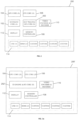
- Fig. 1 shows an electronic chip according to one embodiment of the present disclosure.
- the electronic chip may include a single or a plurality of hardwired game engines that may be physically incorporated on the chip, which may, therefore, represent a system on chip (SOC).
- SOC system on chip
- the chip 100 may comprise a plurality of processing cores, each implementing in hardware a (hardwired) game engine 102, a graphics processing unit (GPU) 104, and a central processing unit (CPU) 106. Even though each core is shown as implementing in hardware a dedicated component, it is to be understood that a plurality of processing cores may implement one component or that one processing core may implement a plurality of components, such as the game engine 102, the GPU 104, and the CPU 106, in any combination.
- the chip 100 may comprise a plurality of game engines, a plurality of GPUs and a plurality of CPUs, in any number and combination.
- the chip 100 may be included in a host system (not shown) as a SOC.
- the hardwired game engine 102 can directly process specifically constructed data sets located either in an external main memory of the host system, which may be accessible via one or more ports of an on-chip memory controller 108 and/or which may be located in a specifically designated memory area (not shown) on the chip 100 itself.
- the hardwired game engine 102 may be able to determine, for instance, but not limited to, how objects cast shadows over other objects of a computer graphics scene, how objects are reflected in other objects or how the light falling on one object illuminates other surrounding objects. However, it is to be understood that the game engine 102 may be configured to perform other tasks and/or may provide other functionality, such as management, simulation and rendering of the objects of the computer graphics scene.
- the hardwired game engine 102 may have the GPU 104 on the chip 100 to its disposal.
- the hardwired game engine 102 can generate data sets specifically designated to be handled over to the GPU 104 on the chip 100.
- the hardwired game engine 102 can place these data sets in the external memory of the chip 100 via one or more ports of the on-chip memory controller 108 and/or place the data sets in a specifically designated memory area on the chip 100 itself.
- the hardwired game engine 102 may have means to command the GPU 104 on the chip 100 to process the data sets generated by the hardwired game engine 102, such as one or more of buffers, command channels and/or registers, either via a direct connection to the GPU 104 and/or indirectly via a connection to the CPU 106 on the chip 100. In the latter case, the CPU 106 on the chip 100 may be configured to instruct the GPU 104 to operate on the data sets generated by the hardwired game engine 102.
- the chip 100 may comprise a further video encoder and decoder 110, a display 112, and a hardware interface 114.
- the video encoder and decoder 110 may perform various dedicated functionality directed at encoding and decoding of video sequences.
- the display 112 may either be a display configured to display at least some of the output of the GPU 104 or may be configured to display a state of the chip 100, by, for example, using a plurality of status indicators.
- the display 112 may also be configured as an interface to provide data to an external display (not shown).
- the hardware interface 114 may comprise or represent one or more interfaces, which may be configured to provide data for individual components of the chip 100, such as the game engine 102, the GPU 104, the CPU 106, the video encoder and decoder 110, and/or to output data generated by the individual components, such as data generated by the game engine 102, the GPU 104 or the CPU 106.
- the hardware interface may be configured to comply with one or more standards, such as USB, HDMI and the like.
- Fig. 2 shows another embodiment of a chip according to the present disclosure.
- the chip 200 may be similar to the chip 100 of Fig. 1 . Therefore, the same reference signs as used in Fig. 1 have been used in Fig. 2 .
- the chip 200 may comprise one or more of a game engine 102, a GPU 104, a CPU 106, a memory controller 108, a video encoder and decoder 110, a display 112, and a hardware interface 114.
- the chip 200 may also comprise a plurality of game engines 102, a plurality of GPUs 104, and a plurality of CPUs 106, in any combination, which may be implemented in hardware by at least one or respective processing core of the chip 200.
- the single or the plurality of hardwired game engines 102 may be physically incorporated on the chip 200 to thereby form a SOC.
- the single or the plurality of hardwired game engines 102 may be incorporated on the SOC together with a single or a plurality of ray trace engines 202.
- the one or more ray trace engines 202 may be implemented by at least one processing core of the chip 200 and may be configured in such a way that the functionality of the one or more game engines 102 is augmented. As will be acknowledged by those skilled in the art, the typical functionality of a ray trace engine is known.
- the functionality may, for example, include viewport culling and coverage (z)-buffer culling to determine visibility of objects; voxelization of a scene as a preparation step for global illumination calculation; sparse voxel-based cone tracing for global illumination; muscle fiber mechanics and musculoskeletal skinning, finite element methods for biomechanical muscle modelling; fluid dynamics using SPH (smoothed-particle hydrodynamics) for realistic effects involving water volumes, volcanic lava volumes, and astrophysical effects related to, for example, surfaces of stars; real-time Eulerian water simulation; and/or realistic vegetation dynamics, in any combination.
- z viewport culling and coverage
- the one or more ray trace engines 202 may be used to augment the functionality of the hardwired game engine 102.
- the hardwired game engines 102 may transparently offload processing tasks to the ray trace engines 202. It is to be understood that the one or more ray trace engines 202 may perform certain tasks better and/or faster due to their specialization for given time restrictions.
- the ray trace engines 202 may be assigned to individual game engines 102 according to a workload of the game engines 102 or according to a predefined assignment. The assignment may be controlled by the game engines 102 or by the CPU 106 in accordance with internal conditions or responsive to commands received via the hardware interface 114 to the chip 200.
- Fig. 2a shows yet another embodiment of a chip according to the present disclosure, wherein each hardwired game engine may incorporate its own specialized ray trace engine.
- the chip 200' may include the same or similar parts as disclosed with regard to chips 100 and 200 in Figs. 1 and 2 . Therefore, the same reference signs have been used to denote similar parts.
- the chip 200' may include one or more GPUs 104, one or more CPUs 106, a memory controller 108, a video encoder and decoder 110, a display 112 and a hardware interface 114, in any combination.
- the individual components may be implemented by at least one processing core of the chip 200'.
- Chip 200' further includes a combined game engine 202' having an incorporated specialized version of a ray trace engine.
- the specialized version of the ray trace engine may be specifically optimized for the requirements of the functionality of the hardwired game engine 202'.
- the ray trace engine may be hardwired with the game engine to thereby optimize the data exchange, in terms of bandwidth and latency, between the game engine and the ray trace engine using internal communication buffers or by directly transmitting data from the game engine to the integrated ray trace engine.
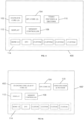
- Fig. 3 shows a game engine processor including a chip according to one embodiment of the present disclosure.
- the game engine processor 300 may include components similar to the components of chips 100, 200, and 200' as shown in Fig. 1 , Fig. 2, and Fig. 2a . Hence, same or similar parts have been denoted using the same reference signs.
- the game engine processor 300 may include one or more game engines 102, one or more ray trace cores 202, a memory controller 108, a video encoder and decoder 110, a display 112, and a hardware interface 114.
- the processor 300 may be realized in hardware as a game engine processor chip or a game engine processor package, where the package may contain a single or a plurality of integrated circuits implementing in hardware the functionality of the individual components.
- the hardwired game engine 102 may be incorporated into a hardware component, such as processor 300 that may be a stand-alone game engine processor chip or a game engine processor package.
- the game engine processor may be particularly useful in the case of high end 3D graphics or gaming computers. These computer systems typically contain separate host CPUs together with separate 3D graphics cards with one or more GPUs.
- the stand-alone game engine processor 300 could, for instance, be placed in a 3D graphics card together with one or more GPUs, but is not so limited.
- the game engine processor 300 may include additional means to communicate data sets related to the functionality of the hardwired game engine 102 to and from external GPUs, for example, by using the GPUs on-chip DMA (Direct Memory Access) facilities, which may allow access to and from the GPU's video memory.
- the additional means may be implemented using the hardware interface 114 or using another communication controller (not shown).
- Fig. 4 shows a graphics processor including a chip or chip assembly according to one embodiment of the present disclosure.
- the graphics processor 400 may include similar components as discussed with regard to Figs. 1 to 3 . Hence, same or similar components have been denoted using the same reference signs.
- the graphics processor 400 may include at least one of one or more game engines 102, one or more GPUs 104, a memory controller 108, a video encoder and decoder 110, a display 112, and a hardware interface 114, in any combination.
- the one or more hardwired game engines 102 may also be physically incorporated together with one or more ray trace engines (not shown) configured to augment the game engine functionality in the graphics processor 400.
- the graphics processor 400 may be embodied as a stand-alone "discrete" graphics processor chip or a stand-alone discrete graphics processor package, where the package may contain one or more integrated circuits.
- Fig. 4a shows another embodiment of a graphics processor including a chip or chip assembly according to the present disclosure.
- the graphics processor 400' may include the same or like components as the graphics processor 400 of Fig. 4 . Therefore, the same reference signs have been used to denote the same or like components.
- the graphics processor 400' may include one or more GPUs 104, a memory controller 108, a video encoder and decoder 110, a display 112, and a hardware interface 114, in any combination.
- the graphics processor 400' may include a plurality of hardwired game engines 402 that may be physically incorporated in the graphics processor 400', wherein each hardwired game engine 402 incorporates its own specialized ray trace engine optimized to augment the functionality of the game engine.
- the hardwired game engine 402 may be similar to the game engine 202' as shown in Fig. 2a .
- one or more hardware game engines 102, 402 may be incorporated into a stand-alone discrete graphics processor chip or package, where the graphics processor chip or package may include one or more integrated circuits.
- Multiple integrated circuits in a package could be, for instance, connected to each other with the use of an interposer and/or by stacking and/or by using a similar fabrication process as discussed in detail above.
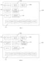
- Figs. 5, 5a , and 5b disclose embodiments of chips according to the present disclosure.
- the chips 500, 500' and 500" may include components similar to the components as shown in Figs. 1 to 4 . Hence, same reference signs have been used in Figs. 5, 5a , and 5b .
- Chip 500 of Fig. 5 may include one or more game engines 102, one or more GPUs 104, a memory controller 108, a video encoder and decoder 110, a display 112, and a hardware interface 114, in any combination. As discussed with regard to Figs. 1 and 2 , individual components may be implemented by at least one processing core of the chip 500.
- the chip 500 may further include a plurality of CPUs 106a, 106b, where each CPU may be configured to execute instructions according to a different instruction set architecture (ISA).
- ISA instruction set architecture
- the hardwired game engine 102 and said multiple types of CPUs 106a, 106b may be incorporated into a single hardware device, such as a SOC.
- the chip 500 may be able to run software compiled for different platforms, systems or architecture, for instance, but not limited to systems based on Intel's x86 architecture as commonly used in personal computers and systems based on the ARM instruction set, which may be typically used in mobile phones and tablets, by directing respective instructions to either CPU 106a and/or to CPU 106b.
- the chip 500 may include logic to determine, for each program code to be executed on the chip 500, an architecture for which the program code was compiled and to assign the program code to a respective CPU.
- Fig. 5 shows only two types of CPUs 106a, 106b, it is to be understood that other types of CPUs 106a, 106b for execution of instructions according to other ISAs can be used without departing from the scope of the present disclosure.
- chip 500' may include the same or similar components as discussed above with regard to chip 500, which are denoted in Fig. 5a using the same reference signs. Similar to chip 200 shown in Fig. 2 , chip 500' may further include one or more ray trace engines 502. The one or more of hardwired game engines 102 may be physically incorporated on a SOC, together with the one or more ray trace engines 202 configured in such a way that the functionality of the hardwired game engines 102 is augmented. The chip 500' may incorporate multiple types of CPUs where each type of CPU is designed to execute a different ISA.
- Chip 500" as shown in Fig. 5b may include the same or similar components as chips 500 and 500' discussed above with regard to Figs. 5 and 5a . Therefore, the same reference signs have been used in Fig. 5b .
- Chip 500" may include one or more game engines 502' similar to the game engines 202' as discussed above with regard to Fig. 2a and the game engines 402 as discussed above with regard to Fig. 4a .
- the chip 502' may include the one or more hardwired game engines 502' physically incorporated on a SOC, where each hardwired game engine 502' may incorporate its own specialized ray trace engine optimized to augment the functionality of the respective game engine 502'.
- the chip 502' may incorporate multiple types of CPUs where each type of CPU may be designed to execute instructions according to a different ISA.
- Fig. 6 shows a system according to one embodiment of the present disclosure.
- the system 600 may include a CPU 602 together with a game engine coprocessor 604.
- the game engine coprocessor 604 may comprise one or more chips as discussed above with regard to Figs. 1 to 5 .
- the game engine coprocessor 604 may incorporate one or more hardwired game engines 606 and, optionally, one or more ray trace engines 608.
- the optional ray trace engines 608 may be configured in such a way that the functionality of the game engine 606 may be augmented.
- the game engine coprocessor 604 may further comprise a memory controller 610 and a hardware interface 612 to communicate with the CPU 602.
- the CPU 602 may include one or more CPU cores 614, a memory controller 616, and a hardware interface 618.
- the game engine coprocessor 604 can be understood as a separate chip, optionally with its own package, which may be connected to the CPU 602 via an interface bus, such as a PCI express bus, or any other bus interface or interconnect.
- the game engine coprocessor 604 may contain its own memory controller 610 where the memory may be located outside the game engine coprocessor 604 or on the game engine coprocessor 604.
- the system 600 may further include one or more GPUs (not shown) and may comprise interfaces to connect to the one or more GPUs, for example, the PCI express bus.
- the PCI express bus may be any other interconnect or bus technology could be used to interconnect the CPU 602 with the game engine coprocessor 604 and the one or more GPUs.
- the CPU 602 may issue commands to the game engine coprocessor 604, which may then prepare data sets and commands that can be communicated back to the CPU 602 or, via the interfaces 602, 618 to an external discrete GPU.
- a higher performance can be reached by offloading CPU tasks to the game engine coprocessor 604 which may contain circuits specifically designed for these tasks.
- the one or more tasks may include one or more of determining how objects cast shadows over other objects, determining how objects are reflected in other objects, or determining how the light falling on one object illuminates other surrounding objects, and the like. It is to be understood that this enumeration is not limited and can be extended by one or more other tasks as defined above.
- the dedicated memory controller 610 on the game engine coprocessor 604 may allow the game engine coprocessor 604 to use its local memory to perform specific game engine tasks. This may advantageously improve performance by increasing I/O speed and bandwidth.
- Fig. 6a shows a chip 700 according to one embodiment of the present disclosure.
- the chip 700 may include a CPU 702 with a single or a plurality of CPU cores.
- the chip 700 may further include one or more hardwired game engines 704 and optionally, one or more ray trace engines 706 that may be configured in such a way that the functionality of the game engine 704 is augmented.
- chip 700 may be regarded as a variation of system 600 as discussed above with regard to Fig. 6 .
- chip 700 may integrate the system on a single chip or in a chip assembly.
- the chip 700 may further include a memory controller 708 and an interface 710.
- the chip 700 may be a single chip containing both the CPU 702 and the hardwired game engine 702 with the optional ray trace cores 706 on a single chip, where the memory controller 708 can be shared by both the CPU 702 and the game engines 704 to interface with external components, such as external GPUs.
- the interface 710 may be used to interface with one or more external discrete GPUs (not shown), via an interconnect or bus, such as the PCI express bus or any other type of bus or interconnect.
- Figs. 7a, 7b, and 7c show various examples of chip assemblies according to embodiments of the present disclosure. It is to be understood that a chip according to one embodiment of the present disclosure can be divided into multiple sub-chips and provided with required interconnections between the sub-chips, such as thousands or tens of thousands of interconnections, in such a way that the chip assembly functions in the same way as a single chip would function. Notwithstanding that embodiments of the present disclosure relate to the game engine on a chip, the chip may also be implemented as a chip assembly. Both a single chip as well as an implementation as a chip assembly, such as the chip assembly shown in Figs. 7a, 7b, and 7c are, therefore, to be understood as a game engine on a chip according to embodiments of the present disclosure.
- Figs. 7a, 7b and 7c show exemplary chip assemblies according to one or more embodiments of the present disclosure.
- the chip assemblies may include a package substrate 800, a plurality of sub-chips 802, and an interposer 804.
- the chip assembly may be configured on the package substrate 800 via the interposer 804.
- the plurality of sub-chips 802 may together constitute the game engine according to the embodiments of the present disclosure and the plurality of sub-chips 802 may be interconnected via the interposer 804.
- the interposer 804 may itself be a large silicon die with metal interconnect layers that may be produced with chip production equipment.
- the metal interconnect layers on the interposer 804 may replace the interconnection layers that otherwise would interconnect various areas of a single chip.
- the interposer 804 can be connected to the package substrate 800 using through-silicon-vias 806.
- Fig. 7b shows yet another embodiment of a chip assembly using another method of interconnecting the plurality of sub-chips 802 into a single game engine.
- the various sub-chips 802 may be integrated into the chip assembly using micro-bridges 808 that may be embedded in the package substrate 800.
- the micro-bridges 808 may be themselves silicon dies with metal interconnect layers produced by chip production equipment.
- the metal interconnect layers on the micro-bridges 808 may replace the interconnection layers that otherwise would interconnect various areas of a single chip.
- Fig. 7c shows yet another example embodiment of a chip assembly.
- the plurality of sub-chips 802 may be interconnected vertically into the chip assembly, placed on the package substrate 800. This may also be referred to as 3D chip stacking.
- Interconnecting sub-chips 802 vertically may use, for example, though-silicon-vias, such as the through-silicon-vias 806 of Fig. 7a , or use inductive coupling technology to enable near field wireless communication between 3D stacked chips.
Landscapes
- Engineering & Computer Science (AREA)
- Theoretical Computer Science (AREA)
- Physics & Mathematics (AREA)
- General Physics & Mathematics (AREA)
- Computer Hardware Design (AREA)
- Computer Graphics (AREA)
- Multimedia (AREA)
- Computing Systems (AREA)
- General Engineering & Computer Science (AREA)
- Image Generation (AREA)
- Information Transfer Systems (AREA)
- Multi Processors (AREA)
Claims (15)
- Puce électronique (200, 300, 500', 600, 700) comprenant :un premier noyau de traitement qui met en oeuvre un moteur de jeu (102, 606) au sein d'un matériel par des circuits électroniques dédiés ; etun deuxième noyau de traitement qui met en oeuvre un moteur de traçage de rayons (202, 502, 608) au sein d'un matériel par des circuits électroniques dédiés ;une interface matérielle (114, 612, 614, 710) qui couple le moteur de jeu (102, 606) mis en oeuvre dans le premier noyau de traitement au moteur de traçage de rayons (202, 502, 608) mis en oeuvre dans le deuxième noyau de traitement, dans laquelle l'interface matérielle (114, 612, 614, 710) couple directement le moteur de jeu (102, 606) et le moteur de traçage de rayons (202, 502, 608) ou couple le moteur de jeu (102, 606) et le moteur de traçage de rayons (202, 502, 608) à l'aide de mémoires tampon ;dans laquelle le moteur de jeu (102, 606) est configuré pour décharger un ensemble de tâches ou de sous-tâches du moteur de jeu (102, 606) vers le moteur de traçage de rayons (202, 502, 608) via l'interface matérielle (114, 612, 614, 710).
- Puce (200, 300, 500', 600, 700) selon la revendication 1, dans laquelle la puce (200, 300, 500', 600, 700) comprend en outre une pluralité de noyaux de traitement, chacun des noyaux de traitement mettant en oeuvre un moteur de jeu (102, 606) au sein d'un matériel par des circuits électroniques dédiés ou un moteur de traçage de rayons (202, 502, 608) au sein d'un matériel par des circuits électroniques dédiés, dans laquelle chacun de la pluralité de moteurs de jeu (102, 606) est associé à l'un de la pluralité de moteurs de traçage de rayons (202, 502, 608).
- Puce (200, 300, 500', 600, 700) selon la revendication 1 ou 2, comprenant en outre un noyau de traitement qui met en oeuvre une unité centrale de traitement (106, 106a, 106b, 602, 702).
- Puce (200, 300, 500', 600, 700) selon l'une des revendications 1 ou 2, comprenant en outre une pluralité de noyaux de traitement qui mettent en oeuvre une pluralité d'unités centrales de traitement (106, 106a, 106b, 602, 702), chaque unité centrale de traitement (106, 106a, 106b, 602, 702) étant configurée pour exécuter les instructions d'une architecture d'instructions différente.
- Puce (200, 300, 500', 600, 700) selon l'une des revendications précédentes, dans laquelle le moteur de jeu (102, 606) est configuré pour communiquer des données via l'interface matérielle (114, 612, 614, 710) avec une unité de traitement graphique (104).
- Puce (200, 300, 500', 600, 700) selon la revendication 5, dans laquelle la puce (200, 300, 500', 600, 700) comprend l'unité de traitement graphique (104).
- Puce (200, 300, 500', 600, 700) selon l'une des revendications 1 à 6, dans laquelle au moins l'un des noyaux de traitement met en oeuvre une unité de traitement graphique (104), la puce (200, 300, 500', 600, 700) comprenant en outre une mémoire, dans laquelle le moteur de jeu (102, 606) est configuré pour générer des données pour l'unité de traitement graphique (104) et pour fournir les données à l'unité de traitement graphique (104) via la mémoire, ou dans laquelle l'unité de traitement graphique (104) comprend une mémoire vidéo et le moteur de jeu (102, 606) est configuré pour fournir des données à l'unité de traitement graphique (104) via la mémoire vidéo.
- Puce (200, 300, 500', 600, 700) selon l'une des revendications 1 à 7, dans laquelle le moteur de jeu (102, 606) est configuré pour exécuter une ou plusieurs tâche(s) afin de générer des commandes et/ou des ensembles de données, dans laquelle le moteur de jeu (102, 606) et le moteur de traçage de rayons (202, 502, 608) sont couplés afin d'exécuter la ou les tâche(s), et dans laquelle la ou les tâche(s) comprend/comprennent un ou plusieurs de la détermination de la manière dont des objets produisent des ombres sur d'autres objets, de la détermination de la manière dont des objets sont réfléchis dans d'autres objets, et de la détermination dont une lumière qui atteint un objet éclaire d'autres objets environnants.
- Puce (200, 300, 500', 600, 700) selon l'une des revendications 1 à 8, la puce (200, 300, 500', 600, 700) étant un système (600) sur puce (200, 300, 500', 600, 700).
- Ensemble de puce comprenant :
au moins une puce (200, 300, 500', 600, 700) selon l'une des revendications 1 à 9. - Ensemble de puce selon la revendication 10, comprenant en outre une ou plusieurs d'au moins une unité centrale de traitement (106, 106a, 106b, 602, 702), dans lequel la au moins une unité centrale de traitement (106, 106a, 106b, 602, 702) est reliée à la au moins une interface matérielle (114, 612, 614, 710) de la puce (200, 300, 500', 600, 700), au moins une unité de traitement graphique (104), dans lequel la au moins une unité de traitement graphique (104) est reliée à la au moins une interface matérielle (114, 612, 614, 710) de la puce (200, 300, 500', 600, 700), et un contrôleur de mémoire (108, 610, 708) configuré pour échanger des données avec le moteur de jeu (102, 606) de la puce (200, 300, 500', 600, 700).
- Ensemble de puce selon la revendication 10, comprenant en outre une pluralité de circuits intégrés empilés, dans lequel un circuit intégré est empilé par-dessus un autre circuit intégré ou par-dessus une autre puce.
- Kit comprenant l'ensemble de puce selon l'une quelconque des revendications 10 à 12, dans lequel le kit est un boîtier-système ou un boîtier sur boîtier.
- Dispositif informatique comprenant :au moins une puce (200, 300, 500', 600, 700) selon l'une des revendications 1 à 9 ; etun écran (112) configuré pour afficher des données sur la base des données fournies par la au moins une puce (200, 300, 500', 600, 700).
- Dispositif informatique selon la revendication 14, dans lequel le dispositif informatique est un dispositif mobile, un smartphone ou un dispositif de réalité virtuelle.
Priority Applications (1)
| Application Number | Priority Date | Filing Date | Title |
|---|---|---|---|
| EP24153184.7A EP4332906A3 (fr) | 2015-09-16 | 2016-09-16 | Moteur de jeu sur puce |
Applications Claiming Priority (4)
| Application Number | Priority Date | Filing Date | Title |
|---|---|---|---|
| US201562219593P | 2015-09-16 | 2015-09-16 | |
| US201562220167P | 2015-09-17 | 2015-09-17 | |
| US15/047,556 US11295506B2 (en) | 2015-09-16 | 2016-02-18 | Chip with game engine and ray trace engine |
| PCT/EP2016/072018 WO2017046354A1 (fr) | 2015-09-16 | 2016-09-16 | Moteur de jeu sur une puce |
Related Child Applications (1)
| Application Number | Title | Priority Date | Filing Date |
|---|---|---|---|
| EP24153184.7A Division EP4332906A3 (fr) | 2015-09-16 | 2016-09-16 | Moteur de jeu sur puce |
Publications (2)
| Publication Number | Publication Date |
|---|---|
| EP3349870A1 EP3349870A1 (fr) | 2018-07-25 |
| EP3349870B1 true EP3349870B1 (fr) | 2024-01-24 |
Family
ID=58238830
Family Applications (2)
| Application Number | Title | Priority Date | Filing Date |
|---|---|---|---|
| EP16775106.4A Active EP3349870B1 (fr) | 2015-09-16 | 2016-09-16 | Moteur de jeu sur une puce |
| EP24153184.7A Pending EP4332906A3 (fr) | 2015-09-16 | 2016-09-16 | Moteur de jeu sur puce |
Family Applications After (1)
| Application Number | Title | Priority Date | Filing Date |
|---|---|---|---|
| EP24153184.7A Pending EP4332906A3 (fr) | 2015-09-16 | 2016-09-16 | Moteur de jeu sur puce |
Country Status (6)
| Country | Link |
|---|---|
| US (4) | US11295506B2 (fr) |
| EP (2) | EP3349870B1 (fr) |
| CN (1) | CN108025210A (fr) |
| DK (1) | DK3349870T3 (fr) |
| ES (1) | ES2977462T3 (fr) |
| WO (1) | WO2017046354A1 (fr) |
Families Citing this family (9)
| Publication number | Priority date | Publication date | Assignee | Title |
|---|---|---|---|---|
| CN107930118B (zh) * | 2017-12-28 | 2021-04-13 | 苏州蜗牛数字科技股份有限公司 | 一种Unity引擎后处理效果过程可视化方法和装置 |
| US11301951B2 (en) | 2018-03-15 | 2022-04-12 | The Calany Holding S. À R.L. | Game engine and artificial intelligence engine on a chip |
| CN109324816A (zh) * | 2018-09-12 | 2019-02-12 | Oppo广东移动通信有限公司 | 游戏加载方法及相关产品 |
| US10909652B2 (en) | 2019-03-15 | 2021-02-02 | Intel Corporation | Enabling product SKUs based on chiplet configurations |
| US11625884B2 (en) * | 2019-06-18 | 2023-04-11 | The Calany Holding S. À R.L. | Systems, methods and apparatus for implementing tracked data communications on a chip |
| US11579688B2 (en) * | 2019-06-28 | 2023-02-14 | Canon Kabushiki Kaisha | Imaging display device and wearable device |
| WO2021031110A1 (fr) * | 2019-08-20 | 2021-02-25 | 深圳市大疆创新科技有限公司 | Procédé et dispositif de génération de fichier de configuration et support d'enregistrement |
| CN120127083A (zh) * | 2020-02-28 | 2025-06-10 | 华为技术有限公司 | 一种芯片架构及相关方法 |
| JP2023011071A (ja) * | 2021-07-11 | 2023-01-23 | 株式会社スクウェア・エニックス | プラン処理プログラムおよびプラン処理システム |
Citations (4)
| Publication number | Priority date | Publication date | Assignee | Title |
|---|---|---|---|---|
| US20060106591A1 (en) * | 2004-11-16 | 2006-05-18 | Bordes Jean P | System with PPU/GPU architecture |
| KR20100003518A (ko) * | 2008-07-01 | 2010-01-11 | 주식회사 아이리버 | 게임기용 mpu 및 3d 그래픽 프로세서 |
| US20110242427A1 (en) * | 2010-04-01 | 2011-10-06 | Timothy Ramsdale | Method and System for Providing 1080P Video With 32-Bit Mobile DDR Memory |
| US20160117152A1 (en) * | 2014-02-06 | 2016-04-28 | Oxide Interactive, LLC | Method and system of a command buffer between a cpu and gpu |
Family Cites Families (49)
| Publication number | Priority date | Publication date | Assignee | Title |
|---|---|---|---|---|
| EP0430501B1 (fr) * | 1989-11-17 | 1999-02-03 | Digital Equipment Corporation | Système et méthode pour dessiner des polygones non corrompus |
| US5835693A (en) * | 1994-07-22 | 1998-11-10 | Lynch; James D. | Interactive system for simulation and display of multi-body systems in three dimensions |
| US6348919B1 (en) * | 1995-12-18 | 2002-02-19 | 3Dlabs Inc, Ltd. | Graphics system with optimized use of unified local and frame buffers |
| US6570564B1 (en) * | 1999-09-24 | 2003-05-27 | Sun Microsystems, Inc. | Method and apparatus for rapid processing of scene-based programs |
| US6816750B1 (en) * | 2000-06-09 | 2004-11-09 | Cirrus Logic, Inc. | System-on-a-chip |
| US7079133B2 (en) * | 2000-11-16 | 2006-07-18 | S3 Graphics Co., Ltd. | Superscalar 3D graphics engine |
| US6961055B2 (en) * | 2001-05-09 | 2005-11-01 | Free Radical Design Limited | Methods and apparatus for constructing virtual environments |
| US20050086040A1 (en) * | 2003-10-02 | 2005-04-21 | Curtis Davis | System incorporating physics processing unit |
| US7812844B2 (en) | 2004-01-28 | 2010-10-12 | Lucid Information Technology, Ltd. | PC-based computing system employing a silicon chip having a routing unit and a control unit for parallelizing multiple GPU-driven pipeline cores according to the object division mode of parallel operation during the running of a graphics application |
| US7053901B2 (en) * | 2003-12-11 | 2006-05-30 | Nvidia Corporation | System and method for accelerating a special purpose processor |
| US20050215319A1 (en) * | 2004-03-23 | 2005-09-29 | Harmonix Music Systems, Inc. | Method and apparatus for controlling a three-dimensional character in a three-dimensional gaming environment |
| US8747226B2 (en) * | 2004-07-07 | 2014-06-10 | Nintendo Of America, Inc. | Car-based entertainment system with video gaming |
| US7609884B1 (en) * | 2004-12-23 | 2009-10-27 | Pme Ip Australia Pty Ltd | Mutual information based registration of 3D-image volumes on GPU using novel accelerated methods of histogram computation |
| KR100632535B1 (ko) | 2004-12-29 | 2006-10-11 | 엘지전자 주식회사 | 이동통신단말기용 삼차원 그래픽 엔진 및 그래픽 제공 방법 |
| CN1298049C (zh) * | 2005-03-08 | 2007-01-31 | 北京中星微电子有限公司 | 一种图形引擎芯片及其应用方法 |
| US8317618B2 (en) * | 2005-12-15 | 2012-11-27 | At&T Intellectual Property I, Lp | System, method and computer program for enabling an interactive game |
| US7697751B2 (en) * | 2005-12-29 | 2010-04-13 | Graphics Properties Holdings, Inc. | Use of ray tracing for generating images for auto-stereo displays |
| FR2896895B1 (fr) * | 2006-02-01 | 2008-09-26 | Redway Soc Par Actions Simplifiee | Procede de synthese d'une image virtuelle par lancer de faisceaux |
| US8028290B2 (en) | 2006-08-30 | 2011-09-27 | International Business Machines Corporation | Multiple-core processor supporting multiple instruction set architectures |
| US9811935B2 (en) * | 2007-04-26 | 2017-11-07 | Ford Global Technologies, Llc | Emotive advisory system and method |
| US9329052B2 (en) | 2007-08-07 | 2016-05-03 | Qualcomm Incorporated | Displaying image data and geographic element data |
| WO2009097612A1 (fr) * | 2008-01-31 | 2009-08-06 | The Johns Hopkins University | Analyse d'image automatisée pour imagerie par résonance magnétique |
| US8257173B2 (en) | 2008-02-05 | 2012-09-04 | Disney Enterprises, Inc. | System and method for driving artificial intelligence (AI) characters having continuous reevaluation of current goals and navigation path |
| US8390618B2 (en) * | 2008-03-03 | 2013-03-05 | Intel Corporation | Technique for improving ray tracing performance |
| US8200594B1 (en) | 2008-09-10 | 2012-06-12 | Nvidia Corporation | System, method, and computer program product for accelerating a game artificial intelligence process |
| US9275487B1 (en) * | 2009-04-08 | 2016-03-01 | Pixar Animation Studios | System and method for performing non-affine deformations |
| KR101004110B1 (ko) * | 2009-05-28 | 2010-12-27 | 주식회사 실리콘아츠 | 레이 트레이싱 코어 및 이를 포함하는 레이 트레이싱 칩 |
| US8996337B1 (en) * | 2009-07-10 | 2015-03-31 | Nvidia Corporation | Hierarchical position-based dynamics |
| KR101706094B1 (ko) | 2010-01-14 | 2017-02-14 | 삼성전자주식회사 | 로봇용 관절 구동장치 및 이를 포함하는 로봇, 로봇용 관절 구동장치의 케이블 연결방법 |
| US8522254B2 (en) * | 2010-06-25 | 2013-08-27 | International Business Machines Corporation | Programmable integrated processor blocks |
| US10237563B2 (en) | 2012-12-11 | 2019-03-19 | Nvidia Corporation | System and method for controlling video encoding using content information |
| US20140168236A1 (en) * | 2012-12-19 | 2014-06-19 | Qnx Software Systems Limited | Gpu display adjustments |
| US9811775B2 (en) | 2012-12-24 | 2017-11-07 | Google Inc. | Parallelizing neural networks during training |
| US20150106673A1 (en) * | 2013-10-16 | 2015-04-16 | Taiwan Semiconductor Manufacturing Company Ltd. | Method and apparatus for on-the-fly memory channel built-in-self-test |
| US9327199B2 (en) * | 2014-03-07 | 2016-05-03 | Microsoft Technology Licensing, Llc | Multi-tenancy for cloud gaming servers |
| KR102207562B1 (ko) * | 2014-03-10 | 2021-01-27 | 에스케이하이닉스 주식회사 | 다양한 경로로 신호 입력이 가능한 적층 반도체 장치 및 반도체 시스템 |
| KR102244619B1 (ko) * | 2014-09-30 | 2021-04-26 | 삼성전자 주식회사 | 가속 구조를 생성 및 탐색하는 방법 |
| US20170243403A1 (en) | 2014-11-11 | 2017-08-24 | Bent Image Lab, Llc | Real-time shared augmented reality experience |
| KR102370617B1 (ko) * | 2015-04-23 | 2022-03-04 | 삼성전자주식회사 | 적응적 샘플링을 수행하여 영상을 처리하는 방법 및 장치. |
| US9880005B2 (en) | 2015-07-09 | 2018-01-30 | Invensense, Inc. | Method and system for providing a plurality of navigation solutions |
| US11244225B2 (en) | 2015-07-10 | 2022-02-08 | Samsung Electronics Co., Ltd. | Neural network processor configurable using macro instructions |
| US9443192B1 (en) | 2015-08-30 | 2016-09-13 | Jasmin Cosic | Universal artificial intelligence engine for autonomous computing devices and software applications |
| WO2017086922A1 (fr) | 2015-11-17 | 2017-05-26 | Intel IP Corporation | Dispositifs et procédés de suivi de faisceau pour bandes de hautes fréquences 5g |
| US10817802B2 (en) | 2016-05-07 | 2020-10-27 | Intel Corporation | Apparatus for hardware accelerated machine learning |
| TW201812646A (zh) | 2016-07-18 | 2018-04-01 | 美商南坦奧美克公司 | 分散式機器學習系統、分散式機器學習方法、以及產生代用資料之方法 |
| US10486060B2 (en) | 2016-11-23 | 2019-11-26 | Microsoft Technology Licensing, Llc | Tracking core for providing input to peripherals in mixed reality environments |
| US11256977B2 (en) | 2017-12-29 | 2022-02-22 | Facebook, Inc. | Lowering hardware for neural networks |
| US20190236606A1 (en) | 2018-01-31 | 2019-08-01 | Salesforce.Com, Inc. | Systems, methods, and apparatuses for implementing a virtual chain model for distributed ledger technologies in a cloud based computing environment |
| US11301951B2 (en) | 2018-03-15 | 2022-04-12 | The Calany Holding S. À R.L. | Game engine and artificial intelligence engine on a chip |
-
2016
- 2016-02-18 US US15/047,556 patent/US11295506B2/en active Active
- 2016-09-16 EP EP16775106.4A patent/EP3349870B1/fr active Active
- 2016-09-16 ES ES16775106T patent/ES2977462T3/es active Active
- 2016-09-16 WO PCT/EP2016/072018 patent/WO2017046354A1/fr not_active Ceased
- 2016-09-16 CN CN201680053259.XA patent/CN108025210A/zh active Pending
- 2016-09-16 EP EP24153184.7A patent/EP4332906A3/fr active Pending
- 2016-09-16 DK DK16775106.4T patent/DK3349870T3/da active
-
2022
- 2022-03-14 US US17/694,254 patent/US11663769B2/en active Active
-
2023
- 2023-05-12 US US18/196,649 patent/US12249018B2/en active Active
-
2025
- 2025-02-13 US US19/053,265 patent/US20250182372A1/en active Pending
Patent Citations (4)
| Publication number | Priority date | Publication date | Assignee | Title |
|---|---|---|---|---|
| US20060106591A1 (en) * | 2004-11-16 | 2006-05-18 | Bordes Jean P | System with PPU/GPU architecture |
| KR20100003518A (ko) * | 2008-07-01 | 2010-01-11 | 주식회사 아이리버 | 게임기용 mpu 및 3d 그래픽 프로세서 |
| US20110242427A1 (en) * | 2010-04-01 | 2011-10-06 | Timothy Ramsdale | Method and System for Providing 1080P Video With 32-Bit Mobile DDR Memory |
| US20160117152A1 (en) * | 2014-02-06 | 2016-04-28 | Oxide Interactive, LLC | Method and system of a command buffer between a cpu and gpu |
Also Published As
| Publication number | Publication date |
|---|---|
| WO2017046354A1 (fr) | 2017-03-23 |
| US20220198736A1 (en) | 2022-06-23 |
| US11295506B2 (en) | 2022-04-05 |
| US20230281908A1 (en) | 2023-09-07 |
| US20250182372A1 (en) | 2025-06-05 |
| CN108025210A (zh) | 2018-05-11 |
| EP4332906A3 (fr) | 2024-05-15 |
| EP4332906A2 (fr) | 2024-03-06 |
| US12249018B2 (en) | 2025-03-11 |
| ES2977462T3 (es) | 2024-08-23 |
| US20170075858A1 (en) | 2017-03-16 |
| DK3349870T3 (da) | 2024-04-22 |
| US11663769B2 (en) | 2023-05-30 |
| EP3349870A1 (fr) | 2018-07-25 |
Similar Documents
| Publication | Publication Date | Title |
|---|---|---|
| US12249018B2 (en) | Game engine on a chip | |
| US10089264B2 (en) | Callback interrupt handling for multi-threaded applications in computing environments | |
| CN113253979A (zh) | 用于云游戏的系统架构 | |
| US10776156B2 (en) | Thread priority mechanism | |
| US10430189B2 (en) | GPU register allocation mechanism | |
| TWI894167B (zh) | 用以促進封裝經壓縮資料的設備和方法,及用以促進資料解壓縮的設備和方法 | |
| CN109564676B (zh) | 管芯上曲面细分分配 | |
| CN112334878A (zh) | 用于虚拟化显示器的装置和方法 | |
| CN113094298A (zh) | 对共享本地存储器进行分区的机制 | |
| CN108694697B (zh) | 从模板印刷缓冲器控制粗糙像素大小 | |
| WO2017201676A1 (fr) | Mécanisme de fenêtre auto-adaptatif | |
| WO2018004860A1 (fr) | Architecture de tramage entrelacé et d'ombrage de pixels destinée à des systèmes de réalité virtuelle et de vues multiples | |
| US20170169537A1 (en) | Accelerated touch processing in computing environments | |
| US20260079879A1 (en) | Non-homogeneous chiplets | |
| DE102019123443A1 (de) | Mechanismus zum gemeinsamen Benutzen von Registern | |
| DE102019124705A1 (de) | Multiphasenarchitektur für Mehrraten-Pixelschattierung | |
| CN109844802B (zh) | 用于在图形处理器中提高线程并行性的机制 | |
| US12400618B2 (en) | Avoiding flicker in association with hotplug of a display | |
| US20200104166A1 (en) | Microcontroller-based flexible thread scheduling launching in computing environments | |
| US12361628B2 (en) | Configurable multiple-die graphics processing unit | |
| EP3734454A1 (fr) | Mécanisme de sonnette virtuelle mappé en mémoire | |
| CN122057233A (en) | On-chip game engine | |
| CN118537201A (zh) | 具有优化的可变速率着色的多gpu多显示器分片渲染 | |
| CN118212342A (zh) | 用于低等待时间渲染的内容感知的注视点asw |
Legal Events
| Date | Code | Title | Description |
|---|---|---|---|
| STAA | Information on the status of an ep patent application or granted ep patent |
Free format text: STATUS: THE INTERNATIONAL PUBLICATION HAS BEEN MADE |
|
| PUAI | Public reference made under article 153(3) epc to a published international application that has entered the european phase |
Free format text: ORIGINAL CODE: 0009012 |
|
| STAA | Information on the status of an ep patent application or granted ep patent |
Free format text: STATUS: REQUEST FOR EXAMINATION WAS MADE |
|
| 17P | Request for examination filed |
Effective date: 20180329 |
|
| AK | Designated contracting states |
Kind code of ref document: A1 Designated state(s): AL AT BE BG CH CY CZ DE DK EE ES FI FR GB GR HR HU IE IS IT LI LT LU LV MC MK MT NL NO PL PT RO RS SE SI SK SM TR |
|
| AX | Request for extension of the european patent |
Extension state: BA ME |
|
| DAV | Request for validation of the european patent (deleted) | ||
| DAX | Request for extension of the european patent (deleted) | ||
| STAA | Information on the status of an ep patent application or granted ep patent |
Free format text: STATUS: EXAMINATION IS IN PROGRESS |
|
| 17Q | First examination report despatched |
Effective date: 20211104 |
|
| GRAP | Despatch of communication of intention to grant a patent |
Free format text: ORIGINAL CODE: EPIDOSNIGR1 |
|
| STAA | Information on the status of an ep patent application or granted ep patent |
Free format text: STATUS: GRANT OF PATENT IS INTENDED |
|
| INTG | Intention to grant announced |
Effective date: 20230822 |
|
| GRAS | Grant fee paid |
Free format text: ORIGINAL CODE: EPIDOSNIGR3 |
|
| RAP3 | Party data changed (applicant data changed or rights of an application transferred) |
Owner name: TMRW FOUNDATION IP SARL |
|
| GRAA | (expected) grant |
Free format text: ORIGINAL CODE: 0009210 |
|
| STAA | Information on the status of an ep patent application or granted ep patent |
Free format text: STATUS: THE PATENT HAS BEEN GRANTED |
|
| AK | Designated contracting states |
Kind code of ref document: B1 Designated state(s): AL AT BE BG CH CY CZ DE DK EE ES FI FR GB GR HR HU IE IS IT LI LT LU LV MC MK MT NL NO PL PT RO RS SE SI SK SM TR |
|
| REG | Reference to a national code |
Ref country code: GB Ref legal event code: FG4D |
|
| REG | Reference to a national code |
Ref country code: CH Ref legal event code: EP |
|
| REG | Reference to a national code |
Ref country code: DE Ref legal event code: R096 Ref document number: 602016085481 Country of ref document: DE |
|
| REG | Reference to a national code |
Ref country code: IE Ref legal event code: FG4D |
|
| P01 | Opt-out of the competence of the unified patent court (upc) registered |
Effective date: 20240219 |
|
| REG | Reference to a national code |
Ref country code: DK Ref legal event code: T3 Effective date: 20240418 |
|
| REG | Reference to a national code |
Ref country code: LT Ref legal event code: MG9D |
|
| REG | Reference to a national code |
Ref country code: NL Ref legal event code: FP |
|
| PG25 | Lapsed in a contracting state [announced via postgrant information from national office to epo] |
Ref country code: IS Free format text: LAPSE BECAUSE OF FAILURE TO SUBMIT A TRANSLATION OF THE DESCRIPTION OR TO PAY THE FEE WITHIN THE PRESCRIBED TIME-LIMIT Effective date: 20240524 |
|
| PG25 | Lapsed in a contracting state [announced via postgrant information from national office to epo] |
Ref country code: LT Free format text: LAPSE BECAUSE OF FAILURE TO SUBMIT A TRANSLATION OF THE DESCRIPTION OR TO PAY THE FEE WITHIN THE PRESCRIBED TIME-LIMIT Effective date: 20240124 |
|
| PG25 | Lapsed in a contracting state [announced via postgrant information from national office to epo] |
Ref country code: GR Free format text: LAPSE BECAUSE OF FAILURE TO SUBMIT A TRANSLATION OF THE DESCRIPTION OR TO PAY THE FEE WITHIN THE PRESCRIBED TIME-LIMIT Effective date: 20240425 |
|
| REG | Reference to a national code |
Ref country code: AT Ref legal event code: MK05 Ref document number: 1651731 Country of ref document: AT Kind code of ref document: T Effective date: 20240124 |
|
| PG25 | Lapsed in a contracting state [announced via postgrant information from national office to epo] |
Ref country code: RS Free format text: LAPSE BECAUSE OF FAILURE TO SUBMIT A TRANSLATION OF THE DESCRIPTION OR TO PAY THE FEE WITHIN THE PRESCRIBED TIME-LIMIT Effective date: 20240424 Ref country code: HR Free format text: LAPSE BECAUSE OF FAILURE TO SUBMIT A TRANSLATION OF THE DESCRIPTION OR TO PAY THE FEE WITHIN THE PRESCRIBED TIME-LIMIT Effective date: 20240124 |
|
| PG25 | Lapsed in a contracting state [announced via postgrant information from national office to epo] |
Ref country code: AT Free format text: LAPSE BECAUSE OF FAILURE TO SUBMIT A TRANSLATION OF THE DESCRIPTION OR TO PAY THE FEE WITHIN THE PRESCRIBED TIME-LIMIT Effective date: 20240124 |
|
| PG25 | Lapsed in a contracting state [announced via postgrant information from national office to epo] |
Ref country code: RS Free format text: LAPSE BECAUSE OF FAILURE TO SUBMIT A TRANSLATION OF THE DESCRIPTION OR TO PAY THE FEE WITHIN THE PRESCRIBED TIME-LIMIT Effective date: 20240424 Ref country code: NO Free format text: LAPSE BECAUSE OF FAILURE TO SUBMIT A TRANSLATION OF THE DESCRIPTION OR TO PAY THE FEE WITHIN THE PRESCRIBED TIME-LIMIT Effective date: 20240424 Ref country code: LT Free format text: LAPSE BECAUSE OF FAILURE TO SUBMIT A TRANSLATION OF THE DESCRIPTION OR TO PAY THE FEE WITHIN THE PRESCRIBED TIME-LIMIT Effective date: 20240124 Ref country code: IS Free format text: LAPSE BECAUSE OF FAILURE TO SUBMIT A TRANSLATION OF THE DESCRIPTION OR TO PAY THE FEE WITHIN THE PRESCRIBED TIME-LIMIT Effective date: 20240524 Ref country code: HR Free format text: LAPSE BECAUSE OF FAILURE TO SUBMIT A TRANSLATION OF THE DESCRIPTION OR TO PAY THE FEE WITHIN THE PRESCRIBED TIME-LIMIT Effective date: 20240124 Ref country code: GR Free format text: LAPSE BECAUSE OF FAILURE TO SUBMIT A TRANSLATION OF THE DESCRIPTION OR TO PAY THE FEE WITHIN THE PRESCRIBED TIME-LIMIT Effective date: 20240425 Ref country code: FI Free format text: LAPSE BECAUSE OF FAILURE TO SUBMIT A TRANSLATION OF THE DESCRIPTION OR TO PAY THE FEE WITHIN THE PRESCRIBED TIME-LIMIT Effective date: 20240124 Ref country code: BG Free format text: LAPSE BECAUSE OF FAILURE TO SUBMIT A TRANSLATION OF THE DESCRIPTION OR TO PAY THE FEE WITHIN THE PRESCRIBED TIME-LIMIT Effective date: 20240124 Ref country code: AT Free format text: LAPSE BECAUSE OF FAILURE TO SUBMIT A TRANSLATION OF THE DESCRIPTION OR TO PAY THE FEE WITHIN THE PRESCRIBED TIME-LIMIT Effective date: 20240124 |
|
| PG25 | Lapsed in a contracting state [announced via postgrant information from national office to epo] |
Ref country code: PL Free format text: LAPSE BECAUSE OF FAILURE TO SUBMIT A TRANSLATION OF THE DESCRIPTION OR TO PAY THE FEE WITHIN THE PRESCRIBED TIME-LIMIT Effective date: 20240124 Ref country code: PT Free format text: LAPSE BECAUSE OF FAILURE TO SUBMIT A TRANSLATION OF THE DESCRIPTION OR TO PAY THE FEE WITHIN THE PRESCRIBED TIME-LIMIT Effective date: 20240524 |
|
| REG | Reference to a national code |
Ref country code: ES Ref legal event code: FG2A Ref document number: 2977462 Country of ref document: ES Kind code of ref document: T3 Effective date: 20240823 |
|
| PG25 | Lapsed in a contracting state [announced via postgrant information from national office to epo] |
Ref country code: SE Free format text: LAPSE BECAUSE OF FAILURE TO SUBMIT A TRANSLATION OF THE DESCRIPTION OR TO PAY THE FEE WITHIN THE PRESCRIBED TIME-LIMIT Effective date: 20240124 Ref country code: PT Free format text: LAPSE BECAUSE OF FAILURE TO SUBMIT A TRANSLATION OF THE DESCRIPTION OR TO PAY THE FEE WITHIN THE PRESCRIBED TIME-LIMIT Effective date: 20240524 Ref country code: PL Free format text: LAPSE BECAUSE OF FAILURE TO SUBMIT A TRANSLATION OF THE DESCRIPTION OR TO PAY THE FEE WITHIN THE PRESCRIBED TIME-LIMIT Effective date: 20240124 Ref country code: LV Free format text: LAPSE BECAUSE OF FAILURE TO SUBMIT A TRANSLATION OF THE DESCRIPTION OR TO PAY THE FEE WITHIN THE PRESCRIBED TIME-LIMIT Effective date: 20240124 |
|
| PG25 | Lapsed in a contracting state [announced via postgrant information from national office to epo] |
Ref country code: SM Free format text: LAPSE BECAUSE OF FAILURE TO SUBMIT A TRANSLATION OF THE DESCRIPTION OR TO PAY THE FEE WITHIN THE PRESCRIBED TIME-LIMIT Effective date: 20240124 |
|
| PG25 | Lapsed in a contracting state [announced via postgrant information from national office to epo] |
Ref country code: CZ Free format text: LAPSE BECAUSE OF FAILURE TO SUBMIT A TRANSLATION OF THE DESCRIPTION OR TO PAY THE FEE WITHIN THE PRESCRIBED TIME-LIMIT Effective date: 20240124 Ref country code: EE Free format text: LAPSE BECAUSE OF FAILURE TO SUBMIT A TRANSLATION OF THE DESCRIPTION OR TO PAY THE FEE WITHIN THE PRESCRIBED TIME-LIMIT Effective date: 20240124 |
|
| REG | Reference to a national code |
Ref country code: DE Ref legal event code: R097 Ref document number: 602016085481 Country of ref document: DE |
|
| PG25 | Lapsed in a contracting state [announced via postgrant information from national office to epo] |
Ref country code: SK Free format text: LAPSE BECAUSE OF FAILURE TO SUBMIT A TRANSLATION OF THE DESCRIPTION OR TO PAY THE FEE WITHIN THE PRESCRIBED TIME-LIMIT Effective date: 20240124 |
|
| PG25 | Lapsed in a contracting state [announced via postgrant information from national office to epo] |
Ref country code: SM Free format text: LAPSE BECAUSE OF FAILURE TO SUBMIT A TRANSLATION OF THE DESCRIPTION OR TO PAY THE FEE WITHIN THE PRESCRIBED TIME-LIMIT Effective date: 20240124 Ref country code: SK Free format text: LAPSE BECAUSE OF FAILURE TO SUBMIT A TRANSLATION OF THE DESCRIPTION OR TO PAY THE FEE WITHIN THE PRESCRIBED TIME-LIMIT Effective date: 20240124 Ref country code: RO Free format text: LAPSE BECAUSE OF FAILURE TO SUBMIT A TRANSLATION OF THE DESCRIPTION OR TO PAY THE FEE WITHIN THE PRESCRIBED TIME-LIMIT Effective date: 20240124 Ref country code: EE Free format text: LAPSE BECAUSE OF FAILURE TO SUBMIT A TRANSLATION OF THE DESCRIPTION OR TO PAY THE FEE WITHIN THE PRESCRIBED TIME-LIMIT Effective date: 20240124 Ref country code: CZ Free format text: LAPSE BECAUSE OF FAILURE TO SUBMIT A TRANSLATION OF THE DESCRIPTION OR TO PAY THE FEE WITHIN THE PRESCRIBED TIME-LIMIT Effective date: 20240124 |
|
| PLBE | No opposition filed within time limit |
Free format text: ORIGINAL CODE: 0009261 |
|
| STAA | Information on the status of an ep patent application or granted ep patent |
Free format text: STATUS: NO OPPOSITION FILED WITHIN TIME LIMIT |
|
| PG25 | Lapsed in a contracting state [announced via postgrant information from national office to epo] |
Ref country code: IT Free format text: LAPSE BECAUSE OF FAILURE TO SUBMIT A TRANSLATION OF THE DESCRIPTION OR TO PAY THE FEE WITHIN THE PRESCRIBED TIME-LIMIT Effective date: 20240124 |
|
| PG25 | Lapsed in a contracting state [announced via postgrant information from national office to epo] |
Ref country code: IT Free format text: LAPSE BECAUSE OF FAILURE TO SUBMIT A TRANSLATION OF THE DESCRIPTION OR TO PAY THE FEE WITHIN THE PRESCRIBED TIME-LIMIT Effective date: 20240124 |
|
| 26N | No opposition filed |
Effective date: 20241025 |
|
| PG25 | Lapsed in a contracting state [announced via postgrant information from national office to epo] |
Ref country code: SI Free format text: LAPSE BECAUSE OF FAILURE TO SUBMIT A TRANSLATION OF THE DESCRIPTION OR TO PAY THE FEE WITHIN THE PRESCRIBED TIME-LIMIT Effective date: 20240124 Ref country code: MC Free format text: LAPSE BECAUSE OF FAILURE TO SUBMIT A TRANSLATION OF THE DESCRIPTION OR TO PAY THE FEE WITHIN THE PRESCRIBED TIME-LIMIT Effective date: 20240124 |
|
| REG | Reference to a national code |
Ref country code: BE Ref legal event code: MM Effective date: 20240930 |
|
| PG25 | Lapsed in a contracting state [announced via postgrant information from national office to epo] |
Ref country code: BE Free format text: LAPSE BECAUSE OF NON-PAYMENT OF DUE FEES Effective date: 20240930 |
|
| REG | Reference to a national code |
Ref country code: CH Ref legal event code: U11 Free format text: ST27 STATUS EVENT CODE: U-0-0-U10-U11 (AS PROVIDED BY THE NATIONAL OFFICE) Effective date: 20251001 |
|
| PGFP | Annual fee paid to national office [announced via postgrant information from national office to epo] |
Ref country code: DK Payment date: 20250922 Year of fee payment: 10 Ref country code: DE Payment date: 20250919 Year of fee payment: 10 |
|
| PGFP | Annual fee paid to national office [announced via postgrant information from national office to epo] |
Ref country code: NL Payment date: 20250922 Year of fee payment: 10 Ref country code: TR Payment date: 20250910 Year of fee payment: 10 Ref country code: LU Payment date: 20250922 Year of fee payment: 10 |
|
| PGFP | Annual fee paid to national office [announced via postgrant information from national office to epo] |
Ref country code: GB Payment date: 20250923 Year of fee payment: 10 |
|
| PGFP | Annual fee paid to national office [announced via postgrant information from national office to epo] |
Ref country code: FR Payment date: 20250926 Year of fee payment: 10 |
|
| PGFP | Annual fee paid to national office [announced via postgrant information from national office to epo] |
Ref country code: IE Payment date: 20250919 Year of fee payment: 10 |
|
| PGFP | Annual fee paid to national office [announced via postgrant information from national office to epo] |
Ref country code: CH Payment date: 20251029 Year of fee payment: 10 |
|
| PG25 | Lapsed in a contracting state [announced via postgrant information from national office to epo] |
Ref country code: CY Free format text: LAPSE BECAUSE OF FAILURE TO SUBMIT A TRANSLATION OF THE DESCRIPTION OR TO PAY THE FEE WITHIN THE PRESCRIBED TIME-LIMIT; INVALID AB INITIO Effective date: 20160916 |
|
| PGFP | Annual fee paid to national office [announced via postgrant information from national office to epo] |
Ref country code: ES Payment date: 20251226 Year of fee payment: 10 |
|
| PG25 | Lapsed in a contracting state [announced via postgrant information from national office to epo] |
Ref country code: HU Free format text: LAPSE BECAUSE OF FAILURE TO SUBMIT A TRANSLATION OF THE DESCRIPTION OR TO PAY THE FEE WITHIN THE PRESCRIBED TIME-LIMIT; INVALID AB INITIO Effective date: 20160916 |