EP3350910B1 - Stromwandler zur begrenzung von schaltüberspannung - Google Patents
Stromwandler zur begrenzung von schaltüberspannung Download PDFInfo
- Publication number
- EP3350910B1 EP3350910B1 EP16845422.1A EP16845422A EP3350910B1 EP 3350910 B1 EP3350910 B1 EP 3350910B1 EP 16845422 A EP16845422 A EP 16845422A EP 3350910 B1 EP3350910 B1 EP 3350910B1
- Authority
- EP
- European Patent Office
- Prior art keywords
- electronic switch
- power electronic
- turn
- voltage
- inductance
- Prior art date
- Legal status (The legal status is an assumption and is not a legal conclusion. Google has not performed a legal analysis and makes no representation as to the accuracy of the status listed.)
- Active
Links
Images





Classifications
-
- H—ELECTRICITY
- H02—GENERATION; CONVERSION OR DISTRIBUTION OF ELECTRIC POWER
- H02M—APPARATUS FOR CONVERSION BETWEEN AC AND AC, BETWEEN AC AND DC, OR BETWEEN DC AND DC, AND FOR USE WITH MAINS OR SIMILAR POWER SUPPLY SYSTEMS; CONVERSION OF DC OR AC INPUT POWER INTO SURGE OUTPUT POWER; CONTROL OR REGULATION THEREOF
- H02M1/00—Details of apparatus for conversion
- H02M1/32—Means for protecting converters other than automatic disconnection
-
- H—ELECTRICITY
- H02—GENERATION; CONVERSION OR DISTRIBUTION OF ELECTRIC POWER
- H02M—APPARATUS FOR CONVERSION BETWEEN AC AND AC, BETWEEN AC AND DC, OR BETWEEN DC AND DC, AND FOR USE WITH MAINS OR SIMILAR POWER SUPPLY SYSTEMS; CONVERSION OF DC OR AC INPUT POWER INTO SURGE OUTPUT POWER; CONTROL OR REGULATION THEREOF
- H02M1/00—Details of apparatus for conversion
- H02M1/08—Circuits specially adapted for the generation of control voltages for semiconductor devices incorporated in static converters
-
- H—ELECTRICITY
- H02—GENERATION; CONVERSION OR DISTRIBUTION OF ELECTRIC POWER
- H02M—APPARATUS FOR CONVERSION BETWEEN AC AND AC, BETWEEN AC AND DC, OR BETWEEN DC AND DC, AND FOR USE WITH MAINS OR SIMILAR POWER SUPPLY SYSTEMS; CONVERSION OF DC OR AC INPUT POWER INTO SURGE OUTPUT POWER; CONTROL OR REGULATION THEREOF
- H02M1/00—Details of apparatus for conversion
- H02M1/32—Means for protecting converters other than automatic disconnection
- H02M1/34—Snubber circuits
- H02M1/344—Active dissipative snubbers
-
- H—ELECTRICITY
- H02—GENERATION; CONVERSION OR DISTRIBUTION OF ELECTRIC POWER
- H02M—APPARATUS FOR CONVERSION BETWEEN AC AND AC, BETWEEN AC AND DC, OR BETWEEN DC AND DC, AND FOR USE WITH MAINS OR SIMILAR POWER SUPPLY SYSTEMS; CONVERSION OF DC OR AC INPUT POWER INTO SURGE OUTPUT POWER; CONTROL OR REGULATION THEREOF
- H02M1/00—Details of apparatus for conversion
- H02M1/32—Means for protecting converters other than automatic disconnection
- H02M1/34—Snubber circuits
- H02M1/348—Passive dissipative snubbers
-
- H—ELECTRICITY
- H03—ELECTRONIC CIRCUITRY
- H03K—PULSE TECHNIQUE
- H03K17/00—Electronic switching or gating, i.e. not by contact-making and –breaking
- H03K17/08—Modifications for protecting switching circuit against overcurrent or overvoltage
- H03K17/081—Modifications for protecting switching circuit against overcurrent or overvoltage without feedback from the output circuit to the control circuit
- H03K17/0812—Modifications for protecting switching circuit against overcurrent or overvoltage without feedback from the output circuit to the control circuit by measures taken in the control circuit
- H03K17/08128—Modifications for protecting switching circuit against overcurrent or overvoltage without feedback from the output circuit to the control circuit by measures taken in the control circuit in composite switches
-
- H—ELECTRICITY
- H03—ELECTRONIC CIRCUITRY
- H03K—PULSE TECHNIQUE
- H03K17/00—Electronic switching or gating, i.e. not by contact-making and –breaking
- H03K17/08—Modifications for protecting switching circuit against overcurrent or overvoltage
- H03K17/082—Modifications for protecting switching circuit against overcurrent or overvoltage by feedback from the output to the control circuit
- H03K17/0828—Modifications for protecting switching circuit against overcurrent or overvoltage by feedback from the output to the control circuit in composite switches
-
- H—ELECTRICITY
- H02—GENERATION; CONVERSION OR DISTRIBUTION OF ELECTRIC POWER
- H02M—APPARATUS FOR CONVERSION BETWEEN AC AND AC, BETWEEN AC AND DC, OR BETWEEN DC AND DC, AND FOR USE WITH MAINS OR SIMILAR POWER SUPPLY SYSTEMS; CONVERSION OF DC OR AC INPUT POWER INTO SURGE OUTPUT POWER; CONTROL OR REGULATION THEREOF
- H02M1/00—Details of apparatus for conversion
- H02M1/0048—Circuits or arrangements for reducing losses
- H02M1/0054—Transistor switching losses
-
- H—ELECTRICITY
- H02—GENERATION; CONVERSION OR DISTRIBUTION OF ELECTRIC POWER
- H02M—APPARATUS FOR CONVERSION BETWEEN AC AND AC, BETWEEN AC AND DC, OR BETWEEN DC AND DC, AND FOR USE WITH MAINS OR SIMILAR POWER SUPPLY SYSTEMS; CONVERSION OF DC OR AC INPUT POWER INTO SURGE OUTPUT POWER; CONTROL OR REGULATION THEREOF
- H02M3/00—Conversion of DC power input into DC power output
- H02M3/02—Conversion of DC power input into DC power output without intermediate conversion into AC
- H02M3/04—Conversion of DC power input into DC power output without intermediate conversion into AC by static converters
- H02M3/10—Conversion of DC power input into DC power output without intermediate conversion into AC by static converters using discharge tubes with control electrode or semiconductor devices with control electrode
- H02M3/145—Conversion of DC power input into DC power output without intermediate conversion into AC by static converters using discharge tubes with control electrode or semiconductor devices with control electrode using devices of a triode or transistor type requiring continuous application of a control signal
- H02M3/155—Conversion of DC power input into DC power output without intermediate conversion into AC by static converters using discharge tubes with control electrode or semiconductor devices with control electrode using devices of a triode or transistor type requiring continuous application of a control signal using semiconductor devices only
- H02M3/156—Conversion of DC power input into DC power output without intermediate conversion into AC by static converters using discharge tubes with control electrode or semiconductor devices with control electrode using devices of a triode or transistor type requiring continuous application of a control signal using semiconductor devices only with automatic control of output voltage or current, e.g. switching regulators
- H02M3/158—Conversion of DC power input into DC power output without intermediate conversion into AC by static converters using discharge tubes with control electrode or semiconductor devices with control electrode using devices of a triode or transistor type requiring continuous application of a control signal using semiconductor devices only with automatic control of output voltage or current, e.g. switching regulators including plural semiconductor devices as final control devices for a single load
-
- H—ELECTRICITY
- H02—GENERATION; CONVERSION OR DISTRIBUTION OF ELECTRIC POWER
- H02M—APPARATUS FOR CONVERSION BETWEEN AC AND AC, BETWEEN AC AND DC, OR BETWEEN DC AND DC, AND FOR USE WITH MAINS OR SIMILAR POWER SUPPLY SYSTEMS; CONVERSION OF DC OR AC INPUT POWER INTO SURGE OUTPUT POWER; CONTROL OR REGULATION THEREOF
- H02M7/00—Conversion of AC power input into DC power output; Conversion of DC power input into AC power output
- H02M7/42—Conversion of DC power input into AC power output without possibility of reversal
- H02M7/44—Conversion of DC power input into AC power output without possibility of reversal by static converters
- H02M7/48—Conversion of DC power input into AC power output without possibility of reversal by static converters using discharge tubes with control electrode or semiconductor devices with control electrode
- H02M7/53—Conversion of DC power input into AC power output without possibility of reversal by static converters using discharge tubes with control electrode or semiconductor devices with control electrode using devices of a triode or transistor type requiring continuous application of a control signal
- H02M7/537—Conversion of DC power input into AC power output without possibility of reversal by static converters using discharge tubes with control electrode or semiconductor devices with control electrode using devices of a triode or transistor type requiring continuous application of a control signal using semiconductor devices only, e.g. single switched pulse inverters
- H02M7/5387—Conversion of DC power input into AC power output without possibility of reversal by static converters using discharge tubes with control electrode or semiconductor devices with control electrode using devices of a triode or transistor type requiring continuous application of a control signal using semiconductor devices only, e.g. single switched pulse inverters in a bridge configuration
-
- Y—GENERAL TAGGING OF NEW TECHNOLOGICAL DEVELOPMENTS; GENERAL TAGGING OF CROSS-SECTIONAL TECHNOLOGIES SPANNING OVER SEVERAL SECTIONS OF THE IPC; TECHNICAL SUBJECTS COVERED BY FORMER USPC CROSS-REFERENCE ART COLLECTIONS [XRACs] AND DIGESTS
- Y02—TECHNOLOGIES OR APPLICATIONS FOR MITIGATION OR ADAPTATION AGAINST CLIMATE CHANGE
- Y02B—CLIMATE CHANGE MITIGATION TECHNOLOGIES RELATED TO BUILDINGS, e.g. HOUSING, HOUSE APPLIANCES OR RELATED END-USER APPLICATIONS
- Y02B70/00—Technologies for an efficient end-user side electric power management and consumption
- Y02B70/10—Technologies improving the efficiency by using switched-mode power supplies [SMPS], i.e. efficient power electronics conversion e.g. power factor correction or reduction of losses in power supplies or efficient standby modes
Definitions
- the present disclosure relates to the field of power electronics. More specifically, the present disclosure relates to a power converter configured for limiting switching overvoltage
- Commutation cells are commonly used in electronic systems that require conversion of a voltage source, including both DC-DC converters and DC-AC converters, which are often called inverters. With the limited space allowed for power converter circuits, such as those used for example in electric and/or electric hybrid automotive applications, and given the high cost of the semi-conductors, the demand for integration of these commutation cells increases.
- a known way of reducing the space occupied by semiconductors in power converter circuits is to increase their efficiency to allow the size of the cooling surface to be reduced.
- Losses in power electronic switches present in conventional power converter circuits are mainly caused by two sources; conduction losses and switching losses.
- One way to reduce switching losses is generally by accelerating turn-on and turn-off of the power electronic switches.
- fast turn-off of the power electronic switches induces overvoltage in stray inductances of their highfrequency loop. It is thus often required to slow down turning off of the power electronic switches to protect them against overvoltage. This may seriously impact the overall efficiency of conventional power converter circuits.
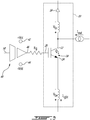
- FIG. 1 is an idealized circuit diagram of a conventional commutation cell such as those used in conventional power converter circuits.
- a commutation cell 10 converts a DC voltage V bus from a voltage source 12 (or from a capacitor) into a current source I out (or into an inductance) that usually generates a voltage V out appropriate for a load 14 connected to a positive tab of the voltage source 12, the load 14 being for example a resistive load, an electric motor, and the like.
- the commutation cell 10 comprises a freewheel diode 16 and a controlled power electronic switch 18, for example an isolated gate bipolar transistor (IGBT).
- IGBT isolated gate bipolar transistor
- a capacitor 20 ( C in ) is used to limit variations of the voltage V bus of the voltage source 12 and an inductance L out 32 is used to limit the variations of the output current I out .
- a gate driver (not shown in Figure 1 but shown on later Figures) controls turning on and off of the power electronic switch 18.
- Figure 1 illustrates a configuration of the commutation cell 10, of the load 14, and of the voltage source 12, in which energy flows from the voltage source 12 to the load 14, i.e. from left to right on the drawing.
- the commutation cell 10 can also be used in a reverse configuration in which energy flows in the opposite direction, in which case the load 14 is connected between the output inductance L out 32 and a negative tab of the voltage source 12.
- the power electronic switch 18 When turned on (i.e. closing), the power electronic switch 18 allows current to pass therethrough, from its collector 22 to its emitter 24; at that time, the power electronic switch 18 can be approximated as a closed circuit. When turned off (i.e. opening), the power electronic switch 18 does not allow current to pass therethrough and becomes an open circuit.
- the gate driver applies a variable control voltage between the gate 26 and the emitter 24 of the power electronic switch 18.
- the gate driver may act as a current source instead of as a voltage source.
- the voltage applied between the gate 26 and the emitter 24 is "high”
- the power electronic switch 18 allows passing of current from the collector 22 to the emitter 24.
- the voltage applied between the gate 26 and the emitter 24 is "low”
- the power electronic switch 18 blocks passage of current therethrough.
- a voltage difference between the gate 26 and the emitter 24, denoted V ge is controlled by the gate driver.
- V ge is greater than a threshold V ge(th) for the power electronic switch 18, the switch 18 is turned on and a voltage V ce between the collector 22 and the emitter 24 becomes near zero.
- V ge is lower than V ge(th) , the power electronic switch 18 is turned off and V ce eventually reaches V bus .
- Figure 2 is another circuit diagram of the conventional commutation cell of Figure 1 , showing parasitic (stray) inductances.
- connections between components of an actual commutation cell define parasitic inductances.
- the parasitic inductances are distributed at various places within the commutation cell 10
- a suitable model presented in Figure 2 shows two (2) distinct inductances representing the overall parasitic inductance, including an emitter inductance 30 of the power electronic switch 18 and an inductance 34 representative of all other parasitic inductances (other than the emitter inductance 30) around a high frequency loop 36 formed by the freewheel diode 16, the power electronic switch 18 and the capacitor 20.
- the high frequency loop 36 is a path where current changes significantly upon switching of the power electronic switch 18. It should be noted that an output inductance L out 32 is not part of the high frequency loop 36 because its current remains fairly constant through the commutation period.
- Figure 3 is a circuit diagram of a conventional commutation cell further showing a gate driver 40. Some elements of the commutation cell 10 are not shown on Figure 3 , in order to simplify the illustration.
- Figure 3 shows a gate driver 40 having a positive supply voltage 42, a negative supply voltage 44 and an output 46 being connected to the gate 26 of the power electronic switch 18 via a gate resistor R g .
- the positive supply voltage 42 of the gate driver 40 has a value denoted + V cc , for example +15 volts above a ground reference (shown on a later Figure) while the negative supply voltage 44 has value denoted -V dd , for example -5 volts below the ground reference.
- a ground reference of the gate driver 40 is connected to the emitter 24 of the power electronic switch 18; this connection is not shown on Figure 3 .
- An input 50 of the gate driver 40 is connected to a controller (not shown) of the commutation cell 10, as is well known in the art.
- a voltage at the output 46 of the gate driver 40 goes up to + V cc and goes down to - V dd in order to control the voltage at the gate 26.
- the input resistance of the gate 26 to emitter may be very high, especially in the case where the electronic switch 18 is an IGBT.
- a parasitic capacitance C ge (shown on a later Figure), present between the gate 26 and the emitter 24 and a parasitic Miller capacitance C gc (not shown), present between the gate 26 and the collector 22, for a total gate equivalent capacitor C ies , causes some current to flow from the output 46 when the gate driver 40 alternates between +V cc and -V dd .
- the value R g of the gate resistor is selected as a function of the parasitic capacitance C ies and of a desired switching rate of the power electronic switch 18 so that the voltage at the gate 26 changes at a rate appropriate for the desired switching rate.
- a current I igbt flowing through the power electronic switch 18 and through the emitter parasitic inductance 30 is essentially equal to I out when the power electronic switch 18 is closed, and quickly reduces to substantially zero when the power electronic switch 18 turns off.
- a voltage V Ls is induced across the parasitic inductance 34 and a voltage V Le is induced across the emitter parasitic inductance 30.
- the polarities shown across the inductances of the high frequency loop 36, including the emitter inductance 30, reflect voltages obtained upon turn-off of the power electronic switch 18, when the I igbt current diminishes very rapidly, di / dt thus taking a negative value.
- voltages across the inductances of the high frequency loop 36, including the emitter inductance 30 are in the opposite direction.
- V Ls and V Le are in series with V bus from the voltage source 12.
- V bus When the power electronic switch 18 turns off, the collector 22 to emitter 24 voltage increases until the freewheel diode 16 turns on. At that time, addition of V bus , V Ls and V Le results in an important overvoltage applied between the collector 22 and the emitter 24 of the power electronic switch 18.
- power electronic switches are rated for operation at some level of overvoltage, extreme overvoltage can reduce the lifetime of any power electronic switch to thereby lead to its premature failure.
- Figure 4 is a circuit diagram of an IGBT leg having resistive dividers connected across parasitic (stray) emitter inductances, forming compensation circuits.
- the circuit of Figure 4 was introduced in International Patent Publication No. WO 2014/161080 A1 to Jean-Marc Cyr et al., published on October 9, 2014 , the disclosure of which is incorporated by reference herein.
- Figure 4 shows a power converter having a pair of commutation cells connected in parallel, each commutation cell including a power electronic switch and a gate driver.
- the power converter may for example be an IGBT leg 90 including compensation circuits connected to gate drivers in a configuration that reduces overvoltage on the IGBTs.
- the IGBT leg 90 may for example form one third of a three-phase alternative current (AC) power source driving an electric motor (not shown) from battery 12.
- the IGBT leg 90 feeds a current source I out via an inductance L out through a phase tab (not shown) connected between top and bottom power electronic switches, the phase tab having a parasitic inductance L phase .
- Figure 4 introduces compensation circuits that optimize overvoltage on the IGBT using a resistive divider across the emitter parasitic inductance.
- the IGBT leg 90 comprises a top commutation cell including a top IGBT Q 2 and a bottom freewheel diode D 1 .
- the top IGBT Q 2 is driven by a gate driver 62 connected to a gate 64 of the top IGBT Q 2 via a resistor R4.
- a top compensation circuit includes a turn-on diode D 4 and resistors R 5 and R 6 .
- a bottom commutation cell includes a bottom IGBT Q 1 and a top freewheel diode D 2 .
- the bottom IGBT Q 1 is driven by a gate driver 60 connected to a gate 26 of the bottom IGBT Q 1 via a resistor R 1 .
- a bottom compensation circuit includes a turn-on diode D 3 and resistores R 2 and R 3 .
- the top commutation cell operates when I out is positive (in the direction shown in Figure 4 ) and the bottom commutation cell operates when I out is in the opposite direction.
- Components of the IGBT leg 90 are placed on a power module (not shown) having a positive voltage tab connected to +V bus , a negative voltage tab connected to -V bus (also not shown) and a phase voltage tab connected to L out . Connections between these components create a number of parasitic inductances, including a parasitic positive voltage tab L+ Vbus , a parasitic top collector inductance L c-high , a parasitic top emitter inductance L e-high , a parasitic bottom collector inductance L c-low , a parasitic bottom emitter inductance L e-low , a parasitic negative voltage tab inductance L -Vbus and input capacitor inductance L c .
- the two commutation cells combine with an input capacitance C in of a voltage source 12 to form a high frequency loop 92 of the IGBT leg 90.
- a ground reference 52 of the gate driver 60 (GND low) is connected to a bottom compensation circuit having a resistive divider circuit including the two resistors R 2 and R 3 and the turn-on diode D 3 , which allows the turn-on not to be impacted by the resistive divider by keeping the voltage at the emitter of the bottom IGBT Q 1 not lower than the ground reference 52.
- the turn-on diode D 3 is conducting while turning on the bottom IGBT Q 1 because the direction of its current in positive. In contrast, the turn-on diode D 3 is not conducting while turning off the bottom IGBT Q 1 because of the voltage induced across the emitter inductance during the di / dt applies a negative voltage across the turn-on diode D 3 .
- values of the resistors R 2 and R 3 are selected according to an acceptable overvoltage level allowed across the bottom IGBT Q 1 .
- a ratio of R 2 over R 3 is increased to reduce the overvoltage.
- the value of the equivalent gate resistor is set with these two resistors R 2 and R 3 in parallel, in series with a gate driver resistor R 1 .
- a value of the gate driver resistor R 1 is adjusted in a conventional manner according to a proper commutation behavior.
- the normal practice consisting in using a resistor R 1 in the ground connection of the gate driver to limit the current in the diodes that protect the gate driver 60 of the bottom IGBT Q 1 from a negative voltage when the top IGBT Q 2 turns off has been modified by splitting the resistor in two resistors, including R 1 in series with R 2 and R 3 connected in parallel, and by adapting their ratio to limit the effect of the emitter inductance on the di / dt.
- An equivalent resistor value may remain the same, but the voltage divider gives the desired weight of the emitter inductance to limit the overvoltage at the desired level.
- the overvoltage can be optimized as much as possible to reach the maximum IGBT rating while maintaining the speed of the di / dt for efficiency reasons. This is done by reducing a value of R 2 the resistor connected to the IGBT emitter, compared to R 3 the resistor connected to the power tab. The voltage across the emitter inductance is thus split in two parts and only the part of the voltage across R 2 is applied in the gate drive circuit to limit the gate voltage drop.
- the values of the resistors R 2 and R 3 are selected according to the level of overvoltage allowed across Q1.
- Figure 5 is a diagram showing turn-off waveforms of the bottom IGBT of Figure 4 .
- Figure 5 show the result of a resistive divider optimized for an operation at a bus voltage V bus of 500 Vdc.
- the ratio of R 2 over R 3 can be increased to reduce the overvoltage.
- the equivalent value of the two resistors R 2 and R 3 in parallel, is set in series with R 1 , which is adjusted according to the proper commutation behavior of the bottom IGBT Q 1 .
- the collector to emitter overvoltage may be optimized as much as possible to reach the maximum voltage rating of the bottom IGBT Q 1 . This is done by reducing a value of the resistor R 2 connected to the logical emitter of the bottom IGBT Q 1 compared to a value of the resistor R 3 connected to the power tab.
- the voltage across the emitter inductance L e-low alone or with the negative voltage tab inductance L- Vbus , is split in two parts and only the voltage across the resistor R 2 is applied at the reference 52 of the gate driver 60 to limit the voltage drop at the gate 26 of the bottom IGBT Q 1 .
- Figure 5 shows the current I igbt , the gate to emitter voltage V ge and the collector to emitter voltage V ce during turn-off of the bottom IGBT Q 1 of Figure 4 . It is notable that V ce peaks at a plateau 80 whose value is tailored according to the maximum voltage rating of the bottom IGBT Q 1 . This plateau 80 occurs while the rate of drop of V ge is contained at area 82 by the insertion of the voltage sample from the parasitic inductances L e-low and L -Vbus .
- Figure 6 is a circuit diagram in which the compensation circuits of Figure 4 are modified to impact the turn-on of the IGBTs.
- a variant of the circuit of Figure 6 was introduced in US Provisional Patent Application serial number 62/183,437 to Jean-Marc Cyr et al., filed on June 23, 2015 , the disclosure of which is incorporated by reference herein.
- Figure 6 shows a modified IGBT leg 95 in which the ground reference 52 (GND low) is now electrically connected to the emitter 24 of the bottom IGBT Q 1 via the turn-on diode D 3 placed in series with a resistor R D3 .
- the turn-on diode D 3 is polarized to become short when an emitter voltage of the bottom IGBT Q 1 is higher than a voltage of the ground reference 52.
- the ground reference 52 is also electrically connected across both parasitic inductances L e-low and L -Vbus via the resistor R 2 and R 3 .
- the resistor R 2 is placed in parallel with the series combination of the turn-on diode D 3 and of the resistor R D3 .
- resistor R D3 If the resistor R D3 is replaced by a short circuit, there is no compensation at turn-on and the IGBT leg 95 becomes equivalent to the IGBT leg 90, at least for the bottom compensation circuit.
- the turn-on diode D 3 selection of a proper value for the resistor R D3 allows to fine tune the turn-on of the bottom IGBT Q 1 independently from its turn-off, the bottom compensation circuit forming a resistive divider between R D3 in parallel with R 2 , this parallel combination being in series with R 3 .
- a ground reference 54 (GND high) is electrically connected to the emitter of the top IGBT Q 2 , via the turn-on diode D 4 placed in series with a resistor R D4 .
- Turn-on diode D 4 is polarized to become short when an emitter voltage of the top IGBT Q 2 is higher than a voltage of the ground reference 54.
- the ground reference 54 is also electrically connected to collector 22 of the bottom IGBT Q 1 via the resistor R 6 .
- the resistor R 5 is placed in parallel with the series combination of the turn-on diode D 4 and of the resistor R D4 .
- the top and bottom compensation circuits operate in similar ways.
- the emitter inductance L e-high of the top IGBT Q 2 is smaller than the emitter inductance L e-low of the bottom IGBT Q 1 .
- the emitter inductance L e-high is often too small to suitably clamp a voltage thereacross without increasing the gate resistor R 4 to protect the device.
- the emitter inductance L e-high of the top IGBT Q 2 in series with the collector inductance L c-low of the bottom IGBT Q 1 is oftentimes too low to be used to limit the overvoltage across the top IGBT Q 2 at the desired level.
- a power converter configured for limiting switching overvoltage.
- the power converter comprises a bottom commutation cell that includes a bottom power electronic switch having a bottom gate, a bottom gate driver and a bottom compensation circuit connected to a bottom parasitic inductance.
- the bottom compensation circuit applies a sample of a voltage induced across the bottom parasitic inductance to the bottom gate driver at turn-off of the bottom power electronic switch.
- the power converter also comprises a top commutation cell that includes top power electronic switch having a top gate, a top gate driver and a top compensation circuit connected to the bottom parasitic inductance.
- the top compensation circuit applies a sample of a voltage induced across the bottom parasitic inductance to the top gate driver at turn-off of the top power electronic switch.
- the top and bottom commutation cells are part of a loop, being connected at a junction of a collector of the bottom power electronic switch and of an emitter of the top power electronic switch.
- Various aspects of the present disclosure generally address one or more of the problems related to overvoltage occurring upon switching in a power converter.
- Circuits operable to limit overvoltage in commutation cells, especially at turn-off of IGBTs are described in international patent publications no WO 2013/082705 A1 , which belongs to the same family as US 2014/0321178 A1 , WO 2014/043795 A1 , WO 2014/161080 A1 , WO 2015/061901 A1 , WO 2015/070347 A1 and WO 2015/139132 A1 and in US provisional application no 62/183,437 , all of which are authored by Jean-Marc Cyr et al.
- the present technology provides control of overvoltage and switching losses at turn-off of a power electronic switch of a commutation cell. Circuits and methods presented herein are generally compatible with at least some aspects these other solutions to limit overvoltage at turn-off of power electronic switches.
- di / dt at turn-off of a power electronic switch induces a voltage across parasitic (stray) inductances of a high frequency loop of the commutation cell. This voltage is present across the power electronic switch in addition to a bus voltage providing power to the commutation cell. A sum of these voltages can exceed the maximum voltage rating of the power electronic switch. Solution described hereinabove are based on the application of a sample of the overvoltage present across parasitic inductances of the commutation cell to a gate driver of the power electronic switch.
- a parasitic inductance present in a "top" commutation cell may not be sufficient to provide a sufficient voltage sample to control the overvoltage present across the top power electronic switch.
- An improvement described in details hereinbelow comprises a compensation circuit that is configured to sample a voltage induced across a parasitic inductance of one commutation cell to control the overvoltage upon turn-off of the other commutation cell. According to this solution, voltage samples are taken in the commutation cell having the largest parasitic inductance and are applied at turn-off of both commutation cells.
- IGBT isolated gate bipolar transistors
- Commutation cell an assembly of electronic components connected to a voltage source that alternatively applies voltage from a voltage source and zero voltage to a current source connected to a load.
- Power converter circuit configured to convert energy from a first type of energy source, providing a different type of energy.
- Leg a combination of a pair of commutation cells forming a power converter.
- Overvoltage voltage across an electronic element that exceeds the voltage from the power source.
- Power electronic switch an active on and off switchable element of a commutation cell.
- top in the context of the present disclosure, the terms “top” and “bottom” do not relate to physical characteristics of any element of the power converter, but rather to their placement on circuits diagrams shown in the various drawings.
- Compensation circuit a circuit configured to provide a measure of the overvoltage on a power electronic switch as feedback to control and/or reduce the overvoltage.
- Parasitic inductance an inductance that is usually not formed of a discrete component, but rather formed by the connection of two or more components such as the connection between a power electronic switch and a circuit board; also called stray inductance.
- Voltage sample a voltage obtained from a circuit component, for example from a parasitic inductance, the obtained voltage being reduced by a voltage gain.
- Resistive gain adapter a combination of resistors providing a voltage gain.
- Turn-on diode a diode of a compensation circuit that is conductive during the turn-on of the power electronic switch in that compensation circuit.
- Turn-off diode a diode of a compensation circuit that is conductive during turn-off of the power electronic switch in that compensation circuit.
- Freewheel diode a diode in an anti-parallel position having regard to a power electronic switch.
- Gate driver a small buffer amplifier providing isolation and control signals for turning on and off a power electronic switch.
- Reference a floating ground reference of a gate driver on which a voltage sample can be applied.
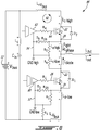
- FIG. 7 is a circuit diagram of an IGBT leg having turn-off diodes mounted in tandem according to an illustrative embodiment.
- IGBT leg 100 Several elements of an IGBT leg 100 were introduced in the foregoing description of Figures 4 and 5 and are not described in details hereinbelow.
- the same power electronic switches (IGBTs Q 1 and Q 2 ) and freewheel diodes ( D 1 and D 2 ) are placed on the same or similar circuit card, creating the same or equivalent parasitic inductances.
- the bottom commutation cell including the bottom IGBT Q 1 , the bottom gate driver 60 with its reference 52, and the bottom compensation circuit having the resistors R 2 , R 3 and R D3 , as well as the turn-on diode D 3 , is reproduced without significant changes.
- the bottom commutation cell of the IGBT leg 100 operates in the same manner as the bottom commutation cell of the IGBT leg 90 if the R D3 has zero resistance (being a short-circuit), or in the same manner as the bottom commutation cell of the IGBT leg 95 if a value of R D3 is greater than zero.
- the IGBT leg 100 mainly differs from the above-described circuits by its top compensation circuit that allows the top gate driver 62 to control the top IGBT Q 2 based on a sample of a voltage induced across the large bottom parasitic inductance L e-low and across the parasitic inductance L -Vbus .
- the IGBT leg 100 forms a power converter configured for limiting switching overvoltage.
- Top and bottom commutation cells form a loop, being connected at a junction of a collector 22 of a bottom power electronic switch, illustrated as the bottom IGBT Q 1 , and of an emitter 24 of a top power electronic switch, illustrated as the top IGBT Q 2 .
- the bottom commutation cell includes the bottom IGBT Q 1 , and a bottom compensation circuit connected to a bottom parasitic inductance that includes the parasitic emitter inductance L e-low of the bottom IGBT Q 1 and the parasitic negative voltage tab inductance L -Vbus .
- the bottom compensation circuit applies a sample of a voltage induced across the bottom parasitic inductance at turn-off of the bottom IGBT Q 1 .
- the top commutation cell includes the top IGBT Q 2 , and a top compensation circuit that is also connected to the bottom parasitic inductance.
- the top compensation circuit applies a sample of a voltage induced across the bottom parasitic emitter upon turn-off of the top IGBT Q 2 , when the opposite freewheel diode D 1 is conducting.
- Applying the sample of the voltage induced across the bottom parasitic inductance to the bottom gate driver 60 at turn-off of the bottom IGBT Q 1 controls the voltage induced across the bottom parasitic inductance. This in turn limits the overvoltage on the bottom IGBT Q 1 .
- applying the sample of the voltage induced across the bottom parasitic inductance to the top gate driver 62 at turn-off of the top IGBT Q 2 controls voltages induced throughout the parasitic inductance included in the loop of the IGBT leg 100. This in turn limits the overvoltage on the top IGBT Q 2 .
- the sample of the voltage induced across the bottom parasitic inductance upon turn-off of the bottom IGBT Q 1 is applied by the bottom compensation circuit to a reference 52 of a bottom gate driver 60 connected to a gate 26 of the bottom IGBT Q 1 .
- the sample of the voltage induced across the bottom parasitic inductance upon turn-off of the top IGBT Q 2 is applied by the top compensation circuit to a reference 54 of a top gate driver 62 connected to a gate 64 of the top IGBT Q 2 .
- the bottom compensation circuit comprises a bottom resistive gain adapter that includes resistors R 2 , R 3 and R D3 , as well as a turn-on diode D3 that places a resistor R D3 in parallel with R 2 when turning-on the bottom IGBT Q 1 .
- Values of the resistors R 2 , R 3 and R D3 may be similar to those of the circuits of Figures 4 and 6 , or may be selected according to the needs of a particular application.
- the resistor R 3 connects the reference 52 of the gate driver 60 downstream of the negative voltage tab. Connecting the resistor R 3 upstream of the negative voltage tab would exclude the parasitic negative voltage tab inductance L - Vbus . It is however generally desirable to connect the resistor R 3 downstream of the negative voltage tab in order to maximize the voltage to be sampled.
- the top compensation circuit includes a turn-off diode D 5 that connects the top compensation circuit to the bottom parasitic inductance upon di / dt at turn-off of the top IGBT Q 2 .
- the turn-off diode D 5 is selected such that a voltage drop across the turn-off diode D 5 is greater than a voltage drop across the bottom freewheel diode D 1 when D 1 is also conducting to ensure the load current will not circulate in the diode D 5 , which is a low power diode.
- the turn-off diode may include a pair of turn-off diodes D 5 connected in series to provide the desired voltage drop.
- the turn-off diode(s) D 5 upon turn-off of the top IGBT Q 2 , a large overvoltage induced between its collector 22 and its emitter 24 causes its emitter voltage to be more negative than a voltage of the negative voltage tab -V bus . D 5 therefore becomes conductive upon turn-off of the top IGBT Q 2 . In contrast, upon turn-on of the top IGBT Q 2 , its emitter voltage is higher than the voltage of the negative voltage tab -V bus and the turn-off diode D 5 is blocked.
- diode D 5 is shown connected to the capacitor C in , it could also be connected to GND low.
- the top compensation circuit comprises two resistive gain adapters formed of resistors R 5 , R 6 and R D4 , complemented with a turn-on diode D 4 .
- Values of the resistors R 5 , R 6 and R D4 may differ from to those of the circuits of Figures 4 and 6 .
- the top compensation circuit applies a sample of a voltage induced across a top parasitic inductance that includes the parasitic emitter inductance of the top power electronic switch L e-high and optionally includes the parasitic collector inductance L c-low of the bottom IGBT Q 1 .
- the turn-off diode D 5 and the resistor R 6 connect the reference 54 of the gate driver 62 downstream of the negative voltage tab.
- the resistor R 5 connects the reference 54 of the gate driver 62 directly on the collector 22 of the bottom IGBT Q 1 .
- Connecting the resistor R 5 to the phase tab of the IGBT leg 100 would exclude the parasitic collector inductance L c-low of the bottom IGBT Q 1 .
- a three-phase alternative current (AC) power source operable to drive a motor (not shown) or a similar load can be built by combining three (3) IGBT legs such as the IGBT leg 100.
- the description of the power converter configured for limiting switching overvoltage are illustrative only and are not intended to be in any way limiting. Other embodiments will readily suggest themselves to such persons with ordinary skill in the art having the benefit of the present disclosure. Furthermore, the power converter configured for limiting switching overvoltage may be customized to offer valuable solutions to existing needs and problems of overvoltage occurring upon switching in power converters.
- the power converter configured for limiting switching overvoltage is not limited in its application to the details of construction and parts illustrated in the accompanying drawings and described hereinabove.
- the proposed power converter configured for limiting switching overvoltage is capable of other embodiments and of being practiced in various ways. It is also to be understood that the phraseology or terminology used herein is for the purpose of description and not limitation.
Landscapes
- Engineering & Computer Science (AREA)
- Power Engineering (AREA)
- Power Conversion In General (AREA)
- Dc-Dc Converters (AREA)
Claims (13)
- Stromwandler (100), ausgelegt zur Begrenzung von Schaltüberspannung, umfassend:eine untere Kommutierungszelle, umfassend einen unteren Leistungselektronikschalter (Q1)und eine Freilaufdiode (D1), die parallel zu dem unteren Leistungselektronikschalter (Q1)geschaltet ist, wobei der untere Leistungselektronikschalter (Q1)ein unteres Gate, einen Treiber (60) des unteren Gates und eine untere Kompensationsschaltung aufweist, die mit der Emitterseite des unteren Leistungselektronikschalters (Q1)verbunden ist, um einen Abtastwert einer Spannung, die über die untere parasitäre Induktivität (Le-low) induziert wird, an den Treiber (60) des unteren Gates beim Ausschalten des unteren Leistungselektronikschalters (Q1) anzulegen; undeine obere Kommutierungszelle, die einen oberen Leistungselektronikschalter mit einem oberen Gate und einem Treiber für das obere Gate umfasst;wobei die obere und untere Kommutierungszelle Teil einer Schleife sind, verbunden an einer Verbindungsstelle (22) eines Kollektors des unteren Leistungselektronikschalters (Q1) und eines Emitters des oberen Leistungselektronikschalters (Q2),wobei die obere Kommutierungszelle ferner eine obere Kompensationsschaltung beinhaltet, verbunden mit der Emitterseite des unteren Leistungselektronikschalters (Q1), um einen Abtastwert einer Spannung, induziert über die untere parasitäre Induktivität (Le-low), an den Treiber (62) des oberen Gates beim Ausschalten des oberen Leistungselektronikschalters (Q2) anzulegen,wobei die obere Kompensationsschaltung eine Einschaltdiode (D4), eine Ausschaltdiode (D5) und zwei Widerstände (R5, R6) umfasst,wobei eine Massereferenz (54) über die Einschaltdiode (D4) elektrisch mit dem Emitter des oberen Leistungselektronikschalters (Q2) verbunden ist,wobei die Einschaltdiode (D4) dazu ausgelegt ist, polarisiert zu werden, um kurzgeschlossen zu werden, wenn eine Emitterspannung des oberen Leistungselektronikschalters (Q2) höher als eine Spannung der Massereferenz (54) ist, undwobei die Massereferenz (54) auch über einen der beiden Widerstände (R5, R6) mit einem Kollektor (22) des unteren Leistungselektronikschalters (Q1) elektrisch verbunden ist,wobei der Emitter des oberen Leistungselektronikschalters (Q2) über einen weiteren Widerstand (RD4) mit der Einschaltdiode (D4) elektrisch verbunden ist,und der andere der zwei Widerstände (R5, R6) die Massereferenz (54) mit der Abschaltdiode (D5) verbindet, wobei die Abschaltdiode (D5) mit der Emitterseite des unteren Leistungselektronikschalters (Q1) verbunden und so ausgewählt ist, dass ein Spannungsabfall an der Abschaltdiode (D5) größer ist als ein Spannungsabfall an der unteren Freilaufdiode (D1), die parallel zu dem unteren Leistungselektronikschalter (Q1) geschaltet ist.
- Stromwandler nach Anspruch 1, wobei die untere parasitäre Induktivität (Le-low) eine parasitäre Emitterinduktivität des unteren Leistungselektronikschalters (Q1) umfasst.
- Stromwandler nach Anspruch 1, wobei die untere parasitäre Induktivität (Le-low) eine parasitäre Emitterinduktivität des unteren Leistungselektronikschalters (Q1) und eine parasitäre Induktivität des negativen Spannungsanschlusses umfasst.
- Stromwandler nach einem der Ansprüche 1 oder 3, wobei das Anlegen des Abtastwerts der über die untere parasitäre Induktivität (Le-low) induzierten Spannung beim Ausschalten des unteren Leistungselektronikschalters (Q1) die über die untere parasitäre Induktivität (Le-low) induzierte Spannung regelt.
- Stromwandler nach Anspruch 1, wobei der Treiber (60) des unteren Gates einen unteren Referenzwert aufweist, um den Abtastwert der Spannung, die über die untere parasitäre Induktivität induziert wird, von der unteren Kompensationsschaltung zu empfangen.
- Stromwandler nach einem der Ansprüche 1 bis 5, wobei:
die untere Kompensationsschaltung dazu ausgelegt ist, den Abtastwert der Spannung, die über die untere parasitäre Induktivität (Le-low) induziert wird, an den Treiber (60) des unteren Gates beim Ausschalten des unteren Leistungselektronikschalters (Q1) unter Verwendung einer ersten Spannungsverstärkung anzulegen; und die untere Kompensationsschaltung dazu ausgelegt ist, einen weiteren Abtastwert der Spannung, die über die untere parasitäre Induktivität (Le-low) induziert wird, an den Treiber (60) des unteren Gates beim Einschalten des unteren Leistungselektronikschalters (Q1) unter Verwendung einer zweiten Spannungsverstärkung anzulegen, die niedriger als die erste Spannungsverstärkung und größer als oder gleich null ist. - Stromwandler nach Anspruch 6, wobei die untere Kompensationsschaltung einen unteren Widerstandsverstärkungsadapter mit einem ersten und einem zweiten Widerstand, die die erste Spannungsverstärkung definieren, und eine untere Einschaltdiode (D3) umfasst, dazu ausgelegt, einen dritten Widerstand parallel zu dem ersten Widerstand zu platzieren, wenn der untere Leistungselektronikschalter (Q1) eingeschaltet wird, wobei der erste, zweite und dritte Widerstand die zweite Spannungsverstärkung definieren.
- Stromwandler nach einem der Ansprüche 1 bis 7, wobei die Abschaltdiode (D5) zwei in Reihe geschaltete Abschaltdioden umfasst.
- Stromwandler nach einem der Ansprüche 1 bis 8, wobei die obere Kompensationsschaltung dazu ausgelegt ist, einen Abtastwert einer Spannung anzulegen, die über eine obere parasitäre Induktivität (Le-low) beim Einschalten des oberen Leistungselektronikschalters induziert wird.
- Stromwandler nach Anspruch 9, wobei die obere parasitäre Induktivität eine parasitäre Emitterinduktivität des oberen Leistungselektronikschalters ist.
- Stromwandler nach Anspruch 9, wobei die obere parasitäre Induktivität eine parasitäre Emitterinduktivität des oberen Leistungselektronikschalters (Q2) und eine parasitäre Kollektorinduktivität des unteren Leistungselektronikschalters (Q1) umfasst.
- Stromwandler nach einem der Ansprüche 1 bis 11, umfassend eine Eingangskapazität, wobei die Eingangskapazität die Schleife schließt, die mit der oberen und unteren Kommutierungszelle ausgebildet ist.
- Dreiphasige alternative Stromquelle, umfassend drei Instanzen des Stromwandlers nach einem der Ansprüche 1 bis 12.
Applications Claiming Priority (2)
| Application Number | Priority Date | Filing Date | Title |
|---|---|---|---|
| US201562218142P | 2015-09-14 | 2015-09-14 | |
| PCT/CA2016/051079 WO2017045071A1 (en) | 2015-09-14 | 2016-09-13 | Power converter configured for limiting switching overvoltage |
Publications (3)
| Publication Number | Publication Date |
|---|---|
| EP3350910A1 EP3350910A1 (de) | 2018-07-25 |
| EP3350910A4 EP3350910A4 (de) | 2019-05-08 |
| EP3350910B1 true EP3350910B1 (de) | 2021-04-14 |
Family
ID=58287983
Family Applications (1)
| Application Number | Title | Priority Date | Filing Date |
|---|---|---|---|
| EP16845422.1A Active EP3350910B1 (de) | 2015-09-14 | 2016-09-13 | Stromwandler zur begrenzung von schaltüberspannung |
Country Status (8)
| Country | Link |
|---|---|
| US (1) | US10468971B2 (de) |
| EP (1) | EP3350910B1 (de) |
| JP (1) | JP2018528753A (de) |
| KR (1) | KR20180052624A (de) |
| CN (1) | CN108141129B (de) |
| CA (1) | CA2997524A1 (de) |
| HK (1) | HK1258265A1 (de) |
| WO (1) | WO2017045071A1 (de) |
Families Citing this family (1)
| Publication number | Priority date | Publication date | Assignee | Title |
|---|---|---|---|---|
| WO2023001995A1 (fr) * | 2021-07-21 | 2023-01-26 | Valeo Systemes De Controle Moteur | Systeme de commutation et convertisseur de tension ou engin de mobilite comprenant un tel systeme de commutation |
Family Cites Families (21)
| Publication number | Priority date | Publication date | Assignee | Title |
|---|---|---|---|---|
| JPS61112421A (ja) * | 1984-11-06 | 1986-05-30 | Mitsubishi Electric Corp | バイポ−ラ・ダ−リントン・パワ−トランジスタの駆動回路 |
| US5723916A (en) * | 1996-05-17 | 1998-03-03 | Delco Electronics Corporation | Electrical load driving device including load current limiting circuitry |
| JP2000134908A (ja) * | 1998-10-27 | 2000-05-12 | Toshiba Corp | 電力変換装置 |
| KR100896139B1 (ko) * | 2001-08-13 | 2009-05-12 | 인덕토썸코오퍼레이션. | 고장 내성 전력 공급 장치 |
| JP3791400B2 (ja) * | 2001-11-22 | 2006-06-28 | 三菱電機株式会社 | 半導体装置 |
| US7940503B2 (en) * | 2008-05-27 | 2011-05-10 | Infineon Technologies Ag | Power semiconductor arrangement including conditional active clamping |
| CN101872967B (zh) * | 2009-04-24 | 2013-10-16 | 深圳市科陆变频器有限公司 | Igbt击穿保护电路 |
| KR101449083B1 (ko) * | 2010-05-06 | 2014-10-13 | 엘에스산전 주식회사 | 스위칭 게이트 드라이브 |
| JP5460519B2 (ja) * | 2010-08-09 | 2014-04-02 | 本田技研工業株式会社 | 半導体素子の駆動装置及び方法 |
| JP5746954B2 (ja) * | 2011-11-22 | 2015-07-08 | 株式会社 日立パワーデバイス | インバータ装置 |
| JP6239525B2 (ja) * | 2011-12-07 | 2017-11-29 | ティーエム4・インコーポレーテッド | Igbtのターンオフ過電圧の制限 |
| WO2013138219A1 (en) * | 2012-03-12 | 2013-09-19 | Board Of Trustees Of Michigan State University | High efficiency gate drive circuit for power transistors |
| WO2014043795A1 (en) | 2012-09-24 | 2014-03-27 | Tm4 Inc. | Topology for controlled power switch module |
| WO2014161080A1 (en) * | 2013-04-04 | 2014-10-09 | Tm4 Inc. | Commutation cell and compensation circuit therefor |
| CN203387396U (zh) * | 2013-07-30 | 2014-01-08 | 深圳市晶福源电子技术有限公司 | 一种可用于高频条件的igbt逆变器缓冲电路 |
| CN105765850B (zh) * | 2013-11-01 | 2019-11-05 | Tm4股份有限公司 | 被配置用于限制切换过压的电力变换器 |
| WO2015070344A1 (en) * | 2013-11-14 | 2015-05-21 | Tm4 Inc. | Compensation circuit, commutation cell and power converter controlling turn-on and turn-off of a power electronic switch |
| WO2015070347A1 (en) | 2013-11-14 | 2015-05-21 | Tm4 Inc. | Commutation cell, power converter and compensation circuit having dynamically controlled voltage gains |
| US20180191339A1 (en) * | 2014-03-20 | 2018-07-05 | Tm4 Inc. | Gate Driver Controlling a Collector to Emitter Voltage Variation of an electronic Switch and Circuits Including the Gate Driver |
| CN204271893U (zh) * | 2014-12-12 | 2015-04-15 | 中国电建集团中南勘测设计研究院有限公司 | 一种igbt串联换流阀均压电路 |
| CN107851661B (zh) | 2015-06-23 | 2021-09-07 | Tm4股份有限公司 | 功率转换器的物理拓扑结构 |
-
2016
- 2016-09-13 CN CN201680060410.2A patent/CN108141129B/zh active Active
- 2016-09-13 HK HK19100629.8A patent/HK1258265A1/zh unknown
- 2016-09-13 US US15/757,515 patent/US10468971B2/en active Active
- 2016-09-13 CA CA2997524A patent/CA2997524A1/en not_active Abandoned
- 2016-09-13 KR KR1020187006825A patent/KR20180052624A/ko not_active Withdrawn
- 2016-09-13 JP JP2018513520A patent/JP2018528753A/ja active Pending
- 2016-09-13 WO PCT/CA2016/051079 patent/WO2017045071A1/en not_active Ceased
- 2016-09-13 EP EP16845422.1A patent/EP3350910B1/de active Active
Non-Patent Citations (1)
| Title |
|---|
| None * |
Also Published As
| Publication number | Publication date |
|---|---|
| US20180248475A1 (en) | 2018-08-30 |
| EP3350910A4 (de) | 2019-05-08 |
| CA2997524A1 (en) | 2017-03-23 |
| EP3350910A1 (de) | 2018-07-25 |
| US10468971B2 (en) | 2019-11-05 |
| JP2018528753A (ja) | 2018-09-27 |
| CN108141129A (zh) | 2018-06-08 |
| WO2017045071A1 (en) | 2017-03-23 |
| HK1258265A1 (zh) | 2019-11-08 |
| KR20180052624A (ko) | 2018-05-18 |
| CN108141129B (zh) | 2020-07-14 |
Similar Documents
| Publication | Publication Date | Title |
|---|---|---|
| US9882465B2 (en) | Commutation cell, power converter and compensation circuit having dynamically controlled voltage gains | |
| JP6556712B2 (ja) | スイッチング過電圧を制限するように構成された電力変換器 | |
| EP2982038B1 (de) | Kommutierungszelle und kompensationsschaltung dafür | |
| EP3314656B1 (de) | Physikalische topologie für einen leistungswandler | |
| US20180191339A1 (en) | Gate Driver Controlling a Collector to Emitter Voltage Variation of an electronic Switch and Circuits Including the Gate Driver | |
| US9768693B2 (en) | Compensation circuit, commutation cell and power converter controlling turn-on and turn-off of a power electronic switch | |
| EP2672617A1 (de) | Abwärtswandler mit Rückstromschutz, und ein Photovoltaik-System | |
| EP3350910B1 (de) | Stromwandler zur begrenzung von schaltüberspannung | |
| CN108684213A (zh) | 半导体模块、在半导体模块中使用的开关元件的选定方法以及开关元件的芯片设计方法 | |
| HK1226873A1 (en) | Power converter configured for limiting switching overvoltage | |
| HK1227559A1 (en) | Commutation cell, power converter and compensation circuit having dynamically controlled voltage gains |
Legal Events
| Date | Code | Title | Description |
|---|---|---|---|
| STAA | Information on the status of an ep patent application or granted ep patent |
Free format text: STATUS: THE INTERNATIONAL PUBLICATION HAS BEEN MADE |
|
| PUAI | Public reference made under article 153(3) epc to a published international application that has entered the european phase |
Free format text: ORIGINAL CODE: 0009012 |
|
| STAA | Information on the status of an ep patent application or granted ep patent |
Free format text: STATUS: REQUEST FOR EXAMINATION WAS MADE |
|
| 17P | Request for examination filed |
Effective date: 20180323 |
|
| AK | Designated contracting states |
Kind code of ref document: A1 Designated state(s): AL AT BE BG CH CY CZ DE DK EE ES FI FR GB GR HR HU IE IS IT LI LT LU LV MC MK MT NL NO PL PT RO RS SE SI SK SM TR |
|
| AX | Request for extension of the european patent |
Extension state: BA ME |
|
| DAV | Request for validation of the european patent (deleted) | ||
| DAX | Request for extension of the european patent (deleted) | ||
| A4 | Supplementary search report drawn up and despatched |
Effective date: 20190408 |
|
| RIC1 | Information provided on ipc code assigned before grant |
Ipc: H02M 7/5387 20070101ALN20190403BHEP Ipc: H03K 17/0812 20060101ALN20190403BHEP Ipc: H02M 3/158 20060101ALN20190403BHEP Ipc: H02M 1/34 20070101ALN20190403BHEP Ipc: H02M 1/08 20060101AFI20190403BHEP |
|
| REG | Reference to a national code |
Ref country code: HK Ref legal event code: DE Ref document number: 1258265 Country of ref document: HK |
|
| STAA | Information on the status of an ep patent application or granted ep patent |
Free format text: STATUS: EXAMINATION IS IN PROGRESS |
|
| 17Q | First examination report despatched |
Effective date: 20200324 |
|
| RAP1 | Party data changed (applicant data changed or rights of an application transferred) |
Owner name: DANA TM4 INC. |
|
| REG | Reference to a national code |
Ref country code: DE Ref legal event code: R079 Ref document number: 602016056228 Country of ref document: DE Free format text: PREVIOUS MAIN CLASS: H02M0001320000 Ipc: H02M0001080000 |
|
| GRAP | Despatch of communication of intention to grant a patent |
Free format text: ORIGINAL CODE: EPIDOSNIGR1 |
|
| STAA | Information on the status of an ep patent application or granted ep patent |
Free format text: STATUS: GRANT OF PATENT IS INTENDED |
|
| RIC1 | Information provided on ipc code assigned before grant |
Ipc: H02M 7/5387 20070101ALN20201020BHEP Ipc: H02M 1/08 20060101AFI20201020BHEP Ipc: H03K 17/0812 20060101ALN20201020BHEP Ipc: H02M 3/158 20060101ALN20201020BHEP Ipc: H02M 1/34 20070101ALN20201020BHEP |
|
| RIC1 | Information provided on ipc code assigned before grant |
Ipc: H02M 7/5387 20070101ALN20201026BHEP Ipc: H02M 1/08 20060101AFI20201026BHEP Ipc: H02M 3/158 20060101ALN20201026BHEP Ipc: H03K 17/0812 20060101ALN20201026BHEP Ipc: H02M 1/34 20070101ALN20201026BHEP |
|
| INTG | Intention to grant announced |
Effective date: 20201110 |
|
| GRAS | Grant fee paid |
Free format text: ORIGINAL CODE: EPIDOSNIGR3 |
|
| GRAA | (expected) grant |
Free format text: ORIGINAL CODE: 0009210 |
|
| STAA | Information on the status of an ep patent application or granted ep patent |
Free format text: STATUS: THE PATENT HAS BEEN GRANTED |
|
| AK | Designated contracting states |
Kind code of ref document: B1 Designated state(s): AL AT BE BG CH CY CZ DE DK EE ES FI FR GB GR HR HU IE IS IT LI LT LU LV MC MK MT NL NO PL PT RO RS SE SI SK SM TR |
|
| REG | Reference to a national code |
Ref country code: GB Ref legal event code: FG4D |
|
| REG | Reference to a national code |
Ref country code: CH Ref legal event code: EP |
|
| REG | Reference to a national code |
Ref country code: DE Ref legal event code: R096 Ref document number: 602016056228 Country of ref document: DE |
|
| REG | Reference to a national code |
Ref country code: IE Ref legal event code: FG4D |
|
| REG | Reference to a national code |
Ref country code: AT Ref legal event code: REF Ref document number: 1383352 Country of ref document: AT Kind code of ref document: T Effective date: 20210515 |
|
| REG | Reference to a national code |
Ref country code: LT Ref legal event code: MG9D |
|
| REG | Reference to a national code |
Ref country code: AT Ref legal event code: MK05 Ref document number: 1383352 Country of ref document: AT Kind code of ref document: T Effective date: 20210414 |
|
| REG | Reference to a national code |
Ref country code: NL Ref legal event code: MP Effective date: 20210414 |
|
| PG25 | Lapsed in a contracting state [announced via postgrant information from national office to epo] |
Ref country code: FI Free format text: LAPSE BECAUSE OF FAILURE TO SUBMIT A TRANSLATION OF THE DESCRIPTION OR TO PAY THE FEE WITHIN THE PRESCRIBED TIME-LIMIT Effective date: 20210414 Ref country code: LT Free format text: LAPSE BECAUSE OF FAILURE TO SUBMIT A TRANSLATION OF THE DESCRIPTION OR TO PAY THE FEE WITHIN THE PRESCRIBED TIME-LIMIT Effective date: 20210414 Ref country code: AT Free format text: LAPSE BECAUSE OF FAILURE TO SUBMIT A TRANSLATION OF THE DESCRIPTION OR TO PAY THE FEE WITHIN THE PRESCRIBED TIME-LIMIT Effective date: 20210414 Ref country code: BG Free format text: LAPSE BECAUSE OF FAILURE TO SUBMIT A TRANSLATION OF THE DESCRIPTION OR TO PAY THE FEE WITHIN THE PRESCRIBED TIME-LIMIT Effective date: 20210714 Ref country code: HR Free format text: LAPSE BECAUSE OF FAILURE TO SUBMIT A TRANSLATION OF THE DESCRIPTION OR TO PAY THE FEE WITHIN THE PRESCRIBED TIME-LIMIT Effective date: 20210414 Ref country code: NL Free format text: LAPSE BECAUSE OF FAILURE TO SUBMIT A TRANSLATION OF THE DESCRIPTION OR TO PAY THE FEE WITHIN THE PRESCRIBED TIME-LIMIT Effective date: 20210414 |
|
| PG25 | Lapsed in a contracting state [announced via postgrant information from national office to epo] |
Ref country code: SE Free format text: LAPSE BECAUSE OF FAILURE TO SUBMIT A TRANSLATION OF THE DESCRIPTION OR TO PAY THE FEE WITHIN THE PRESCRIBED TIME-LIMIT Effective date: 20210414 Ref country code: RS Free format text: LAPSE BECAUSE OF FAILURE TO SUBMIT A TRANSLATION OF THE DESCRIPTION OR TO PAY THE FEE WITHIN THE PRESCRIBED TIME-LIMIT Effective date: 20210414 Ref country code: NO Free format text: LAPSE BECAUSE OF FAILURE TO SUBMIT A TRANSLATION OF THE DESCRIPTION OR TO PAY THE FEE WITHIN THE PRESCRIBED TIME-LIMIT Effective date: 20210714 Ref country code: PT Free format text: LAPSE BECAUSE OF FAILURE TO SUBMIT A TRANSLATION OF THE DESCRIPTION OR TO PAY THE FEE WITHIN THE PRESCRIBED TIME-LIMIT Effective date: 20210816 Ref country code: PL Free format text: LAPSE BECAUSE OF FAILURE TO SUBMIT A TRANSLATION OF THE DESCRIPTION OR TO PAY THE FEE WITHIN THE PRESCRIBED TIME-LIMIT Effective date: 20210414 Ref country code: GR Free format text: LAPSE BECAUSE OF FAILURE TO SUBMIT A TRANSLATION OF THE DESCRIPTION OR TO PAY THE FEE WITHIN THE PRESCRIBED TIME-LIMIT Effective date: 20210715 Ref country code: IS Free format text: LAPSE BECAUSE OF FAILURE TO SUBMIT A TRANSLATION OF THE DESCRIPTION OR TO PAY THE FEE WITHIN THE PRESCRIBED TIME-LIMIT Effective date: 20210814 Ref country code: LV Free format text: LAPSE BECAUSE OF FAILURE TO SUBMIT A TRANSLATION OF THE DESCRIPTION OR TO PAY THE FEE WITHIN THE PRESCRIBED TIME-LIMIT Effective date: 20210414 |
|
| REG | Reference to a national code |
Ref country code: DE Ref legal event code: R097 Ref document number: 602016056228 Country of ref document: DE |
|
| PG25 | Lapsed in a contracting state [announced via postgrant information from national office to epo] |
Ref country code: CZ Free format text: LAPSE BECAUSE OF FAILURE TO SUBMIT A TRANSLATION OF THE DESCRIPTION OR TO PAY THE FEE WITHIN THE PRESCRIBED TIME-LIMIT Effective date: 20210414 Ref country code: DK Free format text: LAPSE BECAUSE OF FAILURE TO SUBMIT A TRANSLATION OF THE DESCRIPTION OR TO PAY THE FEE WITHIN THE PRESCRIBED TIME-LIMIT Effective date: 20210414 Ref country code: EE Free format text: LAPSE BECAUSE OF FAILURE TO SUBMIT A TRANSLATION OF THE DESCRIPTION OR TO PAY THE FEE WITHIN THE PRESCRIBED TIME-LIMIT Effective date: 20210414 Ref country code: ES Free format text: LAPSE BECAUSE OF FAILURE TO SUBMIT A TRANSLATION OF THE DESCRIPTION OR TO PAY THE FEE WITHIN THE PRESCRIBED TIME-LIMIT Effective date: 20210414 Ref country code: RO Free format text: LAPSE BECAUSE OF FAILURE TO SUBMIT A TRANSLATION OF THE DESCRIPTION OR TO PAY THE FEE WITHIN THE PRESCRIBED TIME-LIMIT Effective date: 20210414 Ref country code: SM Free format text: LAPSE BECAUSE OF FAILURE TO SUBMIT A TRANSLATION OF THE DESCRIPTION OR TO PAY THE FEE WITHIN THE PRESCRIBED TIME-LIMIT Effective date: 20210414 Ref country code: SK Free format text: LAPSE BECAUSE OF FAILURE TO SUBMIT A TRANSLATION OF THE DESCRIPTION OR TO PAY THE FEE WITHIN THE PRESCRIBED TIME-LIMIT Effective date: 20210414 |
|
| PLBE | No opposition filed within time limit |
Free format text: ORIGINAL CODE: 0009261 |
|
| STAA | Information on the status of an ep patent application or granted ep patent |
Free format text: STATUS: NO OPPOSITION FILED WITHIN TIME LIMIT |
|
| 26N | No opposition filed |
Effective date: 20220117 |
|
| REG | Reference to a national code |
Ref country code: CH Ref legal event code: PL |
|
| REG | Reference to a national code |
Ref country code: BE Ref legal event code: MM Effective date: 20210930 |
|
| GBPC | Gb: european patent ceased through non-payment of renewal fee |
Effective date: 20210913 |
|
| PG25 | Lapsed in a contracting state [announced via postgrant information from national office to epo] |
Ref country code: IS Free format text: LAPSE BECAUSE OF FAILURE TO SUBMIT A TRANSLATION OF THE DESCRIPTION OR TO PAY THE FEE WITHIN THE PRESCRIBED TIME-LIMIT Effective date: 20210814 Ref country code: MC Free format text: LAPSE BECAUSE OF FAILURE TO SUBMIT A TRANSLATION OF THE DESCRIPTION OR TO PAY THE FEE WITHIN THE PRESCRIBED TIME-LIMIT Effective date: 20210414 Ref country code: AL Free format text: LAPSE BECAUSE OF FAILURE TO SUBMIT A TRANSLATION OF THE DESCRIPTION OR TO PAY THE FEE WITHIN THE PRESCRIBED TIME-LIMIT Effective date: 20210414 |
|
| PG25 | Lapsed in a contracting state [announced via postgrant information from national office to epo] |
Ref country code: LU Free format text: LAPSE BECAUSE OF NON-PAYMENT OF DUE FEES Effective date: 20210913 Ref country code: IT Free format text: LAPSE BECAUSE OF FAILURE TO SUBMIT A TRANSLATION OF THE DESCRIPTION OR TO PAY THE FEE WITHIN THE PRESCRIBED TIME-LIMIT Effective date: 20210414 Ref country code: IE Free format text: LAPSE BECAUSE OF NON-PAYMENT OF DUE FEES Effective date: 20210913 Ref country code: GB Free format text: LAPSE BECAUSE OF NON-PAYMENT OF DUE FEES Effective date: 20210913 Ref country code: FR Free format text: LAPSE BECAUSE OF NON-PAYMENT OF DUE FEES Effective date: 20210930 Ref country code: BE Free format text: LAPSE BECAUSE OF NON-PAYMENT OF DUE FEES Effective date: 20210930 |
|
| PG25 | Lapsed in a contracting state [announced via postgrant information from national office to epo] |
Ref country code: LI Free format text: LAPSE BECAUSE OF NON-PAYMENT OF DUE FEES Effective date: 20210930 Ref country code: CH Free format text: LAPSE BECAUSE OF NON-PAYMENT OF DUE FEES Effective date: 20210930 |
|
| PG25 | Lapsed in a contracting state [announced via postgrant information from national office to epo] |
Ref country code: HU Free format text: LAPSE BECAUSE OF FAILURE TO SUBMIT A TRANSLATION OF THE DESCRIPTION OR TO PAY THE FEE WITHIN THE PRESCRIBED TIME-LIMIT; INVALID AB INITIO Effective date: 20160913 |
|
| P01 | Opt-out of the competence of the unified patent court (upc) registered |
Effective date: 20230524 |
|
| PG25 | Lapsed in a contracting state [announced via postgrant information from national office to epo] |
Ref country code: CY Free format text: LAPSE BECAUSE OF FAILURE TO SUBMIT A TRANSLATION OF THE DESCRIPTION OR TO PAY THE FEE WITHIN THE PRESCRIBED TIME-LIMIT Effective date: 20210414 |
|
| PG25 | Lapsed in a contracting state [announced via postgrant information from national office to epo] |
Ref country code: MK Free format text: LAPSE BECAUSE OF FAILURE TO SUBMIT A TRANSLATION OF THE DESCRIPTION OR TO PAY THE FEE WITHIN THE PRESCRIBED TIME-LIMIT Effective date: 20210414 |
|
| PG25 | Lapsed in a contracting state [announced via postgrant information from national office to epo] |
Ref country code: MT Free format text: LAPSE BECAUSE OF FAILURE TO SUBMIT A TRANSLATION OF THE DESCRIPTION OR TO PAY THE FEE WITHIN THE PRESCRIBED TIME-LIMIT Effective date: 20210414 |
|
| PGFP | Annual fee paid to national office [announced via postgrant information from national office to epo] |
Ref country code: DE Payment date: 20250820 Year of fee payment: 10 |
|
| PG25 | Lapsed in a contracting state [announced via postgrant information from national office to epo] |
Ref country code: TR Free format text: LAPSE BECAUSE OF FAILURE TO SUBMIT A TRANSLATION OF THE DESCRIPTION OR TO PAY THE FEE WITHIN THE PRESCRIBED TIME-LIMIT Effective date: 20210414 |
|
| REG | Reference to a national code |
Ref country code: HK Ref legal event code: WD Ref document number: 1258265 Country of ref document: HK |