EP3350932B1 - Appareil de communication, système de communication et procédé pour la détermination de l'isolation d'un signal - Google Patents
Appareil de communication, système de communication et procédé pour la détermination de l'isolation d'un signal Download PDFInfo
- Publication number
- EP3350932B1 EP3350932B1 EP15777883.8A EP15777883A EP3350932B1 EP 3350932 B1 EP3350932 B1 EP 3350932B1 EP 15777883 A EP15777883 A EP 15777883A EP 3350932 B1 EP3350932 B1 EP 3350932B1
- Authority
- EP
- European Patent Office
- Prior art keywords
- test signal
- power
- signal
- component
- duplexer
- Prior art date
- Legal status (The legal status is an assumption and is not a legal conclusion. Google has not performed a legal analysis and makes no representation as to the accuracy of the status listed.)
- Active
Links
Images




Classifications
-
- H—ELECTRICITY
- H04—ELECTRIC COMMUNICATION TECHNIQUE
- H04B—TRANSMISSION
- H04B1/00—Details of transmission systems, not covered by a single one of groups H04B3/00 - H04B13/00; Details of transmission systems not characterised by the medium used for transmission
- H04B1/38—Transceivers, i.e. devices in which transmitter and receiver form a structural unit and in which at least one part is used for functions of transmitting and receiving
- H04B1/40—Circuits
- H04B1/50—Circuits using different frequencies for the two directions of communication
- H04B1/52—Hybrid arrangements, i.e. arrangements for transition from single-path two-direction transmission to single-direction transmission on each of two paths or vice versa
- H04B1/525—Hybrid arrangements, i.e. arrangements for transition from single-path two-direction transmission to single-direction transmission on each of two paths or vice versa with means for reducing leakage of transmitter signal into the receiver
-
- H—ELECTRICITY
- H04—ELECTRIC COMMUNICATION TECHNIQUE
- H04B—TRANSMISSION
- H04B17/00—Monitoring; Testing
- H04B17/0082—Monitoring; Testing using service channels; using auxiliary channels
- H04B17/0085—Monitoring; Testing using service channels; using auxiliary channels using test signal generators
-
- H—ELECTRICITY
- H04—ELECTRIC COMMUNICATION TECHNIQUE
- H04B—TRANSMISSION
- H04B17/00—Monitoring; Testing
- H04B17/10—Monitoring; Testing of transmitters
- H04B17/15—Performance testing
- H04B17/19—Self-testing arrangements
-
- H—ELECTRICITY
- H04—ELECTRIC COMMUNICATION TECHNIQUE
- H04B—TRANSMISSION
- H04B17/00—Monitoring; Testing
- H04B17/30—Monitoring; Testing of propagation channels
- H04B17/309—Measuring or estimating channel quality parameters
- H04B17/318—Received signal strength
-
- H—ELECTRICITY
- H04—ELECTRIC COMMUNICATION TECHNIQUE
- H04B—TRANSMISSION
- H04B1/00—Details of transmission systems, not covered by a single one of groups H04B3/00 - H04B13/00; Details of transmission systems not characterised by the medium used for transmission
- H04B1/06—Receivers
- H04B1/10—Means associated with receiver for limiting or suppressing noise or interference
- H04B1/1027—Means associated with receiver for limiting or suppressing noise or interference assessing signal quality or detecting noise/interference for the received signal
Definitions
- the present invention relates to communications apparatus of the type that, for example, provides wireless network access in accordance with a communications standard that specifies a transmit OFF power threshold requirement.
- the present invention also relates to a communications system of the type that, for example, provides wireless network access in accordance with a communications standard that specifies transmit OFF power threshold requirement.
- the present invention further relates to a method of determining a signal leakage profile of a duplexer in a communications apparatus, the method being of the type that, for example, generates a test signal in a communications network operating in accordance with a communications standard.
- LTE Long Term Evolution
- 4G communications systems are known to employ base stations, sometimes referred to as evolved Node Bs (eNode Bs) capable of communicating with User Equipment (UE) units.
- eNode Bs evolved Node Bs
- UE User Equipment
- the UE units are typically used by subscribers to one or more cellular communications services provided by a network infrastructure that comprises a plurality of the eNode Bs to support a respective plurality of notional cells that provide wireless communications coverage for the UEs over a geographic region.
- the eNode Bs and the UE units are examples of communications equipment that comprise modems.
- a baseband IC and a Radio Frequency (RF) IC together support a transceiver architecture having a transmitter chain and a receiver chain that support operation in accordance with the different variants of the Orthogonal Frequency Division Multiplexing (OFDM) communications scheme used respectively for uplink and downlink communications.
- OFDM Orthogonal Frequency Division Multiplexing
- the OFDM scheme is used in conjunction with a Frequency Division Duplexing (FDD) system, where transmission and reception takes place simultaneously albeit at different frequency bands, for example a system transmission band and a system reception band.
- FDD Frequency Division Duplexing
- the power of transmitted signals is up to 120dB higher than the power of signals expected for reception by the receiver chain.
- the sensitivity of the receiver chain is the lowest power of a given signal that can be received successfully.
- the sensitivity is determined by the architecture and design of the receiver chain and the amount of noise generated in the receiver chain impacts upon the sensitivity of the receiver chain.
- the transmitter chain and the receiver chain are separated by a duplexer.
- This duplexer is supposed to provide sufficient signal isolation between the transmitter chain and receiver chain, which are both coupled to the duplexer and simultaneously connect the transmitter chain and the receiver chain to an antenna.
- acoustic resonator circuits such as Surface Acoustic Wave (SAW) filters or Bulk Acoustic Wave (BAW) filters, are typically the technology of choice used to serve as the duplexer and provide the required signal isolation between the transmitter chain and the receiver chain.
- SAW Surface Acoustic Wave
- BAW Bulk Acoustic Wave
- the properties of the resonator circuits vary due to tolerances in the manufacture of the resonator circuits.
- the acoustic resonator circuits are prone to suffer from frequency drift as the resonator circuits age, which can affect the cut-off frequencies of the resonator circuit over its lifetime and hence a device, such as a duplexer, employing the resonator circuit.
- duplexers typically publish technical specification that indicate a minimum level of performance that a given duplexer will achieve. In many cases, the duplexer is capable of exceeding the minimum level of performance published. Nevertheless, a receiver chain for operation, for example, in accordance with the LTE standard is typically designed to support the minimum level of performance of the duplexer when designing to meet performance targets set by the LTE standard of the 3rd Generation Partnership Project (3GPP).
- 3GPP 3rd Generation Partnership Project
- duplexers typically perform better than the minimum performance specification published by the manufacturer of the duplexer.
- this document discloses the setting of the transmitter chain of the UE unit to transmit data at a maximum permitted power level and then to measure signal leakage from the duplexer to the receiver chain.
- the techniques described embrace factory testing and opportunistic testing, whereby the subcomponents of the UE unit responsible for testing are described as performing measurements whilst the UE unit is in service and possibly transmitting traffic-related signals in the communications network.
- transmit power is controlled by the Node B with which the UE unit is communicating and transmission by the UE unit of signals at power levels greater than the power level instructed by the Node B contravenes the UMTS standard and if applied in the context of the LTE standard would also contravene the LTE standard, because use of such elevated power levels can render the Node B/eNode B incapable of receiving signals from other Node B's/eNode B's in the communications network.
- the power consumption of the transceiver of the UE unit is described as being controlled by setting different sub-circuits to low-power modes based on signal leakage measurements made. The settings are predetermined and recorded in a look-up table having different settings for different parts of the transceiver.
- a communications apparatus configured to provide wireless network access in accordance with a communications standard that specifies a transmit OFF power threshold requirement
- the apparatus comprising: a hardware subsystem comprising a test signal control component, a duplexer component, and Radio Frequency processing components, the Radio Frequency processing components comprising: a transmitter chain portion having an output operably coupled to a transmit side port of the duplexer component; and a receiver chain portion having a signal sensitivity threshold associated and is operably coupled to a receive side port of the duplexer component; wherein the test signal control component is arranged to cooperate with the transmitter chain to generate a test signal, a portion of the test signal being leakable by the duplexer component from the transmit side port to the receive side port thereof; and the test signal control component is configured to ensure that any irradiated power of the test signal complies with the transmit OFF power threshold requirement and the portion of the test signal leaked is above the signal sensitivity threshold of the receiver chain portion.
- the hardware subsystem may comprise an electromagnetic radiation transmission state and an electromagnetic radiation non-transmission state; the non-transmission state may have an irradiated power ceiling value associated therewith constituting a transmit OFF power threshold.
- the apparatus may further comprise: an antenna; wherein the test signal control component may be arranged to generate a non-irradiation control signal prior to generation of the test signal.
- the hardware subsystem may be arranged to decouple the antenna from the duplexer component in response to the non-irradiation control signal.
- the apparatus may further comprise: another duplexer component; wherein the hardware subsystem may be arranged to couple the antenna to the another duplexer component instead of the duplexer component in response to the non-irradiation control signal.
- the test signal control component may be arranged to cooperate with the transmitter chain in order to generate a tone signal as the test signal.
- the test signal control component may be arranged to cooperate with the transmitter chain in order to generate a spread-spectrum signal as the test signal.
- the test signal control component may be arranged to cooperate with the receiver chain in order to control reception of the test signal by the receiver chain by the receiver chain.
- the test signal control component may be arranged to configure the receiver chain so that a receive carrier frequency setting of the receiver chain may be offset relative to a transmit carrier frequency of the test signal.
- the hardware subsystem may further comprise a signal strength measurement component; and the test signal control component may be arranged to cooperate with the signal strength measurement component in order to measure a receive signal power in respect of the test signal as received by the receiver chain.
- the test signal control component may be arranged to cooperate with the transmitter chain in order to generate a plurality of test signals in respect of a plurality of transmit carrier frequencies within a system transmission bandwidth, and to cooperate with the signal strength measurement component in order to measure leaked signal power in respect of each of the plurality of transmit carrier frequencies.
- the test signal control component may be arranged to cooperate with the transmitter chain to sweep the frequency of the test signal through the transmit carrier frequencies of the system transmission bandwidth.
- the test signal control component may be arranged to generate a profile of signal leakage representing power of signals leaked by the duplexer component in respect of each of the plurality of transmit carrier frequencies.
- the hardware subsystem may have a default set of operational parameter settings and a non-default set of operational parameter settings associated therewith in relation to operation of the hardware subsystem, and the non-default set of operational parameter settings may have associated therewith a reduced power consumption over the default set of operational parameter settings.
- the test signal control component may be arranged to analyse the profile of signal leakage and use relative differences in measured leaked signal power between carrier frequencies in order to determine whether to apply the non-default set of operational parameter settings on a per carrier frequency basis.
- the test signal control component may be arranged to analyse the profile of signal leakage and to select a lowest measured leaked signal power therefrom and to assign the non-default set of operational parameter settings to transmit carrier frequencies having measured signal leakage power complying with a predetermined power margin criterion relative to the lowest measured leaked signal power.
- the lowest measured signal leakage power may be assumed to correspond to a minimum isolation value supported by the duplexer component as specified by a manufacturer of the duplexer component.
- the predetermined power margin criterion may be any leaked signal power that is above a predetermined power margin of the lowest measured signal leakage power.
- the apparatus may further comprise a data store arranged to store a plurality of reference receiver gain values in respect of a plurality of respective receive carrier frequencies and a plurality of reference transmitter power values in respect of a plurality of respective transmit carrier frequencies.
- the test signal control component may be arranged to access the data store and to use in respect of a selected carrier frequency: a reference receiver gain value of the plurality of reference receiver gain values; a reference transmitter power value of the plurality of reference transmitter power values; and a measured leaked signal power of the plurality of measured leaked signal power; in order to generate an estimate of isolation of the duplexer component at the selected transmit carrier frequency.
- the hardware subsystem may have a default set of operational parameter settings and a non-default set of operational parameter settings associated therewith in relation to operation of the hardware subsystem, and the non-default set of operational parameter settings may have associated therewith a reduced power consumption over the default set of operational parameter settings.
- the hardware subsystem may be arranged to assign the non-default set of operational parameter settings in respect of the selected carrier frequency in response to the estimate of isolation of the duplexer component complying with a predetermined power margin criterion; the predetermined power margin criterion may be set to permit advantage to be taken of a minimum isolation value specified by a manufacturer of the duplexer component.
- the hardware subsystem may support Orthogonal Frequency Division Multiplexing according to a Long-Term Evolution wireless communications standard.
- a user equipment unit comprising the communications apparatus as set forth above in relation to the first aspect of the invention.
- a communication system comprising the communications apparatus as set forth above in relation to the first aspect of the invention.
- a method of determining a signal leakage profile of a duplexer component in a communications apparatus arranged to provide wireless network access in accordance with a communications standard that specifies a transmit OFF power threshold requirement comprising: a test signal control component controlling generation of a test signal; a transmitter chain portion generating the test signal in response to the test signal control component; the test signal propagating to the duplexer component; a receiver chain portion having a signal sensitivity threshold associated therewith receiving a portion of the test signal leaked from the duplexer component in response to the test signal being applied to the duplexer component; and a signal strength measurement component measuring the leaked signal power received by the receiver chain portion; wherein the test signal control component ensures that any irradiated power of the test signal complies with the transmit OFF power threshold requirement and a portion of the test signal leaked is above the signal sensitivity threshold of the receiver chain portion.
- the method may further comprise: repeating the generation of the test signal and measurement thereof in respect of a plurality of transmit carrier frequencies within a system transmission bandwidth.
- a method of assigning a set of operational parameter settings comprising: identifying a lowest measured leaked signal power from a signal leakage profile determined using the method of determining the signal leakage profile as set forth above in relation to the fourth aspect of the invention; selecting a transmit carrier frequency; and determining whether a measured leaked signal power associated with the selected transmit carrier frequency complies with a predetermined power margin criterion relative to the lowest measured leaked signal power.
- a method of assigning a set of operational parameter settings comprising: accessing a reference transmit power value; accessing a reference receive chain gain value; selecting a transmit carrier frequency; generating a signal leakage profile using the method of determining a signal leakage profile as set forth above in relation to the fourth aspect of the invention; and estimating an isolation value in respect of operation of the duplexer component at the selected transmit carrier frequency using the measured signal power at the selected transmit carrier frequency, the reference transmit power value, and the reference receiver gain value.
- the method may further comprise: assigning a non-default set of operational parameter settings in respect of the selected transmit carrier frequency in response to the estimate of the isolation value complying with a predetermined power margin criterion arranged to take advantage of signal isolation headroom relative to a minimum manufacturer specified isolation value; wherein the non-default set of operational parameter setting may have associated therewith a reduced power consumption over a default set of operational parameter settings.
- a communications network is supported by a plurality of cells arranged to provide wireless communications access over a geographic region.
- LTE Long Term Evolution
- a cell 102 is supported by a base station, referred to as an evolved Node B (eNode B) 104 in the context of the LTE communications system 100.
- the eNode B 104 is capable of communicating wirelessly with a communications apparatus, for example a User Equipment (UE) unit 106, over an air interface.
- UE User Equipment
- the eNode B 104 is operably coupled to an Evolved Packet Core (EPC) 108.
- EPC Evolved Packet Core
- the examples set forth herein concern the UE unit 106, for the sake of clarity and conciseness of description, further details of the wireless communications network infrastructure will not be described herein.
- the examples set forth herein are described in the context of the LTE communications system 100, the skilled person will appreciate that the examples are applicable to other kinds of communications networks that operate in accordance with the Orthogonal Frequency Division Multiplexing (OFDM) communications scheme, for example communications networks operating in accordance with the Worldwide Interoperability for Microwave Access (WiMAX) communications standard and the WiFi standard (IEEE 802.11).
- OFDM Orthogonal Frequency Division Multiplexing
- the LTE standard specifies a so-called transmit OFF power threshold requirement. This is a power level that is defined as a maximum transmit power that a UE unit can irradiate when the device is in a non-transmitting or OFF state.
- the transmitter is considered to be in the OFF state when the UE unit is not allowed to transmit or during periods when the UE unit is not transmitting a sub-frame.
- the UE unit is not considered to be in the OFF state.
- One example of when the UE unit is considered to be in the OFF state is when the UE unit is not participating in generation of network traffic.
- the threshold is set in order to ensure that spurious emissions from UE units into the network do not interfere with legitimate network traffic signals.
- the transmit OFF power is quantified as the mean power in a duration of at least one subframe, excluding any transient periods and, according to Table 6.3.3.1-1 of the above-mentioned part of the LTE standard, the transmit OFF power must not exceed a power level of -50 dBm.
- the user equipment (UE) device 106/200 operating in an LTE communications system comprises a processing resource 202, the processing resource 202 being, in this example, a chipset of a cellular communications terminal.
- the processing resource 202 is coupled to a transmitter chain 204 and a receiver chain 206, the transmitter and receiver chains 204, 206 being coupled to a duplexing component 208, hereinafter referred to as a "duplexer" 208.
- the duplexer 208 is coupled to an antenna 210.
- the UE unit 200 also possesses a volatile memory, for example a RAM 212, and a nonvolatile memory, for example a ROM 214, each coupled to the processing resource 202.
- the processing resource 202 is also coupled to a microphone 216, a speaker unit 218, a keypad 220 and a display 222.
- the skilled person should appreciate that the architecture of the UE unit 200 described above comprises other elements, for example multiple antennae, but such additional elements have not been described in detail herein for the sake of preserving conciseness and clarity of description.
- the transmitter chain 204 and the receiver chain 206 are supported by a hardware subsystem.
- the transmitter chain 204 and the receiver chain 206 are part of a transceiver, which is part of a modem of the UE unit 200.
- the modem is configured to provide wireless network access in accordance with the OFDM communications scheme, for example as defined in the LTE standard.
- the term modem should be understood to embrace any suitable signal modulation and/or demodulation apparatus capable of supporting operation in accordance with the OFDM communications scheme.
- the hardware subsystem is a collection of hardware and/or software elements that contributes, with other subsystems, to the transmitter chain 204 and/or a receiver chain 206.
- the hardware subsystem 300 which is configured in accordance with the OFDM communications scheme, comprises a baseband Integrated Circuit (IC) (not shown) and a Radio Frequency (RF) IC 302 to support the transmitter chain 204 and the receiver chain 206.
- IC Integrated Circuit
- RF Radio Frequency
- a digital interface (not shown) is provided between the baseband IC and the RF IC 302 for communication therebetween.
- the RF IC 302 is an example of RF processing components and comprises functional components, arranged in stages.
- the baseband IC is an example of baseband processing components and comprises functional components arranged in stages.
- these baseband processing components process an incoming OFDM signal after it has been translated from being centred about a carrier frequency to being about a baseband range of frequencies, i.e. to a range of frequencies in which the carrier frequency has been remove.
- the RF processing components are functional components that are arranged in stages to down-convert a received OFDM signal down to the baseband range of frequencies.
- the digital interface is an interface between the baseband processing components and the RF processing components, which is subject to minimal specification under the LTE standard and provided to communicate digital data, for example, between the baseband processing components and the RF processing components in support of the OFDM communications scheme.
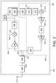
- the hardware subsystem 300 comprises a processing resource 304, for example a processing unit, such as an ARM® core processor, operably coupled to a portion of the transmitter chain 204 and a portion of the receiver chain 206.
- the processing unit 304 supports a test signal control component 306.
- An input of the portion of the transmitter chain 204 which is operably coupled to the processing unit 304, and is capable of communicating with the test signal control component 306, is operably coupled to a test signal generator component 308 having an output that is operably coupled to an input of a gain control component 310; the gain control component 310 is, in this example, an digital gain component and has a first gain control input 312.
- the test signal generator 308 is a tone generator that generates a baseband tone.
- other kinds of signal can be generated to serve as test signals, for example a spread-spectrum signal, and so different waveforms are contemplated.
- test signal generator component 308 can comprise or be operably coupled to a memory (not shown) that stores pre-programmed samples, which can serve as the test signal for transmission at an appropriate data rate.
- a programmable Digital Signal Processor DSP
- DSP Digital Signal Processor
- An output of the gain control component 310 is operably coupled to an input of a Digital-to-Analogue Converter (DAC) component 314, an output of the DAC component 314 being operably coupled to a transmit signal input of a transmit signal mixer component 316.
- the transmit signal mixer component 316 has a transmit local oscillator input 318 for receiving a transmit local oscillator signal.
- An output of the transmit signal mixer component 316 is operably coupled to an input of driver amplifier component 320 having a second gain control input 322. In this example, the driver amplifier component 320 operates in the analogue domain.
- An output of the driver amplifier component 320 is operably coupled to an input of a balun component 324, an output of the balun component 324 being operably coupled to an input of a power amplifier component 326, which in this example also operates in the analogue domain.
- the power amplifier component 326 comprises a third gain control input 328 and an output that is operably coupled to an input a duplexer switch component 330.
- the hardware sub-components can comprise multiple duplexers to support wireless network access to different communications networks operating in different frequency bands.
- the duplexer switch component 330 therefore provides a facility to switch between different duplexers as required by the UE unit 200.
- An output of the duplexer switch component 330 is operably coupled to a transmit side port 332 of the duplexer 208.
- An antenna side port 334 of the duplexer 208 is operably coupled to a coupling port of an antenna switch component 336, another connection port of the antenna switch component 336 being operably coupled to the antenna 210.
- a receive side port 338 of the duplexer 208 is operably coupled to the receiver chain 206, which comprises a low-noise amplifier component 340 having an input operably coupled to the receive side port 338 of the duplexer 208.
- An output of the low-noise amplifier component 340 is operably coupled to a receiver signal input of a receive signal mixer component 342 having a receive local oscillator input 344 for receiving a receive local oscillator signal.
- An output of the receive signal mixer component 342 is operably coupled to an input of an Analogue-to-Digital Converter (ADC) component 346 and an output of the ADC component 346 is operably coupled to the processing unit 304 and, in particular, the test signal control component 306.
- a power measurement component 348 is operably coupled to the output of the ADC component 346 and, separately from the output of the ADC component 346, to test signal control component 306. In another implementation, the measurement of power can be provided in the processing unit 304.
- the assignment of the operational parameter settings is intended to be performed periodically, the frequency of performance of the assignment can be specific to design considerations of the manufacturer of the UE unit 200.
- the assignment of operational parameter settings and indeed measurements required for such assignments are not intended solely to be implemented during factory testing of the UE unit 200 and can be employed "in the field", i.e. at times when the UE unit 200 is deployed in the communications network.
- the test signal control component 306 determines (Step 400) whether a situational condition of the UE unit 200 is satisfied that will permit testing to be performed without disrupting normal operation of the UE unit 200 and/or the communications network.
- the testing relates to isolation provided by the duplexer 208 by way of measurement of power at the receive side port 338 of the duplexer 208 corresponding to the signal applied at the transmit side port 332 of the duplexer 208, and this constitutes signal leakage power.
- the situational conditions can be, for example, when the UE unit 200 is in a factory, such as during factory testing, upon power-up of the UE unit 200 or at an opportunistic time when the transceiver of the UE unit 200 is not otherwise active, i.e. it is not involved in traffic-related communications operations, for example when the transmitter chain 204 is in the transmit OFF state.
- the test signal control component 306 continues to await a suitable opportunity to perform the measurement of the signal leakage power in respect of the duplexer 208. If, however, the UE unit 208 is determined to be in a situational condition compatible with performance of the measurements, for example an opportunity when the transceiver is not otherwise engaged in processing signal traffic, the test signal control component 306 can proceed to testing.
- the test signal control component 306 initiates and controls (Step 402) the process of testing the signal leakage of the duplexer 208. Thereafter, measurements made and any predetermined or pre-stored data is analysed (Step 404) by the test signal control component 306 and then the test signal control component 306 either directly or indirectly implements (Step 406) operational parameter settings of the hardware subsystem 300 that results in a power consumption reduction by the hardware subsystem 300.
- any suitable component or components of the hardware subsystem 300 such as the test signal control component 306 can implement a reduction in an operating voltage of a Voltage Controlled Oscillator (VCO) of the transmitter chain 204, thereby reducing the power consumption of the VCO.
- VCO Voltage Controlled Oscillator
- Another parameter that can be modified is an operating voltage of the low-noise amplifier component 340, because the receiver chain 206 receives less signal power attributable to the transmitter chain 204 as a result of a degree of isolation being achieved that is greater than an expected maximum degree of isolation and so the receiver chain 206 can operate in a mode of operation that exhibits less linearity. This can additionally or alternatively be achieved by reducing the calibration requirements of the receive signal mixer component 342.
- the test signal control component 306 performs measurement of signal power leakage power in a manner common to both methods of assigning operational parameter settings mentioned above.
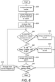
- the test signal control component 306 instructs the antenna switch 336 to disconnect (Step 500) the power amplifier component 326 from the antenna 210.
- the UE unit 200 is designed to operate in multiple frequency bands and so the disconnection of the power amplifier component 326 is achieved by the test signal control component 306 issuing a control signal to the duplexer switch component 330 to connect the power amplifier component 326 to the duplexer 208 and the antenna switch 336 to couple the antenna 210 to another duplexer (not shown).
- the test signal control component 306 then instructs (Step 502) the receiver chain 206 to connect to the duplexer 208, which is the duplexer under test.
- the hardware subsystem 300 of this example comprises a multi-way switch in order to connect the transmitter chain 204 to different duplexer inputs and the receiver chain 206 to different duplexer outputs.
- the test signal control component 306 then configures (Step 504) the test signal generator component 308 in respect of a test tone to be generated and serve as the test signal.
- the test signal is selected to be a tone signal, due to ease of generation and on account of the fact that the test signal can be received by the receiver chain 206 using a very narrow filter, thereby allowing the power of the test signal to be as low as possible.
- the use of other signal types is envisaged, for example a spread-spectrum signal.
- gain parameters of the transmitter chain 204 are set (Step 506) by the test signal control component 306 in order to ensure that the power irradiated at the antenna 210 does not exceed the transmit OFF power threshold of the network mentioned above.
- a first setting is applied at the first gain control input 312 of the gain control component 310
- a second setting is applied at the second gain control input 322 of the driver amplifier component 320
- a third setting is applied at the third gain control input 328 of the power amplifier component 326.
- the test signal control component 306 configures (Step 508) the receiver chain 206 in order to be able to measure the energy of the test signal present at the receive side port 338 of the duplexer 208.
- it can be desirable to offset the receive local oscillator frequency from the transmit local oscillator frequency and hence the receive carrier frequency from the transmit carrier frequency in order to avoid so-called Voltage Controlled Oscillator (VCO) pulling.
- VCO Voltage Controlled Oscillator
- the test signal control component 306 instructs the test signal generator component 308 to generate the test signal and the receiver chain 204 receives a leaked test signal, which is the part of the power of the test signal that is leaked from the transmit side port 332 to the receive side port 338 of the duplexer 208 due to limitations in the isolation of the transmit side port 332 from the receive side port 338 provided by the duplexer 208.
- the power measurement component 348 measures (Step 510) the leaked test signal received by the receiver chain 206, for example by a process of squaring digital samples communicated from the ADC component 346 to the test signal control component 306 and accumulating the results.
- measurement duration and bandwidth of the measurement frequency are selected in advance as a result of experimentation and measurement in order to achieve a balanced trade-off between measurement duration and filter bandwidth, i.e. the ability to distinguish between the test signal and background noise.
- the frequency of the test signal is swept through a range of transmit carrier frequencies within the transmission and reception frequency bands employed by the UE unit 200 in accordance with the LTE or other standards. Consequently, the test signal control component 306 determines (Step 512) whether the frequency of the test signal has been swept through all carrier frequencies at which the tested signal is to be generated and if the test signal still needs to be generated in respect of one or more test frequencies, the test signal control component 306 updates (Step 514) the frequency to be used by the test signal generator component 308 and the above steps of configuring the test signal generator 308, setting the power level of the test signal, configuring the receiver chain 206 and measuring signal leakage (Steps 504 to 510) are repeated until, in this example, testing on all carrier frequencies in the system transmit bandwidth has been completed. By sweeping through a range of carrier frequencies, a profile is obtained of signal leakage power vs. frequency.
- the measurements made as described above in relation to Figure 5 can be used in a first method of assigning operational parameter settings mentioned above.
- the test signal control component 306 analyses (Step 520) the profile of the measured signal leakage power with carrier frequency in order to determine (Step 522) the frequency at which signal leakage power is highest amongst all the measurements of the profile.
- the operation of the test signal control component 306 is based upon a first assumption that the signal isolation provided by the duplexer 208 in practice exceeds a worst case level of isolation specified by the manufacturer of the duplexer 208, and a second assumption that the hardware subsystem 300 is designed to operate in accordance with the LTE standard when the isolation of the duplexer 208 is at the worst case level indicated by the specification of the manufacturer of the duplexer 208.
- the test signal control component 306 then proceeds to analyse the signal leakage power measurements of the profile.
- the test signal control component 306 analyses (Step 524) a first signal leakage power in respect of the first carrier frequency and determines (Step 526) whether the first signal leakage power at the first carrier frequency is better, i.e. lower, than the highest signal leakage power level found previously.
- this step is employed to address a situation where the highest signal leakage level found is being compared with itself.
- this step can be omitted with the use of, for example, suitable software code in order to avoid the possibility of self-comparison in the method.
- the test signal control component 306 assigns (Step 528) a default set of operational parameter settings for the subsystem 300 for transmission of RF signals at the first carrier frequency.
- the default set of operational parameter settings can include settings relating to one or more of the gain control component 310, the driver amplifier component 320 and the power amplifier component 326.
- the test signal control component 306 determines (Step 536) whether other carrier frequencies of the profile require assignment of a set of operational parameter settings, as will be described later herein in greater detail.
- the test signal control component 306 determines (Step 530) whether the level of signal leakage power in respect of the first carrier frequency is lower than the highest level of signal leakage power found by a predetermined margin, for example 5dB. If the predetermined margin is met or exceeded, the test signal control component 306 assigns (Step 532) a non-default set of operational parameters for the subsystem 300 for transmission of RF signals at the first carrier frequency.
- the non-default set of operational parameter settings can include settings relating to one or more of the gain control component 310, the driver amplifier component 320 and the power amplifier component 326.
- the non-default set of operational parameters constitute settings that take advantage of the fact that the duplexer 208 is considered capable of operating with an isolation level greater than that specified by the manufacturer and so the subsystem 300 can be configured to operate in a manner that reduces power consumption by the subsystem 300 on account of the better than specified performance of the duplexer 208. If the predetermined margin has not been met by the level of signal leakage power measured in respect of the first carrier frequency, the test signal control component 306 assigns (Step 534) the default set of operational parameters for transmission of RF signals at the first carrier frequency. This is an example of evaluation of a predetermined power margin criterion.
- the test signal control component 306 determines (Step 536) whether more signal leakage power measurement data remains to be analysed. In the event that more signal leakage power measurement data remains, the test signal control component 306 continues and analyses (Step 538) a signal leakage power measurement associated with a subsequent carrier frequency and executes the assessments in the manner described above in relation to the measured signal leakage power in respect of the first carrier frequency (Steps 526 to 536).
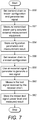
- the test signal control component 306 is then provided with the transmitter chain configuration parameters and associated measurement results for storage (Step 554) for subsequent use. Subsequently, the receiver chain 206 is configured (Step 556) using known configuration parameters. Using an external signal generator in place of the antenna 210, a test signal is generated (Step 558) having a precisely known power level. The accurate test signal generated external to the UE unit 200 as received by the receiver chain 206 is measured (Step 560) by the power measurement component 348.
- the accurately known test signal power level and the associated measurement thereof are provided to the test signal control component 306 for storage (Step 562) and subsequent use.
- the signal leakage power measurements made to generate the signal leakage profile which are simply measurements of power of received leaked signals varying with frequency, are converted to absolute values using the measurements made as described above in relation to Figure 7 .
- the measured signal leakage powers stored against changes in frequency simply provide a profile of relative values without a point of reference.
- the test signal control component 306 accesses (Step 570) a measured signal leakage power level from the profile in respect of a first carrier frequency in the profile.
- the test signal control component 306 then accesses (Step 572), in respect of the carrier frequency of the accessed measured signal leakage power value, the precisely measured transmit power that was measured in the factory and then calculates the gain of the receiver chain 206 using the measurements made in the factory with accurate measurement apparatus. Thereafter, the test signal control component 306 uses the calculated gain of the receiver chain 206 to normalise (Step 574) the measured signal leakage power level in order to obtain a more accurate measurement, albeit still an estimate, of the measured signal leakage power level at the first carrier frequency.
- the test signal control component 306 subtracts (Step 576) the normalised measured signal leakage power from the accurate measurement of the test signal power in order to yield an estimate of the isolation of the duplexer 208 in respect of the first carrier frequency.
- the estimated isolation value and the frequency to which it corresponds is then stored (Step 578) by the test signal control component 306. Thereafter, the test signal control component 306 determines (Step 580) whether more measurements need to be converted to absolute isolation estimates in respect of other carrier frequencies.
- test signal control component 306 access (Step 582) the next measured signal leakage power in respect of the next carrier frequency to be processed and the above process (Steps 572 to 580) of using accurate measurements to generate an estimate of absolute isolation of the duplexer 208 at a respective carrier frequency is performed until no further signal leakage power measurements need to be converted to absolute isolation estimates.
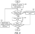
- the test signal control component 306 next assigns operational parameter sets to each of the carrier frequencies based upon the isolation estimate associated with the carrier frequency. In this respect, the test signal control component 306 accesses (Step 800) the first isolation estimate stored in respect of the first carrier frequency of the profile and determines (Step 802) whether the isolation estimate is below or equal to a predetermined threshold value. This is another example of evaluation of a predetermined power margin criterion.
- the isolation estimated is considered to be sufficiently close to the minimum isolation specified by the manufacturer of the duplexer 208 not to merit employing operational parameter settings in the hardware subsystem 300 to try to reduce power consumption by the hardware subsystem 300. Consequently, the test signal control component 306 assigns (Step 804) the default set of operational parameter settings for when the transmit chain 204 uses the first carrier frequency. The test signal control, component 306 the proceeds to determine (Step 808) whether more carrier frequencies need to have operational parameter settings assigned to them, as will be described in further detail hereinbelow.
- the test signal control component 306 assigns (Step 806) a non-default set of operational parameter settings for the hardware subsystem 300 in order to reduce power consumption by the hardware subsystem 300 when the transmit chain 204 uses the first carrier frequency. Thereafter, the test signal control component 306 determines (Step 808) whether more carrier frequencies need to have operational parameter settings assigned to them.
- test signal control component 306 retrieves (Step 810) a next isolation estimate in respect of a next carrier frequency of the profile and the above process (Steps 802 to 808) of assessing the estimated isolation of the duplexer 208 and assigning appropriate sets of operational parameter settings is performed until no further carrier frequencies in the profile need assignment of operational parameter settings.
- a set of parameters can comprise one or more parameters.
- the number of parameters and the nature of the parameters for example analogue or digital, can be selected depending upon implementation practicalities.
- duplexers are not intended to be limiting in respect of a particular design or technology to achieve frequency segregation of signals and any suitable component is contemplated that can provide sufficient signal isolation between the transmitter chain and receiver chain, which are both coupled to the duplexer and simultaneously connect the transmitter chain and the receiver chain to an antenna, for example a so-called "hybrid junction".
- the antenna 210 can be coupled to any of a number of available duplexing components depending upon a desired frequency band of operation of the UE unit 200 and so decoupling of the antenna 210 from a duplexing component to be tested can be achieved by coupling the antenna 210 to a different duplexing component that is not being tested.
- the antenna switch component 336 can be configured to create an open circuit between a duplexing component being tested and the antenna 210, for example where hardware subsystem 300 comprises a single duplexing component.
- the antenna 210 cannot be decoupled from the duplexing component 208, it is necessary to set appropriate adjustable parameters of the transmit chain 204 to generate the test signal so as to have a power level that does not result in the transmit OFF threshold being exceeded when the test signal is irradiated by the antenna 210.
- downlink refers to communications from an eNode B to a UE unit.
- the UE unit 200 therefore possesses, in the examples set forth herein, a downlink receiver chain.
- uplink refers to communications from a UE unit to an eNode B.
- the UE unit 200 therefore possesses, in the examples set forth herein, an uplink transmitter chain.
- the systems and methods of the above embodiments may be implemented in a computer system (in particular in computer hardware or in computer software) or in specifically manufactured or adapted integrated circuits, in addition to the structural components and user interactions described.
- the methods of the above embodiments may be provided as computer programs or as computer program products or computer readable media carrying a computer program which is arranged, when run on a computer or other processor, to perform the method(s) described above.
- computer readable media includes, without limitation, any medium or media which can be read and accessed directly by a computer or computer system.
- the media can include, but are not limited to, magnetic storage media such as floppy discs, hard disc storage media and magnetic tape; optical storage media such as optical discs or CD-ROMs; electrical storage media such as memory, including RAM, ROM and flash memory; and hybrids and combinations of the above such as magnetic/optical storage media.
Landscapes
- Engineering & Computer Science (AREA)
- Computer Networks & Wireless Communication (AREA)
- Signal Processing (AREA)
- Physics & Mathematics (AREA)
- Electromagnetism (AREA)
- Quality & Reliability (AREA)
- Mobile Radio Communication Systems (AREA)
- Transceivers (AREA)
Claims (15)
- Appareil de communication configuré pour procurer un accès à un réseau sans fil conformément à une norme de communication qui spécifie une condition de seuil de puissance lorsque l'émission est désactivée, à savoir un niveau de puissance qui est défini comme étant une puissance d'émission maximale que l'appareil de communication peut émettre lorsqu'il se trouve dans un état de non émission ou dans un état désactivé, l'appareil comprenant :un sous-système matériel (300) comprenant un composant faisant office de commande d'un signal test (306), un composant (208) faisant office de duplexeur et des composants de traitement radiofréquence (302), les composants de traitement radiofréquence (302) comprenant : etune portion faisant office de chaîne d'émission (204) dont une sortie est couplée de manière opérationnelle à un port côté émission (332) du composant (208) faisant office de duplexeur ;une portion faisant office de chaîne de réception (206) à laquelle est associé un seuil de sensibilité de signal et qui est couplée de manière opérationnelle à un port côté réception (338) du composant (208) faisant office de duplexeur ;dans lequel le composant (306) faisant office de commande d'un signal test est conçu pour coopérer avec la portion faisant office de chaîne d'émission (204) afin de générer un signal test, une portion du signal test étant apte à fuiter par l'intermédiaire du composant (208) faisant office de duplexeur depuis son port côté émission (338) jusqu'à son port côté réception (338) ;caractérisé en ce que
le composant (306) faisant office de commande du signal test est configuré pour garantir le fait que n'importe quelle puissance émise du signal test répond à la condition de seuil de puissance lorsque l'émission est désactivée et la portion du signal test qui a fuité est supérieure au seuil de sensibilité de signal de la portion faisant office de chaîne de réception (206). - Appareil selon la revendication 1, comprenant en outre :une antenne (210) ; dans lequelle composant (306) faisant office de commande du signal test est conçu pour générer un signal de commande de non émission avant la génération du signal test.
- Appareil selon la revendication 2, dans lequel le sous-système matériel (300) est conçu pour découpler l'antenne (210) par rapport au composant (208) faisant office de duplexeur en réponse au signal de commande de non émission.
- Appareil selon la revendication 3, comprenant en outre :un autre composant faisant office de duplexeur ; dans lequelle sous-système matériel (300) est conçu pour coupler l'antenne (210) à l'autre composant faisant office de duplexeur à la place du composant (208) faisant office de duplexeur en réponse au signal de commande de non émission.
- Appareil selon l'une quelconque des revendications précédentes, dans lequel le composant (306) faisant office de commande du signal test est conçu pour coopérer avec la portion (206) faisant office de chaîne de réception dans le but de commander la réception du signal test par l'intermédiaire de la portion (206) faisant office de chaîne de réception.
- Appareil selon l'une quelconque des revendications précédentes, dans lequel le sous-système matériel (300) comprend en outre un composant (348) ayant pour objet la mesure de l'intensité du signal et le composant (306) faisant office de commande du signal test est conçu pour coopérer avec le composant (348) ayant pour objet la mesure de l'intensité du signal dans le but de mesurer une puissance du signal de réception par rapport au signal test tel qu'il est reçu par la portion (206) faisant office de chaîne de réception.
- Appareil selon la revendication 6, dans lequel le composant (306) faisant office de commande du signal test est conçu pour coopérer avec la portion (204) faisant office de chaîne d'émission dans le but de générer un certain nombre de signaux test par rapport à plusieurs fréquences porteuses d'émission au sein d'une largeur de bande d'émission du système, et pour coopérer avec le composant (348) ayant pour objet la mesure de l'intensité du signal dans le but de mesurer la puissance de signal de fuite par rapport à chacune desdites plusieurs fréquences porteuses d'émission.
- Appareil selon la revendication 7, dans lequel le composant (306) faisant office de commande du signal test est conçu pour générer un profil de fuite de signal représentant la puissance des signaux ayant fuité par l'intermédiaire du composant (208) faisant office de duplexeur par rapport à chacune desdites plusieurs fréquences porteuses d'émission.
- Appareil selon l'une quelconque des revendications précédentes, dans lequel le sous-système matériel (300) possède un ensemble par défaut d'une configuration de paramètres opérationnels et un ensemble non par défaut d'une configuration de paramètres opérationnels qui y est associé, par rapport à l'exploitation du sous-système matériel (300), et à l'ensemble non par défaut de la configuration de paramètres opérationnels est associée une consommation de puissance réduite par rapport à celle de l'ensemble par défaut de la configuration de paramètres opérationnels.
- Appareil selon la revendication 9, lorsqu'elle dépend de la revendication 8, dans lequel le composant (306) faisant office de commande du signal test est conçu pour analyser le profil de fuite du signal et pour utiliser des différences relatives quant à la puissance mesurée du signal de fuite, entre des fréquences porteuses, dans le but de déterminer le fait de savoir si il y a lieu d'appliquer l'ensemble non par défaut de la configuration de paramètres opérationnels sur base des fréquences porteuses une à une.
- Appareil selon la revendication 10, dans lequel le composant (306) faisant office de commande du signal test est conçu pour analyser le profil de fuite du signal et pour en sélectionner une puissance mesurée la plus basse du signal de fuite et pour attribuer l'ensemble non par défaut de la configuration de paramètres opérationnels à des fins d'émission de fréquences porteuses dont la puissance de fuite mesurée du signal répond à un critère marginal de puissance prédéterminé par rapport à la puissance mesurée la plus basse du signal de fuite.
- Appareil selon l'une quelconque des revendications précédentes, comprenant en outre une banque de données conçue pour la mise en mémoire de plusieurs valeurs de gains de réception de référence par rapport à plusieurs fréquences porteuses de réception respectives et plusieurs valeurs de puissance d'émission de référence par rapport à plusieurs fréquences porteuses d'émission respectives.
- Appareil selon la revendication 12, lorsqu'elle dépend de la revendication 7, dans lequel le composant (306) faisant office de commande du signal test est conçu pour accéder à la banque de données et pour utiliser, par rapport à une fréquence porteuse sélectionnée :une valeur de gain de réception de référence choisie parmi lesdites plusieurs valeurs de gains de réception de référence ;une valeur de puissance d'émission de référence choisie parmi lesdites plusieurs valeurs de puissance d'émission de référence ; etune puissance mesurée de signal de fuite choisie parmi lesdites puissances mesurées du signal de fuite ;dans le but de générer une estimation de l'isolation du composant (208) faisant office de duplexeur à la fréquence porteuse d'émission sélectionnée.
- Appareil selon la revendication 13, dans lequel le sous-système matériel (300) possède un ensemble par défaut de configuration des paramètres opérationnels et un ensemble non par défaut de configuration des paramètres opérationnels associé au premier cité en liaison avec l'exploitation du sous-système matériel (300), et à l'ensemble non par défaut de la configuration de paramètres opérationnels est associée une consommation de puissance réduite par rapport à celle de l'ensemble par défaut de la configuration de paramètres opérationnels.
- Procédé de détermination d'un profil de fuite de signal d'un composant (208) faisant office de duplexeur dans un appareil de communication conçu pour procurer un accès à un réseau sans fil conformément à une norme de communication qui spécifie une condition de seuil de puissance lorsque l'émission est désactivée, à savoir un niveau de puissance qui est défini comme étant une puissance d'émission maximale que l'appareil de communication peut émettre lorsqu'il se trouve dans un état de non émission ou dans un état désactivé, le procédé comprenant :un composant faisant office de commande d'un signal test (306) qui commande la génération d'un signal test ;une portion faisant office de chaîne d'émission (204) qui génère le signal test en réponse au composant faisant office de commande d'un signal test (306) ;la propagation du signal test au composant (208) faisant office de duplexeur ;une portion faisant office de chaîne de réception (206) à laquelle est associé un seuil de sensibilité de signal, qui reçoit une portion du signal qui a fuité à partir du composant (208) faisant office de duplexeur en réponse au fait que le signal test est en train d'être appliqué au composant (208) faisant office de duplexeur ; etun composant (348) ayant pour objet la mesure de l'intensité du signal, qui mesure la puissance du signal de fuite reçu par la portion faisant office de chaîne de réception (206) ;dans lequel le procédé est caractérisé par le fait que
le composant faisant office de commande d'un signal test (306) garantit le fait que n'importe quelle puissance émise du signal test répond à la condition de seuil de puissance lorsque l'émission est désactivée et qu'une portion du signal test qui a fuité est supérieure au seuil de sensibilité de signal de la portion faisant office de chaîne de réception (206).
Applications Claiming Priority (1)
| Application Number | Priority Date | Filing Date | Title |
|---|---|---|---|
| PCT/EP2015/071132 WO2017045707A1 (fr) | 2015-09-15 | 2015-09-15 | Appareil de communication, système de communication et procédé de détermination d'isolement de signal |
Publications (2)
| Publication Number | Publication Date |
|---|---|
| EP3350932A1 EP3350932A1 (fr) | 2018-07-25 |
| EP3350932B1 true EP3350932B1 (fr) | 2019-11-20 |
Family
ID=54288752
Family Applications (1)
| Application Number | Title | Priority Date | Filing Date |
|---|---|---|---|
| EP15777883.8A Active EP3350932B1 (fr) | 2015-09-15 | 2015-09-15 | Appareil de communication, système de communication et procédé pour la détermination de l'isolation d'un signal |
Country Status (5)
| Country | Link |
|---|---|
| US (1) | US10419061B2 (fr) |
| EP (1) | EP3350932B1 (fr) |
| JP (1) | JP6668458B2 (fr) |
| CN (1) | CN108028677B (fr) |
| WO (1) | WO2017045707A1 (fr) |
Cited By (1)
| Publication number | Priority date | Publication date | Assignee | Title |
|---|---|---|---|---|
| US20230076071A1 (en) * | 2021-09-09 | 2023-03-09 | Qualcomm Incorporated | Transmit diversity power leakage detection and filtering in antenna compensator power detector |
Families Citing this family (6)
| Publication number | Priority date | Publication date | Assignee | Title |
|---|---|---|---|---|
| US10505645B2 (en) * | 2017-05-23 | 2019-12-10 | Renesas Electronics Corporation | Wireless communication device and determination method |
| TWI707553B (zh) * | 2019-09-09 | 2020-10-11 | 瑞昱半導體股份有限公司 | 射頻電路 |
| CN112491436B (zh) * | 2019-09-12 | 2022-04-26 | 瑞昱半导体股份有限公司 | 射频电路 |
| CN111404619B (zh) * | 2020-03-10 | 2024-04-30 | 中国人民解放军32181部队 | 一种复杂电磁环境下指控通信保障设备 |
| TWI733530B (zh) * | 2020-07-21 | 2021-07-11 | 瑞昱半導體股份有限公司 | 隔離度估計系統、方法以及處理電路 |
| KR102293420B1 (ko) * | 2020-11-26 | 2021-08-25 | 한화시스템 주식회사 | 주파수 분할 방식의 위상배열 안테나 장치 및 이의 작동방법 |
Family Cites Families (12)
| Publication number | Priority date | Publication date | Assignee | Title |
|---|---|---|---|---|
| US7760080B2 (en) * | 2000-09-08 | 2010-07-20 | Automotive Technologies International, Inc. | Tire monitoring with passive and active modes |
| KR100974454B1 (ko) * | 2004-01-12 | 2010-08-06 | 넥스티비티 인코포레이티드 | 단거리 셀룰러 부스터 |
| CN101453226B (zh) * | 2007-11-30 | 2013-07-10 | 松下电器产业株式会社 | 本振泄漏消除装置及方法 |
| US9496620B2 (en) * | 2013-02-04 | 2016-11-15 | Ubiquiti Networks, Inc. | Radio system for long-range high-speed wireless communication |
| US8842582B2 (en) | 2010-06-04 | 2014-09-23 | Qualcomm Incorporated | Reducing power consumption by taking advantage of superior in-circuit duplexer performance |
| EP2503703A1 (fr) * | 2011-02-25 | 2012-09-26 | Telefonaktiebolaget LM Ericsson (publ) | Technique d'adaptation d'émetteur-récepteur radio |
| US8879667B2 (en) * | 2011-07-01 | 2014-11-04 | Intel Corporation | Layer shifting in open loop multiple-input, multiple-output communications |
| EP2730036B1 (fr) * | 2011-07-08 | 2019-07-03 | Google LLC | Commande du taux sar dans des systèmes de diversité de transmission mobiles employant une formation de faisceau par utilisation d'un couplage entre des branches de diversité |
| KR101763997B1 (ko) * | 2012-04-12 | 2017-08-01 | 스카이워크스 솔루션즈, 인코포레이티드 | 전송 무선 주파수 신호와 수신 무선 주파수 신호 간의 개선된 격리에 관한 시스템 및 방법 |
| US9531418B2 (en) * | 2012-08-07 | 2016-12-27 | Google Technology Holdings LLC | Tunable inter-antenna isolation |
| US9444559B2 (en) | 2013-06-03 | 2016-09-13 | Futurewei Technologies, Inc. | Second order intercept point (IP2) calibration for wireless receivers |
| US9374127B2 (en) * | 2013-12-16 | 2016-06-21 | Broadcom Corporation | Balancing method of tunable duplexer |
-
2015
- 2015-09-15 EP EP15777883.8A patent/EP3350932B1/fr active Active
- 2015-09-15 US US15/758,179 patent/US10419061B2/en active Active
- 2015-09-15 WO PCT/EP2015/071132 patent/WO2017045707A1/fr not_active Ceased
- 2015-09-15 JP JP2018511650A patent/JP6668458B2/ja active Active
- 2015-09-15 CN CN201580083152.5A patent/CN108028677B/zh active Active
Non-Patent Citations (1)
| Title |
|---|
| None * |
Cited By (2)
| Publication number | Priority date | Publication date | Assignee | Title |
|---|---|---|---|---|
| US20230076071A1 (en) * | 2021-09-09 | 2023-03-09 | Qualcomm Incorporated | Transmit diversity power leakage detection and filtering in antenna compensator power detector |
| US11901931B2 (en) * | 2021-09-09 | 2024-02-13 | Qualcomm Incorporated | Transmit diversity power leakage detection and filtering in antenna compensator power detector |
Also Published As
| Publication number | Publication date |
|---|---|
| JP2018533260A (ja) | 2018-11-08 |
| US20180254795A1 (en) | 2018-09-06 |
| CN108028677A (zh) | 2018-05-11 |
| CN108028677B (zh) | 2020-07-31 |
| WO2017045707A1 (fr) | 2017-03-23 |
| JP6668458B2 (ja) | 2020-03-18 |
| US10419061B2 (en) | 2019-09-17 |
| EP3350932A1 (fr) | 2018-07-25 |
Similar Documents
| Publication | Publication Date | Title |
|---|---|---|
| EP3350932B1 (fr) | Appareil de communication, système de communication et procédé pour la détermination de l'isolation d'un signal | |
| KR101419420B1 (ko) | 기지국 캘리브레이션 | |
| US20190222326A1 (en) | Scheduling for power amplifier characterization | |
| JP6042934B2 (ja) | マルチバンドマルチキャリア無線システムのための動的アンテナ同調 | |
| EP2474099B1 (fr) | Scanner de l'environnement radio | |
| US9241336B2 (en) | Communication terminal device and method, base station device, and communication system | |
| US10382091B2 (en) | Methods and apparatus for improving performance based on filter characteristics | |
| EP3202199B1 (fr) | Détermination d'une fréquence centrale dans une bande de fréquence sans licence à utiliser | |
| CN105379130B (zh) | 与无线电信号的接收有关的方法和设备 | |
| US20240196335A1 (en) | Network control of sensitivity degradation | |
| CN114040421B (zh) | 一种无线资源测量方法及装置 | |
| US10784919B2 (en) | Adaptation circuit for a transceiver | |
| US20140233621A1 (en) | Gsm/edge transmit power calibration and characterized digital predistortion calibration using multi-band multi-channel multi-chain sweep | |
| TW202547148A (zh) | 一種通信方法、裝置和系統 | |
| TW202549392A (zh) | 使用子頻帶傳輸功率限制的射頻暴露合規性 |
Legal Events
| Date | Code | Title | Description |
|---|---|---|---|
| STAA | Information on the status of an ep patent application or granted ep patent |
Free format text: STATUS: THE INTERNATIONAL PUBLICATION HAS BEEN MADE |
|
| PUAI | Public reference made under article 153(3) epc to a published international application that has entered the european phase |
Free format text: ORIGINAL CODE: 0009012 |
|
| STAA | Information on the status of an ep patent application or granted ep patent |
Free format text: STATUS: REQUEST FOR EXAMINATION WAS MADE |
|
| 17P | Request for examination filed |
Effective date: 20180320 |
|
| AK | Designated contracting states |
Kind code of ref document: A1 Designated state(s): AL AT BE BG CH CY CZ DE DK EE ES FI FR GB GR HR HU IE IS IT LI LT LU LV MC MK MT NL NO PL PT RO RS SE SI SK SM TR |
|
| AX | Request for extension of the european patent |
Extension state: BA ME |
|
| DAV | Request for validation of the european patent (deleted) | ||
| DAX | Request for extension of the european patent (deleted) | ||
| GRAP | Despatch of communication of intention to grant a patent |
Free format text: ORIGINAL CODE: EPIDOSNIGR1 |
|
| STAA | Information on the status of an ep patent application or granted ep patent |
Free format text: STATUS: GRANT OF PATENT IS INTENDED |
|
| INTG | Intention to grant announced |
Effective date: 20190603 |
|
| GRAA | (expected) grant |
Free format text: ORIGINAL CODE: 0009210 |
|
| STAA | Information on the status of an ep patent application or granted ep patent |
Free format text: STATUS: THE PATENT HAS BEEN GRANTED |
|
| GRAS | Grant fee paid |
Free format text: ORIGINAL CODE: EPIDOSNIGR3 |
|
| AK | Designated contracting states |
Kind code of ref document: B1 Designated state(s): AL AT BE BG CH CY CZ DE DK EE ES FI FR GB GR HR HU IE IS IT LI LT LU LV MC MK MT NL NO PL PT RO RS SE SI SK SM TR |
|
| REG | Reference to a national code |
Ref country code: GB Ref legal event code: FG4D |
|
| REG | Reference to a national code |
Ref country code: CH Ref legal event code: EP |
|
| REG | Reference to a national code |
Ref country code: IE Ref legal event code: FG4D |
|
| REG | Reference to a national code |
Ref country code: DE Ref legal event code: R096 Ref document number: 602015042126 Country of ref document: DE |
|
| REG | Reference to a national code |
Ref country code: AT Ref legal event code: REF Ref document number: 1205353 Country of ref document: AT Kind code of ref document: T Effective date: 20191215 |
|
| REG | Reference to a national code |
Ref country code: NL Ref legal event code: MP Effective date: 20191120 |
|
| REG | Reference to a national code |
Ref country code: LT Ref legal event code: MG4D |
|
| PG25 | Lapsed in a contracting state [announced via postgrant information from national office to epo] |
Ref country code: LT Free format text: LAPSE BECAUSE OF FAILURE TO SUBMIT A TRANSLATION OF THE DESCRIPTION OR TO PAY THE FEE WITHIN THE PRESCRIBED TIME-LIMIT Effective date: 20191120 Ref country code: NO Free format text: LAPSE BECAUSE OF FAILURE TO SUBMIT A TRANSLATION OF THE DESCRIPTION OR TO PAY THE FEE WITHIN THE PRESCRIBED TIME-LIMIT Effective date: 20200220 Ref country code: GR Free format text: LAPSE BECAUSE OF FAILURE TO SUBMIT A TRANSLATION OF THE DESCRIPTION OR TO PAY THE FEE WITHIN THE PRESCRIBED TIME-LIMIT Effective date: 20200221 Ref country code: SE Free format text: LAPSE BECAUSE OF FAILURE TO SUBMIT A TRANSLATION OF THE DESCRIPTION OR TO PAY THE FEE WITHIN THE PRESCRIBED TIME-LIMIT Effective date: 20191120 Ref country code: LV Free format text: LAPSE BECAUSE OF FAILURE TO SUBMIT A TRANSLATION OF THE DESCRIPTION OR TO PAY THE FEE WITHIN THE PRESCRIBED TIME-LIMIT Effective date: 20191120 Ref country code: NL Free format text: LAPSE BECAUSE OF FAILURE TO SUBMIT A TRANSLATION OF THE DESCRIPTION OR TO PAY THE FEE WITHIN THE PRESCRIBED TIME-LIMIT Effective date: 20191120 Ref country code: BG Free format text: LAPSE BECAUSE OF FAILURE TO SUBMIT A TRANSLATION OF THE DESCRIPTION OR TO PAY THE FEE WITHIN THE PRESCRIBED TIME-LIMIT Effective date: 20200220 Ref country code: FI Free format text: LAPSE BECAUSE OF FAILURE TO SUBMIT A TRANSLATION OF THE DESCRIPTION OR TO PAY THE FEE WITHIN THE PRESCRIBED TIME-LIMIT Effective date: 20191120 |
|
| PG25 | Lapsed in a contracting state [announced via postgrant information from national office to epo] |
Ref country code: IS Free format text: LAPSE BECAUSE OF FAILURE TO SUBMIT A TRANSLATION OF THE DESCRIPTION OR TO PAY THE FEE WITHIN THE PRESCRIBED TIME-LIMIT Effective date: 20200320 Ref country code: HR Free format text: LAPSE BECAUSE OF FAILURE TO SUBMIT A TRANSLATION OF THE DESCRIPTION OR TO PAY THE FEE WITHIN THE PRESCRIBED TIME-LIMIT Effective date: 20191120 Ref country code: RS Free format text: LAPSE BECAUSE OF FAILURE TO SUBMIT A TRANSLATION OF THE DESCRIPTION OR TO PAY THE FEE WITHIN THE PRESCRIBED TIME-LIMIT Effective date: 20191120 |
|
| PG25 | Lapsed in a contracting state [announced via postgrant information from national office to epo] |
Ref country code: AL Free format text: LAPSE BECAUSE OF FAILURE TO SUBMIT A TRANSLATION OF THE DESCRIPTION OR TO PAY THE FEE WITHIN THE PRESCRIBED TIME-LIMIT Effective date: 20191120 |
|
| PG25 | Lapsed in a contracting state [announced via postgrant information from national office to epo] |
Ref country code: EE Free format text: LAPSE BECAUSE OF FAILURE TO SUBMIT A TRANSLATION OF THE DESCRIPTION OR TO PAY THE FEE WITHIN THE PRESCRIBED TIME-LIMIT Effective date: 20191120 Ref country code: PT Free format text: LAPSE BECAUSE OF FAILURE TO SUBMIT A TRANSLATION OF THE DESCRIPTION OR TO PAY THE FEE WITHIN THE PRESCRIBED TIME-LIMIT Effective date: 20200412 Ref country code: RO Free format text: LAPSE BECAUSE OF FAILURE TO SUBMIT A TRANSLATION OF THE DESCRIPTION OR TO PAY THE FEE WITHIN THE PRESCRIBED TIME-LIMIT Effective date: 20191120 Ref country code: ES Free format text: LAPSE BECAUSE OF FAILURE TO SUBMIT A TRANSLATION OF THE DESCRIPTION OR TO PAY THE FEE WITHIN THE PRESCRIBED TIME-LIMIT Effective date: 20191120 Ref country code: CZ Free format text: LAPSE BECAUSE OF FAILURE TO SUBMIT A TRANSLATION OF THE DESCRIPTION OR TO PAY THE FEE WITHIN THE PRESCRIBED TIME-LIMIT Effective date: 20191120 Ref country code: DK Free format text: LAPSE BECAUSE OF FAILURE TO SUBMIT A TRANSLATION OF THE DESCRIPTION OR TO PAY THE FEE WITHIN THE PRESCRIBED TIME-LIMIT Effective date: 20191120 |
|
| REG | Reference to a national code |
Ref country code: CH Ref legal event code: PL |
|
| REG | Reference to a national code |
Ref country code: AT Ref legal event code: MK05 Ref document number: 1205353 Country of ref document: AT Kind code of ref document: T Effective date: 20191120 |
|
| REG | Reference to a national code |
Ref country code: DE Ref legal event code: R097 Ref document number: 602015042126 Country of ref document: DE |
|
| PG25 | Lapsed in a contracting state [announced via postgrant information from national office to epo] |
Ref country code: SM Free format text: LAPSE BECAUSE OF FAILURE TO SUBMIT A TRANSLATION OF THE DESCRIPTION OR TO PAY THE FEE WITHIN THE PRESCRIBED TIME-LIMIT Effective date: 20191120 Ref country code: SK Free format text: LAPSE BECAUSE OF FAILURE TO SUBMIT A TRANSLATION OF THE DESCRIPTION OR TO PAY THE FEE WITHIN THE PRESCRIBED TIME-LIMIT Effective date: 20191120 |
|
| PLBE | No opposition filed within time limit |
Free format text: ORIGINAL CODE: 0009261 |
|
| STAA | Information on the status of an ep patent application or granted ep patent |
Free format text: STATUS: NO OPPOSITION FILED WITHIN TIME LIMIT |
|
| 26N | No opposition filed |
Effective date: 20200821 |
|
| PG25 | Lapsed in a contracting state [announced via postgrant information from national office to epo] |
Ref country code: LI Free format text: LAPSE BECAUSE OF THE APPLICANT RENOUNCES Effective date: 20200810 Ref country code: SI Free format text: LAPSE BECAUSE OF FAILURE TO SUBMIT A TRANSLATION OF THE DESCRIPTION OR TO PAY THE FEE WITHIN THE PRESCRIBED TIME-LIMIT Effective date: 20191120 Ref country code: CH Free format text: LAPSE BECAUSE OF THE APPLICANT RENOUNCES Effective date: 20200810 Ref country code: AT Free format text: LAPSE BECAUSE OF FAILURE TO SUBMIT A TRANSLATION OF THE DESCRIPTION OR TO PAY THE FEE WITHIN THE PRESCRIBED TIME-LIMIT Effective date: 20191120 Ref country code: PL Free format text: LAPSE BECAUSE OF FAILURE TO SUBMIT A TRANSLATION OF THE DESCRIPTION OR TO PAY THE FEE WITHIN THE PRESCRIBED TIME-LIMIT Effective date: 20191120 |
|
| PG25 | Lapsed in a contracting state [announced via postgrant information from national office to epo] |
Ref country code: IT Free format text: LAPSE BECAUSE OF FAILURE TO SUBMIT A TRANSLATION OF THE DESCRIPTION OR TO PAY THE FEE WITHIN THE PRESCRIBED TIME-LIMIT Effective date: 20191120 |
|
| REG | Reference to a national code |
Ref country code: BE Ref legal event code: MM Effective date: 20200930 |
|
| PG25 | Lapsed in a contracting state [announced via postgrant information from national office to epo] |
Ref country code: LU Free format text: LAPSE BECAUSE OF NON-PAYMENT OF DUE FEES Effective date: 20200915 |
|
| PG25 | Lapsed in a contracting state [announced via postgrant information from national office to epo] |
Ref country code: BE Free format text: LAPSE BECAUSE OF NON-PAYMENT OF DUE FEES Effective date: 20200930 Ref country code: IE Free format text: LAPSE BECAUSE OF NON-PAYMENT OF DUE FEES Effective date: 20200915 |
|
| PG25 | Lapsed in a contracting state [announced via postgrant information from national office to epo] |
Ref country code: TR Free format text: LAPSE BECAUSE OF FAILURE TO SUBMIT A TRANSLATION OF THE DESCRIPTION OR TO PAY THE FEE WITHIN THE PRESCRIBED TIME-LIMIT Effective date: 20191120 Ref country code: MT Free format text: LAPSE BECAUSE OF FAILURE TO SUBMIT A TRANSLATION OF THE DESCRIPTION OR TO PAY THE FEE WITHIN THE PRESCRIBED TIME-LIMIT Effective date: 20191120 Ref country code: CY Free format text: LAPSE BECAUSE OF FAILURE TO SUBMIT A TRANSLATION OF THE DESCRIPTION OR TO PAY THE FEE WITHIN THE PRESCRIBED TIME-LIMIT Effective date: 20191120 |
|
| PG25 | Lapsed in a contracting state [announced via postgrant information from national office to epo] |
Ref country code: MK Free format text: LAPSE BECAUSE OF FAILURE TO SUBMIT A TRANSLATION OF THE DESCRIPTION OR TO PAY THE FEE WITHIN THE PRESCRIBED TIME-LIMIT Effective date: 20191120 Ref country code: MC Free format text: LAPSE BECAUSE OF FAILURE TO SUBMIT A TRANSLATION OF THE DESCRIPTION OR TO PAY THE FEE WITHIN THE PRESCRIBED TIME-LIMIT Effective date: 20191120 |
|
| PGFP | Annual fee paid to national office [announced via postgrant information from national office to epo] |
Ref country code: DE Payment date: 20250919 Year of fee payment: 11 |
|
| PGFP | Annual fee paid to national office [announced via postgrant information from national office to epo] |
Ref country code: GB Payment date: 20250919 Year of fee payment: 11 |
|
| PGFP | Annual fee paid to national office [announced via postgrant information from national office to epo] |
Ref country code: FR Payment date: 20250922 Year of fee payment: 11 |