EP3352217A2 - Anzeigevorrichtung und verfahren zur herstellung von anzeigevorrichtung - Google Patents
Anzeigevorrichtung und verfahren zur herstellung von anzeigevorrichtung Download PDFInfo
- Publication number
- EP3352217A2 EP3352217A2 EP17209569.7A EP17209569A EP3352217A2 EP 3352217 A2 EP3352217 A2 EP 3352217A2 EP 17209569 A EP17209569 A EP 17209569A EP 3352217 A2 EP3352217 A2 EP 3352217A2
- Authority
- EP
- European Patent Office
- Prior art keywords
- light
- adhesion film
- layer
- emitting components
- substrate
- Prior art date
- Legal status (The legal status is an assumption and is not a legal conclusion. Google has not performed a legal analysis and makes no representation as to the accuracy of the status listed.)
- Granted
Links
Images











Classifications
-
- H—ELECTRICITY
- H10—SEMICONDUCTOR DEVICES; ELECTRIC SOLID-STATE DEVICES NOT OTHERWISE PROVIDED FOR
- H10H—INORGANIC LIGHT-EMITTING SEMICONDUCTOR DEVICES HAVING POTENTIAL BARRIERS
- H10H29/00—Integrated devices, or assemblies of multiple devices, comprising at least one light-emitting semiconductor element covered by group H10H20/00
- H10H29/10—Integrated devices comprising at least one light-emitting semiconductor component covered by group H10H20/00
- H10H29/14—Integrated devices comprising at least one light-emitting semiconductor component covered by group H10H20/00 comprising multiple light-emitting semiconductor components
- H10H29/142—Two-dimensional arrangements, e.g. asymmetric LED layout
-
- G—PHYSICS
- G09—EDUCATION; CRYPTOGRAPHY; DISPLAY; ADVERTISING; SEALS
- G09F—DISPLAYING; ADVERTISING; SIGNS; LABELS OR NAME-PLATES; SEALS
- G09F9/00—Indicating arrangements for variable information in which the information is built-up on a support by selection or combination of individual elements
- G09F9/30—Indicating arrangements for variable information in which the information is built-up on a support by selection or combination of individual elements in which the desired character or characters are formed by combining individual elements
- G09F9/33—Indicating arrangements for variable information in which the information is built-up on a support by selection or combination of individual elements in which the desired character or characters are formed by combining individual elements being semiconductor devices, e.g. diodes
-
- H—ELECTRICITY
- H10—SEMICONDUCTOR DEVICES; ELECTRIC SOLID-STATE DEVICES NOT OTHERWISE PROVIDED FOR
- H10H—INORGANIC LIGHT-EMITTING SEMICONDUCTOR DEVICES HAVING POTENTIAL BARRIERS
- H10H20/00—Individual inorganic light-emitting semiconductor devices having potential barriers, e.g. light-emitting diodes [LED]
- H10H20/80—Constructional details
- H10H20/84—Coatings, e.g. passivation layers or antireflective coatings
-
- H—ELECTRICITY
- H10—SEMICONDUCTOR DEVICES; ELECTRIC SOLID-STATE DEVICES NOT OTHERWISE PROVIDED FOR
- H10H—INORGANIC LIGHT-EMITTING SEMICONDUCTOR DEVICES HAVING POTENTIAL BARRIERS
- H10H20/00—Individual inorganic light-emitting semiconductor devices having potential barriers, e.g. light-emitting diodes [LED]
- H10H20/80—Constructional details
- H10H20/85—Packages
-
- H—ELECTRICITY
- H10—SEMICONDUCTOR DEVICES; ELECTRIC SOLID-STATE DEVICES NOT OTHERWISE PROVIDED FOR
- H10H—INORGANIC LIGHT-EMITTING SEMICONDUCTOR DEVICES HAVING POTENTIAL BARRIERS
- H10H20/00—Individual inorganic light-emitting semiconductor devices having potential barriers, e.g. light-emitting diodes [LED]
- H10H20/80—Constructional details
- H10H20/85—Packages
- H10H20/857—Interconnections, e.g. lead-frames, bond wires or solder balls
-
- H—ELECTRICITY
- H10—SEMICONDUCTOR DEVICES; ELECTRIC SOLID-STATE DEVICES NOT OTHERWISE PROVIDED FOR
- H10H—INORGANIC LIGHT-EMITTING SEMICONDUCTOR DEVICES HAVING POTENTIAL BARRIERS
- H10H20/00—Individual inorganic light-emitting semiconductor devices having potential barriers, e.g. light-emitting diodes [LED]
- H10H20/01—Manufacture or treatment
- H10H20/034—Manufacture or treatment of coatings
-
- H—ELECTRICITY
- H10—SEMICONDUCTOR DEVICES; ELECTRIC SOLID-STATE DEVICES NOT OTHERWISE PROVIDED FOR
- H10H—INORGANIC LIGHT-EMITTING SEMICONDUCTOR DEVICES HAVING POTENTIAL BARRIERS
- H10H20/00—Individual inorganic light-emitting semiconductor devices having potential barriers, e.g. light-emitting diodes [LED]
- H10H20/01—Manufacture or treatment
- H10H20/036—Manufacture or treatment of packages
-
- H—ELECTRICITY
- H10—SEMICONDUCTOR DEVICES; ELECTRIC SOLID-STATE DEVICES NOT OTHERWISE PROVIDED FOR
- H10H—INORGANIC LIGHT-EMITTING SEMICONDUCTOR DEVICES HAVING POTENTIAL BARRIERS
- H10H20/00—Individual inorganic light-emitting semiconductor devices having potential barriers, e.g. light-emitting diodes [LED]
- H10H20/01—Manufacture or treatment
- H10H20/036—Manufacture or treatment of packages
- H10H20/0364—Manufacture or treatment of packages of interconnections
-
- H—ELECTRICITY
- H10—SEMICONDUCTOR DEVICES; ELECTRIC SOLID-STATE DEVICES NOT OTHERWISE PROVIDED FOR
- H10W—GENERIC PACKAGES, INTERCONNECTIONS, CONNECTORS OR OTHER CONSTRUCTIONAL DETAILS OF DEVICES COVERED BY CLASS H10
- H10W90/00—Package configurations
-
- H—ELECTRICITY
- H10—SEMICONDUCTOR DEVICES; ELECTRIC SOLID-STATE DEVICES NOT OTHERWISE PROVIDED FOR
- H10W—GENERIC PACKAGES, INTERCONNECTIONS, CONNECTORS OR OTHER CONSTRUCTIONAL DETAILS OF DEVICES COVERED BY CLASS H10
- H10W90/00—Package configurations
- H10W90/701—Package configurations characterised by the relative positions of pads or connectors relative to package parts
- H10W90/721—Package configurations characterised by the relative positions of pads or connectors relative to package parts of bump connectors
- H10W90/724—Package configurations characterised by the relative positions of pads or connectors relative to package parts of bump connectors between a chip and a stacked insulating package substrate, interposer or RDL
Definitions
- the disclosure relates to display devices, and in particular to display devices that include a light-emitting component surrounded by a protection layer.
- display devices are becoming more widely used in our society.
- display devices have been applied in modern information and communication devices such as televisions, notebooks, computers, mobile phones, and smartphones.
- each generation of display devices has been developed to be thinner, lighter, smaller, and more fashionable than the previous generation.
- LED light-emitting diode
- LED light-emitting diodes
- the display device includes a thin-film transistor substrate, a conductive pad disposed on the thin-film transistor substrate, and an adhesion film disposed on the conductive pad.
- the adhesion film includes a plurality of conductive particles.
- the display device also includes a light-emitting component disposed on the adhesion film.
- the light-emitting component includes a connection feature.
- the display device also includes a protection layer partially surrounding the light-emitting component.
- the connection feature of the light-emitting component has a lower portion not surrounded by the protection layer.
- the adhesion film has a thickness of T, one of the plurality of conductive particles has a diameter of d, the lower portion of the connection feature has a thickness of t, and 0 ⁇ t ⁇ T-d.
- Some embodiments of the disclosure provide a method for forming a display device.
- the method includes providing a first temporary substrate with a first adhesion film thereon, providing a carrier with a plurality of light-emitting components thereon, attaching the plurality of light-emitting components onto the first temporary substrate through the first adhesion film, removing the carrier from the plurality of light-emitting components, providing a second temporary substrate with a second adhesion film thereon, attaching the plurality of light-emitting components onto the second temporary substrate through the second adhesion film, removing the first adhesion film and the first temporary substrate from the plurality of light-emitting components, bonding the plurality of light-emitting components onto a thin-film transistor substrate, removing the second temporary substrate from the second adhesion film, and removing the second adhesion film from the plurality of light-emitting components.
- Some embodiments of the disclosure provide a method for forming a display device.
- the method includes providing a first temporary substrate with a first plurality of light-emitting components thereon, and providing a first transfer substrate with a first plurality of adhesive pads thereon.
- a pitch of the first plurality of adhesive pads is an integer multiple of a pitch of the first plurality of light-emitting components on the first temporary substrate.
- the method also includes attaching a first group of the first plurality of light-emitting components onto a first group of the first plurality of adhesive pads on the first transfer substrate, removing the first temporary substrate while leaving the first group of the first plurality of light-emitting components on the first transfer substrate, attaching a second group of the first plurality of light-emitting components onto a second group of the first plurality of adhesive pads on the first transfer substrate, removing the first temporary substrate while leaving the second group of the first plurality of light-emitting components on the first transfer substrate, and bonding the first group and the second group of the first plurality of light-emitting components onto a thin-film transistor substrate.
- the light-emitting structure includes a light-emitting component and a protection layer partially surrounding the light-emitting component.
- the protection layer includes an organic sub-layer and an inorganic sub-layer
- first and second features are formed in direct contact
- additional features may be formed between the first and second features, such that the first and second features may not be in direct contact
- present disclosure may repeat reference numerals and/or letters in the various embodiments. This repetition is for simplicity and clarity and does not in itself dictate a relationship between the various embodiments and/or configurations discussed.
- Embodiment 1 provides a display device with a protection layer surrounding a light-emitting component.
- the protection layer may provide the display device with advantages, such as better reliability.
- FIG. 1A illustrates a display device 10 of Embodiment 1.
- the display device 10 includes a substrate 100, one or more conductive pads 102 disposed on the substrate 100, an adhesion film 104 disposed on the conductive pad 102, one or more light-emitting components 108 disposed on the adhesion film 104, and a protection layer 110 partially surrounding the light-emitting component 108.
- the adhesion film 104 includes a plurality of conductive particles 106.
- the light-emitting component 108 includes a main portion 108c (e.g., a portion made of semiconductor material, such as GaN) and a connection feature, such as 108a and 108b.
- the thickness of the connection feature 108a may be the same as the thickness of the connection feature 108b (as shown in FIG. 1A ), but the thickness of the connection feature 108a may be different from the thickness of the connection feature 108b in other embodiments.
- the connection feature of the light-emitting component 108 has a lower portion not surrounded by the protection layer 110.
- the adhesion film 104 has a thickness of T, one of the plurality of conductive particles 106 of the adhesion film 104 has a diameter of d (e.g., the diameter of a conductive particle 106 which is not disposed between the connection feature 108a/108b and the conductive pad 102), and the lower portion of the connection feature (i.e., 108a and 108b) has a thickness of t.
- the conductive particle 106 which is disposed between the connection feature 108a/108b and the conductive pad 102 is substantially oval (ellipse), while the conductive particle 106 which is not disposed between the connection feature 108a/108b and the conductive pad 102 is substantially round, as shown in FIG. 1A .
- the diameter d of the round conductive particle 106 is greater than the minimum diameter of the oval conductive particle 106 and less than the maximum diameter of the oval conductive particle 106.
- the above parameters satisfy the equation 0 ⁇ t ⁇ T-d, so that the mechanical properties of the display device 10 can be improved (e.g., the bonding between the substrate 100 and the light-emitting component 108).
- the above parameters satisfy the equation d ⁇ T ⁇ 3d, , so that the mechanical properties of the display device 10 can be improved (e.g., the bonding between the substrate 100 and the light-emitting component 108).
- the diameter d of one of the plurality of conductive particles 106 can be 3.4 um
- the thickness T of the adhesion film 104 can be 4 um
- the thickness t of the lower portion of the connection feature can be 0.5 um.
- the substrate 100 may include, for example, a thin-film transistor substrate.
- the thin-film transistor substrate may include one or more thin-film transistors, and the thin-film transistors may be arranged in an array.
- the conductive pad 102 may be used to electrically connect the light-emitting component 108 to the substrate 100.
- the conductive pad 102 may include metal, metal alloy, other applicable conductive materials, or a combination thereof.
- the adhesion film 104 may include an anisotropic conductive film (ACF), which contains a plurality of conductive particles 106 therein.
- ACF anisotropic conductive film
- one of the plurality of conductive particles 106 has a diameter of d and may be made of metal, metal alloy, other applicable conductive materials, or a combination thereof.
- the conductive particles 106 may have a core portion 106a and a shell portion 106b.
- the core portion 106a may include a polymer
- the shell portion 106b may include metal or metal alloy coated on the core portion 106a.
- the light-emitting component 108 may include a light-emitting diode (lateral or vertical), an organic light-emitting diode, other applicable light-emitting components, or a combination thereof.
- the light-emitting component 108 is a lateral light-emitting diode
- the connection feature of the light-emitting component 108 includes a first bump (e.g., 108a) and a second bump (e.g., 108b) which may be used as electrodes of the light-emitting diode.
- the first bump (e.g., 108a) and the second bump (e.g., 108b) are spaced apart by a distance of G.
- the diameter d of one of the plurality of conductive particles 106 may be equal or less than half of G (i.e., d ⁇ G/2), and thus may be able to avoid the short circuit of the connection feature 108a and the connection feature 108b.
- the diameter d of one of the plurality of conductive particles 106 can be 3.4 um, and the distance G between the first bump and the second bump can be 10 um.
- the protection layer 110 fills or partially fills the gap between the first bump (e.g., 108a) and the second bump (e.g., 108b), so that the reliability of the display device 10 may be improved.
- the lower portion of the connection feature of the light-emitting component 108 includes a first metal
- the conductive pad 102 includes a second metal (e.g., an upper portion of the conductive pad 102)
- the plurality of conductive particles 106 includes a third metal (e.g., the shell portion 106b of the conductive particle 106).
- a solid solution or an intermetallic compound of the first metal and the third metal may be formed (e.g., by a eutectic reaction) between the lower portion of the connection feature of the light-emitting component 108 and the plurality of conductive particles 106, to further improve the bonding between the light-emitting component 108 and the plurality of conductive particles 106.
- a solid solution or an intermetallic compound of the second metal and the third metal may be formed (e.g., by a eutectic reaction) between the conductive pad 102 and the plurality of conductive particles 106, and thus the bonding between the conductive pad 102 and the plurality of conductive particles 106 may be improved.
- the third metal may include a metal or metal alloy applicable for eutectic bonding (e.g., Sn, Ag, In, Cu, Au, Ni, Pd, Cr, Al, Ti, or a combination thereof), and the first metal and the second metal may respectively include a metal or metal alloy with a low melting point (e.g., Sn, Ag, In, Cu, Au, Zn, Bi, Sb, or a combination thereof).
- a metal or metal alloy applicable for eutectic bonding e.g., Sn, Ag, In, Cu, Au, Ni, Pd, Cr, Al, Ti, or a combination thereof
- the first metal and the second metal may respectively include a metal or metal alloy with a low melting point (e.g., Sn, Ag, In, Cu, Au, Zn, Bi, Sb, or a combination thereof).
- the third metal may include a metal or metal alloy with a low melting point (e.g., Sn, Ag, In, Cu, Au, Zn, Bi, Sb, or a combination thereof), and the first metal and the second metal may respectively include Sn, Ag, In, Cu, Au, Zn, Bi, Sb, Ni, Pd, Cr, Al, Ti, or a combination thereof (i.e., metal or metal alloy applicable for eutectic bonding and/or metal or metal alloy with a low melting point).
- a metal or metal alloy with a low melting point e.g., Sn, Ag, In, Cu, Au, Zn, Bi, Sb, or a combination thereof
- the first metal and the second metal may respectively include Sn, Ag, In, Cu, Au, Zn, Bi, Sb, Ni, Pd, Cr, Al, Ti, or a combination thereof (i.e., metal or metal alloy applicable for eutectic bonding and/or metal or metal alloy with a low melting point).
- the protection layer 110 may include an organic sub-layer 110a, and an inorganic sub-layer 110b surrounding the organic sub-layer 110a.
- the inorganic sub-layer 110b is the outermost layer of the protection layer 110.
- the organic sub-layer 110a may include silicon-based material, acrylic-based material, other applicable organic materials, or a combination thereof.
- the inorganic sub-layer 110b may include silicon oxide, silicon nitride, other applicable inorganic materials, or a combination thereof, and may be formed by lithography process, ink jet, aerosol jet, other applicable processes, or a combination thereof.
- the organic sub-layer 110a can be used to support the light-emitting component 108 and prevent the light-emitting component 108 from damage in a transferring process.
- the inorganic sub-layer 110b may be used to change the surface properties of the protection layer 110. For example, a distance A between a top surface of the light-emitting component 108 and a bottom surface of the organic sub-layer 110a may be 1 ⁇ m to 100 ⁇ m.
- a thickness P 1 of the organic sub-layer 110a on the sidewall of the light-emitting component 108 may be 0.1 ⁇ m to 5 ⁇ m
- a thickness P 2 of the organic sub-layer 110a adjacent to the connection feature (e.g., 108a and 108b) of the light-emitting component 108 may be 0.1 ⁇ m to 10 ⁇ m.
- a thickness P 3 of the inorganic sub-layer 110b on the sidewall of the light-emitting component 108 may be 0.1 ⁇ m to 5 ⁇ m
- a thickness P 4 of the inorganic sub-layer 110b adjacent to the connection feature (e.g., 108a and 108b) of the light-emitting component 108 may be 0.1 ⁇ m to 10 ⁇ m.
- the inorganic sub-layer 110b may also be a multi-layered structure including two or more layers of inorganic material, such as SiNx/SiOx, SiOx/SiNx, SiN/Mo, or a combination thereof.
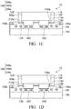
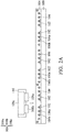
- FIGS. 1C, 1D , 1E, 1F , 1G and 1H are some other embodiments of display devices with a protection layer including one or more organic sub-layers and inorganic sub-layers.
- outermost sidewalls 110a' of the organic sub-layer 110a may be aligned with outermost sidewalls 108' of the light-emitting component 108.
- outermost sidewalls 110a' of the organic sub-layer 110a may retract from the outermost sidewalls 108' of the light-emitting component 108.
- outermost sidewalls 110b' of the inorganic sub-layer 110b may also retract from the outermost sidewalls 108' of the light-emitting component 108.
- the protection layer 110 may further include an innermost inorganic sub-layer 110c, such that the organic sub-layer 110a is interposed between the outermost inorganic sub-layer 110b and the innermost inorganic sub-layer 110c.
- outermost sidewalls 110c' of the inorganic sub-layer 110c may retract from the outermost sidewalls 108' of the light-emitting component 108.
- the outermost sidewalls 110a' of the organic sub-layer 110a, the outermost sidewalls 110b' of the inorganic sub-layer 110b, and the outermost sidewalls 110c' of the inorganic sub-layer 110c are substantially perpendicular to the top surface of the substrate 100 (as shown in FIGS. 1B-1G ).
- the angle between the outermost sidewalls 110a' of the organic sub-layer 110a and the top surface of the substrate 100 may be greater than zero and less than ⁇ , and/or the angle between the outermost sidewalls 110b' of the inorganic sub-layer 110b and the top surface of the substrate 100 may be greater than zero and less than ⁇ , and/or the angle between the outermost sidewalls 110c' of the inorganic sub-layer 110c and the top surface of the substrate 100 may be greater than zero and less than ⁇ .
- At least one of the outermost sidewalls of the sub-layers of the protection layer 110 can taper inwardly in a direction towards the substrate 100.
- the outermost sidewalls 110a' of the organic sub-layer 110a taper inwardly in a direction towards the substrate 100.
- the outermost sidewalls 110a' of the organic sub-layer 110a, the outermost sidewalls 110b' of the inorganic sub-layer 110b, and the outermost sidewalls 110c' of the inorganic sub-layer 110c are substantially straight (as shown in FIGS. 1B-1G ). In other embodiments, at least one of the outermost sidewalls 110a' of the organic sub-layer 110a, the outermost sidewalls 110b' of the inorganic sub-layer 110b, and the outermost sidewalls 110c' of the inorganic sub-layer 110c may be curved.
- the cover plate may be made of glass, indium tin oxide, polyimide, polyethylene terephthalate, other applicable materials, or a combination thereof.
- the optical film may include a diffuser film, a condensing lens, other applicable optical films, or a combination thereof.
- the light-emitting structure which includes the light-emitting component 108 and the protection layer 110 as illustrated in FIGS. 1A-1H are intended to be included within the scope of the present disclosure, and can be used in other embodiments of the preset disclosure (e.g., Embodiments 2-6).
- the protection layer 110 includes the organic sub-layer 110a and the inorganic sub-layer 110b
- the organic sub-layer 110a may be used to support the light-emitting component 108 and prevent the light-emitting component 108 from damage in a transferring process
- the inorganic sub-layer 110b may be used to change the surface properties of the protection layer 110 (e.g., changing the surface properties of the protection layer 110 to prevent moisture or to improve light extraction coefficient).
- Embodiment 2 provides a method for forming display devices of the above embodiments.
- the light-emitting component 108 including a connection feature (e.g., 108a and 108b) is provided.
- the light-emitting component 108 is surrounded or partially surrounded by the protection layer 110.
- the substrate 100 e.g., a thin-film transistor substrate
- the adhesion film 104 containing a plurality of conductive particles 106 is formed on the substrate 100 and the conductive pad 102.
- the conductive particles 106 are randomly distributed in the adhesion film 104.
- a spin-on coating or other applicable method can be used to form the adhesion film 104 on the substrate 100 and the conductive pad 102.
- the bonding process may include a eutectic bonding process.
- the lower portion of the connection feature (e.g., 108a and 108b) of the light-emitting component 108 may include a first metal
- the conductive pad 102 may include a second metal (e.g., an upper portion of the conductive pad 102)
- the plurality of conductive particles 106 may include a third metal (e.g., the shell portion 106b of the conductive particle 106).
- a solid solution or an intermetallic compound of the first metal and the third metal may be formed between the lower portion of the connection feature of the light-emitting component 108 and the plurality of conductive particles 106 by the eutectic bonding process, and a solid solution or an intermetallic compound of the second metal and the third metal may be formed between the conductive pad 102 and the plurality of conductive particles 106 by the eutectic bonding process.
- the adhesion film 104 may be cured by an ultraviolet light.
- the adhesion film 104 may be thermally cured at a temperature higher than (e.g., 50°C higher than) the eutectic reaction temperature of the first metal and the third metal and/or higher than (e.g., 50°C higher than) the eutectic reaction temperature of the second metal and the third metal.
- the adhesion film 104 may be cured by an ultraviolet light or may be cured at a temperature higher than the eutectic reaction temperature of the eutectic bonding process, the adhesion film 104 remains uncured after being subject to the bonding process (e.g., eutectic bonding process). Therefore, if the light-emitting component 108 is abnormal after the bonding process, it still can be removed or replaced with another light-emitting component.
- a plurality of light-emitting components can be bonded to the substrate 100 using the above method.
- a light-emitting component 208 surrounded by a protection layer 210 and a light-emitting component 208' surrounded by a protection layer 210' may be also bonded to the substrate 100.
- the light-emitting component 108, the light-emitting component 208, and the light-emitting component 208' may be light-emitting diodes of different colors.
- the light-emitting component 108 may be a blue light-emitting diode
- the light-emitting component 208 may be a green light-emitting diode
- the light-emitting component 208' may be a red light-emitting diode.
- the adhesion film 104 is formed on the substrate 100 before the bonding process.
- the adhesion film 104 can be formed on the connection feature of the light-emitting component (e.g., light-emitting component 108, 208, or 208') before the bonding process.
- a cover plate or an optical film may also be formed on the substrate 100 to protect the display device or improve its performance.
- Embodiment 3 provides a method for forming a display device by transferring a plurality of light-emitting components to a substrate (e.g., thin-film transistor substrate).
- a substrate e.g., thin-film transistor substrate.
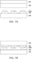
- a first temporary substrate 300 with a first adhesion film 302 thereon is provided.
- the first temporary substrate 300 may be made of glass, polyimide, polyethylene terephthalate, other applicable materials, or a combination thereof.
- the first adhesion film 302 may include a UV-light debondable adhesion film, a heat debondable adhesion film, other applicable adhesion films, or a combination thereof.
- the first adhesion film 302 may be a glue, a tape, or a combination thereof.
- a spin-on coating or other applicable methods can be used to form the first adhesion film 302 on the first temporary substrate 300.
- the first adhesion film 302 may be a patterned adhesion film formed by a lithography process, ink jet, aerosol jet, other applicable processes, or a combination thereof.
- a carrier 304 with a plurality of light-emitting components 306 formed thereon is provided.
- the carrier 304 may include a sapphire substrate, a silicon substrate, a silicon carbide substrate, other applicable carriers, or a combination thereof.
- the light-emitting components 306 may include a light-emitting diode (lateral or vertical), an organic light-emitting diode, other applicable light-emitting components, or a combination thereof.
- the light-emitting component 306 is a light-emitting diode including a connection feature 306a (e.g., a bump or electrode of the light-emitting diode).
- at least one of the light-emitting components 306 on the carrier is partially surrounded by a protection layer (e.g., the protection layer 110 shown in FIGS.1B-1H ).
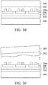
- the plurality of light-emitting components 306 are attached onto the first temporary substrate 300 through the first adhesion film 302.
- the connection feature 306a of the light-emitting component 306 extends into an upper portion of the first adhesion film 302.
- the carrier 304 is removed from the plurality of light-emitting components 306.
- the carrier 304 can be removed by a laser lift-off process, a mechanical peeling, other applicable processes, or a combination thereof.
- the laser source of the laser lift-off process may include an excimer laser, a pico laser, a femto laser, other applicable laser sources, or a combination thereof.
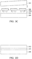
- a second temporary substrate 308 with a light-responsive layer 310 thereon is provided.
- the second temporary substrate 308 may be made of glass, polyimide, polyethylene terephthalate, other applicable materials, or a combination thereof.
- the light-responsive layer 310 may include glue, and particles disposed in the glue.
- the particles of the light-responsive layer 310 can be expanded by a heating process (e.g., a laser heating process).
- the light-responsive layer 310 may be formed on the second temporary substrate 308 by a spin-on coating process, other applicable processes, or a combination thereof.
- a second adhesion film 312 is formed on the light-responsive layer 310 on the second temporary substrate 308.
- the second adhesion film 312 may include a UV-light debondable adhesion film, a heat debondable adhesion film, other applicable adhesion films, or a combination thereof.
- the second adhesion film 312 may be a glue, a tape, or a combination thereof.
- a spin-on coating or other applicable methods can be used to form the second adhesion film 312 on the light-responsive layer 310 on the second temporary substrate 312.
- the second adhesion film 312 may be a patterned adhesion film formed by a lithography process, ink jet, aerosol jet, other applicable processes, or a combination thereof.
- the second adhesion film 312 is a patterned adhesion film including a plurality of adhesive pads (e.g., glue dots), and a pitch of the plurality of adhesive pads (e.g., the distance between the center lines of two adjacent adhesive pads) is an integer multiple of a pitch of the plurality of light-emitting components 306 (e.g., the distance between the center lines of two adjacent light-emitting components 306) on the first temporary substrate 300.
- the second adhesion film 312 may be directly formed on the second temporary substrate 308 (i.e., without forming the light-responsive layer 310 on the second temporary substrate 308), and/or the second adhesion film 312 may be a single-layered or multi-layered structure.
- the first adhesion film 302 on the first temporary substrate 300 can be debonded by a UV-light of a first wavelength
- the second adhesion film 312 on the second temporary substrate 308 can be debonded by a UV-light of a second wavelength that is different from the first wavelength.
- one of the first adhesion film 302 and the second adhesion film 312 is a UV-light debondable film
- the other one of the first adhesion film 302 and the second adhesion film 312 is a heat debondable film.
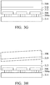
- the plurality of light-emitting components 306 are attached onto the second temporary substrate 308 through the second adhesion film 312, such that the first adhesion film 302 and the second adhesion film 312 are on opposite sides of the light-emitting components 306.
- the first adhesion film 302 and the first temporary substrate 300 are removed from the plurality of light-emitting components 306 by a removal process.
- the removal process may include heating the first adhesion film 302 or exposing the first adhesion film 302 to a UV-light to debond the first adhesion film 302.
- a mechanical peeling may be performed after heating the first adhesion film 302 or exposing the first adhesion film 302 to the UV-light.
- the first adhesion film 302 can be debonded by the UV-light of the first wavelength, and the second adhesion film 312 can be debonded by the UV-light of the second wavelength that is different from the first wavelength.
- the first adhesion film 302 can be debonded by exposing the first adhesion film 302 to the UV-light of the first wavelength, while leaving the second adhesion film 312 substantially undisturbed.
- one of the first adhesion film 302 and the second adhesion film 312 is a UV-light debondable film
- the other one of the first adhesion film and the second adhesion film is a heat debondable film.
- the first adhesion film 302 and the second adhesion film 312 can be debonded by different mechanisms, the first adhesion film 302 can be debonded while leaving the second adhesion film 312 substantially undisturbed.
- the plurality of light-emitting components 306 are bonded onto a substrate 314 (e.g., thin-film transistor substrate).
- the substrate 314 has one or more conductive pads and an adhesion film (e.g., anisotropic conductive film) formed thereon (not shown), and the plurality of light-emitting components 306 may be bonded to the substrate 314 through the adhesion film and the conductive pads by the eutectic bonding process discussed in the above embodiments.
- a filler layer (not shown) may be formed on the substrate 314 before the plurality of light-emitting components 306 are bonded onto the substrate 314, so that the gap between adjacent light-emitting components 306 can be filled by the filler layer.
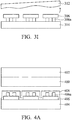
- the second temporary substrate 308, and the light-responsive layer 310 are removed from the second adhesion film 312.
- the light-responsive layer 310 includes particles being able to expand due to a heating process (e.g., a laser heating process), and the expanded particles may be advantageous for removing the second temporary substrate 308 and the light-responsive layer 310 from the second adhesion film 312. Therefore, the step of removing the second temporary substrate 308 and the light-responsive layer 310 from the second adhesion film 312 may include using a laser heating process to heat the particles of the light-responsive layer 310 in some embodiments. In some embodiments, a mechanical peeling may be performed after the heating process.
- the second adhesion film 312 is directly formed on the second temporary substrate 308 (i.e., without forming the light-responsive layer 310 on the second temporary substrate 308), and thus only the second temporary substrate 308 are removed from the second adhesion film 312.
- the second adhesion film 312 is removed from the plurality of light-emitting components 306 by a removal process.
- the removal process may include heating the second adhesion film 312 or exposing the second adhesion film 312 to a UV-light (e.g., a UV-light of the second wavelength) to debond the second adhesion film 312.
- a mechanical peeling may be performed after heating the second adhesion film 312 or exposing the second adhesion film 312 to the UV-light.
- the debonding of the second adhesion film 312 can be improved.
- the debonding of the second adhesion film 312 can be selective (i.e., a portion of the second adhesion film 312 is selectively debonded and another portion of the second adhesion film 312 is not debonded).
- portions of the second adhesion film 312 which correspond to abnormal light-emitting components are not debonded (e.g., not exposed to the UV-light or not heated), and portions of the second adhesion film 312 which correspond to applicable light-emitting components are selectively debonded, such that the abnormal light-emitting components can be removed with the second adhesion film 312 while leaving the applicable light-emitting components on the substrate 314 (e.g., thin-film transistor substrate).
- both the light-responsive layer 310 and the second adhesion film 312 can be debonded by heat.
- the process of removing the second adhesion film 312 can include heating the second adhesion film 312 at a first temperature (e.g., the minimum temperature to debond the second adhesion film 312), and the process of removing the light-responsive layer 310 can include heating the light-responsive layer 310 at a second temperature (e.g., the minimum temperature to debond the light-responsive layer 310) less than the first temperature, such that the second adhesion film 312 are not debonded in the step of removing the light-responsive layer 310.
- a first temperature e.g., the minimum temperature to debond the second adhesion film 312
- a second temperature e.g., the minimum temperature to debond the light-responsive layer 310
- the second adhesion film 312 can be debonded by the UV-light of the second wavelength, and the light-responsive layer 310 can be debonded by a UV-light of a third wavelength different from the second wavelength.
- the light-responsive layer 310 can be debonded by exposing the light-responsive layer 310 to the UV-light of the third wavelength, while leaving the second adhesion film 312 substantially undisturbed.
- one of the light-responsive layer 310 and the second adhesion film 312 is a UV-light debondable film
- the other one of the light-responsive layer 310 and the second adhesion film 312 is a heat debondable film.
- the light-responsive layer 310 can be debonded by the UV-light or heat, while leaving the second adhesion film 312 substantially undisturbed.
- a cover plate or an optical film may also be formed on the substrate 314 to protect the display device or improve its performance.
- Embodiment 4 also provides a method for forming a display device by transferring a plurality of light-emitting components to a substrate (e.g., thin-film transistor substrate).
- a substrate e.g., thin-film transistor substrate.
- One difference between Embodiment 3 and Embodiment 4 is that the light-responsive layer of Embodiment 4 is formed on the light-emitting components on the carrier.
- a first temporary substrate 400 with a first adhesion film 402 thereon is provided.
- the first temporary substrate 400 may be made of glass, polyimide, polyethylene terephthalate, other applicable materials, or a combination thereof.
- the first adhesion film 402 may include a UV-light debondable adhesion film, a heat debondable adhesion film, other applicable adhesion film, or a combination thereof.
- the first adhesion film 402 may be a glue, a tape, or a combination thereof.
- a spin-on coating or other applicable methods can be used to form the first adhesion film 402 on the first temporary substrate 400.
- the first adhesion film 402 may be a patterned adhesion film formed by a lithography process, ink jet, aerosol jet, other applicable processes, or a combination thereof.
- a carrier 404 with a plurality of light-emitting components 406 formed thereon is provided.
- the carrier 404 may include a sapphire substrate, a silicon substrate, a silicon carbide substrate, other applicable carrier, or a combination thereof.
- the light-emitting components 406 may include a light-emitting diode (lateral or vertical), an organic light-emitting diode, other applicable light-emitting components, or a combination thereof.
- the light-emitting component 406 is a light-emitting diode including a connection feature 406a (e.g., a bump or electrode of the light-emitting diode).
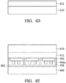
- a light-responsive layer 408 is formed on the carrier 404 and the plurality of light-emitting components 406 by an applicable process (e.g., a spin-on coating process).
- the light-responsive layer 408 is conformally formed on the carrier 404 and the plurality of light-emitting components 406, as shown in FIG. 4A .
- the light-responsive layer 408 may include glue, and particles disposed in the glue.
- the particles of the light-responsive layer 408 can be expanded by a heating process (e.g., a laser heating process).
- the plurality of light-emitting components 406 are attached onto the first temporary substrate 400 through the first adhesion film 402.
- the connection feature 406a of the light-emitting component 406 extends into an upper portion of the first adhesion film 402.
- the carrier 404 is removed from the plurality of light-emitting components 406.
- the carrier 404 can be removed by a laser lift-off process, a mechanical peeling, other applicable processes, or a combination thereof.
- the laser source of the laser lift-off process may include an excimer laser, a pico laser, a femto laser, other applicable laser sources, or a combination thereof.
- a second temporary substrate 410 with a second adhesion film 412 thereon is provided.
- the second temporary substrate 410 may be made of glass, polyimide, polyethylene terephthalate, other applicable materials, or a combination thereof.
- the second adhesion film 412 may include a UV-light debondable adhesion film, a heat debondable adhesion film, other applicable adhesion films, or a combination thereof.
- the second adhesion film 412 may be a glue, a tape, or a combination thereof.
- a spin-on coating or other applicable methods can be used to form the second adhesion film 412 on the second temporary substrate 410.
- the second adhesion film 412 may be a patterned adhesion film formed by a lithography process, ink jet, aerosol jet, other applicable processes, or a combination thereof.
- the plurality of light-emitting components 406 are attached onto the second temporary substrate 410 through the second adhesion film 412, such that the first adhesion film 402 and the second adhesion film 412 are on opposite sides of the light-emitting components 406.
- the first adhesion film 402 and the first temporary substrate 400 are removed from the plurality of light-emitting components 406 by a removal process.
- the light-responsive layer 408 includes particles being able to expand due to a heating process (e.g., a laser heating process), and the expanded particles may be advantageous for removing the first adhesion film 402 and the first temporary substrate 400 from the plurality of light-emitting components 406. Therefore, the step of removing the first adhesion film 402 and the first temporary substrate 400 from the plurality of light-emitting components 406 may include using a laser heating process to heat the particles of the light-responsive layer 408 in some embodiments. In some embodiments, a mechanical peeling may be performed after the heating process.
- the light-responsive layer 408 is removed from the plurality of light-emitting components 406.
- the light-responsive layer 408 can be removed with an organic solution (e.g., Acetone, alcohol, or methyl), an inorganic solution (e.g., Silicone Oil), or a combination thereof.
- the plurality of light-emitting components 406 are bonded onto a substrate 414 (e.g., thin-film transistor substrate).
- the substrate 414 has one or more conductive pads and an adhesion film (e.g., anisotropic conductive film) formed thereon (not shown), and the plurality of light-emitting components 406 may be bonded to the substrate 414 through the adhesion film and the conductive pads by the eutectic bonding process discussed in the above embodiments.
- a filler layer (not shown) may be formed on the substrate 414 before the plurality of light-emitting components 406 are bonded onto the substrate 414, so that the gap between adjacent light-emitting components 406 can be filled by the filler layer.
- the second adhesion film 412 and the second temporary substrate 410 are removed from the plurality of light-emitting components 406 by a removal process.
- the removal process may include heating the second adhesion film 412 or exposing the second adhesion film 412 to a UV-light to debond the second adhesion film 412.
- a mechanical peeling may be performed after heating the second adhesion film 412 or exposing the second adhesion film 412 to the UV-light.
- a cover plate or an optical film may also be formed on the substrate 414 to protect the display device or improve its performance.
- the light-responsive layer 408 may be replaced with a release film.
- the release film may contain halogens.
- a surface treatment may be performed on the plurality of light-emitting components 406 before forming the release film on the plurality of light-emitting components 406.
- hydroxyl groups are formed on the surface of the light-emitting component 406 by the surface treatment.
- Embodiment 5 provides a method for forming a display device by transferring a plurality of light-emitting components to a substrate (e.g., thin-film transistor substrate).
- a substrate e.g., thin-film transistor substrate.
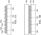
- a first carrier 500 with a first plurality of light-emitting components formed thereon is provided.
- the first plurality of light-emitting components includes a first group of light-emitting components (i.e., 502) and a second group of light-emitting components (i.e., 504).
- the first group of light-emitting components (i.e., 502) and the second group of light-emitting components (i.e., 504) may be alternatively disposed.
- the first carrier 500 may include a sapphire substrate, a silicon substrate, a silicon carbide substrate, other applicable carrier, or a combination thereof.
- the light-emitting components 502 and 504 may include a light-emitting diode (lateral or vertical), an organic light-emitting diode, other applicable light-emitting components, or a combination thereof.
- the light-emitting components 502 and 504 are light-emitting diodes including connection features 502a and 504a (e.g., a bump or electrode of the light-emitting diode).
- at least one of the first plurality of light-emitting components on the first carrier 500 is partially surrounded by a protection layer (e.g., the protection layer 110 shown in FIGS.1B-1H ).
- the first plurality of light-emitting components 502 and 504 are attached onto a first temporary substrate 506 through a first adhesion film 508.
- the first temporary substrate 506 may be made of glass, polyimide, polyethylene terephthalate, other applicable materials, or a combination thereof.
- the first adhesion film 508 may include a UV-light debondable adhesion film, a heat debondable adhesion film, other applicable adhesion film, or a combination thereof.
- the first adhesion film 508 may be a glue, a tape, or a combination thereof.
- a spin-on coating or other applicable method can be used to form the first adhesion film 508 on the first temporary substrate 506 before the first plurality of light-emitting components 502 and 504 are attached onto the first temporary substrate 506.
- the first carrier 500 is removed from the first plurality of light-emitting components 502 and 504.
- the first carrier 500 can be removed by a laser lift-off process, a mechanical peeling, other applicable processes, or a combination thereof.
- the laser source of the laser lift-off process may include an excimer laser, a pico laser, a femto laser, other applicable laser sources, or a combination thereof.
- at least one of the first plurality of light-emitting components on the first temporary substrate 506 is partially surrounded by a protection layer (e.g., the protection layer 110 shown in FIGS.1B-1H ).
- the first plurality of light-emitting components 502 and 504 are disposed on the first temporary substrate 506 at a pitch of Q 1 (e.g., the distance between the center lines of two adjacent light-emitting components of the first plurality of light-emitting components).
- the pitch Q 1 may be 2 to 500 ⁇ m, whose value depends on the size of LED chips.
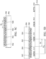
- a first transfer substrate 510 with a first plurality of adhesive pads (e.g., glue dots) thereon is provided.
- the first plurality of adhesive pads includes a first group of adhesive pads (i.e., 512) corresponding to the first group of the first plurality of light-emitting components (i.e., 502) and a second group of adhesive pads (i.e., 514) corresponding to the second group of the first plurality of light-emitting components (i.e., 504).
- a first group of adhesive pads i.e., 512
- second group of adhesive pads i.e., 514
- the first plurality of adhesive pads are disposed on the first transfer substrate 510 at a pitch of Q 2 (e.g., the distance between the center lines of two adjacent adhesive pads of the first plurality of adhesive pads).
- the pitch Q 2 of the first plurality of adhesive pads is an integer multiple of the pitch Q 1 of the first plurality of light-emitting components (e.g., Q 2 is substantially equal to twice Q 1 in the present embodiment).
- the first plurality of adhesive pads may include a thermal plastic material, other applicable material, or a combination thereof.
- the first plurality of adhesive pads can be formed by lithography process, ink jet, aerosol jet, other applicable processes, or a combination thereof.
- the material of the first plurality of adhesive pads can include heat debondable materials and/or UV-light debondable materials.
- the first group of the first plurality of light-emitting components i.e., 502 are attached onto the first group of the first plurality of adhesive pads (i.e., 512) on the first transfer substrate 510 by an attachment process.
- the attachment process compresses the first group of the first plurality of adhesive pads (i.e., 512), so that a thickness of the first group of the first plurality of adhesive pads (i.e., 512) is less than a thickness of the second group of the first plurality of adhesive pads (i.e., 514) after the attachment process (as shown in FIG. 5E ).
- a heating process or another applicable process may be performed on the first group of the first plurality of adhesive pads (i.e., 512) before the attachment process, which may be advantageous to the attachment process by increasing the plasticity of the first group of the first plurality of adhesive pads (i.e., 512).
- the attachment process can selectively attach the first group of the first plurality of light-emitting components (i.e., 502) onto the first transfer substrate 510, while leaving the second group of the first plurality of light-emitting components (i.e., 504) remaining on the first temporary substrate 506.
- the first temporary substrate 506, the first adhesion film 508, and the second group of the first plurality of light-emitting components are removed by a removal process, and the first group of the first plurality of light-emitting components (i.e., 502) are left on the first transfer substrate 510.
- the first adhesion film 508 may be heated or exposed to a UV-light before the removal process, which may be advantageous to the removal process by reducing the bonding force between the adhesion film 508 and the first group of the first plurality of light-emitting components (i.e., 502).
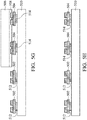
- the second group of the first plurality of light-emitting components i.e., 504 are attached onto the second group of the first plurality of adhesive pads (i.e., 514) on the first transfer substrate 510 by an attachment process similar to the above attachment process for the first group of the first plurality of light-emitting components (i.e., 502).
- the first temporary substrate 506 and the first adhesion film 508 are removed by a removal process, and the second group of the first plurality of light-emitting components (i.e., 504) is left on the first transfer substrate 510.
- the first adhesion film 508 may be heated or exposed to a UV-light before the removal process, which may be advantageous to the attachment process by reducing the bonding force between the adhesion film 508 and the second group of the first plurality of light-emitting components (i.e., 504).
- the first plurality of light-emitting components are bonded onto a substrate 516 (e.g., thin-film transistor substrate).
- the substrate 516 has one or more conductive pads and an adhesion film (e.g., anisotropic conductive film) formed thereon (not shown), and the first plurality of light-emitting components may be bonded to the substrate 516 through the adhesion film and the conductive pads by the eutectic bonding process discussed in the above embodiments.
- the first transfer substrate 510 and the first plurality of adhesive pads are removed from the first plurality of light-emitting components (i.e., 502 and 504) by a removal process.
- the removal process may include heating the first plurality of adhesive pads, exposing the first plurality of adhesive pads to a UV-light, a laser lift off process, another applicable process, or a combination thereof.
- a cover plate or an optical film may also be formed on the substrate 516 to protect the display device or improve its performance.
- a filler layer 518 may be formed on the substrate 516 before the first plurality of light-emitting components (i.e., 502 and 504) are bonded onto the substrate 516, so that the gap between adjacent light-emitting components can be filled by the filler layer (as shown in FIG. 5K ).
- a curing process may be performed to cure the filler layer 518 after the first plurality of light-emitting components (i.e., 502 and 504) are bonded onto the substrate 516.
- the filler layer 518 may include glass, polyimide, flux, micro/nano particles, other applicable materials, or a combination thereof.
- the first transfer substrate 510 may not be removed after the first plurality of light-emitting components (i.e., 502 and 504) are bonded onto the substrate 516 (as shown in FIG. 5L ). In such embodiments, the first transfer substrate 510 may provide the display device with some advantageous functions (e.g., mechanical protection or optical conversion).
- the first plurality of adhesive pads are formed by ink jet or aerosol jet after performing a testing process to test the quality of the first plurality of light-emitting components (i.e., 502 and 504), and thus the pattern of the first plurality of adhesive pads can be adjusted according to the test results to avoid the abnormal light-emitting components being transferred to the first transfer substrate 510.
- the first plurality of adhesive pads are formed by ink jet or aerosol jet before or after performing a testing process to test the quality of the first plurality of light-emitting components (i.e., 502 and 504), and some of the first plurality of adhesive pads corresponding to the light-emitting components having abnormal quality (e.g., according to the test results) may be removed by a removal process (e.g., a laser process) before the attachment process to avoid the abnormal light-emitting components being transferred to the first transfer substrate 510.
- a removal process e.g., a laser process
- Embodiment 6 provides a method for forming a display device.
- One difference between Embodiment 5 and Embodiment 6 is that two or more transfer substrates are used in Embodiment 6.
- a first transfer substrate 600 with a first plurality of light-emitting components 604 formed thereon is provided.
- the first plurality of light-emitting components 604 are attached onto the first transfer substrate 600 through a first plurality of adhesive pads 602.
- the first plurality of adhesive pads 602 have a pitch of M 1 , which may be substantially equal to a pitch of the first plurality of light-emitting components 604 on the first transfer substrate 600.
- a second transfer substrate 606 with a second plurality of light-emitting components 610 formed thereon is also provided.
- the second plurality of light-emitting components 610 are attached onto the second transfer substrate 606 through a second plurality of adhesive pads 608.
- the second plurality of adhesive pads 608 have a pitch of M 2 , which may be substantially equal to a pitch of the second plurality of light-emitting components 608 on the second transfer substrate 606.
- a third transfer substrate 612 with a third plurality of light-emitting components 616 formed thereon is also provided.
- the third plurality of light-emitting components 616 are attached onto the third transfer substrate 612 through a third plurality of adhesive pads 614.
- the third plurality of adhesive pads 614 have a pitch of M 3 , which may be substantially equal to a pitch of the third plurality of light-emitting components 616 on the third transfer substrate 612.
- the transfer substrates, the adhesive pads and the light-emitting components of the present embodiment may be the same as, or similar to, the above embodiments, and may be formed using the same or similar methods as disclosed in the above embodiments.
- the pitch M 1 of the first plurality of adhesive pads 602, the pitch M 2 of the second plurality of adhesive pads 608, and the pitch M 3 of the third plurality of adhesive pads 614 may be substantially the same.
- the first plurality of light-emitting components 604 includes light-emitting diodes of a first color
- the second plurality of light-emitting components 610 includes light-emitting diodes of a second color
- the third plurality of light-emitting components 616 includes light-emitting diodes of third color.
- the first color, the second color, and the third color are different from each other, and are selected from red, green, and blue.
- a bonding process is performed to bond the first plurality of light-emitting components 604 onto a substrate 618 (e.g., thin-film transistor substrate). Then, the first transfer substrate 600 and the first plurality of adhesive pads 602 are removed from the first plurality of light-emitting components 604.
- a substrate 618 e.g., thin-film transistor substrate
- FIG. 6D another bonding process is performed to bond the third plurality of light-emitting components 616 onto the substrate 618. Then, the third transfer substrate 612 and the third plurality of adhesive pads 614 are removed from the third plurality of light-emitting components 616.
- the pitch M 1 of the first plurality of adhesive pads 602, the pitch M 2 of the second plurality of adhesive pads 608, and the pitch M 3 of the third plurality of adhesive pads 614 may respectively be an integer multiple of a pitch N 1 (as shown in FIG. 6D ) of the light-emitting components transferred to the substrate 618 (i.e., 604, 610, and 616).
- the pitch M 1 may is substantially three times the pitch N 1 in the present embodiment.
- a cover plate or an optical film may also be formed on the substrate 618 to protect the display device or improve its performance.
- a filler layer (not shown) may be formed on the substrate 618 before the light-emitting components (i.e., 604, 610, and 616) are bonded onto the substrate 618, so that the gap between adjacent light-emitting components can be filled by the filler layer.
- a curing process may be performed to cure the filler layer after the light-emitting components (i.e., 604, 610, and 616) are bonded onto the substrate 618.
- the filler layer may include glass, polyimide, other applicable materials, or a combination thereof.
- a method for forming a display device comprising:
- Embodiment A further comprising:
- Embodiment A or Embodiment B further comprising:
- the first plurality of light-emitting components comprises a first plurality of light-emitting diodes of a first color
- the second plurality of light-emitting components comprises a second plurality of light-emitting diodes of a second color different from the first color
- the first plurality of adhesive pads comprise a UV-light debondable material or a heat debondable material.
- a light-emitting structure comprising:
- the protection layer further comprises another inorganic sub-layer, and the organic sub-layer is interposed between the inorganic sub-layer and the another inorganic sub-layer.
Landscapes
- Physics & Mathematics (AREA)
- General Physics & Mathematics (AREA)
- Engineering & Computer Science (AREA)
- Theoretical Computer Science (AREA)
- Electroluminescent Light Sources (AREA)
- Devices For Indicating Variable Information By Combining Individual Elements (AREA)
Applications Claiming Priority (3)
| Application Number | Priority Date | Filing Date | Title |
|---|---|---|---|
| US201762441579P | 2017-01-03 | 2017-01-03 | |
| US201762465869P | 2017-03-02 | 2017-03-02 | |
| US15/659,947 US10483434B2 (en) | 2017-01-03 | 2017-07-26 | Display devices and methods for forming display devices |
Publications (3)
| Publication Number | Publication Date |
|---|---|
| EP3352217A2 true EP3352217A2 (de) | 2018-07-25 |
| EP3352217A3 EP3352217A3 (de) | 2018-11-07 |
| EP3352217B1 EP3352217B1 (de) | 2021-06-02 |
Family
ID=60888211
Family Applications (1)
| Application Number | Title | Priority Date | Filing Date |
|---|---|---|---|
| EP17209569.7A Active EP3352217B1 (de) | 2017-01-03 | 2017-12-21 | Anzeigevorrichtung |
Country Status (4)
| Country | Link |
|---|---|
| US (2) | US10483434B2 (de) |
| EP (1) | EP3352217B1 (de) |
| KR (1) | KR102540517B1 (de) |
| CN (2) | CN115360189A (de) |
Cited By (4)
| Publication number | Priority date | Publication date | Assignee | Title |
|---|---|---|---|---|
| EP3460861A3 (de) * | 2017-09-21 | 2019-07-03 | InnoLux Corporation | Anzeigevorrichtung |
| WO2020242053A1 (en) | 2019-05-28 | 2020-12-03 | Samsung Electronics Co., Ltd. | Display apparatus, source substrate structure, driving substrate structure, and method of manufacturing display apparatus |
| EP3844818A4 (de) * | 2019-05-28 | 2021-12-01 | Samsung Electronics Co., Ltd. | Anzeigevorrichtung, quellensubstratstruktur, antriebssubstratstruktur und verfahren zur herstellung einer anzeigevorrichtung |
| EP4084068A4 (de) * | 2019-12-24 | 2024-01-24 | Seoul Viosys Co., Ltd | Verfahren zum wiederherstellen einer lichtemittierenden vorrichtung, gerät zum wiederherstellen einer lichtemittierenden vorrichtung und anzeigetafel, die eine wiederhergestellte lichtemittierende vorrichtung umfasst |
Families Citing this family (28)
| Publication number | Priority date | Publication date | Assignee | Title |
|---|---|---|---|---|
| US10886250B2 (en) | 2015-07-10 | 2021-01-05 | Invensas Corporation | Structures and methods for low temperature bonding using nanoparticles |
| WO2017146477A1 (ko) | 2016-02-26 | 2017-08-31 | 서울반도체주식회사 | 디스플레이 장치 및 그의 제조 방법 |
| TWI822659B (zh) | 2016-10-27 | 2023-11-21 | 美商艾德亞半導體科技有限責任公司 | 用於低溫接合的結構和方法 |
| WO2018191551A1 (en) * | 2017-04-13 | 2018-10-18 | Hong Kong Beida Jade Bird Display Limited | Led-oled hybrid self-emissive display |
| US20190044023A1 (en) * | 2017-08-01 | 2019-02-07 | Innolux Corporation | Methods for manufacturing semiconductor device |
| US20190181122A1 (en) * | 2017-12-13 | 2019-06-13 | Innolux Corporation | Electronic device and method of manufacturing the same |
| TWI706554B (zh) * | 2017-12-13 | 2020-10-01 | 友達光電股份有限公司 | 畫素陣列基板及其製造方法 |
| DE112018006965T5 (de) * | 2018-01-29 | 2020-10-08 | Lg Electronics Inc. | Verfahren zur Herstellung einer Anzeigevorrichtung unter Verwendung lichtemittierender Halbleiterelemente und Anzeigevorrichtung |
| CN109461805B (zh) | 2018-03-07 | 2021-08-10 | 普瑞光电股份有限公司 | 具有位于包含荧光体的玻璃转换板上的玻璃透镜的汽车led光源 |
| JP7084228B2 (ja) * | 2018-06-26 | 2022-06-14 | 日東電工株式会社 | 半導体装置製造方法 |
| US11127720B2 (en) | 2019-01-21 | 2021-09-21 | Nanosys, Inc. | Pixel repair method for a direct view display device |
| US11424224B2 (en) * | 2019-04-24 | 2022-08-23 | Seoul Viosys Co., Ltd. | LED display panel, LED display apparatus having the same and method of fabricating the same |
| KR102723703B1 (ko) * | 2019-05-28 | 2024-10-31 | 삼성디스플레이 주식회사 | 표시 장치 및 표시 장치 제조 방법 |
| EP3985744B1 (de) * | 2019-06-13 | 2025-05-21 | BOE Technology Group Co., Ltd. | Massentransferverfahren für leuchtdioden |
| KR20200145985A (ko) * | 2019-06-21 | 2020-12-31 | 삼성디스플레이 주식회사 | 표시 장치 및 표시 장치의 제조 방법 |
| KR102802033B1 (ko) * | 2019-10-15 | 2025-04-30 | 삼성전자주식회사 | 디스플레이 장치의 제조 방법, 중계 기판 및 기록 매체에 저장된 컴퓨터 프로그램 |
| CN111244126B (zh) * | 2020-01-20 | 2022-07-12 | 深圳市华星光电半导体显示技术有限公司 | 一种微型显示面板、制程方法及拼接显示面板 |
| WO2021168615A1 (zh) * | 2020-02-24 | 2021-09-02 | 重庆康佳光电技术研究院有限公司 | 发光二极管的巨量转移方法、以及显示背板组件 |
| DE102020202425A1 (de) | 2020-02-26 | 2021-08-26 | OSRAM Opto Semiconductors Gesellschaft mit beschränkter Haftung | Verfahren zur herstellung einer optoelektronischen vorrichtung und optoelektronische vorrichtung |
| WO2022020946A1 (en) * | 2020-07-27 | 2022-02-03 | Vuereal Inc. | Hybrid release layer for microdevice cartridge |
| JP7245889B2 (ja) * | 2020-11-17 | 2023-03-24 | エルジー ディスプレイ カンパニー リミテッド | 表示装置 |
| CN112670311B (zh) * | 2020-12-22 | 2023-07-25 | 业成科技(成都)有限公司 | 微发光二极体显示面板及其制作方法 |
| CN116848631A (zh) | 2020-12-30 | 2023-10-03 | 美商艾德亚半导体接合科技有限公司 | 具有导电特征的结构及其形成方法 |
| TWI747697B (zh) | 2021-01-05 | 2021-11-21 | 錼創顯示科技股份有限公司 | 半導體結構、顯示面板及電子元件模組的製造方法 |
| CN112864146B (zh) * | 2021-01-05 | 2023-04-18 | 錼创显示科技股份有限公司 | 半导体结构、显示面板及电子元件模块的制造方法 |
| EP4033521A1 (de) * | 2021-01-26 | 2022-07-27 | Infineon Technologies AG | Verfahren zum waferbonden und halbleiterbauelementverbund |
| WO2022174425A1 (zh) * | 2021-02-20 | 2022-08-25 | 厦门三安光电有限公司 | 一种微发光元件、微发光阵列、转移方法及其显示器 |
| KR20230134656A (ko) * | 2022-03-14 | 2023-09-22 | 삼성디스플레이 주식회사 | 이방성 도전 필름 및 이를 포함하는 표시 장치 |
Family Cites Families (20)
| Publication number | Priority date | Publication date | Assignee | Title |
|---|---|---|---|---|
| US6965361B1 (en) | 1998-06-16 | 2005-11-15 | Agilent Technologies, Inc. | Method of manufacture of active matrix addressed polymer LED display |
| CN1239048C (zh) | 2003-03-03 | 2006-01-25 | 友达光电股份有限公司 | 显示器 |
| US9000461B2 (en) | 2003-07-04 | 2015-04-07 | Epistar Corporation | Optoelectronic element and manufacturing method thereof |
| JP2006032779A (ja) * | 2004-07-20 | 2006-02-02 | Sanyo Electric Co Ltd | 窒化物半導体発光素子 |
| JP5282431B2 (ja) | 2008-03-31 | 2013-09-04 | 富士通株式会社 | 回路基板及びその製造方法 |
| CN101256998B (zh) * | 2008-04-10 | 2010-06-16 | 日月光半导体制造股份有限公司 | 利用各向异性导电胶层的半导体装置及其制造方法 |
| JP2010251360A (ja) * | 2009-04-10 | 2010-11-04 | Sony Corp | 表示装置の製造方法および表示装置 |
| US9754835B2 (en) * | 2010-02-16 | 2017-09-05 | Deca Technologies Inc. | Semiconductor device and method comprising redistribution layers |
| KR101824034B1 (ko) | 2011-05-24 | 2018-01-31 | 엘지이노텍 주식회사 | 발광 소자 패키지 |
| US8896010B2 (en) | 2012-01-24 | 2014-11-25 | Cooledge Lighting Inc. | Wafer-level flip chip device packages and related methods |
| US8877561B2 (en) | 2012-06-07 | 2014-11-04 | Cooledge Lighting Inc. | Methods of fabricating wafer-level flip chip device packages |
| WO2014140796A1 (en) | 2013-03-15 | 2014-09-18 | Cooledge Lighting, Inc. | Wafer-level flip chip device packages and related methods |
| KR102135352B1 (ko) | 2013-08-20 | 2020-07-17 | 엘지전자 주식회사 | 표시장치 |
| JP6209949B2 (ja) * | 2013-11-13 | 2017-10-11 | 日亜化学工業株式会社 | 発光装置及び発光装置の製造方法 |
| US9812625B2 (en) | 2014-02-18 | 2017-11-07 | Nichia Corporation | Light-emitting device having resin member with conductive particles |
| KR20150098258A (ko) * | 2014-02-19 | 2015-08-28 | 삼성디스플레이 주식회사 | 유기 발광 표시 장치 및 이의 제조 방법 |
| US9679785B2 (en) * | 2015-07-27 | 2017-06-13 | Semtech Corporation | Semiconductor device and method of encapsulating semiconductor die |
| JP2018515942A (ja) * | 2015-10-20 | 2018-06-14 | ゴルテック インコーポレイテッド | マイクロ発光ダイオードの搬送方法、製造方法、装置及び電子機器 |
| KR102593532B1 (ko) * | 2016-06-03 | 2023-10-26 | 삼성디스플레이 주식회사 | 이방성 도전 필름 및 이를 이용한 디스플레이 장치 |
| KR102589214B1 (ko) * | 2016-06-03 | 2023-10-13 | 삼성디스플레이 주식회사 | 표시 장치 |
-
2017
- 2017-07-26 US US15/659,947 patent/US10483434B2/en active Active
- 2017-12-21 EP EP17209569.7A patent/EP3352217B1/de active Active
- 2017-12-27 KR KR1020170180945A patent/KR102540517B1/ko active Active
- 2017-12-29 CN CN202211042506.XA patent/CN115360189A/zh active Pending
- 2017-12-29 CN CN201711472089.1A patent/CN108269798A/zh active Pending
-
2019
- 2019-09-25 US US16/581,939 patent/US10720553B2/en active Active
Non-Patent Citations (1)
| Title |
|---|
| None |
Cited By (5)
| Publication number | Priority date | Publication date | Assignee | Title |
|---|---|---|---|---|
| EP3460861A3 (de) * | 2017-09-21 | 2019-07-03 | InnoLux Corporation | Anzeigevorrichtung |
| WO2020242053A1 (en) | 2019-05-28 | 2020-12-03 | Samsung Electronics Co., Ltd. | Display apparatus, source substrate structure, driving substrate structure, and method of manufacturing display apparatus |
| EP3844818A4 (de) * | 2019-05-28 | 2021-12-01 | Samsung Electronics Co., Ltd. | Anzeigevorrichtung, quellensubstratstruktur, antriebssubstratstruktur und verfahren zur herstellung einer anzeigevorrichtung |
| US11404607B2 (en) | 2019-05-28 | 2022-08-02 | Samsung Electronics Co.. Ltd. | Display apparatus, source substrate structure, driving substrate structure, and method of manufacturing display apparatus |
| EP4084068A4 (de) * | 2019-12-24 | 2024-01-24 | Seoul Viosys Co., Ltd | Verfahren zum wiederherstellen einer lichtemittierenden vorrichtung, gerät zum wiederherstellen einer lichtemittierenden vorrichtung und anzeigetafel, die eine wiederhergestellte lichtemittierende vorrichtung umfasst |
Also Published As
| Publication number | Publication date |
|---|---|
| US20200020831A1 (en) | 2020-01-16 |
| EP3352217B1 (de) | 2021-06-02 |
| CN108269798A (zh) | 2018-07-10 |
| US10483434B2 (en) | 2019-11-19 |
| CN115360189A (zh) | 2022-11-18 |
| EP3352217A3 (de) | 2018-11-07 |
| KR20180080113A (ko) | 2018-07-11 |
| KR102540517B1 (ko) | 2023-06-05 |
| US20180190876A1 (en) | 2018-07-05 |
| US10720553B2 (en) | 2020-07-21 |
Similar Documents
| Publication | Publication Date | Title |
|---|---|---|
| US10720553B2 (en) | Display devices and methods for forming display devices | |
| CN113629097B (zh) | 显示设备及其形成方法 | |
| US9647188B2 (en) | Wafer-level flip chip device packages and related methods | |
| US20150303355A1 (en) | Semiconductor light emitting device and method for manufacturing same | |
| CN113421839A (zh) | 微发光二极管转移方法及制造方法 | |
| CN113345829A (zh) | 微型发光二极管的巨量转移方法、显示装置及其制作方法 | |
| EP2689458B1 (de) | Gemusterte uv-empfindliche silikonphosphorschicht über leds und verfahren zur herstellung derselben | |
| CN108022945A (zh) | 显示装置及其形成方法 | |
| TW201227937A (en) | Image sensor chip package and method for forming the same | |
| US10749076B2 (en) | Light-emitting device | |
| US10546842B2 (en) | Display device and method for forming the same | |
| CN102382585B (zh) | 倒装芯片型半导体背面用膜、半导体背面用条状膜的生产方法和倒装芯片型半导体器件 | |
| WO2020087815A1 (zh) | 一种微型元件的批量转移方法 | |
| JP6447018B2 (ja) | 発光装置及び発光装置の製造方法 | |
| CN114787997A (zh) | 形成多色磷光体转换led阵列 | |
| JP6760356B2 (ja) | 発光装置及び発光装置の製造方法 | |
| US20230117490A1 (en) | Semiconductor element arrangement structure | |
| KR101490799B1 (ko) | 웨이퍼레벨 패키지 구조체, 이를 이용한 led 및 이의 제조방법 | |
| CN118367084B (zh) | 一种MiP芯片及其制备方法 | |
| US20240128414A1 (en) | Light-emitting device |
Legal Events
| Date | Code | Title | Description |
|---|---|---|---|
| PUAI | Public reference made under article 153(3) epc to a published international application that has entered the european phase |
Free format text: ORIGINAL CODE: 0009012 |
|
| STAA | Information on the status of an ep patent application or granted ep patent |
Free format text: STATUS: THE APPLICATION HAS BEEN PUBLISHED |
|
| AK | Designated contracting states |
Kind code of ref document: A2 Designated state(s): AL AT BE BG CH CY CZ DE DK EE ES FI FR GB GR HR HU IE IS IT LI LT LU LV MC MK MT NL NO PL PT RO RS SE SI SK SM TR |
|
| AX | Request for extension of the european patent |
Extension state: BA ME |
|
| PUAL | Search report despatched |
Free format text: ORIGINAL CODE: 0009013 |
|
| AK | Designated contracting states |
Kind code of ref document: A3 Designated state(s): AL AT BE BG CH CY CZ DE DK EE ES FI FR GB GR HR HU IE IS IT LI LT LU LV MC MK MT NL NO PL PT RO RS SE SI SK SM TR |
|
| AX | Request for extension of the european patent |
Extension state: BA ME |
|
| RIC1 | Information provided on ipc code assigned before grant |
Ipc: H01L 33/44 20100101ALI20181002BHEP Ipc: H01L 33/62 20100101ALI20181002BHEP Ipc: H01L 25/075 20060101AFI20181002BHEP |
|
| STAA | Information on the status of an ep patent application or granted ep patent |
Free format text: STATUS: REQUEST FOR EXAMINATION WAS MADE |
|
| 17P | Request for examination filed |
Effective date: 20190502 |
|
| RBV | Designated contracting states (corrected) |
Designated state(s): AL AT BE BG CH CY CZ DE DK EE ES FI FR GB GR HR HU IE IS IT LI LT LU LV MC MK MT NL NO PL PT RO RS SE SI SK SM TR |
|
| STAA | Information on the status of an ep patent application or granted ep patent |
Free format text: STATUS: EXAMINATION IS IN PROGRESS |
|
| 17Q | First examination report despatched |
Effective date: 20200716 |
|
| GRAP | Despatch of communication of intention to grant a patent |
Free format text: ORIGINAL CODE: EPIDOSNIGR1 |
|
| STAA | Information on the status of an ep patent application or granted ep patent |
Free format text: STATUS: GRANT OF PATENT IS INTENDED |
|
| RIC1 | Information provided on ipc code assigned before grant |
Ipc: H01L 25/16 20060101ALI20201126BHEP Ipc: H01L 25/075 20060101AFI20201126BHEP Ipc: H01L 33/62 20100101ALI20201126BHEP Ipc: H01L 33/44 20100101ALI20201126BHEP |
|
| INTG | Intention to grant announced |
Effective date: 20201223 |
|
| GRAS | Grant fee paid |
Free format text: ORIGINAL CODE: EPIDOSNIGR3 |
|
| GRAA | (expected) grant |
Free format text: ORIGINAL CODE: 0009210 |
|
| STAA | Information on the status of an ep patent application or granted ep patent |
Free format text: STATUS: THE PATENT HAS BEEN GRANTED |
|
| REG | Reference to a national code |
Ref country code: CH Ref legal event code: EP |
|
| AK | Designated contracting states |
Kind code of ref document: B1 Designated state(s): AL AT BE BG CH CY CZ DE DK EE ES FI FR GB GR HR HU IE IS IT LI LT LU LV MC MK MT NL NO PL PT RO RS SE SI SK SM TR |
|
| REG | Reference to a national code |
Ref country code: GB Ref legal event code: FG4D |
|
| REG | Reference to a national code |
Ref country code: AT Ref legal event code: REF Ref document number: 1399239 Country of ref document: AT Kind code of ref document: T Effective date: 20210615 |
|
| REG | Reference to a national code |
Ref country code: IE Ref legal event code: FG4D |
|
| REG | Reference to a national code |
Ref country code: DE Ref legal event code: R096 Ref document number: 602017039603 Country of ref document: DE |
|
| REG | Reference to a national code |
Ref country code: LT Ref legal event code: MG9D |
|
| PG25 | Lapsed in a contracting state [announced via postgrant information from national office to epo] |
Ref country code: FI Free format text: LAPSE BECAUSE OF FAILURE TO SUBMIT A TRANSLATION OF THE DESCRIPTION OR TO PAY THE FEE WITHIN THE PRESCRIBED TIME-LIMIT Effective date: 20210602 Ref country code: LT Free format text: LAPSE BECAUSE OF FAILURE TO SUBMIT A TRANSLATION OF THE DESCRIPTION OR TO PAY THE FEE WITHIN THE PRESCRIBED TIME-LIMIT Effective date: 20210602 Ref country code: HR Free format text: LAPSE BECAUSE OF FAILURE TO SUBMIT A TRANSLATION OF THE DESCRIPTION OR TO PAY THE FEE WITHIN THE PRESCRIBED TIME-LIMIT Effective date: 20210602 Ref country code: BG Free format text: LAPSE BECAUSE OF FAILURE TO SUBMIT A TRANSLATION OF THE DESCRIPTION OR TO PAY THE FEE WITHIN THE PRESCRIBED TIME-LIMIT Effective date: 20210902 |
|
| REG | Reference to a national code |
Ref country code: NL Ref legal event code: MP Effective date: 20210602 |
|
| REG | Reference to a national code |
Ref country code: AT Ref legal event code: MK05 Ref document number: 1399239 Country of ref document: AT Kind code of ref document: T Effective date: 20210602 |
|
| PG25 | Lapsed in a contracting state [announced via postgrant information from national office to epo] |
Ref country code: SE Free format text: LAPSE BECAUSE OF FAILURE TO SUBMIT A TRANSLATION OF THE DESCRIPTION OR TO PAY THE FEE WITHIN THE PRESCRIBED TIME-LIMIT Effective date: 20210602 Ref country code: RS Free format text: LAPSE BECAUSE OF FAILURE TO SUBMIT A TRANSLATION OF THE DESCRIPTION OR TO PAY THE FEE WITHIN THE PRESCRIBED TIME-LIMIT Effective date: 20210602 Ref country code: NO Free format text: LAPSE BECAUSE OF FAILURE TO SUBMIT A TRANSLATION OF THE DESCRIPTION OR TO PAY THE FEE WITHIN THE PRESCRIBED TIME-LIMIT Effective date: 20210902 Ref country code: PL Free format text: LAPSE BECAUSE OF FAILURE TO SUBMIT A TRANSLATION OF THE DESCRIPTION OR TO PAY THE FEE WITHIN THE PRESCRIBED TIME-LIMIT Effective date: 20210602 Ref country code: GR Free format text: LAPSE BECAUSE OF FAILURE TO SUBMIT A TRANSLATION OF THE DESCRIPTION OR TO PAY THE FEE WITHIN THE PRESCRIBED TIME-LIMIT Effective date: 20210903 Ref country code: LV Free format text: LAPSE BECAUSE OF FAILURE TO SUBMIT A TRANSLATION OF THE DESCRIPTION OR TO PAY THE FEE WITHIN THE PRESCRIBED TIME-LIMIT Effective date: 20210602 |
|
| PG25 | Lapsed in a contracting state [announced via postgrant information from national office to epo] |
Ref country code: NL Free format text: LAPSE BECAUSE OF FAILURE TO SUBMIT A TRANSLATION OF THE DESCRIPTION OR TO PAY THE FEE WITHIN THE PRESCRIBED TIME-LIMIT Effective date: 20210602 Ref country code: RO Free format text: LAPSE BECAUSE OF FAILURE TO SUBMIT A TRANSLATION OF THE DESCRIPTION OR TO PAY THE FEE WITHIN THE PRESCRIBED TIME-LIMIT Effective date: 20210602 Ref country code: PT Free format text: LAPSE BECAUSE OF FAILURE TO SUBMIT A TRANSLATION OF THE DESCRIPTION OR TO PAY THE FEE WITHIN THE PRESCRIBED TIME-LIMIT Effective date: 20211004 Ref country code: ES Free format text: LAPSE BECAUSE OF FAILURE TO SUBMIT A TRANSLATION OF THE DESCRIPTION OR TO PAY THE FEE WITHIN THE PRESCRIBED TIME-LIMIT Effective date: 20210602 Ref country code: AT Free format text: LAPSE BECAUSE OF FAILURE TO SUBMIT A TRANSLATION OF THE DESCRIPTION OR TO PAY THE FEE WITHIN THE PRESCRIBED TIME-LIMIT Effective date: 20210602 Ref country code: EE Free format text: LAPSE BECAUSE OF FAILURE TO SUBMIT A TRANSLATION OF THE DESCRIPTION OR TO PAY THE FEE WITHIN THE PRESCRIBED TIME-LIMIT Effective date: 20210602 Ref country code: CZ Free format text: LAPSE BECAUSE OF FAILURE TO SUBMIT A TRANSLATION OF THE DESCRIPTION OR TO PAY THE FEE WITHIN THE PRESCRIBED TIME-LIMIT Effective date: 20210602 Ref country code: SM Free format text: LAPSE BECAUSE OF FAILURE TO SUBMIT A TRANSLATION OF THE DESCRIPTION OR TO PAY THE FEE WITHIN THE PRESCRIBED TIME-LIMIT Effective date: 20210602 Ref country code: SK Free format text: LAPSE BECAUSE OF FAILURE TO SUBMIT A TRANSLATION OF THE DESCRIPTION OR TO PAY THE FEE WITHIN THE PRESCRIBED TIME-LIMIT Effective date: 20210602 |
|
| REG | Reference to a national code |
Ref country code: DE Ref legal event code: R097 Ref document number: 602017039603 Country of ref document: DE |
|
| PLBE | No opposition filed within time limit |
Free format text: ORIGINAL CODE: 0009261 |
|
| STAA | Information on the status of an ep patent application or granted ep patent |
Free format text: STATUS: NO OPPOSITION FILED WITHIN TIME LIMIT |
|
| PG25 | Lapsed in a contracting state [announced via postgrant information from national office to epo] |
Ref country code: DK Free format text: LAPSE BECAUSE OF FAILURE TO SUBMIT A TRANSLATION OF THE DESCRIPTION OR TO PAY THE FEE WITHIN THE PRESCRIBED TIME-LIMIT Effective date: 20210602 |
|
| 26N | No opposition filed |
Effective date: 20220303 |
|
| PG25 | Lapsed in a contracting state [announced via postgrant information from national office to epo] |
Ref country code: AL Free format text: LAPSE BECAUSE OF FAILURE TO SUBMIT A TRANSLATION OF THE DESCRIPTION OR TO PAY THE FEE WITHIN THE PRESCRIBED TIME-LIMIT Effective date: 20210602 |
|
| PG25 | Lapsed in a contracting state [announced via postgrant information from national office to epo] |
Ref country code: MC Free format text: LAPSE BECAUSE OF FAILURE TO SUBMIT A TRANSLATION OF THE DESCRIPTION OR TO PAY THE FEE WITHIN THE PRESCRIBED TIME-LIMIT Effective date: 20210602 Ref country code: IT Free format text: LAPSE BECAUSE OF FAILURE TO SUBMIT A TRANSLATION OF THE DESCRIPTION OR TO PAY THE FEE WITHIN THE PRESCRIBED TIME-LIMIT Effective date: 20210602 |
|
| REG | Reference to a national code |
Ref country code: CH Ref legal event code: PL |
|
| REG | Reference to a national code |
Ref country code: BE Ref legal event code: MM Effective date: 20211231 |
|
| PG25 | Lapsed in a contracting state [announced via postgrant information from national office to epo] |
Ref country code: LU Free format text: LAPSE BECAUSE OF NON-PAYMENT OF DUE FEES Effective date: 20211221 Ref country code: IE Free format text: LAPSE BECAUSE OF NON-PAYMENT OF DUE FEES Effective date: 20211221 |
|
| PG25 | Lapsed in a contracting state [announced via postgrant information from national office to epo] |
Ref country code: BE Free format text: LAPSE BECAUSE OF NON-PAYMENT OF DUE FEES Effective date: 20211231 |
|
| PG25 | Lapsed in a contracting state [announced via postgrant information from national office to epo] |
Ref country code: LI Free format text: LAPSE BECAUSE OF NON-PAYMENT OF DUE FEES Effective date: 20211231 Ref country code: CH Free format text: LAPSE BECAUSE OF NON-PAYMENT OF DUE FEES Effective date: 20211231 |
|
| PG25 | Lapsed in a contracting state [announced via postgrant information from national office to epo] |
Ref country code: HU Free format text: LAPSE BECAUSE OF FAILURE TO SUBMIT A TRANSLATION OF THE DESCRIPTION OR TO PAY THE FEE WITHIN THE PRESCRIBED TIME-LIMIT; INVALID AB INITIO Effective date: 20171221 |
|
| PG25 | Lapsed in a contracting state [announced via postgrant information from national office to epo] |
Ref country code: CY Free format text: LAPSE BECAUSE OF FAILURE TO SUBMIT A TRANSLATION OF THE DESCRIPTION OR TO PAY THE FEE WITHIN THE PRESCRIBED TIME-LIMIT Effective date: 20210602 |
|
| PG25 | Lapsed in a contracting state [announced via postgrant information from national office to epo] |
Ref country code: MK Free format text: LAPSE BECAUSE OF FAILURE TO SUBMIT A TRANSLATION OF THE DESCRIPTION OR TO PAY THE FEE WITHIN THE PRESCRIBED TIME-LIMIT Effective date: 20210602 |
|
| PG25 | Lapsed in a contracting state [announced via postgrant information from national office to epo] |
Ref country code: MT Free format text: LAPSE BECAUSE OF FAILURE TO SUBMIT A TRANSLATION OF THE DESCRIPTION OR TO PAY THE FEE WITHIN THE PRESCRIBED TIME-LIMIT Effective date: 20210602 |
|
| REG | Reference to a national code |
Ref country code: DE Ref legal event code: R079 Ref document number: 602017039603 Country of ref document: DE Free format text: PREVIOUS MAIN CLASS: H01L0025075000 Ipc: H10H0029240000 |
|
| PG25 | Lapsed in a contracting state [announced via postgrant information from national office to epo] |
Ref country code: TR Free format text: LAPSE BECAUSE OF FAILURE TO SUBMIT A TRANSLATION OF THE DESCRIPTION OR TO PAY THE FEE WITHIN THE PRESCRIBED TIME-LIMIT Effective date: 20210602 |
|
| PGFP | Annual fee paid to national office [announced via postgrant information from national office to epo] |
Ref country code: DE Payment date: 20251119 Year of fee payment: 9 |
|
| PGFP | Annual fee paid to national office [announced via postgrant information from national office to epo] |
Ref country code: GB Payment date: 20251120 Year of fee payment: 9 |
|
| PGFP | Annual fee paid to national office [announced via postgrant information from national office to epo] |
Ref country code: FR Payment date: 20251124 Year of fee payment: 9 |