EP3354452A1 - Élément structurel apparent et procédé de fabrication d'élément structurel apparent - Google Patents
Élément structurel apparent et procédé de fabrication d'élément structurel apparent Download PDFInfo
- Publication number
- EP3354452A1 EP3354452A1 EP15906888.1A EP15906888A EP3354452A1 EP 3354452 A1 EP3354452 A1 EP 3354452A1 EP 15906888 A EP15906888 A EP 15906888A EP 3354452 A1 EP3354452 A1 EP 3354452A1
- Authority
- EP
- European Patent Office
- Prior art keywords
- insulation
- substrate
- appearance
- metal
- component
- Prior art date
- Legal status (The legal status is an assumption and is not a legal conclusion. Google has not performed a legal analysis and makes no representation as to the accuracy of the status listed.)
- Withdrawn
Links
Images


Classifications
-
- B—PERFORMING OPERATIONS; TRANSPORTING
- B29—WORKING OF PLASTICS; WORKING OF SUBSTANCES IN A PLASTIC STATE IN GENERAL
- B29C—SHAPING OR JOINING OF PLASTICS; SHAPING OF MATERIAL IN A PLASTIC STATE, NOT OTHERWISE PROVIDED FOR; AFTER-TREATMENT OF THE SHAPED PRODUCTS, e.g. REPAIRING
- B29C45/00—Injection moulding, i.e. forcing the required volume of moulding material through a nozzle into a closed mould; Apparatus therefor
- B29C45/14—Injection moulding, i.e. forcing the required volume of moulding material through a nozzle into a closed mould; Apparatus therefor incorporating preformed parts or layers, e.g. injection moulding around inserts or for coating articles
- B29C45/14467—Joining articles or parts of a single article
-
- G—PHYSICS
- G06—COMPUTING OR CALCULATING; COUNTING
- G06F—ELECTRIC DIGITAL DATA PROCESSING
- G06F1/00—Details not covered by groups G06F3/00 - G06F13/00 and G06F21/00
- G06F1/16—Constructional details or arrangements
- G06F1/1613—Constructional details or arrangements for portable computers
- G06F1/1633—Constructional details or arrangements of portable computers not specific to the type of enclosures covered by groups G06F1/1615 - G06F1/1626
- G06F1/1656—Details related to functional adaptations of the enclosure, e.g. to provide protection against EMI, shock, water, or to host detachable peripherals like a mouse or removable expansions units like PCMCIA cards, or to provide access to internal components for maintenance or to removable storage supports like CDs or DVDs, or to mechanically mount accessories
-
- B—PERFORMING OPERATIONS; TRANSPORTING
- B32—LAYERED PRODUCTS
- B32B—LAYERED PRODUCTS, i.e. PRODUCTS BUILT-UP OF STRATA OF FLAT OR NON-FLAT, e.g. CELLULAR OR HONEYCOMB, FORM
- B32B3/00—Layered products comprising a layer with external or internal discontinuities or unevennesses, or a layer of non-planar shape; Layered products comprising a layer having particular features of form
- B32B3/10—Layered products comprising a layer with external or internal discontinuities or unevennesses, or a layer of non-planar shape; Layered products comprising a layer having particular features of form characterised by a discontinuous layer, i.e. formed of separate pieces of material
-
- C—CHEMISTRY; METALLURGY
- C25—ELECTROLYTIC OR ELECTROPHORETIC PROCESSES; APPARATUS THEREFOR
- C25D—PROCESSES FOR THE ELECTROLYTIC OR ELECTROPHORETIC PRODUCTION OF COATINGS; ELECTROFORMING; APPARATUS THEREFOR
- C25D11/00—Electrolytic coating by surface reaction, i.e. forming conversion layers
- C25D11/02—Anodisation
- C25D11/04—Anodisation of aluminium or alloys based thereon
-
- H—ELECTRICITY
- H04—ELECTRIC COMMUNICATION TECHNIQUE
- H04M—TELEPHONIC COMMUNICATION
- H04M1/00—Substation equipment, e.g. for use by subscribers
- H04M1/02—Constructional features of telephone sets
- H04M1/0202—Portable telephone sets, e.g. cordless phones, mobile phones or bar type handsets
-
- H—ELECTRICITY
- H05—ELECTRIC TECHNIQUES NOT OTHERWISE PROVIDED FOR
- H05K—PRINTED CIRCUITS; CASINGS OR CONSTRUCTIONAL DETAILS OF ELECTRIC APPARATUS; MANUFACTURE OF ASSEMBLAGES OF ELECTRICAL COMPONENTS
- H05K5/00—Casings, cabinets or drawers for electric apparatus
-
- B—PERFORMING OPERATIONS; TRANSPORTING
- B29—WORKING OF PLASTICS; WORKING OF SUBSTANCES IN A PLASTIC STATE IN GENERAL
- B29C—SHAPING OR JOINING OF PLASTICS; SHAPING OF MATERIAL IN A PLASTIC STATE, NOT OTHERWISE PROVIDED FOR; AFTER-TREATMENT OF THE SHAPED PRODUCTS, e.g. REPAIRING
- B29C45/00—Injection moulding, i.e. forcing the required volume of moulding material through a nozzle into a closed mould; Apparatus therefor
- B29C45/14—Injection moulding, i.e. forcing the required volume of moulding material through a nozzle into a closed mould; Apparatus therefor incorporating preformed parts or layers, e.g. injection moulding around inserts or for coating articles
- B29C45/14467—Joining articles or parts of a single article
- B29C2045/1454—Joining articles or parts of a single article injecting between inserts not being in contact with each other
-
- B—PERFORMING OPERATIONS; TRANSPORTING
- B29—WORKING OF PLASTICS; WORKING OF SUBSTANCES IN A PLASTIC STATE IN GENERAL
- B29K—INDEXING SCHEME ASSOCIATED WITH SUBCLASSES B29B, B29C OR B29D, RELATING TO MOULDING MATERIALS OR TO MATERIALS FOR MOULDS, REINFORCEMENTS, FILLERS OR PREFORMED PARTS, e.g. INSERTS
- B29K2705/00—Use of metals, their alloys or their compounds, for preformed parts, e.g. for inserts
-
- H—ELECTRICITY
- H04—ELECTRIC COMMUNICATION TECHNIQUE
- H04M—TELEPHONIC COMMUNICATION
- H04M1/00—Substation equipment, e.g. for use by subscribers
- H04M1/02—Constructional features of telephone sets
- H04M1/0202—Portable telephone sets, e.g. cordless phones, mobile phones or bar type handsets
- H04M1/0279—Improving the user comfort or ergonomics
- H04M1/0283—Improving the user comfort or ergonomics for providing a decorative aspect, e.g. customization of casings, exchangeable faceplate
Definitions
- the present invention relates to the manufacturing field, and in particular, to an appearance mechanical part and a method for manufacturing an appearance mechanical part.
- metal appearance mechanical part Due to a unique color and texture and relatively high structural strength of a metal appearance mechanical part, more mobile terminal manufacturers are beginning to configure a metal appearance mechanical part on a mobile terminal. For example, more mobile phones use a metal mobile phone back cover or a metal mobile phone frame. However, because metal is generally an excellent conductor, when a metal appearance mechanical part has a relatively large surface area, the metal appearance mechanical part causes a relatively strong shielding effect on a radio signal, and affects antenna performance of a mobile terminal. For example, when an entire back cover of a mobile phone is made of metal, the back cover causes a shielding effect on an antenna signal of the mobile phone, and sending and receiving of radio signals by the mobile phone are affected.
- a mobile terminal manufacturer usually uses an appearance mechanical part that is formed by jointing a metal part and an insulation part, so that the appearance mechanical part has relatively high structural strength without shielding a radio signal.
- a mobile phone back cover is used as an example.
- an existing metal mobile phone back cover is provided with an antenna breakpoint, and the antenna breakpoint is filled with an insulation material, so that the metal mobile phone back cover is changed from one relatively large metal sheet to a structure formed by jointing multiple relatively small metal sheets that are separated by an insulation material. In this way, a coverage area of a metal sheet is decreased, so that a shielding effect of the mobile phone back cover on a radio signal is reduced.
- jointed boundary line is formed on a surface of the appearance mechanical part.
- the jointed boundary line results in difficulty of color and gloss consistency of the appearance mechanical part and the reduced structural strength of the appearance mechanical part.
- Embodiments of the present invention provide an appearance mechanical part and a method for manufacturing an appearance mechanical part, to resolve problems of difficulty in color and gloss consistency of the appearance mechanical part and reduced structural strength of the appearance mechanical part due to a jointed boundary line.
- an embodiment of the present invention provides an appearance mechanical part, including a substrate formed by jointing a metal component and an insulation component and an insulation appearance layer formed on a surface of the substrate and covering a jointed boundary line, where the jointed boundary line is a boundary line formed by the metal component and the insulation component on the surface of the substrate.
- the substrate is formed by jointing at least one metal component and at least one insulation component.
- the substrate is formed by jointing at least two metal components and at least one insulation component successively, and the metal components are electrically insulated.
- the surface of the substrate has multiple side faces; and the insulation appearance layer is formed on at least one side face, and there is a jointed boundary line on the at least one side face.
- the surface of the substrate has multiple side faces; and the insulation appearance layer is formed on at least two side faces of the surface of the substrate, and there is a jointed boundary line on at least one of the at least two side faces.
- the insulation appearance layer completely covers the surface of the substrate.
- the insulation appearance layer is made of metal oxide.
- the metal component is made of aluminum or aluminum alloy
- the insulation appearance layer is made of aluminum oxide.
- the insulation component is made of a plastic material used for a nano molding technology.
- an embodiment of the present invention further provides a method for manufacturing an appearance mechanical part, including: arranging a substrate, where the substrate is formed by jointing a metal component and an insulation component, and forming, on a surface of the substrate, an insulation appearance layer covering a jointed boundary line, where the jointed boundary line is a boundary line formed by the metal component and the insulation component on the surface of the substrate.
- the arranging a substrate includes: arranging two metal components separated from each other; and injecting, between the two metal components by using a nano molding technology, a plastic material for connecting the two metal components, to form the substrate.
- the forming, on a surface of the substrate, an insulation appearance layer covering a jointed boundary line includes: depositing a to-be-oxidized metal layer on the surface of the substrate, where the to-be-oxidized metal layer covers the jointed boundary line; and completely oxidizing the to-be-oxidized metal layer, to form the insulation appearance layer.
- the to-be-oxidized metal layer and the metal component are made of a same material.
- the to-be-oxidized metal layer is made of aluminum or aluminum alloy
- the to-be-oxidized metal layer is completely oxidized by means of anodic oxidation to form an aluminum oxide membrane, to obtain the insulation appearance layer.
- the appearance mechanical part includes a substrate formed by jointing a metal component and an insulation component and an insulation appearance layer formed on a surface of the substrate and covering a jointed boundary line, where the jointed boundary line is a boundary line formed by the metal component and the insulation component on the surface of the substrate, and the surface is a surface of which at least one of side faces of the substrate has the jointed boundary line.
- the jointed boundary line is covered by using the insulation appearance layer, so that a color and gloss of a surface of the appearance mechanical part can be consistent, and structural strength of the appearance mechanical part can be increased.
- FIG. 1 is a schematic diagram of an embodiment of an appearance mechanical part according to the present invention.
- the appearance mechanical part may be a mobile phone back cover, a mobile phone frame, or the like.
- the appearance mechanical part includes at least a substrate 10 formed by jointing a metal component 101 and an insulation component 102 and an insulation appearance layer 103 formed on a surface of the substrate 10.
- the substrate 10 is formed by jointing the metal component 101 and the insulation component 102, but the metal component 101 and the insulation component 102 are made of different materials. Therefore, a jointed boundary interface is necessarily formed between the metal component 101 and the insulation component 102, and the jointed boundary interface forms at least one jointed boundary line on the surface of the substrate 10.
- the jointed boundary line may be distributed on the multiple side faces.
- a distribution status of the jointed boundary line on the side faces varies with a different manner of jointing the metal component 101 and the insulation component 102.
- some side faces of the substrate 10 may be distributed with only one jointed boundary line, while other side faces of the substrate 10 may be distributed with more than one jointed boundary line or may be not distributed with any jointed boundary line.
- the metal component 101 may be made of metal or alloy having high strength and corrosion resistance, for example, aluminum, aluminum alloy, stainless steel, and titanium alloy.
- the insulation component 102 may be made of an insulation material having a specific structural strength.
- the insulation material may be a plastic material that may be used for a nano molding technology (Nano Molding Technology, NMT for short).
- a material of the insulation appearance layer may be selected by technical personnel according to a requirement.
- an insulation material having stable chemical properties, for example, ceramic and metal oxide may be selected.
- the insulation appearance layer may be made of metal oxide having a similar texture to that of a material of the metal component 101.
- the insulation appearance layer may be made of aluminum oxide.
- materials of the multiple metal components 101 may be the same or may be different.
- materials of the multiple insulation components 102 may be the same or may be different.
- the substrate 10 needs to include at least one metal component and at least one insulation component.
- a quantity of the metal components and a quantity of the insulation components may be set according to a requirement.
- the metal components need to be isolated by using an insulation component to implement electrical insulation.
- the substrate may include at least two metal components 201 and at least one insulation component 202, or may include at least two insulation components and at least one metal component.
- a spacing between the metal components may be set according to a requirement.
- the spacing that may cause no shielding on a radio signal is a lower limit of the spacing between the metal components.
- a shape of the insulation component may vary with different shapes, spacings, and position relationships of the metal components.
- a manner of jointing the metal component and the insulation component can be determined according to materials and quantities of the metal components and the insulation components, and generally, bonding, clamping, an NMT, and the like may be used.
- the manner of jointing the metal component and the insulation component may vary with different materials of the metal component and the insulation component. For example, when the substrate is formed by jointing one metal component and one insulation component, an embedded manner may be used to joint the metal component and the insulation component.
- the plastic material may be injected, by using the NMT technology, between the two metal components separated from each other, so that the plastic material injected between the two metal components forms the insulation component, so as to form the substrate.
- the plastic material to which the NMT may be applied may include phenylenesulfide (phenylenesulfide, PPS for short), polybutylene terephthalate (polybutylene terephthalate, PBT for short), polyethylene terephthalate (polyethylene terephthalate, PTT for short), polyamide (polyamide, PA for short), polyetheretherketone (polyetheretherketone, PEEK for short), and the like.
- phenylenesulfide phenylenesulfide, PPS for short
- polybutylene terephthalate polybutylene terephthalate, PBT for short
- polyethylene terephthalate polyethylene terephthalate
- PTT polyamide
- polyamide polyamide
- PA polyamide
- PEEK polyetheretherketone
- the surface of the substrate may include multiple side faces.
- the side face may be a plane, may be a curved surface such as a spherical surface or a saddle surface, or may be an irregular surface formed by splicing multiple planes or curved surfaces.
- the substrate is a cuboid formed by jointing two cuboid-shaped metal components and one cuboid-shaped insulation component
- the surface of the substrate includes six side faces, and there is a jointed boundary line on four of the side faces.
- the surface of the substrate may include more side faces, and there is a jointed boundary line on more side faces.
- That the insulation appearance layer 103 is formed on the surface of the substrate 10 and covers at least the jointed boundary line means that the insulation appearance layer 103 covers at least a portion of a jointed boundary line on one of the side faces. That is, when there is one jointed boundary line on a side face, the insulation appearance layer may completely cover the jointed boundary line, or may cover only a portion of the jointed boundary line; and when there are two or more jointed boundary lines on a side face, the insulation appearance layer may cover all the jointed boundary lines, or may cover only one or some of the jointed boundary lines, or may cover only a portion of one or some of the jointed boundary lines.
- the insulation appearance layer may cover only the side face having the jointed boundary line. As shown in FIG. 2 , the insulation appearance layer 203 covers only one side face of the substrate.
- the insulation appearance layer may alternatively cover all the side faces of the surface of the substrate completely or cover multiple side faces of the surface of the substrate.
- the insulation appearance layer 303 covers one side face having a jointed boundary line and the two side faces having no jointed boundary line.
- the insulation appearance layer when the insulation appearance layer covers a side face, the insulation appearance layer may cover only a partial area of the side face.
- the insulation appearance layer 404 when the substrate is a cuboid formed by jointing two metal components 401 and one insulation component 402, the insulation appearance layer 404 may cover only a partial area of a side face of the substrate. There is a jointed boundary line on the side face covered by the insulation appearance layer 404, and the insulation appearance layer 404 completely covers the jointed boundary line.
- the insulation appearance layer may be formed by depositing an insulation material.
- the insulation appearance layer may also be formed by first depositing metal or alloy on the insulation appearance layer and then completely oxidizing the deposited metal or alloy.
- a thickness of the insulation appearance layer may be set according to a requirement. For example, an insulation ceramic material may be deposited on the surface of the substrate directly, so that the insulation ceramic material is jointed with the substrate as a whole to form the insulation appearance layer.
- a metal material that is the same as the material of the metal component may be deposited on the surface of the substrate, to form a to-be-oxidized metal layer; and then the to-be-oxidized metal layer is oxidized into metal oxide, so as to form the insulation appearance layer.
- the appearance mechanical part includes a substrate formed by jointing a metal component and an insulation component and an insulation appearance layer formed on a surface of the substrate and covering a jointed boundary line.
- the jointed boundary line of the appearance mechanical part can be covered by using the insulation appearance layer. In this way, color and gloss consistency of the appearance mechanical part due to the jointed boundary line can be avoided, and structural strength of the appearance mechanical part can be increased.
- the present invention further provides a method for manufacturing an appearance mechanical part.
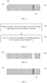
- FIG. 5 is a schematic flowchart of an embodiment of a method for manufacturing an appearance mechanical part according to the present invention.
- Step 501 Arrange a substrate, where the substrate is formed by jointing a metal component and an insulation component.
- the substrate may be formed by compositing the metal component and the insulation component.
- the substrate may be a mobile phone back cover, a mobile phone frame, or the like formed by compositing metal and plastic.
- the metal component and the insulation component may be jointed by means of bonding, clamping, an NMT, and the like.
- a manner of jointing the metal component and the insulation component varies with different quantities and materials of metal components and insulation components. For a specific jointing manner, also refer to the foregoing embodiment. Details are not described herein again.
- two metal components separated from each other may be first arranged, and then a plastic material for connecting the two metal components is injected between the two metal components by using a nano molding technology, to form the substrate.
- the substrate includes two metal components and one insulation component is used.
- two metal components 601 separated from each other may be first arranged.
- a spacing between the two metal components determines a thickness of an insulation component between the two metal components.
- an insulation material is filled between the metal components to form an insulation layer 602 and implement jointing of the insulation component 602 and the metal components 601.
- the plastic material may be injected, by using the NMT technology, between the two metal components separated from each other, so that the plastic material injected between the two metal components forms the insulation component that is jointed with the two metal components, so as to form the substrate.
- Step 502. Form, on a surface of the substrate, an insulation appearance layer covering a jointed boundary line.
- one or more side faces of the surface of the substrate may be selected according to a requirement, and the insulation appearance layer is formed on the one or more side faces.
- the insulation appearance layer covers the jointed boundary interface. There is a jointed boundary line on at least one of the one or more selected side faces, and there is at least one jointed boundary line.
- the insulation appearance layer may be formed in different manners.
- the insulation material may be directly deposited on the selected side face by means of deposition, such as physical vapor deposition (Physical Vapor Deposition, PVD for short) or chemical vapor deposition (Chemical Vapor Deposition, CVD for short).
- PVD Physical Vapor Deposition
- CVD chemical vapor deposition
- the selected side face may be first sandblasted, and then as shown in FIG. 8 , an insulation material is deposited on the surface by means of PVD, so as to form the insulation appearance layer 603.
- a to-be-oxidized metal layer 604 may be deposited on the side face; and then, as shown in FIG. 10 , the to-be-oxidized metal layer is completely oxidized to form the insulation appearance layer 603.
- the to-be-oxidized metal layer may be formed by means of PVD or CVD, and the insulation appearance layer may be formed by performing anodic oxidation on the to-be-oxidized metal layer.
- the to-be-oxidized metal layer and the metal component are made of a same material. As shown in FIG. 10 , to ensure that the to-be-oxidized metal layer is completely oxidized, the metal component may further be partially oxidized in addition to the to-be-oxidized metal layer.
- the metal component of the appearance mechanical part is generally made of aluminum alloy
- the insulation component is generally made of engineering plastic.
- the surface of the substrate may be first sandblasted. By means of sandblasting, impurities on the surface are removed, and the surface is roughened, so that the insulation appearance layer is bonded to the surface more closely.
- a shape of the substrate is a shape of the mobile phone back cover or the mobile phone frame of a mobile terminal.
- a thickness of the to-be-oxidized metal layer may be set according to a requirement, but is required to be less than a maximum thickness of the to-be-oxidized metal layer that may be oxidized by means of anodic oxidation.
Landscapes
- Engineering & Computer Science (AREA)
- Computer Hardware Design (AREA)
- General Engineering & Computer Science (AREA)
- Theoretical Computer Science (AREA)
- Chemical & Material Sciences (AREA)
- Human Computer Interaction (AREA)
- Physics & Mathematics (AREA)
- General Physics & Mathematics (AREA)
- Microelectronics & Electronic Packaging (AREA)
- Chemical Kinetics & Catalysis (AREA)
- Signal Processing (AREA)
- Electrochemistry (AREA)
- Materials Engineering (AREA)
- Metallurgy (AREA)
- Organic Chemistry (AREA)
- Manufacturing & Machinery (AREA)
- Mechanical Engineering (AREA)
- Laminated Bodies (AREA)
- Casings For Electric Apparatus (AREA)
- Telephone Set Structure (AREA)
Applications Claiming Priority (1)
| Application Number | Priority Date | Filing Date | Title |
|---|---|---|---|
| PCT/CN2015/092842 WO2017070822A1 (fr) | 2015-10-26 | 2015-10-26 | Élément structurel apparent et procédé de fabrication d'élément structurel apparent |
Publications (2)
| Publication Number | Publication Date |
|---|---|
| EP3354452A1 true EP3354452A1 (fr) | 2018-08-01 |
| EP3354452A4 EP3354452A4 (fr) | 2018-11-21 |
Family
ID=58629745
Family Applications (1)
| Application Number | Title | Priority Date | Filing Date |
|---|---|---|---|
| EP15906888.1A Withdrawn EP3354452A4 (fr) | 2015-10-26 | 2015-10-26 | Élément structurel apparent et procédé de fabrication d'élément structurel apparent |
Country Status (5)
| Country | Link |
|---|---|
| US (1) | US20180319060A1 (fr) |
| EP (1) | EP3354452A4 (fr) |
| JP (1) | JP2019500249A (fr) |
| CN (1) | CN107107529A (fr) |
| WO (1) | WO2017070822A1 (fr) |
Family Cites Families (6)
| Publication number | Priority date | Publication date | Assignee | Title |
|---|---|---|---|---|
| CN101573009A (zh) * | 2008-04-28 | 2009-11-04 | 富准精密工业(深圳)有限公司 | 电子装置壳体及其制造方法 |
| CN101730410A (zh) * | 2008-10-20 | 2010-06-09 | 深圳富泰宏精密工业有限公司 | 外壳及其制造方法 |
| US8185166B2 (en) * | 2008-10-24 | 2012-05-22 | Apple Inc. | Thermal spray coating for seamless and radio-transparent electronic device housing |
| TW201023716A (en) * | 2008-12-12 | 2010-06-16 | Fih Hong Kong Ltd | Housing for electronic device and method for making the same |
| CN103379753A (zh) * | 2012-04-19 | 2013-10-30 | 深圳富泰宏精密工业有限公司 | 电子装置壳体及其制造方法 |
| US9413861B2 (en) * | 2012-10-05 | 2016-08-09 | Nokia Technologies Oy | Metallization and anodization of plastic and conductive parts of the body of an apparatus |
-
2015
- 2015-10-26 CN CN201580071398.0A patent/CN107107529A/zh active Pending
- 2015-10-26 JP JP2018540191A patent/JP2019500249A/ja not_active Withdrawn
- 2015-10-26 EP EP15906888.1A patent/EP3354452A4/fr not_active Withdrawn
- 2015-10-26 US US15/771,008 patent/US20180319060A1/en not_active Abandoned
- 2015-10-26 WO PCT/CN2015/092842 patent/WO2017070822A1/fr not_active Ceased
Also Published As
| Publication number | Publication date |
|---|---|
| US20180319060A1 (en) | 2018-11-08 |
| EP3354452A4 (fr) | 2018-11-21 |
| JP2019500249A (ja) | 2019-01-10 |
| CN107107529A (zh) | 2017-08-29 |
| WO2017070822A1 (fr) | 2017-05-04 |
Similar Documents
| Publication | Publication Date | Title |
|---|---|---|
| EP3013021B1 (fr) | Boitier, dispositif electronique utilisant celui-ci et son procede de fabrication | |
| US8292663B2 (en) | Audio plug with cosmetic hard shell | |
| US20130257576A1 (en) | Multilayer coil component | |
| CN106299599B (zh) | 壳体、制备天线的方法以及移动终端 | |
| US20160072199A1 (en) | Terminal, terminal-equipped electrical wire, and method for manufacturing terminal-equipped electrical wire | |
| US20190223311A1 (en) | Metal Enclosure Of Mobile Device, Production Method For Metal Enclosure, and Mobile Device | |
| WO2016193669A8 (fr) | Vitrage feuilleté | |
| CN105829852A (zh) | 压差传感器 | |
| EP3354452A1 (fr) | Élément structurel apparent et procédé de fabrication d'élément structurel apparent | |
| CN105551583B (zh) | 扁立线圈用扁平绝缘电线及其制造方法 | |
| EP4234767A3 (fr) | Ensembles d'électroformage pour machines électriques | |
| JP2012195228A (ja) | 雄型端子 | |
| CA2914724A1 (fr) | Procede et appareil de fabrication de fils conducteurs recouverts d'un isolant | |
| US9490593B2 (en) | Connecting plugs to jacks of electronic devices | |
| CN103907246A (zh) | 电容耦合扁平导体连接器 | |
| EP3214624B1 (fr) | Fil électrique isolé et procédé de fabrication correspondant | |
| CN203673847U (zh) | 一种排线 | |
| CN210073373U (zh) | 一种柔性扁平电线电缆 | |
| KR20160091294A (ko) | 구리 피복 알루미늄 복합 선재 | |
| CN206575704U (zh) | 用于制造具有缝隙天线的壳体的基材组件 | |
| CN101505020A (zh) | 电连接器及其结合方法 | |
| CN101847509A (zh) | 可抑制锡须的电容导针 | |
| JP5708256B2 (ja) | 端子付電線及び端子 | |
| CN207234088U (zh) | 一种电气连接结构及电子产品 | |
| JP7074399B2 (ja) | 端子圧着方法 |
Legal Events
| Date | Code | Title | Description |
|---|---|---|---|
| STAA | Information on the status of an ep patent application or granted ep patent |
Free format text: STATUS: THE INTERNATIONAL PUBLICATION HAS BEEN MADE |
|
| PUAI | Public reference made under article 153(3) epc to a published international application that has entered the european phase |
Free format text: ORIGINAL CODE: 0009012 |
|
| STAA | Information on the status of an ep patent application or granted ep patent |
Free format text: STATUS: REQUEST FOR EXAMINATION WAS MADE |
|
| 17P | Request for examination filed |
Effective date: 20180427 |
|
| AK | Designated contracting states |
Kind code of ref document: A1 Designated state(s): AL AT BE BG CH CY CZ DE DK EE ES FI FR GB GR HR HU IE IS IT LI LT LU LV MC MK MT NL NO PL PT RO RS SE SI SK SM TR |
|
| AX | Request for extension of the european patent |
Extension state: BA ME |
|
| A4 | Supplementary search report drawn up and despatched |
Effective date: 20181018 |
|
| RIC1 | Information provided on ipc code assigned before grant |
Ipc: H04M 1/02 20060101ALI20181012BHEP Ipc: B32B 3/10 20060101AFI20181012BHEP Ipc: H05K 5/00 20060101ALI20181012BHEP Ipc: G06F 1/18 20060101ALI20181012BHEP |
|
| DAV | Request for validation of the european patent (deleted) | ||
| DAX | Request for extension of the european patent (deleted) | ||
| STAA | Information on the status of an ep patent application or granted ep patent |
Free format text: STATUS: THE APPLICATION HAS BEEN WITHDRAWN |
|
| 18W | Application withdrawn |
Effective date: 20190429 |